


 View fulltext

2024
Volume: 45 Issue 12
17 Article(s)
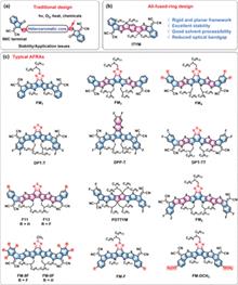
Kai Xiang, Ning Su, Jianhua Chen, and Junqiao Ding
Jan. 15, 2025Vol. 45 Issue 12 120201 (2024)
Shengqiang Zhang, and Zhuoran Wang
Jan. 15, 2025Vol. 45 Issue 12 120401 (2024)
Yujun Xie, Peng Wang, Hongyan Yu, Chengyang Zhong, Jie Peng, Jungan Wang, Chen Yang, Yu Han, Ang Li, Zehao Guan, Feng Qiu, and Ming Li
Jan. 15, 2025Vol. 45 Issue 12 120501 (2024)
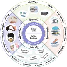
Jinrong Huang, Yuchen Guo, Yongchang Jiang, Feiyu Wang, Lijia Pan, and Yi Shi
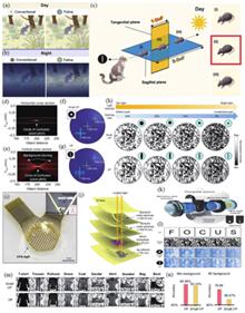
Human skin, through its complex mechanoreceptor system, possesses the exceptional ability to finely perceive and differentiate multimodal mechanical stimuli, forming the biological foundation for dexterous manipulation, environmental exploration, and tactile perception. Tactile sensors that emulate this sensory capability, particularly in the detection, decoupling, and application of normal and shear forces, have made significant strides in recent years. This review comprehensively examines the latest research advancements in tactile sensors for normal and shear force sensing, delving into the design and decoupling methods of multi-unit structures, multilayer encapsulation structures, and bionic structures. It analyzes the advantages and disadvantages of various sensing principles, including piezoresistive, capacitive, and self-powered mechanisms, and evaluates their application potential in health monitoring, robotics, wearable devices, smart prosthetics, and human-machine interaction. By systematically summarizing current research progress and technical challenges, this review aims to provide forward-looking insights into future research directions, driving the development of electronic skin technology to ultimately achieve tactile perception capabilities comparable to human skin.
Jan. 15, 2025Vol. 45 Issue 12 121601 (2024)
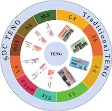
Xin Shi, Weiguo Wang, Jun Wang, Jian Li, and Huamin Chen
Triboelectric nanogenerator (TENG) utilizing tribovoltaic effect can directly produce direct current with high energy conversion efficiency, which expands their application in semiconductor devices and self-powered systems. This work comprehensively summarizes the recent developments in semiconductor-based direct current TENGs (SDC-TENGs), which hold significant promise for DC energy harvesting technologies and semiconductor systems. First, the tribovoltaic effect is elucidated, and SDC-TENGs are categorized into six types based on different triboelectric structures: metal?semiconductor (M?S), metal?insulator?semiconductor (M?I?S), semiconductor?semiconductor (S?S), semiconductor?insulator?semiconductor (S?I?S), liquid?semiconductor (L?S), and metal/semiconductor?liquid?semiconductor (M/S?L?S) contact devices. Subsequent sections detail the operational mechanisms, strengths, and limitations of each category. Additionally, this paper outlines the enhancement mechanisms of SDC-TENGs providing guidance and recommendations for performance improvement. The conclusion highlights potential application scenarios for various types of SDC-TENGs, outlining the prospective benefits and challenges. SDC-TENG technology is poised to drive revolutionary developments in semiconductor devices and self-powered systems.
Jan. 15, 2025Vol. 45 Issue 12 121701 (2024)
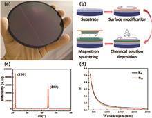
Juwon Lee, Chang-Hyeon Jo, Gwangseop Lee, Min-Sung Bae, Slawomir Prucnal, Shengqiang Zhou, Muhammad Zubair Khan, Osama Gohar, Mohsin Saleem, and Jung-Hyuk Koh
In this study, aluminum-doped zinc oxide (AZO) thin films were deposited onto a low-temperature polyethylene terephthalate (PET) substrate using DC magnetron sputtering. Deposition parameters included power range of 100?300 W, a working pressure of 15 mTorr, and a substrate temperature of 50 °C. Post-deposition, flash lamp annealing (FLA) was employed as a rapid thermal processing method with a pulse duration of 1.7 ms and energy density of 7 J·cm?2, aimed at enhancing the film's quality while preserving the temperature-sensitive PET substrate. FLA offers advantages over conventional annealing, including shorter processing times and improved material properties. The structural, optical, and electrical characteristics of the AZO films were assessed using X-ray diffraction, field emission scanning electron microscopy coupled with energy-dispersive X-ray spectroscopy, ultraviolet?visible spectroscopy, and Hall effect measurements. The results demonstrated that properties of AZO films varied with deposition and annealing conditions. Films deposited at 200 W and subjected to FLA exhibited superior crystallinity, with average visible light transmittance exceeding 80% and resistivity as low as 0.38 Ω·cm representing 95% improvement in transmittance. Electrical analysis revealed that carrier concentration, mobility, and resistivity were influenced by both sputtering and annealing parameters. These findings underscore the effectiveness of FLA in optimizing AZO thin film properties, highlighting potential in optoelectronics applications.
Jan. 15, 2025Vol. 45 Issue 12 122101 (2024)

Yiwen Zhang, Jun Deng, Zonghu Li, Xinyou Liu, Haiou Li, Baochuan Wang, Jun Luo, Zhenzhen Kong, Gang Cao, Guoping Guo, Chao Zhao, and Guilei Wang
Ge/SiGe heterostructure quantum wells play a pivotal role in the pursuit of scalable silicon-based qubits. The varying compressive strains within these quantum wells profoundly influence the physical characteristics of the qubits, yet this factor remains largely unexplored, driving our research endeavor. In this study, we utilized RP-CVD (Reduced Pressure Chemical Vapor Deposition) to grow Ge quantum wells with varied compressive strain, proposing growth schemes for lightly-strained (ε∥ = ?0.43%) QW (quantum well), standard-strained (ε∥ = ?0.61%) QW, and heavily-strained (ε∥ = ?1.19%) QW. Through comprehensive material characterization, particularly employing the low-temperature magneto-transport measurements, we derived the percolation densities ranging from 4.7 × 10¹⁰ to 14.2 × 1010 cm?2 and mobilities from 3.382 × 10⁵ to 7.301 × 105 cm2?V?1?s?1. Combined with the first-principles calculations, our analysis delves into the trends in effective mass and percolation density at low temperatures, shedding light on the impact of quantum effects on band structures and the interplay between structural components and wave functions. This research offers a comprehensive investigation into the intrinsic mechanisms governing complex multi-strained quantum wells, spanning growth, characterization, and computational perspectives, thereby establishing a strategy for the growth of high-quality strained quantum wells.
Jan. 15, 2025Vol. 45 Issue 12 122102 (2024)
Thi Kim Oanh Vu, Thi Thu Phuong Bui, Ngoc Anh Nguyen, Thi Thanh Bao Nguyen, Thi Minh Hien Nguyen, and Eun Kyu Kim
Recently, there has been considerable interest in high-efficiency ultraviolet (UV) photodetectors for their potential practical uses. In this study, a high-quality UV photodetector was fabricated using a combination of Ag and Au NPs with GaN film. The GaN film was deposited using sputtering technique, whereas Ag and Au films were grown using thermal evaporation technique. Ag?Au bimetallic nanoparticles were formed by treating them at the various annealing temperature to improve the interaction between light and the photoactive layers of the photodetectors. The optimal annealing temperature to achieve the best performance of a photodetector is 650 °C. This led to a photoresponsivity of 98.5 A/W and the ON/OFF ratio of 705 at low bias voltage of 1 V. This work establishes the foundation for the advancement of high-performance UV photodetectors.
Jan. 15, 2025Vol. 45 Issue 12 122301 (2024)
Tianyang Feng, Jialin Meng, Hang Xu, Yafen Yang, Tianyu Wang, Hao Zhu, Qingqing Sun, David Wei Zhang, and Lin Chen
Simulating the human olfactory nervous system is one of the key issues in the field of neuromorphic computing. Olfactory neurons interact with gas molecules, transmitting and storing odor information to the olfactory center of the brain. In order to emulate the complex functionalities of olfactory neurons, this study presents a flexible olfactory synapse transistor (OST) based on pentacene/C8-BTBT organic heterojunction. By modulating the interface between the energy bands of the organic semiconductor layers, this device demonstrates high sensitivity (ppb level) and memory function for NH3 sensing. Typical synaptic behaviors triggered by NH3 pulses have been successfully demonstrated, such as inhibitory postsynaptic currents (IPSC), paired-pulse depression (PPD), long-term potentiation/depression (LTP/LTD), and transition from short-term depression (STD) to long-term depression (LTD). Furthermore, this device maintains stable olfactory synaptic functions even under different bending conditions, which can present new insights and possibilities for flexible synaptic systems and bio-inspired electronic products.
Jan. 15, 2025Vol. 45 Issue 12 122302 (2024)
Yafen Yang, Hang Xu, Tianyang Feng, Jianbin Guo, and David Wei Zhang
The advanced fin-shaped field-effect transistor (FinFET) technology offers higher integration density and stronger channel control capabilities, however, more complex process effects are also introduced which have significant influence on device performance. To address these issues, we complete a design-technology co-optimization (DTCO) focused on FinFET, including both process-induced effect during gate formation and corresponding digital unit optimization design. The 14 nm FinFET complementary metal oxide semiconductor (CMOS) technology is used to illustrate the sensitivity of transistor performance to process-induced effect, specifically the poly pitch effect (PPE) and cut poly effect (CPE). Predictive technology computer aided design (TCAD) simulations have been carried out to evaluate the transistor performance in advance. Based on the results, optimizations in digital unit design is proposed. Fall delay of the digital unit inverter is decreased by 0.7%, and the rise delay is decreased by 2.1%. For multiple selector (MUX2NV), the delay decreases by 4.64% for rise and 3.56% for drop, respectively.
Jan. 15, 2025Vol. 45 Issue 12 122303 (2024)
Daryoosh Vashaee
This study presents a comprehensive optimization and comparative analysis of thermoelectric (TE) infrared (IR) detectors using Bi2Te3 and Si materials. Through theoretical modeling and numerical simulations, we explored the impact of TE material properties, device structure, and operating conditions on responsivity, detectivity, noise equivalent temperature difference (NETD), and noise equivalent power (NEP). Our study offers an optimally designed IR detector with responsivity and detectivity approaching 2 × 10⁵ V/W and 6 × 109 cm?Hz1/2/W, respectively. This enhancement is attributed to unique design features, including raised thermal collectors and long suspended thin thermoelectric wire sensing elements embedded in low thermal conductivity organic materials like parylene. Moreover, we demonstrate the compatibility of Bi2Te3-based detector fabrication processes with existing MEMS foundry processes, facilitating scalability and manufacturability. Importantly, for TE IR detectors, zT/κ emerges as a critical parameter contrary to conventional TE material selection based solely on zT (where zT is the thermoelectric figure of merit and κ is the thermal conductivity).
Jan. 15, 2025Vol. 45 Issue 12 122304 (2024)
Lulu Zheng, Xianglong Bi, Xuhong Ma, Guibin Liu, Binbin Liu, Kang Zhou, and Hua Li
Frequency combs with equally spaced frequency lines show great potentials for applications in spectroscopy, imaging, communications, and so on. In the terahertz frequency region, the quantum cascade laser (QCL) is an ideal radiation source for frequency comb and dual-comb operation. The systematic evaluation of phase noise characteristics of terahertz QCL frequency comb and dual-comb sources is of great importance for high precision measurements. In this work, we present detailed measurements and analysis of the phase noise characteristics of terahertz QCL frequency comb and dual-comb sources emitting around 4.2 THz with repetition frequencies of ~6.2 GHz. The measurement results for the current noise of the direct current (DC) sources (that are used to electrically pump the terahertz QCLs) indicate that at 100 Hz, the current noise for DC-1 and DC-2 is 0.3895 and 0.0982 nA/Hz1/2, respectively. Such levels of current noise can be safely disregarded. The phase noise of radio frequency (RF) generators (that are employed for injection locking and phase locking), intermode beatnotes, and dual-comb signals with and without phase-locked loop (PLL) are all measured and compared. The experimental results show that in the free-running mode, the phase noise of the intermode beatnote signals is always lower than that of the dual-comb signals across all frequencies. Additionally, the phase noise induced by the RF generators is negligible. By employing the phase locking technique, the phase noise of the intermode beatnote and dual-comb signals in the low offset frequency band can be significantly suppressed. At an offset frequency of 100 Hz, the measured phase noise values of the dual-comb line without and with phase locking are 15.026 and ?64.801 dBc/Hz, respectively.
Jan. 15, 2025Vol. 45 Issue 12 122401 (2024)
Yifan Yao, Suhao Yao, Jiaqing Yuan, Zeng Liu, Maolin Zhang, Lili Yang, and Weihua Tang
In this work, a PEDOT:PSS/Sn:α-Ga2O3 hybrid heterojunction diode (HJD) photodetector was fabricated by spin-coating highly conductive PEDOT:PSS aqueous solution on the mist chemical vapor deposition (Mist-CVD) grown Sn:α-Ga2O3 film. This approach provides a facile and low-cost p-PEDOT:PSS/n-Sn:α-Ga2O3 spin-coating method that facilitates self-powering performance through p?n junction formation. A typical type-Ⅰ heterojunction is formed at the interface of Sn:α-Ga2O3 film and PEDOT:PSS, and contributes to a significant photovoltaic effect with an open-circuit voltage (Voc) of 0.4 V under the 254 nm ultraviolet (UV) light. When operating in self-powered mode, the HJD exhibits excellent photo-response performance including an outstanding photo-current of 10.9 nA, a rapid rise/decay time of 0.38/0.28 s, and a large on/off ratio of 91.2. Additionally, the HJD also possesses excellent photo-detection performance with a high responsivity of 5.61 mA/W and a good detectivity of 1.15 × 10¹¹ Jones at 0 V bias under 254 nm UV light illumination. Overall, this work may explore the potential range of self-powered and high-performance UV photodetectors.
Jan. 15, 2025Vol. 45 Issue 12 122402 (2024)
Bo Chen, Baojie Zhu, Yifan Wu, Pengpeng Sang, Jixuan Wu, Xuepeng Zhan, and Jiezhi Chen
Graphene oxide, as a 2D material with nanometer thickness, offers ultra-high mobility, chaotic properties, and low cost. These make graphene oxide memristors beneficial for reservoir computing (RC) networks. In this study, continuous-wave (CW) laser processing is used to reduce chaotic graphene oxide (CGO) films, resulting in the non-volatile storage capability based on the reduced chaotic graphene oxide (rCGO) films. Laser power significantly impacts the characteristics of the rCGO memristor. Material characterization indicates that laser radiation can effectively reduce the oxygen content in CGO films. With optimized laser power, the rCGO memristor achieves a large ratio at 18 mW laser power. Benefiting from the short-term memory characteristics, distinct conductive states are achieved, which are further utilized to construct RC networks. With a third control probe, the rCGO memristor can express rich reservoir states, demonstrating accuracy in predicting the Hénon map with an NRMSE below 0.3. These findings provide the potential for developing flexible RC networks based on graphene oxide memristors via laser processing.
Jan. 15, 2025Vol. 45 Issue 12 122403 (2024)
Yi Huang, Qiurui Chen, Rongyao Ma, Kaifeng Tang, Qi Wang, Hongsheng Zhang, Ji Ding, Dandan Xu, Sheng Gao, and Genquan Han
This paper presents a comprehensive analysis of the short-circuit failure mechanisms in commercial 1.2 kV planar silicon carbide (SiC) metal–oxide–semiconductor field-effect transistors (MOSFETs) under 400 and 800 V bus voltage conditions. The study compares two products with varying short-circuit tolerances, scrutinizing their external characteristics and intrinsic factors that influence their short-circuit endurance. Experimental and numerical analyses reveal that at 400 V, the differential thermal expansion between the source metal and the dielectric leads to cracking, which in turn facilitates the infiltration of liquid metal and results in a gate–source short circuit. At 800 V, the failure mechanism is markedly different, attributed to the thermal carrier effect leading to the degradation of the gate oxide, which impedes the device's capacity to switch off, thereby triggering thermal runaway. The paper proposes strategies to augment the short-circuit robustness of SiC MOSFETs at both voltage levels, with the objective of fortifying the device's resistance to such failures.
Jan. 15, 2025Vol. 45 Issue 12 122501 (2024)
Junfei Wang, Junhui Hu, Chaowen Guan, Songke Fang, Zhichong Wang, Guobin Wang, Ke Xu, Tengbo Lv, Xiaoli Wang, Jianyang Shi, Ziwei Li, Junwen Zhang, Nan Chi, and Chao Shen
Low-resistance Ohmic contact is critical for the high efficiency GaN-based laser diodes. This study investigates the introduction of the In0.15Ga0.85N contact layer on the specific contact resistance. Experimental results reveal that adopting the In0.15Ga0.85N contact layer yields a minimized specific contact resistance of 2.57 × 10?5 Ω·cm2 which is two orders of magnitude lower than the GaN contact layer (7.61 × 10?3 Ω·cm2). A decrease in the specific contact resistance arises from the reduction of the barrier between the metal and p-type In0.15Ga0.85N. To develop an optimal metal electrode combination on the In0.15Ga0.85N contact layer, the Pd/Au and Ni/Au electrode stacks which are most commonly used in the formation of Ohmic contact with p-GaN are investigated. Metal stack of 10/30 nm Pd/Au is demonstrated effective in reducing the specific contact resistance to 10?5 Ω·cm2 level. The mechanism of the variation of the specific contact resistance under different annealing atmospheres is explained by auger electron spectroscopy.
Jan. 15, 2025Vol. 45 Issue 12 122502 (2024)
Kaiyue He, Zhanqi Li, Taotao Li, Yifu Sun, Shitong Zhu, Chao Wu, Huiping Zhu, Peng Lu, Xinran Wang, and Maguang Zhu
Owing to the unique characteristics of ultra-thin body and nanoscale sensitivity volume, MoS2-based field-effect transistors (FETs) are regarded as optimal components for radiation-hardened integrated circuits (ICs), which is exponentially growing demanded especially in the fields of space exploration and the nuclear industry. Many researches on MoS2-based radiation tolerance electronics focused on the total ionizing dose (TID) effect, while few works concerned the displacement damage (DD) effects, which is more challenging to measure and more crucial for practical applications. We first conducted measurements to assess the DD effects of MoS2 FETs, and then presented the stopping and ranges of ions in matter (SRIM) simulation to analysis the DD degradation mechanism in MoS2 electronics. The monolayer MoS2-based FETs exhibit DD radiation tolerance up to 1.56 × 10¹³ MeV/g, which is at least two order of magnitude than that in conventional radiation hardened ICs. The exceptional DD radiation tolerance will significantly enhance the deployment of MoS2 integrated circuits in environments characterized by high-energy solar and cosmic radiation exposure.
Jan. 15, 2025Vol. 45 Issue 12 122701 (2024)
© Copyright 2018-2021 | Chinese Laser Press.
All Rights Reserved 沪ICP备15018463号-20