


 View fulltext

2024
Volume: 53 Issue 11
24 Article(s)

Shunli HE, Xianling MENG, Ning CAO, Bin XIA, Chuanlong SUN, Ruhan LUAN, and Lichun ZHANG
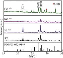
In recent years, fully inorganic copper-based chalcogenide materials have gradually become a research hotspot in the field of novel optoelectronic devices due to their high stability, lead-free and low toxicity, and excellent optoelectronic properties. Compared with traditional lead-containing based chalcogenides, fully inorganic copper-based chalcogenides have significant advantages in terms of environmental friendliness and long-term stability, and thus are widely recognised as potential candidates for next-generation high-performance optoelectronic materials. Among many copper-based chalcogenides, Cs?Cu?Br?, as a typical fully inorganic copper-based chalcogenide, has received extensive attention from domestic and foreign research teams for its excellent environmental stability and good optoelectronic performance. According to the current reports, it is known that most of the preparation methods of Cs?Cu?Br? materials use the solution method. However, the films prepared by the solution method often have a large number of holes, which seriously affects the photoelectric properties of the films. These holes not only reduce the optical uniformity and crystalline quality of the films, but also may introduce surface defects, which in turn lead to a significant degradation of the device performance. Therefore, choosing an appropriate film growth method becomes one of the keys to enhance the performance of Cs?Cu?Br? films. For this reason, finding methods that can effectively reduce holes and improve the densification of thin films has become the focus of research. The aim of this work is to obtain high quality Cs?Cu?Br? films by optimizing the film growth process. In the study, Cs?Cu?Br? thin films were prepared on silicon substrates by vacuum thermal evaporation, and the effects of the growth temperature on the film morphology, crystalline quality and optical properties were systematically investigated. Vacuum thermal evaporation, as a physical vapor deposition method, can effectively improve the crystallinity and surface flatness of the films by controlling the deposition rate and substrate temperature. In this study, it was found that the growth temperature had a significant effect on the quality of Cs?Cu?Br? films. Under the optimal conditions, the prepared Cs?Cu?Br? thin films exhibited excellent morphological characteristics, with a flat and dense film surface, very few holes, and good crystallinity. In addition, the films exhibit strong absorption in the deep ultraviolet region (270 nm) and are capable of emitting bright blue light (460 nm), which indicates that the films have excellent optical properties. The optical band gap of the films is 4.31 eV, which meets the requirements for deep-UV photovoltaic applications. Based on the optimally grown high-quality Cs?Cu?Br? films, Cs?Cu?Br?/n-Si heterojunction photodetectors were further prepared in this study. The heterojunction photodetector exhibits a remarkable photoresponse in the deep-ultraviolet band (270 nm), with a response rate of 0.47 mA/W, corresponding to a detection rate of 2.09×10? Jones.This result indicates that the photoelectricity performance of Cu-based chalcogenides can be significantly enhanced by optimizing the growth process of the films, thus providing new possibilities for their application in deep-ultraviolet photodetection. It is shown that Cs?Cu?Br? thin films not only excel in stability and lead-free environmental friendliness, but also exhibit high potential for application in deep-ultraviolet photodetectors. In this study, a new method for the preparation of high-performance Cs?Cu?Br? thin films based on vacuum thermal evaporation technology is proposed, and the morphology and optoelectronic properties of the films are significantly improved by systematically regulating the growth temperature. This not only provides an effective way for the preparation of silicon-based Cs?Cu?Br? thin films, but also lays the foundation for the development of high-performance Cu-based deep-ultraviolet photodetectors. This research result is of great significance for the wide application of lead-free and environmentally friendly chalcogenide materials in optoelectronic devices in the future.
Nov. 25, 2024Vol. 53 Issue 11 1104001 (2024)
Qin XIAO, Zhengzhou LI, and Haiyi LIU
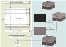
Infrared imaging non-uniformity severely degrades the quality of infrared images, reducing their clarity and sensitivity, and thereby limiting the effective application of various subsequent infrared image algorithms. To eliminate infrared imaging non-uniformity and improve the quality of infrared images, this paper proposes a novel infrared imaging non-uniformity correction method based on scene-adaptive directional guided filtering, extending the traditional neural network non-uniformity correction algorithm. First, this paper analyzes the causes of non-uniformity in infrared images and proposes a model for infrared non-uniformity generation. It is concluded that infrared non-uniformity manifests as vertical stripe patterns in the vertical direction. Based on this characteristic, the paper improves the Canny extraction algorithm with dual-threshold characteristics and uses the improved Canny algorithm to extract detailed features of infrared images. The dual-threshold characteristic can suppress infrared non-uniformity while extracting detailed image features. This extracted feature is then used to adaptively adjust the regularization factor of the traditional guided filter, resulting in the proposed scene-adaptive directional guided filter. Traditional guided filters process the entire image using uniform linear models and regularization factors, which cannot adequately preserve detailed image information. Although guided filters can protect image edges and textures while smoothing the image, there are still deficiencies when estimating the desired image for the neural network correction algorithm: 1) Guided filters use the same regularization factor for all local windows in the image, without considering the differences in detailed textures within different windows. Therefore, the original guided filter does not sufficiently protect the detailed features of the image. 2) The uncorrected infrared image contains stripe non-uniformity and pixel response non-uniformity. Although the intensity of these non-uniformities is weaker than that of the scene edge features, their presence causes a large local window variance even in flat areas of the image. The guided filter cannot adapt to the characteristics of infrared non-uniformity, leading to a lack of smoothing in local areas that should be smoothed, thus retaining the non-uniformity. The regularization factor is an inherent parameter of the guided filter, used to enhance the stability of the guided filter. The original guided filter applies the same regularization factor to all areas, failing to reflect the differences in detailed features across different regions. Therefore, it is necessary to adjust the penalty factor based on image details, i.e., to adaptively adjust the regularization factor by calculating the penalty factor using local edge detail features of the image. The proposed scene-adaptive directional guided filter adaptively calculates the Canny edge feature response of non-uniform images within local windows and uses this response feature to compute a penalty factor to adjust the guided filter's regularization factor. This method estimates a more realistic scene image, preserving image details and improving the robustness of the correction algorithm. The scene-adaptive directional guided filter enables the neural network correction process to obtain infrared expected images closer to the real scene, significantly enhancing the overall performance of the neural network non-uniformity correction algorithm. Additionally, to address the issue of ghosting commonly associated with neural network correction algorithms, this paper employs a motion detection mechanism and adaptive adjustment of the neural network learning rate to suppress ghosting artifacts. Extensive experiments on infrared non-uniformity image correction validate that the proposed method effectively preserves detailed image information while suppressing infrared pixel non-uniformity and stripe non-uniformity. This enhances the effectiveness and robustness of the non-uniformity correction algorithm. In conclusion, the proposed scene-adaptive directional guided filter-based infrared imaging non-uniformity correction method effectively corrects infrared non-uniformity, preserves detailed image information, and improves the robustness and effectiveness of neural network-based non-uniformity correction algorithms. This advancement facilitates the application of subsequent infrared target detection algorithms, significantly enhancing the quality and reliability of infrared imaging.
Nov. 25, 2024Vol. 53 Issue 11 1110001 (2024)
Yi CAO, Xiangping ZHU, Xiaomo ZHANG, Wei ZHAO, and Jun MA
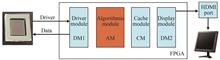
The development of Electron-Bombarded Complementary Metal-Oxide-Semiconductor (EBCMOS) technology marks a significant advancement in image sensors, particularly enhancing low-light and night vision applications. This paper addresses challenges in device development due to material and manufacturing imperfections that introduce complex noise into night vision imagery. Additionally, it highlights the drawbacks of traditional software-based image processing platforms, including their low real-time performance and high operational costs.An analysis of low-light imaging characteristics of EBCMOS, developed by the Xi'an Institute of Optics and Mechanics, is presented. This research introduces a multi-stage pulse noise suppression and edge enhancement algorithm, designed on a Xilinx-FPGA platform, tailored to tackle mixed noises such as Poisson noise, salt-and-pepper noise, and speckle noise prevalent in low-light conditions.EBCMOS sensors are distinctive in their ability to enhance visibility in dark environments through an electron-bombarding mechanism that amplifies signals before CMOS processing. This capability is crucial for applications requiring high-quality night vision, such as security surveillance and wildlife monitoring. The imperfections in materials and fabrication processes can result in various noise types, degrading image quality and obscuring critical details.The paper details a sophisticated FPGA-based algorithm that leverages modern processing power to efficiently reduce noise while preserving important image details. This is achieved through advanced noise reduction techniques that specifically target the unique characteristics of each noise type, improving upon traditional methods like median filtering and Gaussian blurring. Experimental results show that this algorithm enhances the Peak Signal-to-Noise Ratio (PSNR) by 11.37% over median filtering and 26.64% over Gaussian blurring.Moreover, the processing speed for a single image frame is improved approximately 21 times compared to software platforms on high-end processors, demonstrating the algorithm's capability to handle real-time image processing tasks efficiently. This not only suggests potential cost reductions but also supports the integration and miniaturization of wearable night vision devices.In summary, this study provides significant insights into the benefits of FPGA-based image processing for EBCMOS technology in night vision applications. The advancements facilitate more effective and efficient night vision systems and promote the development of integrated, lightweight wearable devices, offering substantial benefits for both military and civilian uses.
Nov. 25, 2024Vol. 53 Issue 11 1110002 (2024)
Weiwei LI, Tongyi ZHANG, Yan KANG, Ruikai XUE, Xiaofang WANG, Jintao LIANG, and Lifei LI
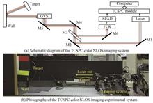
Non-Line-Of-Sight (NLOS) imaging is a special optical imaging technique. It refers to the technique of reconstructing an image of an object in the event of an occlusion between the imaging system and an object that cannot be directly observed. It is to collect and analyze the photon signal returned from the target through the intermediate surface (such as wall, floor, etc.), to realize the image reconstruction of the target scene. NLOS imaging can be divided into active and passive depending on whether an active illumination source is used or not. Passive NLOS imaging systems rely primarily on the object itself emitting light or reflecting ambient light for imaging. Active NLOS imaging systems generally use a laser source for active illumination, it can obtain 3D image of the NLOS target through collecting time-resolution photon data. With the development of semiconductor single-photon detectors, Single-Photon Avalanche Photodiode (SPAD) detectors have gradually been widely used in active NLOS imaging technology due to their advantages of single photon detection sensitivity and picosecond temporal resolution, small size and low power consumption. However, in previous studies, researchers always used single-wavelength laser source to illuminate, and the reconstructed images of the targets only provide grayscale information of the target. In this paper, we demonstrate a color NLOS imaging method based on Time-Correlated Single-Photon Counting (TCSPC) and multi-wavelength laser illumination. First, we built a NLOS imaging system using confocal optical path mode, adopt a SPAD detector and a picosecond multi-wavelength pulsed laser. Then, the phasor field virtual wave algorithm is used to reconstruct the data collected by the three wavelength channels of 620 nm±1.5 nm, 532 nm±1.5 nm and 485 nm±1.5 nm, respectively. Finally, the three images obtained through different wavelength channels are synthesized to obtain a color NLOS image. In the experiments, targets containing different color information were selected for color NLOS imaging verification. The emitting laser repetition rate was set to 9.73 MHz, and the average power of the three wavelength lasers of 620 nm, 532 nm, and 485 nm were 255.9 μW, 100.8 μW, and 179.7 μW, respectively. A Silicon SPAD with a time jitter of 40 ps was used for echo photon detection. A 45 cm×45 cm wooden board with white wallpaper on its surface was used as the intermediate wall. The intermediate wall was 1 m away from the NLOS imaging system, and the target was 0.2 m away from the intermediate wall. The laser beam was controlled to scan 20×20 pixels on the intermediate wall and the interval between scanning points is 2 cm. The single point scanning time is 20 s. Under the above experimental parameter settings, NLOS imaging was performed on two targets containing four colors of red, white, yellow, and orange. By analyzing the PSNR of the imaging results, it can be obtained that the PSNRs of the 620 nm channel, the 532 nm channel, the 485 nm channel, and the synthetic color NLOS image are 7.9 dB, 7.4 dB, 6.7 dB, and 9.2 dB, respectively. This proves that the complementary detection of the three wavelengths can be used to obtain color NLOS imaging results with enhanced image quality. In summary, our proposed color NLOS imaging method can reconstruct the color image of complex NLOS targets with white, red, yellow and orange color features. Meanwhile, the complementarity of multi-wavelength detection can restore the 3D NLOS image with more complete details, which further expands the information dimension of NLOS imaging technology. In the future, it is planned to design a beam splitting system for the back-end receiving optical path and increase the number of SPAD detectors to detect more wavelengths simultaneously, so as to achieve high-efficiency TCSPC color non-line-of-sight imaging.
Nov. 25, 2024Vol. 53 Issue 11 1111001 (2024)
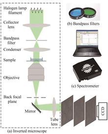
Ying LI, Man NUO, Yutong ZHANG, Shijia HUA, Yanan CAI, Hui CHEN, Dong DUAN, Chunxi HAO, and Wenyi REN
Most samples of interest in the fields of optical measurements, adaptive optics, materials physics and biomedical imaging are phase object. Such samples change very little in the amplitude part of the transmitted light, but the different refractive index or thickness distribution of the samples results in a very large change in the phase part of the transmitted light. The human eye or detector can only record the change in intensity caused by the object but cannot determine its phase change. Due to its non-invasive nature, label-free capability, and ability to provide quantitative measurements, quantitative phase imaging technology has emerged as a preferred tool for obtaining phase information in these areas. Techniques in quantitative phase imaging, particularly those based on the Transport of Intensity Equation (TIE), offer advantages such as non-interferometric operation, non-iterative processing, and compatibility with modern bright-field microscopes, has already found application in various domains. However, TIE was derived under the assumption of fully coherent light. In the field of optical microimaging, the use of partially coherent light illumination generated by modern optical microscopes is important for improving imaging quality and suppressing coherent noise. Given that the illumination source in the microscope Kohler illumination system is usually in the form of a combination of halogen lamps and band-pass filters, the resulting illumination light is polychromatic with a certain bandwidth. Under the conditions of lower spatial and temporal coherence of illumination, TIE is still applicable if the sample to be measured does not have a strong dispersion of the illumination wavelength. However, since the definition of mean phase is inherently tied to the choice of mean wavelength, a challenge in the phase reconstruction emerges due to the complexity in fixing a specific mean wavelength. The mean illumination wavelength is often approximated by the center wavelength of the bandpass filter. This approximation overlooks the polychromatic light transmission characteristics of different bandpass filters. If the spectral distribution curve of the light after the halogen lamp passes through the bandpass filter has central symmetry, the peak spectral wavelength can be determined as the central wavelength. However, if the spectral distribution curve does not have central symmetry, directly determining the peak spectral wavelength as the mean wavelength may increase the reconstruction error of the mean phase. To address the above problems, this paper proposes an optimal mean wavelength method, we carried out numerical simulation and experiments using broadband polychromatic radiation with known spectral distributions. The polychromatic intensity is obtained by integrating the monochromatic intensity across wavelengths through numerical simulation, and then the axial differentiation of the intensity is calculated. The mean phase of the polychromatic beam is determined based on the fast Fourier transform based TIE solution algorithm, and the reconstructed mean phases at different mean wavelengths are quantitatively analyzed to determine the optimal mean wavelength for different bandpass filters. By adding Gaussian noise to the polychromatic intensity to simulate actual measurement noise and quantization effects, we further investigate the influence of different defocus distances on the selection of optimal mean wavelength and the recovered phase accuracy. Experimental results on microlens arrays with known height information show that when the spectral distribution curve has good central symmetry, using the spectral peak wavelength as the center wavelength performs comparable to the optimal mean wavelength method. When the spectral distribution curve does not have good central symmetry, the optimal mean wavelength method can reduce the reconstruction error of the sagittal height of the microlens array compared with the peak center wavelength method at the same defocus distance.
Nov. 25, 2024Vol. 53 Issue 11 1111002 (2024)
Zhao CHEN, Wenpeng LIU, Yu SUN, Jinhong JIANG, Jinyun GAO, Xiaofei WANG, Guihua SUN, Renqin DOU, Deming ZHANG, Jianqiao LUO, and Qingli ZHANG
In recent years, high power solid-state lasers have been developing in the direction of higher average power and larger pulse energy, which puts higher and higher requirements on the size and quality of the laser crystal materials. The preparation of high quality laser crystals with larger size has become one of the important issues to be solved in laser development, so the thermal bonding technology has become an effective technical way to prepare large size laser crystals. Thermal bonding technique, also known as diffusion bonding technique, is a process in which two precise-machined crystal interfaces are pressed together and combined through van der Waals force or hydrogen bond, and then heated to form an integrated uniform crystal by ion thermal diffusion. The preparation of composite crystals by the thermal bonding technology has been widely used in laser field. The composite crystals can not only significantly improve the thermal management of high power lasers and obtain high optical quality lasers, but also is an important way to prepare larger crystals. However, in the process of the bonded crystals preparation, due to the factors such as uneven pressure and uneven distribution of temperature field during heating, the bonding surface will produce bubbles, holes, cracks and other defects, which seriously affect the quality and success rate of the bonded crystals. The Hot Isostatic Pressing (HIP) technique is to place the components to be treated in a closed container, and apply the same pressure to the components and apply high temperature at the same time. Under the action of high temperature and high pressure, the internal defects of the components can be eliminated. By combining HIP technology with the thermal bonding technology and controlling hot isostatic pressing parameters, the internal defects of bonded crystals after sintering can be reduced or eliminated.In this paper, the treatment of large size Yb∶YAG/Yb∶YAG composite laser crystals by hot isostatic pressing technique was studied. The hot isostatic pressing of Yb∶YAG/Yb∶YAG composite laser crystals was carried out under different temperature, time and pressure. The quality of the components after hot isostatic pressing was characterized by bending strength, elastic modulus, Vickers hardness, transmission spectrum and optical uniformity. By means of metallographic microscope, pore elimination and defect closure in bonded crystals were observed, and the mechanism of defect reduction or elimination by HIP was studied by analyzing the change of intergranular stress. The experimental results show that hot isostatic pressing is beneficial to improve the properties of large size and high quality composite crystals at 1 600 ℃ and 200 MPa. After HIP treatment, the bubbles and defects on the bonding surface of the bonded crystal elements are greatly reduced, the bending strength is increased by 185.29%, the Vickers hardness is increased by 16.14%, and the optical transmittance and optical uniformity are significantly improved. After hot isostatic pressing, all the bubbles and defects on the bonding surface of the composite laser crystal are eliminated, and the mechanical and optical properties of the composite laser crystal are obviously improved, and the properties are basically consistent with those of Yb∶YAG single crystal. With the continuous deepening and improvement of the research, it can provide a basis for the performance optimization and wide application of bonded crystals.
Nov. 25, 2024Vol. 53 Issue 11 1114001 (2024)

Yanqing JIA, Hailing WANG, Ranzhe MENG, Jianxin ZHANG, and Xuyan ZHOU
In modern optical communication, Dense Wavelength Division Multiplexing (DWDM) technology provides the possibility of simultaneous transmission of multiple signals and improvement of information transmission capacity, and the multi-wavelength monolithic integrated silicon-based laser arrays with small wavelength intervals in a dense DWDM silicon-based optical system has become a research hotspot and a difficult point. However, traditional multi-wavelength monolithic integrated silicon-based laser array with 0.8 nm wavelength spacing based on first-order uniform gratings are difficult to achieve due to the limitation of sub nanometer processing accuracy. In this paper, a four-channel monolithic integrated Ⅲ-V/Si laser array with 0.8 nm wavelength spacing based on silicon waveguide distributed Bragg sampling gratings is demonstrated. Firstly, it is proposed to design and manufacture a set of distributed Bragg sampling gratings at both ends of the silicon waveguides in four channels, as front and rear mirrors, to form the resonant cavity of each channel Ⅲ-V/Si laser. Secondly, by changing the micro-meter level sampling period of the silicon waveguide distributed Bragg sampling grating of four channels, four different wavelengths corresponding to the +1st sub-gratings of the four channel silicon waveguide distributed Bragg sampling gratings are selected to oscillate in the resonant cavity and emit. In the proposed laser, the silicon waveguide's width, height, and ridge etch depth are fixed as 1.5 μm, 0.34 μm, and 0.22 μm, respectively. The Ⅲ-V layer stack has eight strained InAlGaAs Quantum Wells (QWs) with graded index separate confinement hetero-structure layers. The front and rear mirrors'length are set 100 μm and 400 μm, respectively. In the simulation design, the etching depth of the seed grating of the Bragg sampling grating of the silicon waveguide distribution of each channel is set to 30 nm, the duty cycle is 50%, the period of the seed grating Λ0 is 266 nm, and the other parameters are the same as those in 1.1 of this paper, and the corresponding excitation wavelength of the seed grating is 1 635 nm. Then the overall effective refractive index neff of the silicon waveguide distribution Bragg sampling grating of one of the channels is calculated, and the sampling period P of the silicon waveguide sampling grating of this channel is set to 6.3 μm, the excitation wavelength corresponding to the positive first-order seed grating of the silicon waveguide sampling grating of this channel is calculated to be 1 570 nm. According to the above method, keeping other parameters unchanged and only changing the sampling period P of the other three channels of silicon waveguide sampling gratings, three different wavelengths corresponding to the positive primary sub-gratings of the three channels of silicon waveguide sampling gratings are calculated. Finally, four different excitation wavelengths of 1 569.2 nm, 1 570 nm, 1 570.8 nm, 1 571.6 nm are obtained for the four-channel Ⅲ-V/Si laser array based on the silicon waveguide distributed Bragg sampling grating. The four +1st wavelengths are within the gain spectrum of Ⅲ-V epitaxial material, while the corresponding 0st wavelength of the seed grating is outside the gain spectrum of Ⅲ-V epitaxial wafer, which satisfies the excitation conditions of the corresponding wavelengths of the positive 1st order sub-gratings of the sampling grating of the four-channel Ⅲ-V/Si laser array. Meanwhile, in order to improve the coupling efficiency between the Ⅲ-V active waveguide and the silicon waveguide, a two-stage Ⅲ-V tapered waveguide is designed at both ends of the Ⅲ-V active waveguide for each channel of the Ⅲ-V/Si laser. The first segment is the Ⅲ-V tapered waveguide 1, and the second segment is the Ⅲ-V tapered waveguide 2. The width of the Ⅲ-V tapered waveguide 1 decreases from 4 μm to 1 μm, and the width of the Ⅲ-V tapered waveguide 2 decreases from 1μm to 0.8 μm. Simulation demonstrates that when the length of the Ⅲ-V tapered waveguide 2 is larger than 40 μm, the evanescently coupling efficiency between the Ⅲ-V active waveguide and the silicon waveguide reaches more than 99%, and the light can be efficiently coupled from the Ⅲ-V active waveguide into the silicon waveguide. To fabricate such a device, ?rstly the distributed Bragg sampling and silicon waveguide are fabricated on the 100-oriented silicon-on-insulator wafer by photolithography, e-beam lithography and dry etching. Then, the Ⅲ-V epitaxial wafer is transferred onto SOI wafer with a low temperature directly wafer bonding technology. Ⅲ-V epitaxial wafer and SOI wafer need acetone isopropanol cleaning and HF aqueous solution surface treatment before directly wafer bonding. After physical connecting of Ⅲ-V epitaxial wafer and SOI wafer, the wafers are put into a wafer bonding machine with a 1.5 MPa pressure and low vacuum, under the 150 ℃ bonding temperature for hours. By solving the directly wafer bondingtechnology, the patterned silicon on insulator wafers and Ⅲ-V epitaxial wafers is heterogeneous integrated together, achieving self-alignment of four-channel Ⅲ-V waveguides and four-channel silicon waveguides without the sub-micrometer level passive or active alignment technology. Finally, after three-step Ⅲ-V etching, 4 μm width and 1.7 μm depth current channel is formed to prevent lateral diffusion of carriers, MQW taper is to couple light to the silicon waveguide effectively, N-InP etch is to remove N-InP on the grating, respectively. Ti/Au metal stack is deposited as contact metals for p-type and n-type electrodes. The fabrication of micrometer level sampling period avoids the sub-nanometer processing required for fabricating first-order uniform gratings. Ultimately, a four-channel Ⅲ-V/Si laser array is fabricated. Under continuous wave conditions at room temperature, the output power of the single-wavelength from each channel silicon waveguide is greater than 0.7 mW@60 mA, the threshold current is less than 25 mA, and the lasing wavelengths are 1 569.64 nm, 1 570.45 nm, 1 571.27 nm, and 1 572.08 nm, respectively, with a wavelength spacing of 0.8 nm ± 0.2 nm. This type of the Ⅲ-V/Si laser array is easy to integrate on a large area with high density, and can further achieve more channels of Ⅲ-V/Si laser arrays with wavelength spacing of 0.8 nm or even smaller. After further optimization, this type of Ⅲ-V/Si laser array can be applied in dense wavelength division multiplexing silicon optical systems.
Nov. 25, 2024Vol. 53 Issue 11 1114002 (2024)
Ruixin NIU, Wenyu GAO, Qiang ZHANG, Yanan ZHANG, Yuan ZHOU, Manman LI, Xiaohao XU, Shaohui YAN, and Baoli YAO
The Imaginary Poynting Momentum (IPM) is associated to the imaginary part of the well-known complex Poynting vector. When light fields interact with matter, researchers usually pay attention to the real part of the complex Poynting vector, while neglect its imaginary part. However, the real Poynting vector describes only a portion of the physical mechanism underlying light-particle interaction. Recent theoretical and experimental breakthrough have been made in the study of the IPM force, which has gained increasing interest that the IPM force is independent of the optical radiation pressure and intensity gradient force. It provides a new degree of freedom for optical micromanipulation with structured light, such as vector beams, evanescent and two-wave interference fields. The IPM force can be detected directly with a Mie particle in the tightly focused Spirally Polarized Vector Beam(SPVB) when the IPM appears in the azimuthal direction. Nevertheless, the spinning optical torque caused by the vortex-like structure of IPM has not been investigated. In order to study the rotational manipulation of particles by this IPM vortex, we use the Finite-Difference Time-Domain (FDTD) method, to investigate the spinning optical torque acting on microparticles, illuminated by the SPVB, and to study the influence of the particle material properties on the torque. The cylindrical vector beam is constructed by the in-phase superposition of the radially and azimuthally polarized vector beam. When the angle of polarization is π/4, this cylindrical vector beam is the spirally polarized vector beam characterized by the IPM arising in the azimuthal direction. The FDTD method is a prevailing solution that can be used to solve Maxwell's equations and optomechanics for arbitrarily shaped particles. The scattering problem of arbitrary particles can be handled, so the FDTD method is characterized by high inclusivity and high accuracy. The spinning torque is computed rigorously based on the Maxwell stress tensor method, or the conservation of optical angular momentum of the total field. By changing the wavelength of the incident field as well as the size, shape and material of the particles, the spinning optical torque characteristics of the particles under the SPVB are analyzed comprehensively. The computation results show that this SPVB can induce the spinning optical torque, which drives the microparticle to spin about their own axis. For rod-like particles, the spinning optical torque increases first, and then decreases with the increase of incident wavelength. There is the phenomenon of resonance peaks explained by the multipole resonances induced in the particles. The spinning optical torque tends to increase first and then decrease with the increase of particle's length, and the spinning optical torque reaches the maximum value at particle's length around 2 μm. Moreover, it is found that, for the particles with complex geometrical structures (e.g., equilateral-triangle, hexagonal and chiral structures), the spinning optical torque is at least one order of magnitude larger than that of the rod-shape particle, and the values and directions of the spinning optical torques are more varied. On complex geometrically structured particles of certain sizes and materials, due to the effect of resonance, there are overall large value and opposite direction for the spinning optical torques. The particles selected in this paper have some special shapes, but for generic isotropic particles, IPM can also induce them to spin. This reveals a new method for achieving light-driven microrotors, which does not rely on the optical angular momentum. The azimuthal IPM complements the spin and orbital angular momenta in terms of their rotational mechanical effects, which has potential applications in the field of optical micromanipulation and levitated optomechanics, especially in the realization of unusual optomechanical manifestations such as the negative or left-handed optical torque.
Nov. 25, 2024Vol. 53 Issue 11 1126001 (2024)
Xueli DONG, Guoxia HAN, Yihan TIAN, Ke HU, Xianghua YU, and Kaiyun ZHAN
Photonic nanojet is a kind of highly focused subwavelength locally electromagnetic beam that is formed by the scattering of dielectric micro-particle on light field, when the symmetry of system that is composed of light field and micro-particle is broken, a kind of subwavelength locally curved beam is formed, photonic hook. It is featured by a sub-diffraction limit of half-height width and a much smaller radius of curvature than wavelength. Due to these excellent performance parameters, the photonic hook has broad application prospects in the field of optical imaging, optical manipulation and trapping. Since the concept of photonic hook was proposed, researchers have been exploring the factors influencing the effective length and bending angle of photonic hooks, such as the parameters related to the properties of the medium particles (e.g., size, structure, material) and the characteristics of the light field. Among them, most studies focus on the exploration of the structure of the micro-particle, and many different structures have been developed, but the material of the micro-particle is a dielectric or an artificial material. The state of water cylinder is changed at freezing, so frozen water cylinder can be a phase change material. Using frozen water droplet as phase change materials and the ice-water interface as plane, the generation of time-domain self-bending photonic hook has attracted much attention. However, the generated photonic hook has a relatively small effective length and a small curvature. During the freezing process of water cylinder, the shape at the state transition does not have a quantitative model for description. This paper sets the functions as boundaries for the state transition of materials and introduces the idea of functions from mathematics into the device design of photonic hooks. A twin photonic hook generator is designed using frozen water cylinder as phase change materials and function surfaces as the ice-water boundary interface. The software COMSOL is used for simulation, and effective control of the characteristic parameters of the photonic hooks was achieved by altering the structure of the frozen water cylinder and the coefficients of the functions. The variation patterns of characteristic parameters such as effective length, bending angle, and the bending number of the photonic hooks were analyzed. The results show that the coefficients A, B, and C are respectively related to the opening angle, rotation direction, and depth of concavity of the function. The opening of the ice-water boundary obtains a twin photonic hook when there is symmetry with respect to the direction of illumination. As the asymmetry increases, the twin photonic hook gradually transforms into a single photonic hook. When the ice-water boundary opening increases under symmetric incidence, the effective length shows an initial growth followed by a decrease trend. Meanwhile, the bending angle also shows an initial increase followed by a decrease trend. Moreover, during the gradual enlargement of the opening, the phenomenon of multiple bending of the photonic hook becomes more pronounced. When the concave depth continues to increase, the effective length initially decreases and then shows a lengthening trend, while the overall bending angle shows an initial increase followed by a decrease trend. Among them, the maximum bending angle of the photonic hook can reach up to 44° (A=14.79, B=0, C=-9, D=0), the maximum effective length can reach up to 17.43λ (A=177.51, B=0, C=-12, D=0), and the number of bending cycles can reach up to 4. Compared to traditional methods, this design introduces functions to achieve research on more complex structures of photonic hooks and further enables the modulation of characteristic parameters of photonic hooks. This provides new insights for the design and research of photonic hooks, while also offering references for their applications in areas such as optical manipulation and biomedicine.
Nov. 25, 2024Vol. 53 Issue 11 1126002 (2024)
Fu WAN, Zhiyi LUO, Hongcheng SUN, Rui WANG, Yaotian BAI, Yingkai LONG, and Weigen CHEN
High-precision monitoring of multi-component gases is crucial in diverse fields such as environmental monitoring, agricultural development, industrial safety, and medical diagnosis. Laser Raman spectroscopy provides a unique capability to simultaneously detect multiple gases by exploiting the distinct Raman frequency shift characteristics of each gas. However, the sensitivity of gas detection remains suboptimal due to the limited Raman scattering cross-section and weak scattering effect, posing a barrier to widespread adoption. To overcome these limitations, this study utilizes cavity enhancement technology to augment the detection sensitivity of Raman spectroscopy.However, the resonance of the Fabry-Perot (F-P) cavity is vulnerable to external environmental factors such as vibration and temperature drift. Therefore, frequency locking technology is necessary to maintain cavity resonance stability in practical applications, ensuring the generation of stable intra-cavity high power. Optical feedback frequency locking technology achieves this by locking the semiconductor laser into a high-precision external cavity using a slow servo system, eliminating the need for strict linewidth matching conditions. Nonetheless, in complex environments, perturbations from machinery or airflow can induce phase changes that exceed the adjustment range of the servo loop. This rapidly diminishes the capability to identify phase deviations, resulting in poor performance of the PID controller and unstable Cavity Transmission Signals (CTS).To tackle these challenges, this paper proposes a novel feedback phase adjustment approach. Firstly, utilizing the established laser cavity coupling model, a comprehensive analysis of the optical feedback phase's impact on cavity transmission signal is conducted. Theoretical findings suggest that compensating for deficiencies in the shape of the cavity transmission signal as a phase deviation indicator can be achieved by considering the signal strength. Subsequently, the entire 2π period is divided into four distinct regions based on CTS asymmetry and maximum value. Each region employs different error signals for phase adjustment. When the feedback phase significantly deviates while being close to the peak, a proportional coefficient, contingent upon the degree of asymmetry, is multiplied to serve as the feedback phase error control, thus readjusting the phase to the optimal position. The phase deviation tolerance of the phase-locked system spans the entire 2π interval, simplifying the process of obtaining the initial phase either manually or through algorithmic means.An optical feedback Raman spectroscopy gas detection platform was designed and constructed. Experimental validation demonstrates that the proposed optical feedback phase-locked method exhibits superior stability and robust recovery capability in scenarios involving strong and rapid airflow disturbances. This significantly enhances the potential of optical feedback cavity-enhanced Raman spectroscopy gas detection technology for real-time, in-situ detection scenarios. The detection limits for O2 and N2 in air were measured at 4.8 Pa (48.83 μL/L) and 5.8 Pa (57.43 μL/L), respectively. The minimum detection limit for a 10% CO2 standard gas concentration is 4.4 μL/L under the conditions of a gas chamber pressure of 3 atm and an integration time of 200 s.
Nov. 25, 2024Vol. 53 Issue 11 1130001 (2024)
Fu WAN, Yaotian BAI, Rui WANG, Lei ZHU, Yingkai LONG, and Weigen CHEN
The oil-immersed power transformer represents a pivotal component within the framework of a power system. The accurate detection of power transformer operation status and the issuing of fault warnings are of great significance in ensuring the safe and reliable operation of the power grid. The composition and content of dissolved gases in transformer oil are closely related to the fault state of the transformer. One of the most effective methods for diagnosing the operational state of a transformer is the accurate detection and analysis of the characteristic gases associated with transformer faults. Trace gas sensing based on laser spectroscopy plays a pivotal role in numerous fields, including environmental monitoring, urban surveillance, industrial process control, medical diagnostics, and agronomy. Raman spectroscopy is based on the Raman scattering effect of matter, which can be used to detect all gases except single atom gases. The simultaneous qualitative and quantitative analysis of multi-component gases can be achieved by utilizing a single wavelength laser. Nevertheless, the extremely low Raman scattering cross-section of gas represents a significant limitation in the detection sensitivity of Raman spectroscopy, which in turn constrains its broad applicability in the field of trace gas detection and analysis. Fiber-Enhanced Raman Spectroscopy (FERS) is a Raman scattering signal enhancement technology based on hollow fibers. Its objective is to improve the collection efficiency of Raman scattered light. However, the balance time required for gas to enter the fiber is too long. Cavity-Enhanced Raman Spectroscopy (CERS) employs the linear correlation between the Raman signal and laser power to enhance the Raman signal of gases and improve the sensitivity of gas detection by stabilizing the laser to a linear Fabry-Pérot (F-P) cavity, thereby enabling the accumulation of optical power. One of the key issues associated with F-P cavity enhancement technology based on optical feedback frequency locking is the potential for the direct reflection light of the resonator input mirror to interfere with the laser frequency locking, thereby preventing the accumulation of power within the cavity. Consequently, it is imperative to attenuate the intensity of the direct reflection light during the optical feedback frequency locking process. At present, the optical feedback frequency locking technology must forego the simplicity and sensitivity of the Cavity-Enhanced Raman Spectroscopy (CERS) gas sensing system in order to circumvent the direct reflection of the resonant cavity, which would otherwise compromise the frequency locking and power accumulation. This paper proposes a simple and highly sensitive optical feedback frequency locking asymmetric cavity mirror linear F-P cavity enhanced Raman spectroscopy gas detection technology. The phase relationship between resonant light and direct reflection light is analyzed. The influence of attenuated direct reflection on optical feedback frequency locking is analyzed using the cavity reflected light field function. The theoretical analysis of the influence of direct reflection and the resonant light feedback coefficient on the intensity of the reflected light field is presented. A novel asymmetric mirror linear F-P cavity direct reflection attenuation model is proposed. The results of the simulation demonstrate that the optical feedback frequency locking range gradually increases with a reduction in the reflectivity of the cavity input mirror. The theoretical feasibility of achieving optical feedback frequency locking in a linear F-P cavity by reducing the reflectivity of the front mirror in order to attenuate direct reflection is demonstrated. On this basis, an optical feedback frequency locking asymmetric cavity mirror linear F-P cavity enhanced Raman spectroscopy detection platform was designed and constructed. In order to verify the feasibility of the asymmetric cavity mirror linear F-P cavity direct reflection attenuation model, frequency locking experiments were performed using cavity input mirrors with different reflectivity. By regulating the reflectivity of the cavity input mirror to be significantly lower than that of the cavity output mirror, the resonant light is dominant in the reflected light, and the optical feedback frequency locking is successfully achieved. Finally, a plane mirror with a reflectivity of 99.96% and a flat concave mirror with a reflectivity of 99.994% were selected as the front and rear mirrors of the linear F-P cavity, respectively. The laser was able to establish a stable basic transverse mode TEM00 power accumulation within the cavity. When the input power is 80 mW, the laser power in the cavity is approximately 320 W, and the gain multiple is 4 000 times. The backward Raman scattering light collection method was employed. In the context of a gas chamber pressure of 0.1 MPa and an integration time of 60 s, the detection limits of the optical feedback frequency-locked asymmetric cavity mirror linear F-P cavity enhanced Raman spectroscopy detection platform for the main fault characteristic gases CH4, C2H6, C2H4, C2H2, CO and CO2 of the transformer were 1.3, 4.4, 2.7, 1.2, 10.5 and 5.1 μL/L, respectively. The optical feedback frequency locking asymmetric cavity mirror linear F-P cavity enhanced gas Raman sensing system exhibits high detection sensitivity and high spectral resolution, rendering it a promising candidate for transformer fault characteristic gas detection. A more sensitive detection limit can be achieved by utilizing a higher power diode laser, a higher reflectivity cavity mirror and an increased integration time. The asymmetric cavity mirrors direct reflection attenuation model proposed in this paper can also be employed to lock the frequency of other types of diode lasers to a linear F-P cavity. The technology of cavity-enhanced spectroscopy has the potential to be of significant value in a number of applications.
Nov. 25, 2024Vol. 53 Issue 11 1130002 (2024)
Yanheng WANG, Yun LI, Can YU, Xiangyu GAO, and Shuang WANG
In order to adequately correct the response nonlinearity of infrared detectors, the multi-point method is often used to replace the traditional two-point method for the radiometric correction of satellite-borne infrared spectral imagers, and the number of required calibration temperature points increases with the increase of the dynamic range. Aiming at the redundancy of temperature points in multi-point calibration, a calibration temperature point selection method based on relative standard deviation threshold division is proposed. Firstly, the experimentally obtained instrumental response curve is divided into multiple segments using the standard deviation method, and each segment is linearly fitted using the least-squares method to ensure the fitting accuracy; secondly, the calibration coefficients derived from the fitting are inversely performed to determine the blackbody temperature points for two-point calibration in each segment. The same method is used to divide the nonlinear response curves within all spectral segments, and the corresponding calibrated temperature points for all sub-segments of each segment after division are found. Finally, all the temperature points are combined and compressed to determine the final calibration temperature points. In order to verify the feasibility of the method, simulation experiments and real experiments were carried out respectively. The nonlinear response of a single spectral band was simulated, and the standard deviation method and the bisection method were used to divide multiple bands under the same division conditions (relative standard deviation of 1%), and the least-squares method was used for linear fitting after division, resulting in the need for 14 calibrated temperature points after the division of the standard deviation method and the need for 22 calibrated temperature points after the bisection method, and the degree of nonlinearity of the two methods after the division of the fit was less than 1%. It can be proved that the standard deviation method can reduce the number of calibration temperature points under the same division requirements. When the number of calibration points is the same (20), the standard deviation method and the uniform division of the two methods are used to fit the nonlinear response curve of a single spectral band. The maximum value of nonlinearity was 0.404 6% after fitting by standard deviation method and 1.059 9% after uniform division and linear fitting. It can be proved that when the number of calibration temperature points is the same, the standard deviation method is better than the uniform division. Combined with the designed infrared spectral imager, 17 spectral channel response curves at mid-wave were simulated, and the nonlinear response curves of each spectral channel were divided into multiple segments using the standard deviation method, and the 17 spectral segments were divided into 72 segments under the condition of 1% relative standard deviation. The blackbody temperature points used for two-point calibration were derived for each sub-segment. Since the temperature points derived from the inversion of each segment are not necessarily unique, and the same blackbody temperature point can be adapted to radiometric calibration in different bands. Therefore, the temperature points can be combined according to their frequency of occurrence. The combined calibrated temperature points (90) are compressed. Using the compressed 10 calibrated temperature points to calibrate 17 spectral bands, the nonlinearity of the calibrated multiband linear response curve is less than 1%. Infrared radiation acquisition experiments were conducted, and the nonlinear response curve of the mid-wave infrared camera in the temperature range of 308.15~396.15 K in the blackbody grew linearly to saturation was measured. Using the standard deviation method for multi-segment division, 14 calibration points are required after division, and the maximum value of the nonlinearity after linear fitting is 0.61%, and the mean value is 0.48%. The results of both simulation and measurement experiments show that this method can be effectively used for the selection of temperature points for the multi-segment two-point calibration method, which is of certain significance for reducing the burden of the infrared spectral imager in orbit, lowering the number of temperature points for blackbody calibration, and realizing efficient on-planet blackbody nonlinear calibration.
Nov. 25, 2024Vol. 53 Issue 11 1130003 (2024)
Jinlong ZHANG, Shuangying LI, Qize WU, Hongfei JIAO, Xinbin CHEN, and Zhanshan WANG
There has been significant progress in the research and development of Far Ultraviolet (FUV) thin film devices, driven by growing demands in astrophysics, geophysics, and other fields. However, most materials exhibit strong absorption in the FUV region, posing challenges for optical element design due to the limited material options. To address this issue, extensive research has been conducted on materials, structures, and fabrication processes.Aluminum (Al) mirrors are the primary components in FUV devices, and fluorides are commonly employed as protective layers to prevent Al from oxidizing. Al+LiF and Al+MgF? mirrors have already been used in space telescopes like Far Ultraviolet Spectroscopic Explorer (FUSE) and Hubble Space Telescope (HST). The influence of deposition rate, substrate temperature, and protective layer thickness on the performance of these mirrors has been investigated. High-performance Al+eLiF (enhanced LiF) and Al+eMgF? (enhanced MgF?) mirrors were prepared by QUJIADA M A et al. using a three-step deposition method, which is currently considered a reliable approach to enhance the reflectivity of Al mirrors effectively. The absorption edge of LiF is about 105 nm, making it the transparent material with the shortest absorption edge known in nature, and a commonly used material for FUV short-wavelength band protective layers. However, LiF is hygroscopic, leading to poor time stability in Al+LiF mirrors. ANGEL D W et al. suggested that MgF? could effectively slow down the aging of Al+LiF, which led to the development and validation of protected Al+LiF mirrors. Al+LiF+MgF? and Al+LiF+AlF? mirrors have significantly improved time stability compared to Al+LiF films.Fluoride materials known for their low absorption and high stability, such as MgF?, AlF?, and LaF?, have become prevalent in FUV reflective filters. By utilizing a multi-periodic dielectric structure with alternating high and low refractive index materials, (LaF?/MgF?)? reflective filters have been successfully fabricated, centered at wavelengths of 135.6 nm and 121.6 nm. Higher reflectivity and narrower bandwidths were achieved by optimizing the design and fabrication processes. The successful fabrication of narrowband mirrors, such as Al+LiF+SiC+LiF and Al+LiF+B?C, has achieved the goal of suppressing the H Lyman α line in the solar spectrum. Furthermore, based on the (Al/MgF?)? structure, a transmission filter with a central wavelength of 121.6 nm has been realized. Optimization of the design and fabrication processes holds the promise of achieving higher transmittance and narrower bandwidths.The optical constants of thin films are fundamental for characterizing their performance, but they vary significantly under different conditions, especially in the FUV region. Optical constants for materials in the FUV range are relatively scarce. Conventional measurement methods, such as photometry, least squares fitting, and Kramers-Kronig analysis, have yielded optical constants for certain materials, such as MgF?, LaF?, and others.Despite these advancements, significant limitations still exist in FUV materials, and research on thin-film devices remains insufficient. More systematic and in-depth investigations into precise thin-film fabrication and environmental stability are needed. The field of FUV thin films holds vast potential for future development. Future research will focus on exploring new materials, optimizing structures, and innovating fabrication processes to broaden their applications.New materials with features such as higher optical performance, greater environmental stability, and broader operating wavelengths are sought to overcome the limitations of current materials. Further optimization of deposition methods, such as incorporating Atomic Layer Deposition (ALD) technology and other advanced fabrication techniques, is to develop efficient and precise manufacturing processes, obtaining more accurate optical constants through extensive measurements and establishing a comprehensive database of FUV optical constants. The design of more rational multilayer structures utilizing the properties of different materials, coupled with precise characterization and control, achieves wider bandwidths and higher reflectivity mirrors. Conducting in-depth studies on the impact of various environmental conditions on performance and developing effective protective measures, thereby enhance both performance and stability.A more comprehensive regulating of thin-film optical properties can be achieved by continuously exploring new materials, optimizing structural designs, and innovating fabrication processes. This will provide more precise data and theoretical guidance for optical element design, enabling the fabrication of more efficient FUV optical elements and driving advancements in optical device technology. Driven by increasing demands for astronomical observation, FUV thin-film devices are poised for significant performance improvements. It is anticipated that FUV reflective thin films will find broader applications in fields such as space exploration, lithography, and medical diagnostics.
Nov. 25, 2024Vol. 53 Issue 11 1131001 (2024)
Ming TANG, Shuang LU, Zhanglin HU, Shuhui LI, Chao YUN, Yinzhuo HU, Jie CHEN, Wenbin LI, and Zhanshan WANG
Since the appearance of Extreme Ultraviolet (EUV) and X-Ray Free-Electron Lasers (XFEL), there has been a significant interest in studying radiation damage on thin-film optical components. The mechanisms of laser-induced damage on thin films are closely related to various factors such as wavelength, pulse duration, material type, film thickness, and notably, the initial temperature of film. In this study, a combined approach using the two-temperature model and molecular dynamics was employed to investigate the influence of initial temperature on the melting damage mechanism of nickel films irradiated by EUV free-electron laser with a wavelength of 13.5 nm. The melting damage thresholds of Ni films at various initial temperatures have been determined, revealing a decrease in thresholds with increasing initial temperature and the presence of two distinct linear intervals. Specifically, within the temperature range of 300 to 900 K, the linear regression slope is -0.125 J/cm2/K, whereas the slope shifts to -0.200 J/cm2/K between 900 K and 1 300 K. Two distinct melting behaviors were observed by analyzing the atomic snapshots of irradiated films: the homogeneous melting inside the films with the initial temperature of 300~900 K, and the heterogeneous melting on the surface of films with the initial temperature of 900~1 300 K. It may be the reason for these two linear intervals existing in the relationship between the melting damage absorption fluence and the initial temperature. By analyzing the temperature and the stress variations over time and space, it was found that the different damage behaviors are mainly related to the lattice overheating, the thermoelastic stress induced by FEL and the lattice average heating rate. For Ni films with initial temperatures below 900 K, the melting damage under FEL irradiation induces significant tensile stress within the films, which leads to the reduction of equilibrium melting temperature and causes localized overheating. Furthermore, the lattice stability is compromised under high stress and the increased lattice average heating rate enhances the probability of internal liquid phase nucleation. Conversely, for Ni films with initial temperatures above 900 K, the internal stress remains relatively low when the melting damage occurs, which results in a lower probability of liquid phase nucleation within the films. Nevertheless, on the film surface, the formation of liquid phase nuclei is more likely due to a lower surface free energy.
Nov. 25, 2024Vol. 53 Issue 11 1131002 (2024)
A Reconfigurable Microwave Photonic Filter Based on an Optical Recirculating Frequency Shifting Loop
Quan CHEN, Guangying WANG, Zhenzhao YI, Yuan CAO, Xinhuan FENG, and Baiou GUAN
Microwave Photonic Filters (MPFs) can find applications in the fields of optical communications, radar, optical fiber sensing. Due to the implementing of high-frequency optical signals and different optical processing devices, MPFs can achieve low loss, large bandwidth and compatible communication. To construct a finite impulse response MPF, researchers have proposed a variety of tapping and delay structures. An MPF can be classified as coherent one or incoherent one, according to the coherent characteristic of the adopted optical carriers. A simple approach of Phase-Modulation to Intensity-Modulation(PM-IM) conversion is usually used to construct a coherent MPF, but the frequency response of the MPF is limited by the adopted optical filter. The principle of the incoherent MPFs is based on the impulse response filters, which are constructed through multiple taps and time delays. One of the important indicators to evaluate the performance of the MPFs is the reconfigurability. In terms of tap implementation, using physical paths with equally spaced time delay is a common method, but this requires complicated switching structures to tune the length of each optical path. Another common approach is to use multi-wavelength sliced broadband optical sources or incoherent laser arrays, combined with dispersion fibers to achieve time delay. Usually, the positive coefficient MPFs require incoherent light sources to reduce interference between the adjacent taps, but it will increase the system noise. Therefore, how to achieve a high signal-to-noise ratio incoherent filter with tunable and reconfigurable performance is one of the critical issues that needs to be solved urgently in the field of microwave photonic signal processing.In this paper, an MPF with a simple structure and a high reconfigurability is demonstrated based on an optical Recirculating Frequency Shifting Loop (RFSL). By adding a Single-Sideband(SSB)modulator to an optical fiber loop, a new optical frequency component will be generated each time when the optical carrier passes through the SSB modulator which is modulated by a microwave signal. As a result, the proposed RFSL not only has an equally spaced comb-like spectrum in the frequency domain but also an equally spaced time delay between the adjacent optical carriers in the time domain. It can be found that a traditional MPF based on an RFSL mainly utilized its multi-carrier characteristics in the frequency domain and the time delay between the taps is achieved by using dispersive optical fibers. However, the time domain characteristics of the RFSL have not yet been effectively developed. In fact, the equally spaced time delay characteristic of the RFSL can be also used to introduce a time delay between different taps. Since the frequency difference between the multiple optical carriers generated by the RFSL is larger than the bandwidth of the photodetector, the intensity interference caused by the high coherence of the optical carriers can be avoided, and a stable spectral response can be achieved. By using a Programmable Optical Filter(POF) to shape the spectrum generated by the RFSL, different tap numbers can be controlled, and the weight of each tap can be precisely adjusted, thereby obtaining an effective tuning of the Free Spectral Range(FSR), tap number and weight.In the experiment, the output optical signal from the RFSL is delivered to the POF which is a Waveshaper, for spectral shaping. The POF provides a series of discrete frequency channels for the filtering of each carrier and modulation sideband of RFSL. After the k-th optical carrier is attenuated to a certain extent, any adjustable tap weight can be obtained. In terms of tunable reconfigurability, we propose to use the POF to change the delay between taps, and allocate new channels to each comb group (both carrier and sidebands) in the original RFSL. We experimentally demonstrated the switching of the tap number between 2, 5, and 10 with an FSR of 3.85 MHz, and the switching of the FSR between 3.85 MHz, 1.925 MHz, and 770 kHz with a tap number of 2. Through spectral shaping, we have achieved an MPF with a reconfiguration of the tap number and the FSR. Moreover, when the tap number is 5 or 10, the MPF with reconfigurable tap number has a Main to Secondary Sidelobe Ratio(MSSR)of 11 dB. On the other hand, the optical amplifier in the RFSL is an Erbium-Doped Fiber Amplifier(EDFA)which can bring a high small signal gain, the long erbium-doped fiber length will also increases the cavity length of the RFSL, which decreases the FSR in the experiment. The cavity length can be further reduced through using a Semiconductor Optical Amplifier(SOA), and other devices such as Polarization Controllers(PCs), Tunable Optical Filters(TOFs), pigtails and jumpers such as Dual-Parallel Mach-Zehnder Modulator(DPMZM)can all be optimized to reduce the optical length. Different from non-frequency-shifting loops, RFSL does not require much incoherence of the optical carrier source. Even under a small loop length, a stable multi-tap signal can still be obtained. Through further optimization, the FSR of the MPF we proposed can be increased to 100 MHz.
Nov. 25, 2024Vol. 53 Issue 11 1106001 (2024)
Jia LIU, Yukang LIAO, Jiacheng TU, Jiashun LI, and Hao LIU
Pressure detection under high temperature environments has an urgent need in aerospace, equipment development, petrochemical and other fields. Especially, with the development of space industry and the research of new generation engines, in-situ pressure measurement of key parts such as pipes, chambers and combustion chambers plays an important role in engine test, combustion instability analysis, mode switching of engine systems and so on. Consequently, it is highly necessary to research on the design, manufacture and testing methods of the sensors. Compared with the traditional electrical sensors, fiber-optic sensor has the advantages of small size, long transmission distance and immunity to electromagnetic interference. Through the analysis of the high temperature pressure sensors based on fiber-optics Fabry-Perot principle, the operating temperature is mainly limited by the sensor composition material, sensitive unit processing method, signal transmission mode and demodulation method. The high-temperature resistance performance of sensitive materials directly determines the upper temperature limit of the sensor. Thermal stress mismatch is another significant factor causing the failure of sensors in harsh environments. In addition, the transmission and extraction methods of the characteristic signal are the difficult points of high-temperature pressure sensors. To address the above limitations, there are many researches on quartz, silicon, silicon carbide, sapphire and other high-temperature resistant materials as sensitive unit in high temperature region to improve the operating temperature. Meanwhile, MEMS and femtosecond laser processing methods have great advantages in sensor consistency and thermal stress matching manufacturing. Among the single-crystal oxide materials, single crystal magnesium oxide material shows high application value in the fields of high-temperature fiber-optic sensing because of its ultra-high melting point, excellent optical and mechanical properties. In this paper, combining the advantages of magnesium oxide material and MEMS processing technology, a magnesium oxide wafer optical fiber Fabry-Perot pressure sensor based on MEMS for harsh monitoring is proposed. The square Fabry-Perot cavity is designed to improve the pressure sensitivity. The thermal stress matching machining of the sensitive element is realized by developing the wet etching and direct bonding technology of magnesium oxide. Meanwhile, the optical fiber is integrated for pressure detection in high-temperature environments. The structural parameters of the sensor are optimized by the mechanical, thermal and modal simulation results. The pressure experiments at room temperature and high temperatures are carried out to verify the large pressure range and temperature response performance of the sensor. The experimental test results demonstrate that the FP cavity length of the sensor during the increasing and decreasing pressure over three cycles varies linearly with the pressure in the range of 15 MPa at room temperature with a nonlinear error of 0.75%FS. Additionally, error bars diagram is drawn to analyze the uncertainty and reliability of the sensor test results, which indicates that the sensor test results are relatively reliable. The high temperature pressure test results show that the sensor can be effectively measured in the range of 22 ℃ to 800 ℃. For each temperature, the FP cavity length decreases with the pressure, and the cavity length approximately linearly changes with the pressure over the entire test range, even up to 800 ℃. Therefore, the experiment results demonstrate that the sensor can stably operate at an environment of 22~800 ℃ and 0~0.7 MPa. This work is of fundamental importance in realization of pressure detecting in ultra-high environments. And the application of magnesium oxide in the field of optical sensing provides a new way to solve in-situ pressure measurement at high temperatures, narrow spaces or other related positions of aeroengines.
Nov. 25, 2024Vol. 53 Issue 11 1106002 (2024)
Qiang CHEN, Junzhe LIANG, and Jin LIANG
Traditional Digital Image Correlation (DIC) methods face challenges in terms of computational speed, especially for large datasets, and in handling complex scenarios involving high-frequency deformation or discontinuities such as cracks. With the advent of deep learning, the potential for leveraging Convolutional Neural Networks (CNNs) for DIC has become increasingly apparent. Deep learning has revolutionized computer vision, achieving state-of-the-art results in tasks such as image classification, object detection, and segmentation. The success of CNNs in these domains suggests that they could also be applied to the task of DIC, potentially offering improvements in both accuracy and computational efficiency.In this context, the publication presents a novel approach to DIC using an advanced CNN architecture known as UNet++. The proposed method, termed DIC-Net++, is designed to address the limitations of traditional DIC algorithms and enhance the performance of deep learning in the context of speckle image deformation measurement. The article has developed two specialized networks within the DIC-Net++ framework: DIC-Net++-d for displacement field measurement and DIC-Net++-s for strain field measurement. These networks are built upon the UNet++ architecture, which is known for its effective feature extraction and fusion capabilities, and have been augmented with residual blocks and coordinate attention mechanisms to improve their performance.To facilitate the training of these networks and enhance their generalization capabilities, a new dataset is constructed that extends the Hermite dataset with additional real experimental speckle patterns and variations in brightness. This comprehensive dataset includes 47 800 image pairs, with 35 800 pairs derived from the Hermite dataset, 10 000 from real experiments, and 2 000 involving high-frequency deformation. The dataset is meticulously divided into training, validation, and testing subsets to ensure a robust evaluation of the proposed networks.The text describes the design and training process of the DIC-Net++ networks, emphasizing the innovative features of the architecture and the training procedures. A loss function based on the Average Endpoint Error (AEE) is utilized, which quantifies the vector difference between the predicted and actual displacement or strain field values. The networks are trained using the AdamW optimization method with a weight decay rate of 5×10⁻⁴, and a constant learning rate of 5×10⁻⁴ to prevent overfitting. The batch size is set to 32 to balance the trade-off between GPU memory usage and training speed.The results of the experiments conducted using the proposed DIC-Net++ method are comprehensively presented and analyzed. The article has compared the performance of DIC-Net++-d with other competing networks, such as StrainNet-f and DIC-Net-d, on both self-built and public datasets. The experiments include tests on datasets with artificially introduced brightness variations to assess the robustness of the networks to such changes. The findings indicate that DIC-Net++-d outperforms other networks in terms of both accuracy and robustness, with minimal degradation in performance even when the datasets include significant brightness variations.Furthermore, the article has evaluated the performance of DIC-Net++ on the DIC Challenge datasets, which are standardized datasets designed to provide a fair comparison of different DIC algorithms. The results on the Star5 and Star6 image sets demonstrate that DIC-Net++-d achieves the lowest Metrological Efficiency (MEI) among the tested networks, indicating superior accuracy and resolution. The MEI values for DIC-Net++-d on the Star5 and Star6 datasets are 1.372 and 0.003 7, respectively, which are significantly lower than those of other networks.This paper accelerates the application of deep learning technology in the field of DIC through the DIC-Net++ method. The integration of residual blocks and coordinate attention mechanisms into the network design has proven to be highly effective in enhancing the network's ability to extract and fuse features, leading to improved measurement accuracy and robustness. The extensive experiments and comparisons with existing methods demonstrate the superior performance of DIC-Net++, both on self-built datasets and public benchmarks.
Nov. 25, 2024Vol. 53 Issue 11 1112001 (2024)
Wei WEI, Teng XU, Yonghui HOU, Xiaojie ZHANG, and Liang CHEN
The spatial resolution of the long-baseline stellar interferometer can be improved to the milliarcsecond or even sub-milliarcsecond level with the extension of the baseline. The astrometric accuracy of 10 micro-arcseconds can also be achieved by combining differential delay interferometry method. A number of long-baseline stellar interferometers including VLTI, CHARA, NPOI, IOTA have been built all over the world. In China, the research on long-baseline optical interferometry technology is also actively carried out. A long-baseline stellar interferometer for astronomical observations has already been built at the Xuyi Observation Station. The interferometer consists of three 600 mm telescopes and forms a maximum baseline of 100 m. It is used to carry out astronomical high-resolution imaging and high-precision astrometric research. Fast capture and stable tracking of the fringe are the key technologies for long-baseline stellar interferometry. Achieving large dynamic range and high-precision optical path difference detection are considered as the most urgent issue.In this paper, oriented to the 100 m long baseline stellar interferometer under construction in China, an optical path difference detection method based on channel spectrum is proposed. It has low detection frequency requirements and high sensitivity, which is suitable for the application of small-aperture telescopes. In this method, the wideband fringes are expanded into different spectral channels by using dispersive elements, and the corresponding coherence length on each pixel on the detector can be greatly increased. This method effectively improving the dynamic range of optical path difference detection. On the other hand, the intensity of the interference signal on the detector can be expressed as a periodic function of the wavenumber, and the optical path difference between the starlight can be accurately solved by the number of the fringes on the detector. In stellar interferometry observation, the spectrum band is limited and is assigned to different terminal devices according to scientific purpose. Under the condition of narrow spectral band, the detection accuracy of optical path difference can be further approved to the sub-micron level by introducing the periodic diagram and zero-padding algorithm, which effectively improves the utilization efficiency of spectral band.The numerical simulation and experimental results show that under the detection band of 500~600 nm, with the method described in this paper, the accuracy of optical path difference can be improved to 0.75 μm, and the dynamic range can reach ±195 μm, which can meet the requirements of fringe tracking and improve the spectral band utilization efficiency. The stellar interferometric optical path difference detection method based on channeled spectrum can effectively solve the problem of fast fringe capture and stable fringe tracking in astronomical observation. It can be expected that by strictly controlling the error of the optical system, optimizing the observation band and subdivision multiple of the resolution, the accuracy of optical path difference detection can be further improved, and this study can provide key technical support for the successful first light of the 100 m long baseline stellar interferometer under construction in China.
Nov. 25, 2024Vol. 53 Issue 11 1112002 (2024)
Jun MA, Wanqing DING, Chengming LI, Hu WANG, and Long CHEN
Relative navigation between aircraft formations plays a crucial role in modern military operations, particularly when it comes to command decisions, coordination, and situational awareness during collaborative combat scenarios. The ability for aircraft to maintain precise formation flying ensures operational effectiveness, enhances tactical flexibility, and enables coordinated maneuvers, all of which are vital in dynamic combat environments. However, in environments with satellite denial, strong electromagnetic interference, and radio silence, traditional global satellite navigation and data link methods cannot accurately measure the relative positions between aircraft formations, highlighting the urgent need for innovative high-precision navigation technologies.Aiming at the problem that global satellite navigation and data link navigation can not accurately measure the relative position of formation aircraft under the environment of satellite rejection, strong electromagnetic countermeasures and radio silence, this paper proposes an omnidirectional laser grid relative navigation technology, which uses high-power laser as the light source. The laser beam is shaped and divided by a precision optical system to form a laser sector with specific geometry. A high-precision rotating platform is used to generate an omnidirectional laser grid field in the circumferential direction of the aircraft. Through high-precision grid division and coding of the circumferential angle of the aircraft, combined with the specific geometric structure of the laser grid field, high-precision spatial angle positioning of the aircraft is realized. Based on the principle of two-way ranging, the laser grid field emitted by the formation of the aircraft contains the time stamp of the information round trip. The time information is obtained by using the high-sensitivity photodetector and the precision optical system to detect and decode the laser signal, so as to realize the far oblique distance measurement between the formation aircraft and the omnidirectional relative navigation of the formation aircraft.In order to verify the angle measurement and ranging performance of the proposed omnidirectional laser grid relative navigation technology, an omnidirectional laser grid relative navigation test system was built, which included a computer (omnidirectional laser grid relative navigation host computer), a prototype of omnidirectional laser grid navigation (leader, wingman) and a total station. The spatial angle and precise oblique distance of the long plane and the wingman were obtained by using the total station, and the results were compared with those obtained by the omnidirectional laser grid relative navigation system. Four different locations were randomly selected, and the average values of azimuth, height and distance of 100 groups of data were taken as the measured data of the location, and compared with the true value. The experimental results show that the maximum error of azimuth angle, height angle and distance is 0.01°, 0.03° and 0.57 m respectively. To verify the omnidirectional characteristics of the omnidirectional laser grid relative navigation technology, 18 position points were selected in the circumference of the long plane to carry out the azimuth test of the wingman relative to the long plane. The curve trend was consistent with the position of the wingman. The minimum azimuth angle was 1.611° and the maximum azimuth angle was 356.985°. The feasibility of the proposed technology is fully verified.The proposed technology can solve the relative navigation of aircraft formation in the environment of radio silence and radio frequency rejection, which is of significance for the accurate navigation of aircraft formation in such environment. At present, only the relative navigation experiment of a single wingman has been carried out, and the relative navigation performance of multiple wingmen needs to be further verified in the future.
Nov. 25, 2024Vol. 53 Issue 11 1112003 (2024)
Xingxu YAN, Hubing DU, Leijie FENG, Yanjie LI, Jinge JIA, and Gaopeng ZHANG
Hole parts, such as bearings, cylinders, hydraulic cylinders, and artillery body tubes, are important to the field of aviation, spaceflight, auto, machine tool and heavy equipment manufacture industry. However, the inspection of inner surface quality of this kind of parts, especially deep hole inner surface, remains a difficult problem in the manufacturing field. More specifically, the difficulty of inspection system mainly lies in two aspects: firstly, the workspace is narrow, making it difficult to effectively use the existing inspection technologies; secondly, due to the limitations of the non-open space of the inner surface, it is easy to form blind zone during the task of measurement. To satisfied with the increasing requirements of quality inspection in above fields, some scholars have applied the optical method into the measurement system of hole parts because of its advantage of high accuracy, high robustness, rapid speed, non-contact, and low cost. However, when measuring inner surface of hole parts, the optical method often presents the problem of a limited or occluded field of view for the characteristics of hole parts. Due to the problem of occlusion, the well-known fringe projection profilometry cannot projected the fringe pattern to the inner surface and the desired deformed fringe pattern cannot be captured by a camera accordingly. So, circular structured light 3D measurement technology has been extensively employed to inspect accuracy of the hole parts, which is an active vision measurement technology based on the laser triangulation principle. Many works have been done to enhance the performance of circular structured light technique. However, occlusions are problematic because the light source and camera are placed on the same side of the measured object in the exiting technique. Additionally, the technique may be disturbed by speckle noise when metal surface is measured. Consequently, for structured light measurement technology, it is necessary to develop an efficient preprocess method to eliminate the disturbance to the most extent because the performance of the technology largely depends on high quality images. But this problem remains unsolved so far to our knowledge. In the work, the circular linear structure profile measurement method is proposed to inspect the quality of internal surfaces of hole parts. In our method, the light source and the image sensor are arranged on either side of the object to be measured to get a clear view during data acquisition. However, the proposed circular structure profile measurement technique is seriously affected by the quality of the extraction of the center of the laser center when a metal surface is measured. Concerned that removing the image of the light source used in the setup and laser speckle effect is vital to center extraction of circular structured light, in this paper, a clustered segmentation-based center extraction method is developed. The process of our method is as follows: The maximum inter class variance(OTSU) method is firstly used to adaptively segment the captured laser image into two parts: background and target image; then, the clustering method is used to separate the laser light source image and the laser speckle in the captured laser image; finally, sub-pixel laser center extraction is realized with help of the well-known Steger algorithm. Both simulation and experiment validate the correctness of the proposed method. The experimental results show that the proposed method can well suppress the influence of the laser light source image and the laser speckle during the extraction of the center of the laser center when compared with the typical filtering methods, such as median filtering. In addition, the proposed method can fulfil the task of center extraction efficiently, stably, and reliably. Therefore, it provides an effective way of extraction of laser center for three-dimensional contour measurement of deep hole parts. In the future work, we will focus on the development of accurate calibration method to convert 2D light stripes information into 3D coordinate information.
Nov. 25, 2024Vol. 53 Issue 11 1112004 (2024)
Shuai YE, Yi ZENG, Xiaofeng LU, Fenglei LIU, Lei ZHU, Jun CHEN, Yu JIANG, Minjie ZHAO, Haijin ZHOU, and Fuqi SI
The off-axis concave mirror assembly of the Starborne Proximity Spectrometer (SPM) is a crucial component that significantly impacts its overall performance. Given the stringent requirements for high performance, a meticulous opto-mechanical optimization design was conducted for both the mirror and its support structure within the spectrometer. This comprehensive design process involved numerous iterations and simulations to ensure that the mirror assembly met all the specified criteria for optical and mechanical performance. Microcrystalline glass was selected as the ideal loading material for the concave mirror body due to its exceptional optical properties and mechanical strength. The distribution of reinforcement bars on the back of the mirror body was determined through a sophisticated variable density topology optimization method. This method incorporated sensitivity analysis of the back bar thickness dimensional variables, along with optimization of the local bar thickness and multiple dimensions. The result was a mirror structure with an impressive light weighting rate of 60%, which not only reduced the overall weight but also maintained excellent structural performance. The optimization design for the concave mirror assembly support structure was equally rigorous. To enhance the performance of the mirror and its support structure, mounting holes were added to the back of the concave mirror assembly. This modification allowed for better integration of the mirror within the spectrometer and improved the overall stability of the assembly. In the optimized design of the support structure, a flexible groove was innovatively introduced near the mounting holes. This flexible groove served to mitigate the adverse effects of thermal load on the mirror surface. The main structural parameters of the flexible groove were optimized in a multi-objective manner using a comprehensive evaluation factor Q. This factor allowed for quantitative evaluation of various optimization schemes, ensuring that the final design was both robust and efficient. As a result, a flexible support structure with outstanding performance under optimal structural parameters was obtained. The optical-mechanical integration analysis of the mirror assembly before and after the optimization process revealed significant improvements. The optimized assembly exhibited superior static mechanical performance and better optical performance under both gravity load conditions and thermal coupling conditions. This improvement was attributed to the refined design of the mirror and its support structure, which effectively minimized distortions and maintained high optical accuracy. To further validate the design, a finite element analysis of the concave reflector assembly was conducted. The results showed that the 1st-order intrinsic frequency of the assembly was 942.2 Hz. This value was verified through a sinusoidal sweep test, which revealed a 1st-order intrinsic frequency of 956.5 Hz, with an analytical error of only 1.5%. This indicated that the structure had excellent dynamic performance, which was crucial for ensuring the stability and reliability of the spectrometer during operation. In contrast, the unoptimized assembly exhibited poor typing accuracy under gravity load and thermal coupling conditions. However, the optimized assembly demonstrated significantly better performance under these conditions, particularly under thermal coupling. In the gravity loading condition, the root mean square and peak-to-valley values were 9.5 nm and 46.7 nm, respectively. Under thermal coupling conditions, these values improved to 8.25 nm and 40.6 nm, respectively. These results demonstrated that the mirrors under both conditions had high accuracy in the surface pattern and met the relevant design requirements. Surface pattern inspections of the mirrors under both conditions further confirmed the reliability of the optimized design. The RMS errors were 6.1% and 6.9%, respectively, which were within the allowable error range. This not only verified the accuracy of the integrated analysis but also demonstrated the robustness of the optimized design. Additionally, the dispersive spots generated by the optimized concave mirror assembly were all located within the Airy spots. This indicated that the optimized design met the requirements for the index of performance, ensuring that the spectrometer could provide highly accurate and reliable data on atmospheric pollutants.
Nov. 25, 2024Vol. 53 Issue 11 1122001 (2024)
Jun FENG, Siyuan LI, Feicheng WANG, Wencong CHEN, Feifei TIAN, and Xinyin JIA
Aiming at the working conditions and performance requirements of large-diameter curved prisms with high face shape precision, an optimized design approach is proposed for bonding such prisms while considering the adhesive curing shrinkage stress. Based on this approach, the bonding process for large-diameter curved prisms is successfully optimized. Firstly, the finite element differential equation for the shrinkage stress during glue curing is derived based on the non-free curing model of the glue. Secondly, by applying the principles of support structure design and flexible structure design theory, a meticulously devised circular flexible bonding structure was created. The topology of the frame structure was optimized with flexibility as the primary objective while adhering to structural weight constraints, resulting in an impressive lightweight rate of 55.79%. Subsequently, a simulation and analysis model was developed to investigate the impact of adhesive curing shrinkage on mirror surface shape using the temperature loading method. The response surface model for the colloid parameters' equivalent gel contraction force was established, achieving a goodness of fit of 97.56%. It was found that the equivalent gel contraction force increased with the increase of colloid contraction rate and thickness. Additionally, the equivalent gel contraction force and the area of colloid spot exhibited different monotonous increasing and decreasing trends under varying gel contraction rates. The degree of influence of colloid contraction rate on the equivalent gel contraction force was found to be the largest, while the area of colloid spot had the least influence on the equivalent gel contraction force. The optimized parameters for the colloid were determined to be 9 mm×23 mm×0.1 mm. The study investigated the influence of adhesive type, gel parameters, and bonding quantity on the surface shape of curved prism components. The results obtained from the surface shape simulation analysis of curved prisms using three kinds of epoxy adhesives (3M-2216, Milbond, and GHJ-01) under the same conditions were compared in terms of relevant properties of adhesive materials. The influence of surface shapes before and after curing was also examined to compare the performance of the adhesives. It was determined that the 3M-2216 adhesive exhibited optimum performance among the three kinds of adhesives. With the increase in the number of bonds, the deformation value of the front and rear mirrors shows a trend of decreasing and then increasing. The maximum stress value shows a fluctuating downward trend, while the average stress value shows a trend of decreasing and then slowly increasing. When bonded with 6 glue dots, the deformation of the upper and lower dome positions can be precisely restrained, so that the maximum deformation is concentrated in the center of the mirror. The deformation value and stress value are smaller. In summary, an optimized solution for high face shape accuracy is obtained by choosing 3m-2216 epoxy adhesive, designing arc-shaped glue spots and their flexible bonding structure. Under these conditions, with 6 glue spots on each side and a homogeneous distribution of gluing, it was found that the PV value for face shape accuracy of the curved prism's front mirror face is 2.78 nm with an RMS value of 0.53 nm; for its back mirror face, it is 1.58 nm with an RMS value of 0.31 nm which is 98% lower than that of the initial structure. Compared to the initial structure, wavefront error caused by adhesive curing has been reduced by 98.89%. Additionally, environmental adaptability was analyzed using the finite element method: Z-direction self-weight significantly impacts curved prism assembly followed by X-direction; Y-direction has the least effect. The maximum deformation observed in the assembly is at its upper surface center (67.6 nm), while the maximum stress value (0.18 MPa) is found on the bonding surface of the bonding ring. For front mirror surface shape accuracy: X-direction self-weight plays a major influence with PV value being 16.3 nm and RMS value of 3.61 nm; whereas for rear mirror surface, Z-direction self-weight plays a dominant role with PV value of 29.3 nm and RMS value of 5.34 nm. The thermal deformation and thermal stress reach their maximum values when subjected to a uniform temperature rise of 4 ℃ on gel material. As the temperature gradient increases, both thermal deformation and thermal stress initially decrease before increasing again. Among different temperature gradients tested, a rise in temperature gradient by 3 ℃ shows minimal impact on curved prism assembly, which validates its structural design's rationality. After implementing an optimized gluing scheme, the face shape accuracy for curved prism mirrors is less than 0.059λ in terms of PV value, and less than 0.012λ in terms of RMS value. This proposed gluing optimization scheme considers shrinkage stress during the curing process, meeting high-precision optical system requirements. The findings from this study can serve as a reference for optimizing high-face shape precision gluing schemes and support structure designs for large-diameter curved prisms.
Nov. 25, 2024Vol. 53 Issue 11 1122002 (2024)
Houzhi CAI, Zhuoming DU, Fangding YAO, Junkai LIU, Jinyuan LIU, and Lijuan XIANG
Ultrafast diagnosis technologies are primarily employed to acquire images and information from ultrafast phenomena in the fields of physics, optics, and materials at nanosecond even femtosecond scale. Compressed Ultrafast Photography (CUP) is a major breakthrough in the field of ultrafast diagnosis, which is one of the cutting-edge technologies to acquire information efficiently in ultrafast dynamic events.According to Nyquist Theorem, the sampling frequency must be at least twice the frequency of the original signal to ensure that the sampled signal can accurately reconstruct the original signal. But in the condition where the Compressed Sensing (CS) theory is applicable, when the signal satisfies sparsity, the original signal can be reconstructed with high quality in conjunction with a priori knowledge, even when the sampling rate is significantly lower than that required by Nyquist Theorem. The streak camera is one of the major devices for ultrafast diagnosis with ultra-high temporal resolution which is at picosecond scale. The streak camera converts the optical signal into a photoelectron beam through the photocathode. Whereafter, the streak camera deflects the photoelectron beam with a time-varying deflecting electric field, and the imaging position of photoelectron beam changes over time. Therefore, the streak camera is able to realize time-resolved images of the photoelectron beam with high temporal resolution. In order to avoid overlapping of images of different moments, a slit is added to limit the spatial range of the optical signal, thus the streak camera is only able to realize one-dimensional imaging in general. However, since CUP combining CS theory with streak camera, it has both high temporal resolution and two-dimensional spatial-resolved capability. Consequently, CUP is able to realize time-resolved two-dimensional spatial diagnosis of ultrafast events with one single shot.In this paper, a CUP system is designed and presented. Two-dimensional ultrafast diagnosis experiment is simulated, and the experimental platform of CUP system is built to diagnose the intensity evolution process of the picosecond laser pulse in both spatial and time dimensions. The CUP system is mainly composed of streak camera, DMD, optical path system and synchronous modulation module. The system first uses DMD to encode the original ultrafast image I(x, y, t). Then the encoded image transmits to the streak camera through fully opened slit. After being deflected by electric field, images of different moments are overlapped, and finally the overlapped integrated image is sampled by the CCD. In order to reconstruct the image sampled by the CCD, it is necessary to reverse solve I (x, y, t). However, this is an underdetermined problem, which can not be solved by direct operation. According to CS theory, this underdetermined problem can be transformed into an unconstrained optimization problem by regularization method based on the principle of Total Variation (TV) and the prior knowledge of the DMD coding matrix. Once CS theory was applied, each frame of the original images of different moments can be reconstructed. According to the working principle and mathematical model of the CUP system, the sampling and reconstruction processes are simulated. The peak signal-to-noise ratio of the reconstructed images is better than 45 dB, and the structural similarity is better than 99%. The intensity evolution process of the picosecond laser pulse is diagnosed by the experimental platform of CUP system. To measure the accuracy rate of the image reconstruction of the CUP system, the intensity evolution process of the picosecond laser spot is measured by the streak camera in one-dimensional spatial imaging. The accuracy rate of the reconstructed signal images of the system is 96.06%, demonstrating its ability to accurately diagnose ultrafast dynamic events.
Nov. 25, 2024Vol. 53 Issue 11 1132001 (2024)
Shanming XI, Qisong LI, Jincheng JIANG, Wuqing HONG, and Yi LIU
Femtosecond laser direct writing technology exhibits a variety of significant advantages compared to traditional micromachining technologies, such as the high processing resolution beyond the optical diffraction limit, a wide range of processing materials, and “real” three-dimensional structures fabrication. Due to these unique advantages, it is typically used for fabricating the micro-optical devices, biomedical devices, miniaturized electromechanical systems, etc. In aspect of the fabrication resolution, it usually depends on the use of the objective lens with the high numerical aperture in the femtosecond laser fabrication setup. Caused by the small depth of field of the high numerical aperture, it is easy to produce the out of focus effect, which leads to the error of the fabricated microstructures. Thus, it is vital and significant for quickly and accurately locating the laser focus on the surface of the sample during the micro- and nanostructures fabrication process.To solve the problem of quantitatively achieving the auto-focus function in femtosecond laser three-dimensional fabrication, this paper proposes a new type of automatic focusing method that it includes the computed light field distribution and the image processing algorithms. First of all, in the situation of tightly focusing of the high numerical aperture objective lens, the laser light field distribution function in the multilayer materials after passing the objective lens are derived according to the Richards-Wolf vector diffraction theory. Furthermore, the light field distribution results at the different positions of the medium can be solved by the numerical simulation of the laser light field distribution function. In the meantime, the laser beam diameter as a function of the position in the multilayer mediums can be also theoretically obtained. Secondly, a series of the laser beam images are captured in the interval of 2 μm by moving the laser focus from top to bottom of the multilayer mediums. And the laser beam images are used for the image processing to obtain the laser beam diameter, that specific image processing algorithms are adopted here, including region of interest, open and closed operations, maximum interclass difference method, corrosion and expansion algorithm, Canny edge extraction processing algorithm processing. Next, the laser beam images after the image processing are further processed with the least squares circle fitting method to obtain the laser beam diameter at different positions in the multilayer medium and the curve of the laser beam diameter varying with different positions are also obtained. Finally, the mathematical model of the laser beam diameter and out-of-focus amount is obtained by comparing with the simulated and experimental results. The correction proportion is calculated based on the mathematical model, which is regarded as the amendatory curve. The amendatory model is used to realize the autofocus of the femtosecond laser fabrication system, which is achieved by capturing the real-time laser beam image and comparing with the curve model, then adjusting the actual position to the laser focal position. Finally, an automatic focusing method is successfully obtained based on the calculation of optical field distribution and image processing algorithm. Besides, the ultrashort pulse duration of femtosecond laser means that it has a range width of spectrums. In our experiments, the femtosecond laser from the spectrum-physics company with the central wavelength of ~800 nm and the width of spectrum of ~60 nm is used. Furthermore, the laser light field distribution is studies by considering the influence of different wavelengths, and the ratio coefficient after considering dispersion are theoretically calculated in the paper. The simulation results indicates that with the spectral width increasing, the simulation data are closer to the experimental data, that is, the calculated error ratio coefficient shows an increasing, then a decreasing trend.This kind of autofocus method can obtain the high accuracy out-of-focus amount in real-time during femtosecond laser fabrication process, thereby it can finely tune the focus position after comparing with the curve model. This method provides a solution for the microstructure fabrication of the non-planar and curved substrates and can promote the application field of femtosecond laser fabrication technology.
Nov. 25, 2024Vol. 53 Issue 11 1132002 (2024)
© Copyright 2018-2021 | Chinese Laser Press.
All Rights Reserved 沪ICP备15018463号-20