


 View fulltext

2022
Volume: 51 Issue 5
32 Article(s)

Biao KANG, Huaqing LÜ, Yourong LIU, Shaoxin LI, and Jihong ZHENG
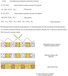
In recent years, due to the excellent characteristics of photopolymer recording materials such as high diffraction efficiency, high resolution and high signal-to-noise ratio, they have gradually emerged in volume holographic storage, fiber Bragg grating, waveguide, sensing and communication applications, and achieved a lot of significant results. Among them, a large number of acrylate photopolymers with stable performance, many kinds and low price have been studied. However, acrylate photopolymers have some defects, such as large shrinkage, small refractive index modulation and low stability. These problems hinder the expansion and further application of acrylate photopolymers. Based on the above research, the effects of various components in the photopolymer based on TMPTA double monomer system were studied, and a variety of photopolymer materials based on TMPTA double monomer system were compared in this paper. Combined with the diffusion movement of monomers, the effects of different film-forming resins, active monomers and photoinitiators on photopolymers were studied, and the ratio of materials was optimized. In technology, the system does not require solvent wet treatment. Just mix the medicine evenly and inject it into the mold prepared by two specific pieces of transparent glass. The thickness of the sample can be controlled by the gasket between the glasses, so it is easy to make a film with controllable thickness. Finally, bisphenol A epoxy resin and acrylate monomer TMPTA were selected in different double monomer systems. This is because the reaction activity of epoxy resin and acrylate monomer TMPTA is different, and the polymerization rate of TMPTA is much faster. When TMPTA molecules polymerize rapidly at the bright stripes, the epoxy resin is still colloidal and does not react, which is conducive to the diffusion of TMPTA molecules. Therefore, the two monomers can be separated from each other, resulting in a large refractive index difference. The network structure formed after TMPTA polymerization is combined with epoxy group to initiate epoxy group ring opening, and epoxy group is continuously inserted into it to realize chain growth, branching and crosslinking. A highly crosslinked stable structure is formed in the material. The photoinitiator is high reactive orange solid irgacure 784. Under the 532 nm laser, the ground state of irgacure 784 molecule absorbs photons rapidly, transitions to the excited state, and photodissociates. It forms a product state that is very transparent to visible light. In this system, irgacure 784 molecule first isomerized under the irradiation of coherent light to obtain the coordination unsaturated titanium central double free ground state. Then it initiated the free radical polymerization of TMPTA monomer. Finally, the ring opening polymerization of epoxy resin was carried out under the subsequent treatment. The material thus exhibits high stability and low shrinkage. By introducing double photoinitiators, the polymerization rate of active monomers was greatly accelerated, and the photosensitive sensitivity and photosensitive wavelength range of the system were improved. At the same time, the information is successfully recorded in polymer film samples, which proves that it has good holographic recording and high resolution performance. The holographic parameters are tested, which include diffraction efficiency of materials under different exposure intensity, exposure time and temperature. It shows that the double monomer system has better diffraction efficiency at exposure light intensity of 10~15 mW/cm2, time of 40~80 s and temperature of 46 ℃ than at the other conditions. The experimental results show that the system with good high temperature resistance manifests that the diffraction efficiency is up to 91.5% and the refractive index is more than 2.98×10⁻³, also, the transmittance is over 95.6%, which is under the conditions of a recording angle of 30°and a thickness of 70 μm. After 72 hours of high and low temperature cycling in the test chamber, the diffraction efficiency decreased to 87.2% and the decrease range was 4.7%. The temperature in the box is maintained at 80 ℃ and the humidity is 80 RH. The shrinkage of Bimonomer photopolymer system is only 0.504%.As a holographic recording medium, it can effectively record holographic information with high resolution and high diffraction efficiency. Due to the high diffraction efficiency and high stability of the polymer, the material is more suitable for other applications such as hologram and permanent storage of big data.
May. 25, 2022Vol. 51 Issue 5 0509001 (2022)
Zichao WEI, Yimin LOU, Juanmei HU, and Fengmin WU
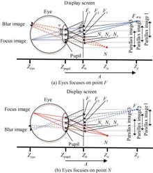
Recently, near-eye display technology has developed rapidly. Augmented reality, virtual reality, and other related products have begun to enter the field of mass consumption, bringing people a novel visual experience. However, while enjoying the visual feast, users have to endure traditional near-eye display technology defects, such as small angle of view, limited exit pupil area and resolution, easy to cause dizziness, and visual fatigue. To solve the above problems, researchers began to explore the application of holographic display, light field display, and retinal projection display technology to improve the visual effect of near-eye display and enhance the comfort of use. Among them, retinal projection display technology has attracted much attention because of its advantages of a simple solution, compact structure and easy integration.Retina projection display technology is based on the principle the of Maxwellian view. The human eye′ retina is used as a display screen, and a clear image is projected directly on it to avoid image blur caused by eye focusing. Using this method can effectively alleviate the problem of visual fatigue caused by the conflict of vergence and accommodation, but it has the disadvantages of small exit pupil diameter and inability to provide correct depth information. To overcome the above shortcomings, a partition and time-division multiplexing 3D retinal projection display technology using the principle of Maxwellian view is proposed.According to the human visual characteristics, the virtual scene is divided into an edge background area and a central gaze area. Time-division multiplexing 3D retinal projection display technology is used for the central gaze area to display the image group on the DMD at high frequency. At the same time, the point light sources in the LED array are controlled to illuminate synchronously according to the same time sequence, and the image group refreshed by the DMD are views corresponding to each viewing angle. These views are matched with the viewing angles corresponding to the illumination angles of the point light sources to form multi-view images for time-division multiplexing projection. When the frequency of the time sequence is high enough, an observation window with dense viewpoints can be formed at the exit pupil by using the visual persistence effect of the human eye. The human eye can feel the effect of continuous superposition of multi-view images at the exit pupil position, realizing a true three-dimensional display with monocular focusing depth information, and increasing the exit pupil area. In the edge background area, a short-focus lens and a liquid crystal display device are used to obtain a larger edge viewing angle, and a half mirror is used as an optical combiner to fuse the image information of the central gaze area and the edge background area.It can be seen from the 3D effects of the central gaze area that the system realized a true 3D retinal projection display with monocular focusing depth information. Afterwards, to achieve an accurate depth display, we calibrated the actual depth position of the 3D images using the virtual depth value set in the computer. By calibration, the relationship between actual and virtual depths is obtained, so that more accurate depth images can be achieved. In further experiments, we verified the effect of the partition display: 3D retinal projection technology was used in the central gaze area to obtain a true three-dimensional display with monocular focusing and defocusing effects. The LCD and short focus eyepieces were used in the edge area to achieve a wide viewing angle display, and the center and edge images were well fused. The total viewing angle of the system is about 32°, which can cover the effective field of view of the human eye, including a viewing angle of about 7° in the foveated region. For edge areas, our system can also flexibly set the required depth of the background area by controlling the distance from the short focal lens to the LCD. This system can effectively alleviate the problem of visual fatigue. It also reduces the amount of data required for 3D rendering, while improving the visual experience of the near-eye display system, and also has good application prospects.
May. 25, 2022Vol. 51 Issue 5 0511001 (2022)
Junhua YAN, Zijia HU, Deyan ZHU, Yang CHEN, Yin ZHANG, and Liqian YU
With the rapid development of space remote sensing technology, higher requirements are put forward for the compact structure and high resolution of the optical system. Among various optical system structures, compared with refraction and catadioptric optical systems, off-axis three-mirror optical systems have the advantages of high temperature stability, no chromatic aberration and central obstruction, wide wavelength range and compact structure. Off-axis three-mirror optical systems are widely used in space detection, astronomical observation, and other fields. Traditional spherical and aspherical surfaces have some limitations in correcting the non-rotationally symmetric aberrations produced by off-axis reflective systems, which reduces the resolution of the optical system. The freeform surface has multiple degrees of freedom, which can effectively improve the aberration correction capability and reduce the size of the optical system. With the advancement of digital control optical element processing technology, optical elements containing freeform surfaces are gradually applied to various optical systems. Applying freeform surfaces to off-axis reflective optical systems can greatly simplify the structure of the optical system, reduce wave aberration, and improve the resolution of the optical system.The design of freeform surfaces has become an important direction for the development of high-performance optical systems. In 2018, ZHAO Yuchen et al. designed an off-axis three-mirror optical system with the tertiary mirror as XY polynomial freeform surfaces. The average wave aberration RMS value of the optical system is 0.034 λ, and the image quality of the system is good. In the same year, LI Xuyang et al. designed an off-axis three-mirror optical system in which the primary and the tertiary mirrors are XY polynomial freeform surfaces, the optical system has an average wavefront aberration of 0.07 λ. In 2019, MENG Qingyu et al. designed a freeform off-axis three-mirror system with good imaging quality, the focal length of the system is 1 000 mm. The primary mirror and the tertiary mirror are both XY polynomials freeform surfaces, the wave aberration RMS value of the optical system is 0.04 λ (λ=0.633 μm). In 2019, WU Weichen et al. designed an off-axis three-mirror optical system based on freeform surfaces. The optical system works in the long-wave infrared band with a focal length of 9.3 mm, and the image quality is close to the diffraction limit. In 2020, CAO Chao et al. designed an off-axis three-mirror optical system based on XY polynomial freeform surface, the transfer function is close to the diffraction limit. At present, freeform surfaces have been widely used in focusing optical systems, but their applications in the field of afocal optical systems are relatively few. The afocal system uses parallel light to enter and exit, and the focal length is infinite. It can be used as a beam-reducing system to reduce the size of subsequent optical elements, reduce costs, and save materials. Further exploration and research on off-axis three-mirror afocal optical systems based on freeform surfaces are needed. The initial structure of off-axis reflective optical systems has become a hot and difficult point in optical system research. At present, methods to solve the initial structure such as Simultaneous Multiple Surface (SMS) method, Partial Differential Equation (PDE), and Construction-Iteration (CI) method are all used in off-axis reflective imaging systems. However, the existing design methods for off-axis reflective afocal optical systems are based on the coaxial structure, this design method cannot directly design the initial structure of the off-axis reflective afocal system.In this paper, a design method of the compact off-axis three-mirror afocal optical system is proposed. Based on parameter requirements the compact off-axis three-mirror afocal optical system model is constructed. The secondary mirror and the tertiary mirror have tilt angles relative to the optical axis, the relationship between the parameters in the model is established and the value ranges of the parameters are got. The influence of optical parameters on the structure of the optical system is analyzed, the initial structure of the off-axis three-mirror optical system is established. At present, Zernike polynomial freeform surfaces and XY polynomial freeform surfaces are widely used in off-axis reflective optical systems. Compared with XY polynomial freeform surface, Zernike polynomial freeform surface can correspond to wave aberration, which is convenient for the optimization design and easy to process, detect, and assemble. In this paper, Zernike polynomial surface is selected as the mirror freeform type to optimize the initial structure. The design of aperture off-axis and field of view off-axis three mirror optical system with the infrared band φ600 mm envelope, entrance pupil diameter of 350mm, and a compression ratio of 7 times are completed. The secondary mirror and the tertiary mirror of the field of view off-axis three-mirror optical system have an inclination angle, while the aperture off-axis three-mirror system has no inclination angle. The design results show that the wave aberrations of the two optical systems are less than 0.1 λ (λ=3.7 μm) in each field of view. For the designed optical system, tolerance analysis is an important step in evaluating the feasibility of the optical system. Tolerance values of the optical system are reasonably allocated and Monte Carlo analysis is performed to simulate the actual processing conditions. Tolerance analysis shows that the probability of wave aberration less than 0.08 λ for the aperture off-axis three-mirror system reaches more than 90%, and the probability of wave aberrations less than 0.07 λ for the field of view off-axis three-mirror system reaches more than 90%, indicating the effectiveness and rationality of the optical system design. The comparison of the two systems shows that the field of view off-axis three-mirror optical system can make the structure more compact and the wave aberration smaller, which verifies the feasibility of the initial structure design method of the optical system proposed in this paper, and meet the practical application requirements of compact structure and high resolution.
May. 25, 2022Vol. 51 Issue 5 0511002 (2022)
Huiji WANG, Nan LI, Xuankui LI, Cheng ZHOU, and Lijun SONG
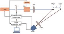
Different from traditional optical imaging technology, correlated imaging uses a single-pixel detector and a spatial light modulator to reconstruct object image information based on correlation calculations, having the characteristics of super-resolution, non-local, and anti-interference. Time-of-flight (TOF) technology is an effective method for optical remote sensing and three-dimensional imaging of target recognition. Compared with traditional laser correlation imaging, 3D correlation imaging can not only obtain the two-dimensional light field intensity information of the target object, but also effectively obtain the longitudinal distance information between the target objects, so that the size and position of the imaging target can be quantitatively analyzed. Three-dimensional correlation imaging technology mainly includes steroscopic vision and TOF imaging technology. To improve the image reconstruction quality of intensity 3D correlation imaging, this paper employs differential correlation imaging reconstruction algorithm and TOF technology, and the theoretical formula of intensity correlation 3D imaging is deduced. The working mode is that the short-pulse laser forms pseudothermal light through the rotating frosted glass. After passing through the beam splitter, one of the beams irradiates the target object to be measured and then is received by the Photomultiplier Tube (PMT); the other beam is detected by the array detector. The high-speed data acquisition system digitizes the peak light intensity signal detected by the PMT into discrete data points, uses the TOF technology to divide the detection signal into slice signals of different time (distance), and then integrates the signals in the respective slices to obtain the slice signal detection value, and finally the DGI algorithm is used to perform two-dimensional correlation imaging reconstruction calculation for each slice signal separately. This paper mainly investigates the influence of the light source laser power and reconstruction algorithm parameters on the imaging quality in the pseudo-thermo-optic 3D correlation imaging. The imaging results of two flat objects to be measured (the front-end target is a four-pointed star and the back-end target is the letter F) with a distance of 80 cm and a resolution of 200 pixel × 200 pixel in the numerical simulation are given. Among them, the simulation pulse laser uses the function p(t)=exp-τ2/σ2 , the detection times is 20 000, and the sampling rate is 50%. In order to further verify its effectiveness, a pseudo-thermo-optical 3D correlation imaging experimental system is built. This paper uses a 532 nm pulsed laser as the light source and frosted glass as the spatial light modulator to build a set of pseudo-thermal light three-dimensional correlation imaging experimental system, which realizes the three-dimensional image reconstruction of a 200 pixel×200 pixel target object with a longitudinal distance of 60 cm at an absolute distance of 5.5 m in the laboratory environment. The reconstructed 3D slice images that are lower than the set threshold parameters in the simulation and experimental results are reset to zero, thereby reducing the influence of the background noise of other slice images on the quality of the reconstructed images during the 3D correlation imaging stacking process. Within a certain threshold parameter range, appropriately increasing the threshold parameter can effectively improve the reconstruction quality of 3D correlated imaging images. To further investigate the performance of the 3D correlation imaging experimental system, experimental tests are carried out for 3D correlation imaging under different laser powers, respectively. The experimental verification shows that by properly increasing the power of the laser light source, the influence of the time jitter of the echo signal on the reconstructed image quality can be effectively suppressed, and the longitudinal distance reconstruction quality and measurement accuracy of the 3D image can be further improved. The work has a reference significance for promoting the application of intensity 3D correlation imaging technology in the field of lidar imaging.
May. 25, 2022Vol. 51 Issue 5 0511003 (2022)
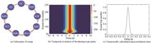
Li YAN, Qimeng LIN, Yuanqi SONG, Xuzhuo JIA, Jianing TAO, Yangyang LI, Pengye SONG, and Man JIANG
Passive mode-locked fiber lasers have potential applications in fiber optic communication, fiber optic sensing, optical frequency measurement, and aerospace due to their good beam quality, compactness, small size, low fabrication cost, tunability, and easy generation of ultrashort pulses. In recent decades, several types of mode-locked pulses can be generated using passive mode-locked fiber lasers, such as Gaussian pulses, self-similar pulses, soliton pulses, noise-like pulses, and so on. Among them, noise-like pulses is a special pulse generated by mode-locked lasers under certain conditions, which is widely used in low-coherence spectral interferometry, micromachining, nonlinear frequency conversion and supercontinuum spectrum generation due to its wide pulse width, high energy, and low time-domain coherence. In light of these applications, broadband noise-like pulse generation in erbium-doped fiber lasers has attracted considerable interest. The study of noise-like erbium-doped fiber lasers based on passive mode-locking technique has been reported extensively. Researchers have mostly used longer gain fibers or single-mode fibers to adjust intracavity dispersion and accumulate nonlinearity as a way to obtain the output of noise-like mode-locked pulses. So far, it has not been reported that using highly nonlinear fiber based on nonlinear polarization rotating mode-locking mechanism to manage the nonlinear in laser cavity to realize the mode-locked fiber laser with wide spectrum. In this work, we experimentally report the noise-like pulses generation in an anomalous dispersion erbium-doped fiber laser based on nonlinearity management technique. The erbium-doped mode-locked fiber laser adopt nonlinear polarization rotation technique. In the experiment, by introducing dispersion compensating fiber and highly nonlinear fiber into the nonlinear polarization rotation mode-locked erbium-doped fiber laser resonator, intracavity dispersion and non-linearity management is achieved, resulting in a stable mode-locked pulse output. When the intracavity highly nonlinear fiber length is 6 cm, corresponding to a net cavity dispersion of about -0.019 ps2. An ultrashort pulse output with a central wavelength of 1 534 nm, a pulse width of 1.9 ps, a repetition frequency of 20.1 MHz, and a 40 dB spectral bandwidth of about 100 nm can be obtained. Based on this, the length of the highly nonlinear fiber in the cavity is increased to 30 cm, and the total dispersion in the cavity is -0.021 ps2. This laser system can achieve noise-like pulse operation by properly adjusting the state of the wave-plate when the pump power is 1 100 mW. The output spectral coverage range of noise-like pulse is 1 280-1 850 nm, the bandwidth of 40 dB is 500 nm, the peak pulse width is as short as 70.9 fs, the base pulse width is 26.6 ps, and the repetition rate is about 19.7 MHz. The maximum output power is 2.08 mW at pump power of 1 100 mW, corresponding to an optical conversion efficiency of 0.18%. In order to verify the power stability of the noise-like mode-locked fiber laser, we monitor its output power for 2 hours, and the monitoring results showed that the output power is always maintained at about 1.01 mW, and the root mean square is calculated to be 1.14% for 2 hours, indicating that it has good environmental stability. After obtaining noise-like mode-locking pulses, we investigate the output spectra and the corresponding autocorrelation curves of noise-like pulses at different pump powers. It is found that the duration of the spike pulses decreased slightly with increasing pump power, a feature that mainly stems from the fact that the spectral bandwidth becomes progressively wider. Conversely, as the pump power increases, the pulse width of the base becomes progressively wider. And as the pumping power increases, the shape of the spectrum remains essentially the same and the output spectrum broadens in both the short and long wavelength directions, gradually increasing the spectral coverage. This is mainly due to the increasing power coupled into the highly nonlinear fiber as the pumping power increases. The present experimental study will allow subsequent optimisation of the fusion loss of the highly nonlinear fiber by tailoring the fibre device for wide bandwidth operation and selecting a higher power pump laser, resulting in a wider spectrum of noise-like mode-locked pulse output. The research in this paper provides a feasible solution for preparing a broad-spectrum noise-like mode-locked laser light source, which has great potential for applications due to its compactness, stable output, and ease of fabrication.
May. 25, 2022Vol. 51 Issue 5 0514001 (2022)
Min CHEN, Gaofang YIN, Nanjing ZHAO, Tingting GAN, Mengyuan GU, Peilong QI, Zhichao DING, Lu WANG, Chun FENG, and Xiaoling ZHANG
The photosynthetic fluorescence parameters of algae are easy to measure and sensitive to external stress. It is an important indicator of water quality biological toxicity measurement. However, different toxicity test schemes would lead to great differences in the toxicity data, and the stability and comparability were uncertain. Since fluorescence dynamics technology for measuring photosynthetic fluorescence parameters essentially uses optical detector to monitor the change of chlorophyll fluorescence signal in microalgae. In this paper, the concentration of chlorophyll was used as the measurement of biomass, and Chlorella pyrenoidosa was used as the test object to analyze the relationship between photosynthetic fluorescence parameters as the end point of toxicity test and the initial biomass of toxicity test algae samples under short-term exposure (1 h and 3 h) of diuron. The results showed that: 1) When the initial biomass changes, the correlation between photosynthetic fluorescence parameters and biomass would directly affect the stability of the toxicity test results. The photosynthetic fluorescence parameters could be divided into two categories. The first category was Fv/Fm, Yield, α, rP, σPS II and τes, whose values were not related to biomass changes and only represented the photosystem information of Chlorella pyrenoidosa. The toxicity test results obtained by these parameters were not affected by the change of initial biomass. When the initial chlorophyll concentration changed in the range of 20~1 000 μg·L-1, 10 μg·L-1 diuron stress for 1 h and 3 h, the average values of the corresponding relative standard deviations of the six parameter test results were 2.74% and 3.12% respectively, and the toxicity test results were stable. The second category of parameters was Ek, F0, Fm, Fv and JVPⅡ. Their values were affected by biomass and contain biomass information. Among them, Ek was negatively correlated with chlorophyll concentration, and F0, Fm, Fv and JVPⅡ were positively correlated with chlorophyll concentration. The toxicity test results of these parameter were obviously affected by biomass fluctuation and their stability became worse. When the chlorophyll concentration changed in the range of 20~1 000 μg·L-1, the average values of relative standard deviation of the five parameter test results under 10 μg·L-1 diuron stress for 1 h and 3 h were 14.66% and 17.27% respectively. 2) The Logistic model was selected for dose-effect analysis, and the photosynthetic fluorescence parameters Fv/Fm, Yield, α, rP, σPSⅡ, τes, F0, Fm and Fv could establish a good dose-effect relationship with diuron. According to EC50, EC20 and correlation coefficient R2, the optimal range of initial chlorophyll concentration of algae when photosynthetic fluorescence parameters were used as the end point of toxicity test were given. For parameters Fv/Fm, Yield, α, rP, σPSⅡ, and τes, due to population dependence, too low biomass would affect the photosynthetic physiological state of algae species, the recommended initial chlorophyll concentration range was 10~2 000 μg·L-1; for parameters F0, Fm and Fv, more sensitive toxicity test results (lower EC20) could be obtained due to higher initial biomass, the recommended range was 200~1 000 μg·L-1. This result provides an important basis for the establishment of a rapid detection method for water quality biological toxicity based on algal photosynthetic fluorescence parameters, and will be helpful for ecological risk assessment of the aquatic environment.
May. 25, 2022Vol. 51 Issue 5 0517001 (2022)

Lei SUN, Yipeng LIAO, Kunhua ZHU, and Xin YAN
The field emission electron source has a wide range of application value in the field of vacuum electronics, and the realization of the uniformity and patterning of the in-situ growth of the emitter material is the key technology. The traditional patterning process is complicated and the pattern has not been carefully designed, resulting in uneven electric field distribution. This paper uses ANSYS Maxwell 16.0 simulation software to study the law of electron motion trajectory, and proposes a new idea of the effective emission size of the graphical emitter array and the cathode structure of the optimal array spacing to improve the field emission performance. The simulation results show that when the array spacing d is 200 μm, the electric field distribution in the central area of the patterned array is flat, and the surrounding area of the array rises abruptly. This is mainly due to the fact that the edge part of the array exhibits the characteristics of a needle tip more than the central part of the array. When d is smaller, the field strength of the edge area between the unit arrays is superimposed, and a field strength superimposition area appears. When d slowly increases, the edge superposition effect of the field strength is weakened, and the electric field shielding effect is also weakened. Therefore, when d is larger (400 μm), the field strength of the cathode surface tends to be flat, because the edge superposition effect of the field strength and the electric field shielding effect are balanced. However, as d increases to a certain extent, when the array spacing is 600 μm, the center position of the cell array plane can be relatively far away, the field emission of the cell array is relatively independent, and the electron emission has a neutral area. It can be seen that when d is selected at a moderate value, the superposition effect of the field strength at the edge of the array is weakened, and there will be no blind areas in the surrounding electric field, and the electric field basically achieves a uniform distribution. Subsequently, according to the simulation results, the patterned seed layer is accurately positioned by inkjet printing, and then the ZnO nanorod array is hydrothermally grown. Field emission test results show that as d increases, the turn-on field strength Eon decreases from 2.95 V/μm at 200 μm to 0.57 V/μm at 400 μm, and further changes to 2.26 V/μm at 600 μm. The enhancement factor b increases first and then decreases as d increases from 200 μm to 600 μm. This is consistent with the simulation results, that is, when the effective emission size of the ZnO cathode array is 200 μm, when d is 400 μm, the field emission performance is optimal, and its turn-on field is 0.57 V/μm, and the field emission enhancement factor is 32 179. Combining the high efficiency of graphic design and inkjet printing, it is expected to realize a high-performance field emission electron source.
May. 25, 2022Vol. 51 Issue 5 0525001 (2022)
Xuquan WANG, Hongyi WANG, Yonggang ZHANG, Songlei HUANG, and Jiaxiong FANG
With the advantages of speediness, lossless and high-efficiency, the technology of Near-infrared (NIR) spectroscopy can be applied to the applications of composition analysis. In recent years, the development of portable micro-spectrometer and spectral sensing Internet of Things has promoted the application of spectral analysis technology to field analysis and online detection. The NIR spectral sensors with High Dynamic Range (HDR) and anti-interference capability are required. Digital Readout Circuit (DROIC) can optimize the quality of readout signal and improve the performance of NIR focal plane array effectively. Pulse Frequency Modulation (PFM) DROIC can convert the photocurrent of detector into digital pulses by resetting the integrating capacitor repeatedly in integrating period. PFM structure is a feasible technique for HDR DROIC, because it breaks the limitation of charge capacity determined by integrating capacitance and power supply voltage in conventional readout circuits. Due to process limitations, the residual charge on integrating capacitor after the last reset cycle can cause conversion errors. In addition, there are some problems such as poor linearity under strong light environment. Various methods have been proposed to resolve the problems of linearity and conversion errors. InGaAs Focal Plane Arrays (FPAs) have the advantages of working near-room temperature, high detection rate, good uniformity and stability, which is beneficial to realize the miniaturization design of the NIR photoelectric system. Most InGaAs detectors use the Capacitance Feedback Trans-impedance Amplifier (CTIA) input stage, but there are relatively few researches on the PFM ROIC of CTIA input stage currently.A two-step Residual-time-counting Pulse Frequency Modulation (RTC-PFM) DROIC was proposed for CTIA input stage of InGaAs FPAs to improve the dynamic range. The non-ideal reset of CTIA input stage in PFM DROIC is studied. The PFM conversion theory model of CTIA input stage is established. The conversion error caused by residual charges of integral capacitor and the non-linearity caused by reset missing charges are analyzed in detail. Theoretical analysis shows that the conversion error caused by residual charges is more obvious only in the case of small integral current. On the contrary, the non-linearity of the conversion values caused by the missing charge gradually deteriorates with the increase of the integral current.A two-step RTC-PFM digital structure with double integral capacitances was designed for 256×1 linear spectral sensor. With the improvement of conversion error, the fusion of 16-bit rough conversion and maximum 16-bit fine conversion is realized. The coarse conversion is accomplished by pulse counting and the fine conversion is implemented by time counting of high frequency clock. In order to improve the non-linearity caused by the missing charges, the most direct measure is to reduce the reset times. The DROIC adopts 50 fF (Cmin) and 1 pF (Cmin+Cmax) integrating capacitors, which can be chosen by an external signal SEL. In low light mode, a small integrating capacitor is used to improve the conversion accuracy. In strong light mode, a larger integrating capacitor is used with the purpose of control the number of integration-reset times, which is related to non-linearity of conversion. At the same time, the residual time counting two-step structure can ensure high resolution performance even with large integrating capacitance. The simulation results show that the actual converted characteristics are consistent with the theoretical analysis. The actual converted values show very typical logarithmic properties due to the effect of the reset charge loss. The comparative analysis proves that the precise time counting can obviously reduce the conversion error caused by the residual charge of the integral capacitor. In the simulation, the non-linear degree of conversion value is 0.62% and 0.06% respectively when the small integrating capacitor and the large integrating capacitor are used in the large integrating current. The linearity is significantly improved when the large integrating capacitor is selected. Furtherly, the layout of RTC-PFM DROIC unit was implemented with the size of 90 μm×200 μm.This paper firstly introduces the non-ideal reset of PFM DROIC and established the PFM conversion theory model of CTIA input stage. In order to improve the conversion accuracy and linearity, a RTC-PFM DROIC was proposed for CTIA input stage of InGaAs FPAs. With the fusion of rough conversion and fine conversion, RTC-PFM DROIC can get a performance boost on conversion accuracy. The analysis and simulation show that it is beneficial to field application of short-wave infrared spectral sensors.
May. 25, 2022Vol. 51 Issue 5 0525002 (2022)
Bozhao FAN, Yutao FENG, Quan WANG, Chi GAO, Yang WU, Bin HAN, Chenguang CHANG, Juan LI, Yiru LI, Hengxiang ZHAO, and Di FU
Spatial Heterodyne Raman Spectroscopy (SHRS) is a new type of Raman spectroscopy detection technology, which has the advantage of high throughput, high spectral resolution, high sensitivity and no moving parts. SHRS can meet the high-sensitivity detection requirements of weak Raman scattered light, and can also obtain clear and sharp Raman spectra. For Raman spectrometers, fluorescence is an inevitable background signal. The fluorescence intensity and the Raman intensity are approximately inversely proportional to the fourth power of the wavelength, so the excitation wavelength of near-infrared light has lower fluorescence than visible light. The excitation wavelengths of near-infrared light are mostly 785 nm, 830 nm and 1 064 nm, of which the shorter 785 nm has larger fluorescence. Although the 1064 nm excitation light has a weaker fluorescence, it requires the near-infrared InGaAs focal plane. Compared with visible detectors, it has higher noise, lower sensitivity and resolution. Therefore, this article chooses the wavelength of 830 nm as the excitation light for Raman spectroscopy detection, and its fluorescence is lower than that of 785 nm. On the other hand, the visible detectors can be used for high-sensitivity detection. For the excitation wavelength of 830 nm, this paper designs, simulates, develops and tests SHRS. The Littrow wavelength of the spectrometer is 842 nm, the theoretical spectral sampling interval is 2.96 cm-1, and the theoretically Raman shift range is 171.71~3 031.04 cm-1. The spatial heterodyne interferometer adopts integrated adhesive technology. To increase the throughput, the field-widened prisms are added to the interferometer. The field angle tolerance of the interferometer is selected to be ±2° to ensure the contrast of the interferogram in actual work, and the corresponding contrast of the ideal interferogram is better than 0.98. The fringe-imaging lens group selects a double telecentric lens group with a magnification of 1. The telecentric configuration guarantees the uniform illumination of the image surface, and the symmetrical structure can effectively balance aberrations and further enhance the stability of the system. A checkerboard target is used to test the processed fringe-imaging lens group. The measured average magnification is 1.001 9 and the relative distortion is 0.19%. The Kr lamp is used as the input light of the system to verify the design parameters of the SHRS prototype. According to the positions of the two spectral lines 877.675 nm and 892.869 nm of the Kr lamp and the corresponding Raman shift, the actual spectral sampling interval is 2.918 2 cm-1. The smaller value compared with the design value is mainly due to the dispersion of the field-widened prism. The actual Littrow wavelength is 841.95 nm, which is close to the theoretical value. The detector selected in this paper does not respond to light with a wavelength greater than 1 000 nm, so the actual Raman shift range is 171.01~2 048.19 cm-1. The design parameter and the simulation of the system are verified. In the Fourier transform of the interferogram to the spectrogram, apodization is needed to suppress the side lobes, and different apodization functions have different degrees of spectral line broadening, resulting in different actual spectral resolution. In rectangular function apodization, the spectral resolution is about 1.207 times the theoretical spectral sampling interval. The effective spectral resolution of the SHRS prototype is 3.35 cm-1. An important parameter to measure the performance of Raman spectrometer is the Signal-to-Noise Ratio (SNR) of the Raman spectrum. We choose the peak intensity of the Raman spectrum after removing the baseline as the signal intensity, and the standard deviation after removing the baseline from the Raman spectrum peak area as the noise, and use the ratio of the two as SNR of the measured Raman spectrum. In the experiment, the excitation light power is 500 mW, and the integration time is 10 s. First, the standard Raman sample cyclohexane is tested. SNR of the main Raman peak at 795.5 cm-1 is 913, and SNR of the weakest Raman peak at 1 341 cm-1 is 15. It can be verified that the SHRS prototype has good Raman spectrum measurement capabilities, as well as high sensitivity and SNR. Secondly, the solid samples calcium carbonate, calcium sulfate and potassium sulfate are tested. These samples are all strong Raman active substances, and the Raman spectrum peaks of various substances can be accurately identified, and SNR of the main Raman spectrum peaks is greater than 300. Finally, experiments are carried out on 75% alcohol solution, glycerin and glucose powder. The Raman activity of these samples is relatively weak, and there are obvious baselines in the measured Raman spectra, indicating that there is a certain fluorescent background in the spectra. However, a clear and accurate Raman spectrum is still obtained, and the main Raman spectrum peaks of various substances can be accurately obtained, and SNR of each spectrum peak is greater than 20. In general, SHRS has higher detection sensitivity and better stability and can meet the analytical requirements of Raman spectroscopy detection. It has certain advantages in the Raman detection of high-fluorescence background substances and has certain development potential in biomedicine, food safety, geological prospecting, planetary exploration, etc.
May. 25, 2022Vol. 51 Issue 5 0530001 (2022)
Zhuo MA, Yafei LI, Yang LU, Fang SONG, Chuantao ZHENG, and Yiding WANG
China is not only a large agricultural country, but also one of the countries suffering from the most serious agricultural disasters in the world. Early fire detection can help to avoid greater losses. Crops have a period of smoldering before the open flame. Due to lack of oxygen, the combustion is extremely insufficient, and a small amount of carbon monoxide (CO) with a relatively stable concentration will be produced. Therefore, the occurrence of early fire can be judged by detecting gas-phase CO. Non-Dispersive Infrared (NDIR) absorption spectroscopy was used in this paper. Based on the absorption band of CO gas molecules at 4.6 μm, a differential infrared CO sensor system for early fire detection was developed by using a broadband infrared thermal light source and a dual-channel pyroelectric detector. This sensor system is mainly composed of a gas pretreatment part, an optical part, an electrical part and an upper computer monitoring part. Firstly, the detection principle of the sensor system was introduced, and then the absorption band of CO in the infrared region was selected by comparing the strength of absorption lines in different absorption bands and excluding the absorption interference of other gas molecules. Through the derivation of the optical matrix, the structure of the gas cell was designed and optimized, and the optical path of gas absorption reached 180 cm . The background noise fluctuation range of the phase-locked amplifier is 38.89 μV~43.23 μV, and the lowest detection limit is 0.15 μV. Finally, the performance of the sensor system was tested through related experiments. The results show that the measurement resolution is less than 2×10⁻⁵ and the response time is 35~38 s. The concentration level of the 0×10-6 CO standard gas sample was dynamically monitored for 80 minutes, and its concentration fluctuation range is -1.42×10⁻⁵~1.51×10⁻⁵. When the integration time is 0.25 s, the detection limit of the system is 1.54 ×10⁻⁶, and when the integration time is 300 s, the detection limit of the system can reach 3.50×10⁻⁷. Kalman filtering algorithm was used to improve the stability of the system. Similarly, the 0×10-6 CO standard gas sample was dynamically monitored for 80 minutes. The results show that the relative error is reduced by 40.56 %, and when the integration time is 0.25 s, the detection limit is reduced to 3.60×10⁻⁷. Finally, fire smoldering experiments of cotton, paper and wood were carried out to study the relationship between CO concentration and smoldering time. It is proved that the change of CO concentration can be used to detect the occurrence of fire. The experimental results show that the CO sensor system has a good early fire detection capability and wide application prospects.
May. 25, 2022Vol. 51 Issue 5 0530002 (2022)
Peng WANG, Fanchang MENG, Zili ZHANG, Dezhao WANG, Shan WANG, Entao YAO, Lei WANG, and Ruiqian YE
2D/3D integrated circuit packaging technology is adopted in the process of wafer packaging and this technology uses wafer bumps to connect active devices. Inconsistent bump heights will cause circuit break after packaging, which will cause the whole chip to fail. Therefore, on-line detection of the height consistency of bumps is required during wafer packaging. To meet the above requirements, a fast and high-precision bump height measurement method based on optical triangulation method is studied. Based on the basic principle of oblique incidence optical triangulation method, the line beam is projected onto the chip bump, and the reflected beam on the chip surface is collected by the camera after through the imaging system. The height of the bump is calculated according to the geometric characteristics of the light stripe in the image collected by the camera and the distance between the spot on the top of the bump and the light stripe. Compared with spectral confocal method and white light interferometry, this method has the advantages of high speed and high measurement efficiency, and can meet the needs of on-line measurement of chip packaging defects. When calibrating the parameters of the chip bump height measurement system, in order to solve the difficult problem of angle calibration of projection and imaging device in the traditional triangulation method, a new calibration method is adopted: the magnification and pixel height ratio of the imaging system are used to replace the device angle to realize the indirect calibration of angle parameters. In order to accurately calibrate the pixel height ratio, a laser interferometer is used to accurately measure the height deviation of the reference plane. The center coordinate of the light strip on the reference plane is extracted by the gray centroid method to obtain the center offset of the light strip. The pixel height ratio is calculated according to the center offset of the light strip and the height deviation of the reference plane. A high-precision circular calibration plate is used to calibrate the magnification of the imaging system. The Hough circle transformation algorithm is used to extract the center coordinates of the circular pattern, and the magnification of the imaging system is calculated according to the ratio of the center distance of adjacent circles in the image to the actual distance. By substituting the calibrated system parameters into the measurement model, the accurate measurement of chip bump height can be realized. Using this method, the chip bump height is measured, and the standard deviation of height measurement is 0.58 μm. If the same bump is measured repeatedly, the extension uncertainty is less than ±1 μm. The experimental results show the accuracy of the measurement method. Compared with the traditional optical triangulation method, the chip bump height measurement model proposed in this paper is not affected by the light strip position and width, and the measurement accuracy and speed have been further improved. The research results of this paper are of great significance to realize the rapid and accurate detection of chip bumps, and have a strong reference value for the height measurement of objects with spherical structure at the top. This measurement method combined with high-precision mobile platform can further measure the bump height of chip or wafer, so as to evaluate the bump height consistency. Therefore, this measurement method has important application value for the research of industrial on-line bump height consistency measurement system.
May. 25, 2022Vol. 51 Issue 5 0512001 (2022)
Fen TAO, Lian XUE, Shangyu SI, Zhongliang LI, and biao DENG
The synchrotron is a machine which is used by physicists to produce high energy charged particles. The centripetal force acting on the relativistic electrons causes them to radiate electromagnetic radiation predominantly in vacuum ultraviolet and soft X-ray regions. The synchrotron radiation facility is a large, expensive, and complex organization, devoted to the provision of electromagnetic radiation to a wide range of experimental rigs, and service a community with diverse scientific backgrounds. Synchrotron radiation has the characteristics of high photon brilliance, high collimation and high purity. Double crystal monochromator is the core splitter in synchrotron radiation beamline. The diffraction beam produced by it contains fundamental and harmonic X-rays. As monochromators select from a given spectrum a series of harmonics whose wavelengths satisfy Bragg's law for the monochromator diffracting planes, higher-order harmonics are still present in the spectrum after monochromatization with not negligible relative intensities. On the one hand, higher harmonics can reduce the monochromaticity of X-ray; on the other hand, higher harmonics have the characteristics of high resolution and high energy. In experiments, higher harmonics are usually used or suppressed according to the demands. High purity harmonics are obtained and fundamental waves are filtered by aluminum sheets of different thickness. Based on the characteristics of higher harmonics, the absorption spectrum, imaging and diffraction experiments are carried out on test beamline (09B) at Shanghai Synchrotron Radiation Facility (SSRF), which expanded the spectrum range and applications of synchrotron radiation at wavelength measurement.The lower limit of monochromator energy is an important feature for beamline. The lower limit of the monochromator energy in SSRF Beamline is 2 keV. There is no simple method to measure the lower limit of the monochromator energy at present. The lower limit of the monochromator energy can be easily measured by high order harmonic. The lower limit of 4.219 keV energy of Si(111) monochromator crystal is calibrated by measuring the K-edge absorption of element Se for third-order harmonic at 12 keV.Monochromaticity is an important criterion of beamline at synchrotron radiation, and thermal deformation of monochromator crystal affects photon energy bandwidth. The energy bandwidth of Si(333) crystal planes is 0.37"@30 keV. This value is on the same order of magnitude with the result of thermal deformation of crystal. It can be used in the detection of thermal deformation of crystal. The specular distortion of Si(333) lattice surface diffraction caused by thermal deformations of crystal Si(111) is studied by diffraction imaging with 12 keV higher harmonic.The ultrahard multifunctional X-Ray beamline in the phase II of SSRF with a photon energy range of 30~120 keV, with Laue diffraction monochromator to select from a given spectrum. It is necessary to characterize it at wavelength measurement by high-energy X-rays in this range. The rocking curve of high-energy Laue crystals is measured by Laue diffraction with 60 keV higher harmonic.Based on the test beamline at Shanghai Synchrotron Radiation Facility, studying the applications using higher-order harmonic of crystal monochromator in three aspects. First, the lower limit of the energy of the double crystal monochromator is calibrated. Second, the thermal deformation of crystal is directly observed by X-ray imaging. Third, Characterization of rocking curves of Laue crystal monochromator at high energy. Utilizing monochromator higher-harmonics, a variety of high-precision detections has been successfully realized. This work extended the applied range of Test Beamline at Shanghai Synchrotron Radiation Facility.
May. 25, 2022Vol. 51 Issue 5 0512002 (2022)
Wenjing XU, Jie CHEN, Zhangqu KUANG, Li ZHOU, Ming CHEN, and Chengbin ZHANG
The 4T Pinned Photodiode (4T-PPD) active pixel is the most widely used pixel structure for CMOS Image Sensor (CIS). In recent years, as the application of CIS has gradually expanded to the Internet of Things (IoT) and Artificial Intelligence (AI) fields, there is an increasing demand for low energy consumption. The basic theory and commonly adopted approach to reduce power consumption are to lower the power supply voltage, while the supply voltage of 4T-PPD is traditionally greater than 2.8 V. In 2016, the study published in JSSC suggested that by improving the timing, the 4T-PPD active pixels could work at 0.9 V, but the readout noise was as high as 83e-rms and the dynamic range was only 50 dB, which could only meet low-quality imaging.Several studies have been conducted on the charge transfer characteristics of traditional high-voltage 4T-PPD. In 2003, FOSSUM E R simulated the charge transfer from PPD to Floating Diffusion (FD) node based on thermionic emission theory. Based on this work, in 2016, HAN Liqiang et al. included non-ideal factors such as the reverse charge injection from FD to PPD. Additionally, in 2019, CAPOCCIA R et al. added an estimate of the thermionic emission barrier height based on the findings of the aforementioned studies. However, these theories were not fully applicable to low-voltage 4T-PPD, since they all assumed a complete photo-generated charge transfer inside the PPD. When the voltage drops, the electrons far away from the transfer gate lack a lateral electric field and stay in the photosensitive area, causing image lag, which will seriously affect the imaging quality.In this paper, a low-voltage 4T-PPD active pixel was designed. First, a theoretical analysis of the internal charge transfer mechanism of PPD was proposed. Three charge transfer mechanisms operate inside the PPD, namely thermal diffusion, self-induced drift, and fringe-field drift. As the charge transfer by fringe-field drift is much faster than thermal diffusion or self-induced drift, the charge transfer time inside the PPD depends predominantly on the distance where the fringing field is absent. According to the derived equations, when the photogenerated charge to the full-well chargeis less than 4%, thermal diffusion is the main mechanism for the no-fringing-field section, and the length of the no-fringing-field section is almost the same. When the photogenerated charge to the full-well chargeis larger than 4%, self-induced drift is the main mechanism for the no-fringing-field section. Moreover, when the transfer gate voltage increases, the length of the no-fringing-field section becomes shorter. As the PPD size decreases, the length of the no-fringing-field section becomes shorter significantly.When the transfer gate voltage drops, the electrons far from the transfer gate lack fringing field and could not be pulled out of the PPD within transfer time, thus resulting in image lag. To solve image lag caused by low-voltage 4T-PPD, and easily achieve it without changing the process steps and conditions, the shape of the PPD layer might be changed. In previous studies, triangle, W-shape, trapezoid, and L-shape PPD have been reported, but all these designs aim at large-sized pixels. For small-sized pixels, the PPD layer should not be cut too much, otherwise, it would affect the full-well capacity and reduce the dynamic range. Therefore, a five-finger pixel layer was proposed to replace the traditional square pixel layer. Compared with conventional rectangular PPD, the five-finger shaped PPD not only reduces the length of the no-fringing-field section but also creates an extra electrical field in the direction of the charge transfer by the narrow width effect. This causes more electrons to be pulled out of the PPD. The proposed five-finger shaped PPD not only can accelerate the electrons transfer from PPD to TG but also meets the requirements of full-well capacity and dynamic range due to the small cut-off area.A prototype sensor was fabricated using a 0.11 µm 1P3M CMOS process. The experiment results show that the residual charge of the designed five-finger 4T-PPD is reduced by 80% compared with the traditional rectangle pixel. The performance of the designed five-finger 4T-PPD with 1.5 V voltage supply is as follows, the full well capacity is 4 928e-, the dynamic range is 67.3 dB, and the random noise is only 1.55e-rms, which are comparable to traditional high-voltage 4T-PPD. The findings presented in this paper provide important guidance for the design of low-voltage 4T-PPD.
May. 25, 2022Vol. 51 Issue 5 0523001 (2022)
Zhuang LIU, Qidong WANG, Haodong SHI, and Libo CHENG
Liquid crystal phased array can be widely used in space laser communication, space laser ranging and other fields. A phased array device is a diffractive optical device, which has the function of dispersion. That is, the incident light of different wavelengths has different exit angles after passing through the phased array device., The central wavelength of the laser usually has a drift with the design value, and the laser also has a certain spectral width, which will lead to changes of the position deviation and the optical power distribution when the laser beam has large angle deflection by the phased array device. To solve this problem, the relationship between the wavelength and the coordinates of combined liquid crystal phased array devices is derived through the dispersion theory about the liquid crystal spatial light modulator and cascaded liquid crystal polarization grating. The optical power distribution formula of Gaussian beam passing through the combined liquid crystal phased array devices is derived by the combination of the optical power spectrum distribution of laser light source and the cross-sectional power distribution formula of the single-mode laser. Arming at the difficulty in formula calculation, a simple calculation method is given. The beam position deviation and the laser cross-section light power distribution of a common example are calculated. In this example, the laser wavelength is 1 064 nm, the center wavelength shift is 0.05 nm, the spectral width is 0.05 nm, the power is 1 W, the emitted light is a Gaussian beam near the basic mode, and the beam divergence angle is 20 μrad. When the beam passes through a cascade polarization grating with a designed deflection angle of (22.5°,-16.25°), the beam coordinate deviation is (26.76 m,-19.60 m) outside 1 000 km, laser beam cross-section presents an approximate elliptical distribution, the optical power distribution diagram is not rotationally symmetrical. The optical energy extends in the dispersion direction, and the system with a receiving aperture of 1.0 m can receive optical power of about 1.9 mW at the center, which is 24% different from that under the condition of uniform optical power distribution. When the beam passes through a cascade polarization grating with a designed deflection angle of (22.5°,-22.5°), the beam coordinate deviation is (30.79 m,-30.79 m) outside 1 000 km, and the light power also extends in the dispersion direction, the system with a receiving aperture of 1.0 m can receive light power of about 1.4 mW at the center, which is 36% different from that under uniform distribution. When the beam passes through a cascade polarization grating with a designed deflection angle of (27.5°,-16.25°), the beam coordinate deviation is (38.23 m,-22.84 m) outside 1 000 km, the system with a receiving aperture of 1.0 m can receive light power of about 0.97 mW at the center, which is 62% different from that under uniform distribution. It can be obtained from the data that the change caused by dispersion increases with the increase of dispersion angle, the center position deviation becomes more serious with the increase of dispersion angle, and the peak position power density decreases with the increase of dispersion angle.
May. 25, 2022Vol. 51 Issue 5 0523002 (2022)
Aiping LIU, Guangjie CHEN, Liang CHEN, Xinbiao XU, Yanlei ZHANG, Qin WANG, and Changling ZOU
In recent years, exciting progress are made in the research of micro-nano optical devices and integrated optical chips, which promotes the combination of various optics-related research fields and integrated optical technology. Atomic physics has also achieved great success in the last decades and had found applications in sensing, time-keeping, the search for new physics, and also the emerging quantum information sciences. Thanks to the close relationship between optics and atomic physics, the combination between the atomic physics and the integrated photonics chip allows a new research field of the photonic-atom chip, which holds the advantages of both research fields and holds the potential for portable atomic systems and also for the scalable quantum information processing platform.In this paper, the development of this research field is reviewed. In general, the development of the photonic-atom chip could be divided into two paths. The first path is the chip-integrated magneto-optical trap and dipole traps in free space. Utilizing the compact multi-functional diffractive components and also chip-to-free space interfaces, the neutral atoms could be cooled, trapped, manipulated, and also read out by the structured optical fields in free space. Since the conventional bulky optical devices could be replaced by photonic chips, and thus the size of experimental setups for the atomic system could be greatly reduced. The second path focus on the near-field interaction between atom-photonic structures. By trapping and conveying the cold atoms to the surface of the photonic chip, the single atoms could be trapped by the evanescent field of integrated waveguides and microresonators. Due to the strongly localized optical fields on the chip, the light-atom interaction could be greatly enhanced. Therefore, the photonic-atom chip could not only reduces the power consumption for atom trapping and transporting, but also allows the high-fidelity atom-photon entanglement, the manipulation, and readout of atomic quantum states, which promises the single photon-single atom quantum interfaces for potential quantum information processing units.In the past two decades, attention has been attracted to the new research direction of the photonic atom chip, and great progress has been achieved in both theoretical and experimental aspects. In particular, this field lies at the intersections of photonics, atomic physics, and quantum information science. Now, the compact chip-integrated magneto-optics trap, single-atom trapping, and the detection of a single atom by integrated microresonators have been demonstrated. In this paper, we reviewed these exciting progress following the two distinct paths, focusing on either the free-space structural optical field or the near-field of the photonic micro-/nano-structures.Although great efforts are dedicated to this field, only the principle of key photonic-atom chip devices are demonstrated, and we could envision that there are still several years to go to really apply these devices in applications. We want to point out the following perspective research topics. 1) The single-atom array on a photonic chip. By either confining single atoms on an array of microresonators or trapping the single atoms by the tweezer array generated by on-chip diffractive devices, a stable array of single atoms is promising. 2) The integration of multiple functional devices to form a fully-functional hybrid photonic-atomic integrated circuits. By incorporating mature photonic devices, including the high-efficient frequency doubler, high-speed electro-optic modulator, and GHz-frequency acousto-optics modulators, into the photonic-atom chip, the more complex and novel atom-based applications could be developed. 3) The realization and manipulation of atomic matter-wave. We can imagine that the trapped atoms in the straight or bent waveguides could be treated as the matter-wave propagating along the waveguides, thus potential circuits of atom matter wave could be realized. Combining the atom-photon interaction in the same waveguide, these novel photonic and matter-wave circuits could be utilized for matter-wave applications, such as the inertial sensor.
May. 25, 2022Vol. 51 Issue 5 0551302 (2022)
Renduo QI, Yanfen ZHAI, Wei ZHANG, and Yidong HUANG
Chalcogenide Glasses (ChGs) is a class of inorganic glass formed by covalent bonding of one or more chalcogens (sulfur, selenium and tellurium, but excluding oxygen) and other elements (such as arsenic, germanium and stibium). ChGs are important materials to develop nonlinear integrated photonic devices, since they have many good characteristics as nonlinear optical materials, such as high the third-order nonlinearity, low two-photon absorption and good performance on stimulated Brillouin scattering. However, waveguides and other integrated devices based on ChGs are not easy to be fabricated due to their physical and chemical characteristics. Hence, the fabrication technology is crucial for the development of ChG nonlinear integrated photonic devices. In this paper, a comprehensive review on current fabrication technologies of ChG integrated optical waveguide structures is provided firstly, including wet etching, dry etching, lift-off, spinning coating of ChG solution, hot Embossing and so on. Then a fabrication method based on hot melt smoothing and micro-trench filling of ChGs is introduced in detail, which was proposed and developed by our laboratory. The processing of this fabrication method is as follows. Step one, a micro-trench is fabricated in a silica substrate by photolithography and dry etching or wet etching. Step two, the ChG film is deposited on the substrate by thermal evaporation or sputtering. Step three, the chip is annealed at the proper temperature, during which the ChG is melted and flows to the trench, leading to a reverse ridge waveguide structure. Experiment result showed that the measured waveguide sample has a low transmission attenuation of 0.74 dB/cm in its quasi-TE mode. This method also could be used to fabricate ChG micro-ring resonators. The measured resonator sample had good performance with a resonance quality factor of 180 000. Nonlinear optical properties of ChG waveguides fabricated by this method were also demonstrated experimentally. The third-order nonlinearity was demonstrated by the experiment of stimulated four-wave mixing. The nonlinear coefficient of the waveguide sample could be calculated by fitting the experiment results, showing a high value of 14.1 W-1m-1. A pump-probe method was used to measure the backward stimulated Brillouin scattering in the waveguide sample. Experiment results showed that the Brillouin frequency shift of the waveguide was ~6.25 GHz, and the Brillouin gain coefficient of the waveguide was 377 W-1m-1. By these works, it is demonstrated that the method based on hot melt smoothing and micro-trench filling of ChGs provides a simple way to fabricate high quality ChG waveguides, which have good performance on low loss transmission and nonlinear optical properties. Hence, it is promising to be used in develop nonlinear integrated photonic devices in the future. Finally, a perspective of this fabrication method of ChG integrated photonic devices is provided. Two interesting topics are proposed. Firstly, nonlinear waveguides with specific dispersion characteristics have important applications such as broadband four-wave mixing and supercontinuum generation. In this method, the waveguide structure is determined by the shape of the micro-trench. Hence, the dispersion of ChG waveguide can be tailored by complicated reverse ridge waveguide structure, which could be fabricated by this method. Theoretical design has shown that ultrabroadband flat and low dispersion with three zero dispersion points could be realized by this way. Developing ChG waveguides with specific dispersion would be an important topic to develop practical nonlinear integrated photonic devices by this method. Secondly, ChG waveguides fabricated by this method could support optical and acoustic guiding modes simultaneously, since ChGs have high refractive index and low acoustic velocity. Hence, ChG waveguides have strong acousto-optic interaction, leading to a good property on stimulated Brillouin scattering. Recently, we proposed that this characteristics of ChGs also can be applied to develop optomechanical crystal microcavity, which could be fabricated by this method. Theoretical analysis showed that the proposed ChG optomechanical crystal microcavity could be embedded in its silica cladding, supporting a nonsuspended structure, which can not be realized by silicon photomechanical crystal microcavity. The nonsuspended structures have the advantage of more flexible designs, and they can directly realize functions such as acoustic mode coupling among cavity arrays and external modulations without extra structures. How to realize such a nonsuspended ChG optomechanical crystal microcavity is also an interesting topic for the application of this fabrication method.
May. 25, 2022Vol. 51 Issue 5 0551303 (2022)
Renhao FAN, Benqi HOU, Ruwen PENG, and Mu WANG
Artificially subwavelength metastructures, such as metamaterials and metasurfaces, can realize novel optical properties that natural materials do not possess and manipulate electromagnetic waves. However, optical materials and devices based on static structures often only have fixed optical functions, which are challenging to deal with complex and changeable application requirements. In recent years, phase change materials such as vanadium dioxide have been introduced into artificial metastructures, realizing a series of tunable optical materials and devices that can dynamically change the functionalities and gain real-time control. This paper reviews recent advances in dynamically tunable optical materials and devices based on the phase transition of vanadium dioxide as following:Firstly, we introduce the research on vanadium dioxide's structure, phase transition mechanism, and physical properties. Vanadium dioxide undergoes an insulator-metal phase transition when heated to about 68℃, and its crystal structure convert from a monoclinic insulator structure to a rutile metal structure. Based on its crystal structure, the Young’s modulus of vanadium dioxide is about 140 GPa, the strain is about 1%, and its mechanical work output per unit volume is as high as 7 J/cm3, so vanadium dioxide is suitable for deformable materials or actuator materials. Since the crystal structure of vanadium dioxide changes after the phase transition, its corresponding energy band structure also changes accordingly. Based on the conversion in the crystal structure and energy band structure of vanadium dioxide before and after the phase transition, people have been working to explore the physical mechanism of its phase transition. Although vanadium dioxide has been studied for more than 60 years, its phase transition mechanism has been controversial for a long time. Two theories have long existed for the phase transition mechanism of vanadium dioxide: the first is the Peierls transition caused by lattice distortion; the second is the Mott transition caused by electron correlation. Recent theoretical treatments tend to bridge the gap between the purely Mott-like and purely Peierls-like pictures.Secondly, the phase transition of vanadium dioxide that can be tuned by external excitations such as heat, electricity, and light have been introduced. The refractive index, dielectric function, and resistance of vanadium dioxide before and after the phase transition and during the phase transition undergo reversible and significant changes. This feature makes it possible to dynamically tune the electromagnetic waves. Various external stimulus has been found to excite the phase transition of vanadium dioxide, such as temperature, optical field, electric field, electrical current, magnetic field, electrochemistry and stress. Among them, thermally, electrically or optically tuning phase transitions of vanadium dioxide are suitable for the design of dynamic optical materials and devices, and have been widely used. Therefore, three excitation methods to make phase transition of vanadium dioxide are introduced here.Thirdly, we summarize recent progress on active materials, structures, and devices based on phase transition of vanadium dioxide, including active metamaterials, metasurfaces, plasmonic nanostructures and waveguides. Integrating vanadium dioxide into optical materials and devices endows those based on static artificial micro-nano structures post-fabrication tunablity. So that dynamically tunable optical materials and devices based on vanadium dioxide phase transition can cope with complex and changeable application scenarios and practical requirements for device versatility.Finally, a brief summary and outlook are given. We expect that this article promotes the development of novel active materials and devices in optoelectronics.
May. 25, 2022Vol. 51 Issue 5 0551304 (2022)
Shuoshi ZHANG, Xintao HE, Xiaodong CHEN, and Jianwen DONG
Topological physics originated from solid state physics and is used to explain the integer Hall conductivity of boundary states in quantum Hall effect. The boundary state realized by topological theory will naturally have some anti-scattering ability in physical principle. Then, by analogy with condensed matter topology, topological theory is applied to photonics, that is, topological photonics is also proposed, which has gradually become an important photonics principle and method. Its novel way of light field regulation has aroused great interest. As an important branch of metaphotonics, topological photonics theory is used in the design of various optical structures. The sub-wavelength artificial optical metamaterials, e.g., photonic crystals and metasurfaces, are applied to propose and realize various novel optical phenomena, including broadband unidirectional propagation and robust transport in microwave or optical band. This paper focuses on topological photonic crystals. According to its development history, the topological physical properties and design methods of photonic crystals based on the optical analogous of topological features such as the effects of quantum Hall, quantum spin Hall and quantum valley Hall are reviewed. Three kinds of topological photonic crystals are introduced, which use symmetry breaking to split degenerate points and open non-trivial band gap. For example, quantum-Hall photonic crystals break time reversal symmetry by using external magnetic field of gyromagnetic crystals. By introducing the coupling of TE and TM modes into bianisotropic media or metal materials, one can realize quantum-spin-Hall photonic crystals with the degeneracy broken of TE and TM modes. Quantum-valley-Hall photonic crystals break the degeneracy of Dirac points by the inversion symmetry broken of the honeycomb lattice. The bulk-edge correspondence in topological theory is explained, and many practical works to realize the robust edge state of topological photonic crystals in theory or experiment are given. Furthermore, the potential applications of topological photonic crystals in micro-nano integrated photonic and quantum optics devices are analyzed, such as robust transport of optical signals, which can still achieve high transmittance under the condition of sharp bending or structural defects. Topological photonic crystals are used to realize various passive devices, such as optical routing, wavelength division multiplexer, optical beam splitter and optical microcavity. Some active devices, e.g. tunable waveguides, optical switches and laser resonators, are also realized by topological photonic crystals. Topological photonic crystals can be used to design quantum optics devices, including quantum light source and two-photon interference device. At the same time, as another important branch of metaphotonics, metasurfaces have also attracted extensive attention. This paper also briefly introduces the important achievements of metasurfaces in micro-optical imaging. In the future, with the further research on physics principles, optoelectronic design, preparation process, package testing and so on in metamaterials, metaphotonics will become an important part of the new generation of information technology and is expected to have a positive and far-reaching impact on the basic and application fields of silicon optoelectronics, integrated circuits, micro-optical technology, micrography, quantum computing, quantum precision measurement, etc.
May. 25, 2022Vol. 51 Issue 5 0551305 (2022)
Yunkun WU, and Xifeng REN
Surface plasmon polariton has attracted more and more attention in recent years, since it possesses the ability to break the optical diffraction limit and confine the electromagnetic field at sub-wavelength scale. Besides the investigations in classical regime, the rapidly developed quantum optics and quantum information technologies also provide a new perspective to investigate the surface plasmons at a quantum level, thus growing the new era for both quantum optics and plasmons. Among numerous kinds of nanostructures to support the quantum plasmons, silver nanowire (AgNW) has became one of the most popular and typical plasmonic one-dimensional waveguide. It has been widely used in the quantum information processing thanks to the mature preparation process and several natural advantages such as a single-crystal structure and relatively low absorption. On one hand, the quantum behaviors of the surface plasmon polaritons can be investigated experimentally on the silver nanowires; on the other hand, the silver nanowires can also severed as functional quantum devices to realize various applications in quantum information.Here, we review the progress of the representative theoretical and experimental works of quantum information processes using the surface plasmons on AgNWs from three aspects. First of all, we introduce the basic optical properties and the quantum properties of the surface plasmons on silver nanowires. The lower-order plasmon modes on silver nanowires have been shown, and it can be found that each of them possesses different polarization properties, electromagnetic field distributions, the abilities to confine the energy and other fundamental optical characteristics. Therefore it is of great importance to control and select the desired modes in specific researches. The influence of the substrate on the modes has also been discussed and shown to be non-negligible. For the quantum part, we introduce the early theories for quantizing plasmonic waves in metals, and many subsequent experiments which have demonstrated the wave-particle duality, non-classical statistical property, the property as Bosons and other quantum properties of the plasmons on the AgNWs. All of these important characteristics are the fundamental of the further applications of the silver nanowires in quantum information.Secondly, we have presented the applications of silver nanowires in the quantum information processing so far, which is the main part of the manuscript. We have summarized them into three application directions in detail. The first one is using the silver nanowires to couple with sorts of quantum single photon emitters. Nowadays most experimental works are within the weak coupling region and propose to modulate the radiation properties of the quantum single photon emitters, in order to further improve the performance or realize efficient collection. Meanwhile the strong coupling between the silver nanowire and emitters could dramatically enhance the nonlinear interactions, which has great potential for deterministic quantum manipulation. But to experimentally realize the strong coupling by AgNWs is still a challenge and most works remain theoretical proposals. Another trending research direction focuses on building the quantum plasmonic circuits with silver nanowires. Multiple kinds of plasmonic quantum states, including Fock states,polarization entangled states,NOON states and so on, have been generated and then propagate on silver nanowires. Linear and non-linear operations of the quantum plasmons through the cascade of the AgNWs have also been realized in many works. Several significant breakthroughs and latest developments are introduced, demonstrating the possibility of achieving a complete process, composed of the generations, operations and measurements of the quantum plasmons, in an integrated plasmonic circuit at nanoscale. The last potential application direction is using the quantum plasmons on AgNWs to improve the measurements and sensing. To combine the natural advantages of the plasmons for breaking the optical diffraction limit and the novel non-classical properties of the quantum states for breaking the shot noise limit, the AgNWs can transmit different quantum plasmonic states and served as quantum probes in sensing and measurements. Therefore, it provides a route to enhance the spatial resolution and sensitivities of the measurements at the same time. Though the experimental works in quantum sensing and quantum metrology with AgNWs are not as many as that of the aforementioned two directions, great potentials have been proved in sorts of present related works.Finally, we have pointed out some problems still waiting to be solved, and discussed the possible developments of the silver nanowires applying in quantum optics and quantum plasmons in the future. More studies on the effect of loss in quantum information process are needed, including to further decrease the loss, or utilize the loss itself of the silver nanowires. To construct hybrid systems integrated of the AgNWs with other nano-optical devices might be a practical way to balance the trade-off relationship between loss and binding. Other challenges such as to prevent the silver nanowires from oxidation, to experimentally achieve stronger coupling strength and more complicated circuits with AgNWs, also remain to be overcome. Further improving the experimental technology and investigating the preparation methods of AgNWs with special morphology could be helpful, and might offer novel insights into the quantum information. Besides, deeper understanding of the fundamental properties of the silver nanowires and the quantum plasmons would lead to a new frontier in quantum applications such as ultra-compact quantum integrated circuitry, single-photon sources with high performance, quantum sensing beyond the optical diffraction limit, etc.
May. 25, 2022Vol. 51 Issue 5 0551306 (2022)
Zheyuan XU, Ying JIANG, and Anlian PAN
The exciton-polariton is a kind of boson quasiparticle that is formed by the strong coupling between cavity photons and excitons in semiconductors. The exciton-polariton behaves as a hybrid state of half-light and half-matter and possesses the properties of strong light-matter interaction, low effective mass, large group velocity, long transmission distance, and can be easily controlled. Therefore, it is beneficial to the research and development of new-generation optoelectronic devices such as exciton-polariton lasers, LEDs, photodetectors, spin storage elements, and optical switches. On the other hand, because of the boson properties, when the density of excited particles reaches a certain level, excitons-polaritons can condense into a single macroscopic quantum state (Bose-Einstein condensate) through stimulated scattering. This single macroscopic quantum state bypasses the limit of the particle inversion so that an ultra-low threshold laser can be achieved. Therefore, exciton-polariton has attracted extensive attention of researchers.Previous research mainly focused on the traditional inorganic semiconductor quantum well microcavity systems, and the observation condition requiring low temperature greatly limits its applications. The Two-dimensional Transition Metal Dichalcogenides (TMDs) which emerge in recent years have direct bandgap, strong dipole oscillation strength, large exciton binding energy, van der Waals integration and many other advantages, making them show great potential in exploring the exciton-polariton phenomenon. Furthermore, combining with the valley polarized properties of TMDs, valley-polarized exciton-polariton can be realized to promote the valleytronic applications such as optical spin switches and valley polarized bistable devices.In this review, we systematically discussed the exciton-polariton in two-dimensional TMDs from three aspects. First, the research progress of exciton-polariton in two-dimensional TMDs was discussed. The properties of excitons-polariton in TMDs such as strong nonlinearity, long-distance propagation, and little effect from the dielectric disorder were described. Then the influence of the cavity structure (tunable open Fabry-Pérot cavity and a 3D photonic crystal structure) on the properties of exciton-polariton was discussed. The realization of electrically pumped exciton-polariton was also described in this section. Second, the realization of valley-polarized exciton-polariton in two-dimensional TMDs was reviewed. This section shows that the exciton-polariton in two-dimensional TMDs inherits the valley characteristics of the TMDs excitons. And due to the existence of more relaxation channels, the exciton-polariton has higher degree of valley polarization and valley coherence than those of exciton. By regulating the excitation wavelength and temperature, the degree of valley polarization can be achieved with a value more than 90%. Third, the Bose Einstein condensation of exciton-polariton in two-dimensional TMDs was discussed, including the earliest observation of Bose Einstein condensation of exciton-polariton in 2D TMDs at extremely low temperature and the recent realization of low-threshold exciton-polariton laser at room temperature. At the end of this review, we summarized and analyzed the key scientific and technical issues that need to be solved for the practical applications of two-dimensional TMDs exciton-polariton lasers, such as the understanding of the mechanism of Bose-Einstein condensation, the clarifying of the influence of exciton complex on exciton-polariton condensation, the preparation of two-dimensional gain medium with high-quality and strong emission efficiency, and the construction of high-quality optical resonators as well as the realization of effective coupling between the 2D gain medium and the optical resonator. Finally, we give a brief perspective of the developmentof exciton-polariton lasers based on 2D TMDs materials.
May. 25, 2022Vol. 51 Issue 5 0551307 (2022)
Heng WANG, Guixin LI, and Ting MEI
The refractive index of a material determines the fundamental properties of light propagating in it. Developing novel materials with various refractive indices is an important research topic in optics. Among many new optical materials, the zero refractive index materials have attracted much attention due to their unique electromagnetic properties. Zero refractive index requires that both the permittivity and the permeability are zero. The effective zero refractive index is usually achieved based on the metal-dielectric composite structures or photonic crystals. However, the zero refractive index of the artificial materials is a macroscopic effect, and the refractive index is not zero at the microscopic scale. At the same time, researchers are also interested in the near-zero refractive index materials, which have similar electromagnetic properties to that of the zero-index materials. In this kind of material, the real parts of the permittivity of some materials are zero at specific wavelengths and are referred to as Epsilon-near-zero (ENZ) materials. The permeability is usually close to 1. When light propagates in an ENZ material, the phase velocity exceeds the speed of light in a vacuum. Therefore, the propagation phase is small, which can be used for electric field tunneling, electric field shielding, and perfect wave bending in waveguides. ENZ materials can be used to localize the electric field of lincident light, enabling the enhancement of nonlinear optical responses and light-matter interactions. Transparent Conductive Oxides (TCO), such as the indium tin oxide, aluminum-doped indium oxide, and indium-doped cadmium oxide, have near-zero permittivities in the near-infrared spectral region and have excellent electro-optic tunability, and have received extensive attentions in recent years. TCO have great application potentials in the fields of electro-optical modulation, nonlinear optical frequency conversion, and all-optical modulation, thus representing an important material platform for developing novel nonlinear optical devices. In this paper, the physical principles and applications of light-matter interactions in the ENZ materials are reviewed from the view points of both linear and nonlinear light-matter interactions. In the part of linear light-matter interaction, this paper discuss the following contents: ENZ materials and their optical properties; optoelectronic properties and dielectric constants of the TCO; preparation methods of the TCO; ENZ mode in ultra-thin film and its optical properties; electro-optic modulation scheme and carrier modulation mechanism of TCO. In the part of nonlinear light-matter interaction, this paper summarize the progress on the following topics: the enhancement mechanism of nonlinear optical response in ENZ materials; the nonlinear refractive index of the ENZ materials and the physical model, and the recent progress on all-optical modulation; the second harmonic generation in ENZ materials, high harmonic generation, generation of supercontinuum and terahertz waves in the ENZ materials; phase conjunction and negative refraction phenomena with the ENZ materials. Finally, the research trends of the ENZ materials are overlooked, and the future research directions and applications in the fileds of ENZ materials are prospected.
May. 25, 2022Vol. 51 Issue 5 0551308 (2022)
Yi ZHANG, Hanyu FU, Jie LIANG, Jia ZHU, and Lin ZHOU
Surface plasmons is the surface electromagnetic modes stemmed from the strong coupling between light waves and the collectively oscillating free electrons inside metal surfaces, featuring by at least two novel properties. One is the subwavelength light field propagation capability beating the conventional diffraction limit, the other is the extremely electromagnetic field (energy) concentration down to the nanoscale. However, the two properties above make metal-based plasmonic resonances rather lossy especially in the optoelectronic wavelength regime. As one of most promising plasmonic materials, alkali metals possess a couple of unique properties, such as the simplest electronic structure, relatively low free carrier density as well as weak interband optical transition, which suggest that alkali metals may possess lower optical damping rate compared to the conventional noble metals. In addition, the distinctly low melting point makes alkali metals more flexible for fabrication and/or multi-dimensional manipulation, making them to be alternatively rising-star plasmonic materials that may break through the optical loss limit of noble metals.In this review, we focus on the new plasmonic materials alkali metals. The paper is organized as four sections. We firstly give an overall introduction on the development and brief history on the history and revival of the field of plasmonics. In addition, the basic physical concept, crucial problems as well as the bench-mark progresses and so on are also outlined in the introduction.Firstly, we mainly introduces the basic optical properties of alkali metals from the common optical properties to the unique features. The detailed demonstration started from common optical properties of metal-based plasmonics, such as the general physical model of free carrier electron gas, the intrinsic elementary excitations, as well as the two types of plasmonic optical modes of the metal-based plasmonic materials, the Surface Plasmon Polaritons (SPP) and the Localized Surface Plasmon (LSP) modes. More specifically, two aspects of the most important plasmonic properties, called as the dispersion properties and optical loss properties are quantitatively summarized, with quantitative data of alkali metals (with respect to conventional noble metals) included and discussed in details.Then, we mainly focus on the research status and relevant theory of the optical loss of metal-based plasmonic systems. The first sub-part is the overview of the current status of plasmonic loss of metal-based systems in the field of plasmonics, in which a couple of potential strategies on fighting with the pronounced plasmonic optical loss are summarized, such as the extra introduction of gain media, photonic optimization of plasmonic structures as well as decrease of the intrinsic optical loss of plasmonic materials, etc. The second sub-part introduces the theoretical models and descriptions on the optical loss of alkali metal based plasmons, in which at least four underlying optical damping mechanisms are included. In addition, the advantages and disadvantages (and/or limitations) of different models are discussed as well.At last, the recent progresses on alkali metal plasmon based nanophotonic devices are summarized. In this section, the unique physical and chemical properties of alkali metals, as well as a variety of fabrication processes for the target highly active metals are analyzed in details, based on which two representative works of most recent advancements on alkali metal plasmons are discussed. The first work is the sodium metal based optical devices with extremely low optical loss. To overcome the high chemical activity of alkali metals as well as the poor quality and/or tough fabrication procedures of conventional physical vapor deposition methods, the authors reported the thermo-assisted spin coating and encapsulation process for sodium metal film fabrication. By fully utilizing the relatively low melting point (2 at 1 257 nm). The second work focus on the lithium metal. By combing the unique plasmonic properties as well as the energy storage features of lithium metals together, the authors propose a battery based research platform for active plasmonics. Based on the above platform, they demonstrate the electrochemically driven optical switch between two types of plasmonic resonances as well as a plasmon based in operando monitoring for lithium metal battery.The last section is summary and prospective. In this section, the authors mainly focus on the prospective part for the near future study, which are in details discussed in three aspects, i. e., how to modify the theoretical models, how to improve the fabrication procedures, as well as the precise optical characterization and encapsulation issues. The solutions to all these issues can definitely help us to approach the underlying physical mechanism and physical limit of the optical loss of alkali metals. In addition, a couple of high performing alkali metal based nanophotonic structures and/or devices can be suggested in the future, which may essentially push forward the cognitive boundary condition of plasmonics as well as the potential breakthrough of subwavelength integrated optics.
May. 25, 2022Vol. 51 Issue 5 0551309 (2022)
Yiyin ZHENG, Fei QIN, and Xiangping LI
Compare with conventional refractive-type optical lens, planar diffraction lens has shown significant advantages in terms of reduced volume,light weight, facile fabrication, and easy to integration, etc. The traditional planar diffractive lens, for instance Fresnel zone plate, usually focuses light into an Airy spot with the lateral size of 0.61λ/NA, which is known as Rayleigh Criterion. Squeezing the focal spot beyond Rayleigh criterion will bring more benefits for practical applications. Different from the refractive type optical lens, planar diffraction lens provides a higher degree of freedom for the light field modulation, the lateral size of the focal spot can be customized by optimizing the structural parameters. Optical super-oscillation refers to the phenomenon in which a band limited function can be oscillated much faster than the fastest Fourier components in the focal region through delicately control the interference effect, then a sub-diffraction limited focal spot will be obtained in the focal plane. Under the guidance of the optical super-oscillation theory, planar diffractive lenses with sub-diffraction limited light modulation property in free space attract extensive attention in recent year. As its typical representatives, supercritical lens becomes one of the hot topics in the research field of planar metalenses, owing to its capability of effective balancing the lateral size and focusing efficiency of the sub-diffraction limited focal spot. To date, several different kinds of configurations are usually used to construct the supercritical lens, including photo sieves, metasurfaces, etc. Nevertheless, the zone plates type with concentric phase or amplitude belts is still the favorite configuration for the construction of supercritical lens. The super-oscillation condition in the focal plane could be accomplished through the optimization of the width and radial position of each zone belt. To acquire the insightful meaning in physical level about the constructive and destructive interference process, optimization-free algorithm is another effective technique for the designing of the supercritical lens. By utilizing the optimization-free technique, a customized focusing field with significantly large field of view can be achieved. Supercritical lens with binary amplitude and binary phase schemes is the easiest way to be implemented. However, the focusing efficiency is relatively small for such binary configuration. Discretizing the binary phase into multilevel phase configuration could be significantly improve the focusing efficiency. By using the sub-diffraction limit focal spot, several attractive applications have been demonstrated, including label-free far-field optical super-resolution imaging and high-density light induced magnetic holography, etc. In this review, we summarized the research advances of the supercritical lens, including the design principle, light modulation schemes, and its practical applications. Finally, a conclusion and short perspective are presented from an application-friendly point of view. The supercritical lens provides an effective method to break the diffraction limit. Its super-resolution focusing and imaging property is purely physical without any material response process. At the same time, its micron-level structure feature size enables the lens to be fabricated by the mature, fast and low-cost technology, which provides feasibility for its massive production. It has a wide application prospect in microscopic imaging, telescopic system, failure detection, precision machining, high density storage and other fields.
May. 25, 2022Vol. 51 Issue 5 0551310 (2022)
Lei QIAN, Jie HU, Yameng SHAN, Junduo WANG, Peng ZHOU, and Wenjiang SHEN
Microelectromechanical Systems (MEMS) are evolving and maturing, with advanced technical application and scientific research emerging. Some famous MEMS devices have been mass-produced and commercialized successfully, and the micromirror, for example, is one of the most representative devices. MEMS micromirrors, as the core components of optical scanning system, are used in LiDAR, projection display and other equipments. Compared with traditional discrete scanners, MEMS micromirrors can easily achieve two-dimensional scanning, with the advantages of low energy consumption, small size, and fast response speed, which meet the application needs in various scenarios. Practically, the MEMS micromirror control the light to specific area by specular reflection, and this put forward strict requirements for control accuracy and stability of the device especially in harsh environments. In this context, many studies focus on precise feedback on micromirror angles to achieve closed-loop control. As a high-performance stress gauge, the piezoresistive sensor is successfully integrated into MEMS scanners due to its small size and clear signal. The electromagnetic driven MEMS micromirror integrated with piezoresistive angle sensor is the research object in this paper. The thermal stresses are caused by the thermal expansion or contraction coefficient mismatch of the packaging assembly components. These stresses are the major contributor to lead functional errors or even failure. In order to improve the control precision of MEMS micromirror oscillation amplitude in application, and to reduce the error signal of the integrated piezoresistive angle sensor caused by packaging thermal stress, a stress isolation structure is proposed. When the ambient temperature changes, thermal stress can occur between packaging and device, causing deformation of the MEMS chip. To explore the influence of thermal stress on the output of the piezoresistive angle sensor, a force analysis model is established. On the one hand, according to micromirror’s packaging structure and materials, the structural analysis approach is applied to evaluate the thermal stress and deformation that subjected to the change in temperature. The calculation results show that the thermal stress mainly causes axial deformation and stress of the MEMS chip, and when the temperature changes is 100℃, the deformation is about 12 μm. On the other hand, the output of piezoresistive angle sensor is analyzed and the deduction shows that the axial stress is the main factor leading to the error signal. Based on the above conclusions, a novel packaging stress isolation structure is proposed and tested in experiments. The proposed structure is integrated in form of microspring at corners of the micromirror chip and it is fabricated by original process without consuming extra fabrication. When the thermal stress generates, a significant portion of it can be released through the isolation structure at corners, and the corresponding impact can be reduced greatly. In the experiment, the micromirror chip is attached to the packaging substrate via adhesive, and the substrate is half fixed and half movable. The movable part is connected to translation stage with micrometer to realize precise stretching or contraction, which is set to simulate the deformation load on micromirror chip in a temperature changing environment. Then axial stretching and contraction are loaded to test the performance of devices with or without isolation structure, and the output signals of piezoresistive sensor are compared. The experimental phenomena indicate that under axial stretch and contraction of 12 μm, the angle sensor sensitivity of the traditional chip are 19.22 mV/° and 20.16 mV/° respectively with variation of 0.94 mV/°, appearing divergent trend. Under the same load conditions, the sensitivity of the chip with isolation are 19.37 mV/° and 19.67 mV/° correspondingly, and the variation converge to 0.3 mV/°. The proposed design effectively improves the stability of the angle sensor. In terms of mechanical reliability, the isolation structure passes the shock and vibration test successfully.
May. 25, 2022Vol. 51 Issue 5 0551311 (2022)
Shuirou WANG, Heming CHEN, Xue LIU, and Wanle PAN
In recent years, the internet has been used in almost every aspect of life, and the demands for communication capacity and transmission speed are increasing. The unit device technology has basically matured, but how to maintain the good performance of unit devices and place multiple devices on the same chip to solve the bottleneck of the current communication system is still under study. Nowadays, electro-optical modulators and wavelength division multiplexers with various structures have been proposed. Research on these two types of single devices has become increasingly mature, but there are few studies on silicon-based optoelectronic integration that integrating the two devices to achieve multiple functions, which means more research on integrated devices is still needed. Considering the requirements of optical inter-connected networks and data centers for small size, large bandwidth and integration, we propose an on-chip integrated device for electro-optic modulation and wavelength division multiplexing. The two devices are cascaded together using silicon waveguides, which has the characteristics of small size, small modulation voltage, low insertion loss, low channel crosstalk and large modulation depth.In this paper, an integrated device based on photonic crystal nanobeam cavity electro-optical modulator and wavelength division multiplexer is proposed. Both the electro-optical modulator module and the wavelength division multiplexer module are composed of a one-dimensional photonic crystal nanobeam cavity. The integrated device consists of nanowire silicon waveguide, one-dimensional photonic crystal nanobeam cavity, Al electrode, and silicon dioxide cladding. Among them, the nanowire silicon waveguide, the one-dimensional photonic crystal nanobeam cavity, and the Al electrode are located in the silicon dioxide cladding. The whole integrated device can realize the "on" and "off" state modulation of different wavelengths of the electro-optical modulation module and download different wavelengths through the wavelength division multiplexing module. In this paper, simulation analysis is carried out based on the FDTD module and Device module in the commercial optical simulation software Lumerical. First of all, by analyzing the side-coupling structure of the one-dimensional photonic crystal nanobeam cavity, the parameters affecting its transmittance and resonance wavelength are found. Afterwards, based on the plasmonic dispersion effect, wavelength modulation is realized through the nanobeam cavity and the PN junction to complete the design of the electro-optic modulation module. Then based on side-coupling theory, wavelength division multiplexing is realized through the nanobeam cavity to complete the design of wavelength division multiplexer module. In the end, the two modules are integrated together. Since the resonant wavelength of the nanobeam cavity will shift after integration, the nanobeam cavity is fine-tuned to complete electro-optic modulation and wavelength division multiplexing at 1 550.4 nm and 1 553.6 nm.The integrated device has great performance. It has small modulation voltage. When the modulation voltage is 1.25 V, the change in electron concentration ?Ne reaches 1.58×1018 cm-3, and the change in hole concentration ?Nh reaches 1.95×1018 cm-3, which can realize the modulation of the wavelength. According to the simulation, the transmittances of 1 550.4 nm and 1 553.6 nm in the "on" state are 81.50% and 91.21%, and the transmittance of 1 550.4 nm and 1 553.6 nm in the "off" state are 1.58% and 0.51%, respectively. It can be calculated that the total insertion loss is less than 0.89 dB, the extinction ratio is greater than 17 dB, the modulation depth is greater than 0.98, and the channel crosstalk values are all less than-23 dB, which indicates the modulation and wavelength division of the device has good performance. Compared to previous research results, it is no longer a single-function device. Compared to other integrated devices proposed in table 2, the wavelength interval of the integrated device proposed in this paper is smaller, and the modulation voltage is also lower, only 1.25 V. In addition, the structure size of the integrated device is smaller, which is beneficial to large-scale on-chip integration.In conclusion, an integrated device based on photonic crystal one-dimensional nanobeam cavity electro-optical modulator and wavelength division multiplexer is proposed, which realizes "on" and "off" state modulation and wavelength downloading at 1 550.4 nm and 1 553.6 nm. The insertion loss of the device at the working wavelengths of 1 550.4 nm and 1 553.6 nm are 0.89 dB and 0.40 dB, respectively. The extinction ratio is 17.13 dB and 22.52 dB. The modulation depth is 0.98 and 0.99 and the channel crosstalk is -24.20 dB and -23.37 dB, respectively. The footprint is 71.34 μm×7.8 μm×0.22 μm. The integrated device has large modulation depth, low insertion loss, high extinction ratio and low channel crosstalk. It also has a compact structure and is easy to be integrated, which can be used in optical inter-connected networks and data centers.
May. 25, 2022Vol. 51 Issue 5 0551312 (2022)
Shiyao TANG, Junshuai YAN, Jiajun XIE, Binglin SHEN, Wenhui YU, Yanping LI, Rui HU, Junle QU, and Liwei LIU
The optical stimulation system provides an important tool for light regulation, which modulates stably the optical waves to stimulate the target under investigation. In order to regulate vital movement precisely on cellular scale, scientists have developed various high-resolution optical stimulation systems. Traditional light stimulation methods include full-field light illumination, optical fiber illumination and galvanometer scanning illumination,etc. These methods can not accurately stimulate a single neuron in a specific area due to the lack of flexibility in spatial selection. Using Digital Micromirror Device (DMD) to project the target pattern on the sample plane greatly improves the spatial selectivity of the light stimulation system, but it has the disadvantage of low light energy utilization. Holographic light scanning allows not only complex selective light stimulation, but also achieves high spatial resolution and efficient light utilization.In this article, we embarked from computational holography and Dammann grating generation, and proposed a method of selective point-by-point stimulation with high spatiotemporal resolution based on a DMD. First, the structure transformed Dammann gratings generated by computational holography were loaded on the DMD. Then, the light modulated by the Dammann gratings stimulated the 2D target area point-by-point. The wide spectrum light from a halogen source was filtered by a 650/40 nm bandpass filter. An annular iris was placed in front of a condenser to realize dark field microscopy. We used LabView to complete the synchronization control and user interface display. The control algorithm first performs threshold to the dark-field images acquired by the sCMOS. Dammann grating phase diagrams was then calculated from stores the pixel coordinates with value of 1.Due to the working characteristics of DMD, the collimated 473 nm laser needs to be incident on the chip surface at 24°. DMD located on the front focal plane of the Fourier transform lens (f=200 mm) can produce a diffraction spot on the rear focal plane of the lens, and then a square diaphragm with adjustable aperture placed on the Fourier plane retains only one first-order diffraction spot as the scanning point. The tube lens (f=200 mm) and the objective lens (M=20×?) form a 4f system to make the scanning point conjugated to the sample surface for scanning light stimulation.We use Rhodamine A indicator to image the scanning path. The maximum scanning field is 400 μm×400 μm, the minimum scanning step is 0.204 μm, and the minimum half-height width of a single point peak is 1.5 μm. We proved that the system can not only scan the full field of view point by point in different scanning mode (such as square lattice, circle, spiral, etc.), but can also scan point by point through a custom path in Region of Interest (ROI). The maximum scanning speed is 10 kHz. We also proved that the system can clearly scan complex patterns on homogeneously-stained cancer cells in a transcellular manner under 10× objective.In this article, we present a selective light stimulation system, which used DMD to deliver light to specified targets with high spatiotemporal resolution. We also completed the experimental verification of the system functions: 1) it can perform optical stimulation on the imaging plane with arbitrary scanning mode; 2) it can perform point-by-point light stimulation on the ROI; 3) it can scan complex patterns on homogeneously-stained cells. The system is suitable for biomedical scientific research that requires optical stimulation on samples with high spatial resolution or real-time stimulation on ROI. For example, in optogenetics, the study of the contribution of single neuron in the entire neural circuit. On the basis of this system, adding a motorized stage can realize the real-time optogenetic research in freely moving organism. In terms of holographic projection, feedback algorithms such as G-S iteration can be applied to the system to realize the integration stimulation of regional light mode and selective point-by-point mode. In addition, combined with calcium imaging, two-photon microscopic imaging and other technologies, it can also obtain more microscopic neuronal activity information in real time, and analyze organism behaviors more effectively.
May. 25, 2022Vol. 51 Issue 5 0551313 (2022)
Xinyu XIAO, Bing XIONG, Jun CHEN, Huinan YANG, and Mingxu SU
The theoretical basis of extinction method is Lambert-Beer law and Mie scattering theory, the former reflects the transmission and attenuation characteristics of light beam in the medium, while the latter describes the light scattering law of a single homogeneous spherical particle. By measuring the extinction spectrum of the discrete particle system and combining the extinction coefficient matrix constructed by Mie theory, the particle size distribution can be retrieved. This method is usually valid under the parallel incident light conditions, but the incident light is not strictly parallel in some specific application scenarios, such as gaussian beam irradiation or certain LED light source conditions. In addition, when the measurement zone is narrow, optical fiber is often used to transmit and receive signals. Since it has a certain divergence and receiving angle, data processing according to the assumption of parallel incident light can inevitably lead to errors. For this kind of problem, the Monte Carlo modeling method is introduced to manipulate the continuous incident light beam into discrete photons, and the scatterings of light by the suspended particle are regarded as the collision events between photons and particles, in which each scattering is only related to the previous scattering. By tracing a large number of photon trajectories, the entire physical process of light propagating in a scattering medium can be simulated and illustrated clearly. By counting the number of photons received by receivers in different azimuths, together with those escaping from the boundary, experiencing forward transmission, scattering and absorption, the extinction characteristics under different divergence angles can be obtained accordingly, and investigating the influence of divergent beam on particle size measurement by the extinction method. After the comparison and verification of numerical results using the Monte Carlo and Lambert-Beer model under parallel incident light, the effect of the divergence angle of incident light on the extinction spectrum is analyzed numerically. The simulation results show that the influence of divergence angle on the extinction spectrum is different for particles with various sizes, but the extinction spectrum increases gradually with the increase of divergence angle. Furtherly, through a divergent beam-based light extinction experiment device, the extinction spectra for three reference materials of polystyrene latex particles are measured under the conditions of parallel and divergent incident light respectively, which yield a basically accordant tendence with the Monte Carlo simulation results. The inversion results of particle size show that with the increase of divergence angle, the error between particle size measured by extinction method and the nominal value is becoming greater correspondingly. In particular, the error can be kept within 4.62% until the divergence angle is up to 5°, but at the divergence angle of 20°, the errors of the samples with nominal sizes of 0.2, 0.8 and 2.88 μm are 4.25%, 12.75% and -9.55%, respectively. With the established numerical model of divergent beam, the resultant coefficient matrix is modified based on Monte Carlo method, suppressing the inversion error of the experimental spectral inversion within 2.00% for 0.8 μm particles at divergence angles from 5° to 20°. Thus, the proposed model can be used to evaluate the particle size measurement for parallel light hypothesis extinction method under divergent beam, and more importantly it can provide a novel idea for the improvement of coefficient matrix and error correction.
May. 25, 2022Vol. 51 Issue 5 0551314 (2022)
Yutong ZHANG, Yi JIANG, Yang CUI, and Xinxing FENG
Ultra-low temperature pressure sensors refer to the pressure sensor that can work normally in the temperature range of 4~110 K. Nowadays, liquid hydrogen and liquid oxygen are widely used as fuels in space vehicles, which puts forward requirements of pressure parameter measurement in ultra-low temperature environment. At present, electronical sensors have been reported to measure pressure in ultra-low temperature environment. However, electrical sensors contain electromagnetic interference and potential safety hazards, making them unable to work in a harsh environment. Due to advantages of intrinsic safety, high sensitivity, immunity to electromagnetic interference, small volume, light weight, fiber optic sensors have been widely used in various fields of physical quantity measurement. The structure of the extrinsic Fabry-Perot interferometer is naturally suitable for pressure measurement. Optical fiber extrinsic Fabry-Perot interferometer pressure sensors are mainly divided into two types: diaphragm-based type and diaphragm-free type. Diaphragm-free fiber pressure sensors can be only used to measure gas pressure and the sensitivity is greatly affected by temperature. For the diaphragm-based type, to measure pressure in ultra-low temperature environment, a pressure sensor must have a robust structure at ultra-low temperature and the material of the diaphragm needs to be resistant to ultra-low temperature. Since no other materials are introduced, the all-silica diaphragm-based pressure sensor has advantages of high mechanical strength and small size. One method is selective etching of the fiber core to form a micro-hole. Compared with chemical etching method, fs laser micromachining is a safe method to fabricate the air cavity and the thin diaphragm due to high precision material processing capability. Optical fiber sensors have been used for temperature measurement at ultra-low temperature, which proves that pure quartz is resistant to ultra-low temperature. In this paper, for the measurement of pressure at ultra-low temperature, a micro optical fiber extrinsic Fabry-Perot interferometer sensor is proposed and experimentally demonstrated. The end face of a single mode fiber is inscribed by a femtosecond laser to form a micro-hole. Then the single mode fiber is spliced to a non-core fiber to form a sealed Fabry-Perot cavity. The micro optical fiber pressure sensor is fabricated by cleaving and grinding the non-core fiber. By femtosecond laser micromachining, micro-holes with different apertures and diaphragms with different thicknesses can be processed to obtain pressure sensors with different sensitivities and pressure measurement ranges. The test system is shown in the figure below. Experiment results show the sensor proposed in this paper exhibits good linearity within a pressure range from 0 to 5 MPa at -196℃, and the cavity length-pressure sensitivities during the process of pressure increasing and decreasing are 110.33 nm/MPa and 110.68 nm/MPa, respectively. The proposed sensor can meet the pressure measurement requirements in an ultra-low temperature environment.
May. 25, 2022Vol. 51 Issue 5 0551315 (2022)
Deming HONG, Guixiong CHEN, Wenwen WANG, Jinwei ZHAO, Xiongtu ZHOU, Yongai ZHANG, Chaoxing WU, and Tailiang GUO
Organic Light-emitting Diodes (OLEDs) have been extensively researched due to their meaningful advantages in terms of Self-luminous, wide viewing angle and low power as a new display technology. Thus, OLEDs are considered to be one of the next-generation mainstream display technologies and have a higher and higher penetration rate in the display terminal and lighting fields. However, OLEDs still have technical problems such as external quantum efficiency and poor stability, which severely limit the further development of OLEDs. Therefore, improving the light efficiency of OLED devices is the key to its application in the field of lighting and display. In OLED devices, most of the photons generated by the recombination of excitons are captured by the total internal reflection at the interface between the air and the substrate. Therefore, there is still much room for improvement in the light coupling efficiency of OLED devices in terms of increasing energy efficiency. By integrating high-efficiency optical extraction structures the device, improving the light efficiency of OLEDs has become a key concern in this field. The light extraction includes internal light extraction method and external light extraction method. Among them, the external light extraction method can not affect the electrical characteristics of devices, and has the advantages of simple process and low cost. As an external light extraction method, microlens array can improve the light efficiency of the devices. However, the microlens array is a micron-sized structure, and the effect of the light extraction is not excellent enough. In recent years, a nanogratings structure has received extensive attention and research on its fabrication process and light extraction performance because it can change the direction of light and suppress the total reflection. In this paper, A microlens/nanogratings hybrid structure in order to improve the light efficiency of OLED devices is proposed. The main research contents and results are as follows:1) Microlens arrays with the uniform morphology and the controllable size were prepared by photoresist thermal reflow method, and the nanogratings used to improve the light extraction performances were prepared by plasma treatment of oxygen, argon.The influence of plasma surface treatment time, gas flow with argon and oxygen on the morphology of nanograting, the formation mechanism of nanograting as well as the OLED light extraction performances of microlens/nanogratings hybrid structures were studied. The experimental results proved that the formed nanograting was produced based on the stress mismatch of the bilayer film system. The nanograting can be formed on the surface of PDMS by plasma surface treatment after removing the external force due to the formation of a rigid silica-like layer on the surface of PDMS. In addition, the period and amplitude of the nanograting can be adjusted by changing the plasma treatment process conditions.Generally speaking, the period and amplitude of the nanograting obtained by oxygen plasma treatment were much smaller than those obtained by argon plasma treatment.Subsequently, the nanogratings were incorperated into the surface of the microlens arrays and the hybrid structures of the microlens/nanogratings were formed by soft printing technology. 2)The OLED light extraction performance of the microlens arrays and the microlens/nanogratings hybrid structures of different sizes was compared and studied. The test results showed that the introduction of external structures does not affect the electrical characteristics of the green OLED devices. In addition, the microlens array has the best light extraction effect when the height of the microlens was about 19.6 μm. Its external quantum efficiency with OLED devices was increased by about 8.38%. When the height of the microlens was about 19.6 μm, the period of the nanogratings was about 600±50 nm, and the amplitude of the nanogratings was about 20±5 nm, the microlens/nanogratings hybrid structure can be used to effectively improve the external quantum efficiency of green OLED devices, which was 33% higher than that of pure OLED devices. Therefore, the small-size nanogratings fabricated by oxygen plasma can further improve the light extraction performance of microlens arrays for green OLED devices.
May. 25, 2022Vol. 51 Issue 5 0551316 (2022)
Mengting LIU, Weizheng LEI, Li SONG, Siyu XIA, Liangjie FENG, Xiaohao DONG, and Jie WANG
The new-generation X-ray light sources based on accelerators, Diffraction-limited Storage Rings (DLSRs), and X-ray Free-electron Lasers (XFELs), have excellent properties such as high brightness, high coherence, and high collimation, which has enhanced important opportunities for scientific research and technological development. In the meantime, that brings a lot of challenges on the photon beam manipulation as well, the performance demand of optical components have been greatly improved, and at the same time, the attitude adjustment accuracy of optical components has generally entered the “micro/nano” range, such as the resolution of linear motion and angular rotation of optical components are supposed to reach a level of sub-nanometre and nanoradian. In the construction of the beamline, the monochromator is one of the core equipment to guarantee the optical performance of the beamline. In order to meet requirements of high stability and motion precision of beamline optics, for crystal monochromators in the new-generation light sources, a mechanism with a nano-radian angular resolution, driven by piezoelectric nano-displacement stages was developed. An optimized slider-crank mechanism is adopted for a large angle range of tens of degrees, so that a broader energy range can be covered with relatively big Bragg diffraction angles. This paper presents the main design parameters of the offset slider-crank mechanism for crystal monochromators according to the demand of energy range, the energy resolution and the required linear transmission ratio of X-ray crystal monochromator. By establishing a geometrical model of the slider-crank mechanism, it turns out that the transmission ratio between the linear displacement and the Sine of the Bragg angle depends solely on the crank rod length. Therefore, the length of crank rod can be determined according to the transmission ratio. At the same time, an optimized model of the offset slider-crank mechanism parameters is established in this paper, and the length of the connecting rod was determined according to achieving a high-precision linear transmission ratio in a large angle range. Finally, the precise angular displacement monitoring was carried out using a high-precision non-contact Fabry-Perot laser interferometer. The measurement errors of the high-precision angle measurement method are analyzed and it is found that the measurement errors can be ignored in the extremely small measurement range within an incremental step. The final results show that an angular resolution of 31.2 nrad can be achieved with a good linear relation of transmission, and the angular stability is better than 16 nrad within 800 seconds. The design of this mechanism has a great convenience for crystal’S adjustment of X-Ray monochromators, and it is conducive to techniques studies on an angular stability of nanoradians.
May. 25, 2022Vol. 51 Issue 5 0551317 (2022)
Guanghao RUI, and Qiwen ZHAN
Chirality is a geometrical property where an object can not be superposed onto its mirror image via either a translational or a rotational operation. Since this type of symmetry is much harder to be maintained than to be broken, chirality exists widely in various macroscopic and microscopic structures. For example, proteins and nucleic acids are built of chiral amino acids and chiral sugar. In addition, DNA double helix, sugar, quartz, cholesteric liquid crystals and biomolecules are also chiral structures. Although molecules with different handedness have the same chemical construction, usually they would possess distinct chemical behaviors. Consequently, as an essential attribute of organism, the chiral representation of matter is of great significance in the fields of pharmacology, toxicology and pharmacodynamics. When electromagnetic wave interacts with chiral materials, special optical activity phenomena will appear, such as optical rotation, circular dichroism, and chiral optical force, which become a powerful tool for material chirality detection. Since the size of chiral molecule is much smaller than the wavelength of excitation light, the chiroptical effect of molecule itself is usually very weak, which greatly limits the accuracy of detection scheme. In recent years, the progress of nanophotonic technology is expected to enhance the weak chiral optical effect between light and matter at nanoscale, making it possible to detect chirality with high sensitivity and resolution. In this paper, the developments of chiral detection technology in recent years are reviewed, which focus on the micro/nano structure based enhanced circular dichroism and optical force effect. Besides, the corresponding applications are discussed. The mechanisms of chirality sensing for various nanophotonic platforms and outlined recent advances and future opportunities of major approaches for biosensing applications are reviewed. Firstly, the microscopic origin of surface-enhanced circular dichroism, as well as the theory of superchiral near-field generation in dielectric and plasmonic substrates are discussed. Secondly, the theory and mechanistic concept of plasmon-coupled circular dichroism in plasmonic nanoparticles, as well as the examples of hotspot-enhanced plasmon-coupled circular dichroism for biosensing applications are reviewed. Thirdly, the use of chiral and achiral plasmonic and dielectric nanoantennas, as well as plasmonic-dielectric hybrid systems for enhancing the optical chirality of biomolecules are reviewed. Fourthly, the theory of the optical force exerted on chiral nanoparticle is introduced. The optical sorting of chiral material with the use of the lateral optical force of complex optical field, the enhanced chiral optical force of plasmonic nanostructure, as well as the characterization of structured chirality using photoinduced force microscopy are reviewed. Finally, the future perspective of this rapidly developing field is presented at the end of this paper.
May. 25, 2022Vol. 51 Issue 5 0551301 (2022)
© Copyright 2018-2021 | Chinese Laser Press.
All Rights Reserved 沪ICP备15018463号-20