


 View fulltext
Zijian ZHU, Qi LIU, Hongfen CHEN, Guiyang ZHANG, Fukuan WANG, and Ju HUO
The high-precision infrared small vehicle detection under disturbed background has a high application value. The existing small IR vehicle detection methods usually fail or cause a high probability of false alarm in the complex backgrounds, fuzzy targets and overlapping targets. A detection method base on parallel fusion network is proposed to solve the above problems. First, a network based on the parallel residual block is designed as the backbone to complete high-precision and robust detection of the targets. Then, an improving YOLOv3 algorithm based on cross-layer connection is established which can make full use of the underlying information to complete high-precision detection and positioning of small infrared vehicle targets. Finally, the soft-NMS is employed instead of the NMS to alleviate the problem of overlapping targets. Experimental results show that the method in this paper can accurately detect infrared small vehicles in complex moving backgrounds and achieve a high detection rate in the case of a low false alarm rate. The false alarm rate is only 0.01% and the missed detection rate is only 1.36%.The PaRNet backbone network proposed in this paper has high accuracy and convergence rate, and more importantly, it has a certain degree of robustness, and also has a certain ability to recognize fuzzy targets in complex environments. On the other hand, our improved algorithm adds cross-layer connections and deeper feature fusion, so that the network has a fuller understanding of the low-level small goals. The finally introduced soft-NMS algorithm also solves the overlap problem caused by the overlapping cars to a certain extent.
Feb. 25, 2022Vol. 51 Issue 2 0210001 (2022)
Penghui ZHANG, Zhi LIU, Jianyong ZHENG, Boxia HE, and Yuhao PEI
In order to solve the problems of low accuracy and recall rate of infrared target detection under complex background conditions, as well as slow inference speed of network model on embedded computing platform, lightweight network YOLOv4-Tiny was taken as the basic architecture of the algorithm, combined with visual attention mechanism and spatial pyramid pooling idea. Two real-time infrared target detection networks for embedded systems are proposed. Among them, there are a lot of background interference information in target detection in infrared complex scenes. Therefore, the visual attention mechanism is used to effectively learn the weight distribution of the feature map, recalibrate the feature map, strengthen the focus on the target, reduce the influence of irrelevant background information and improve the detection and recognition ability of the model. Spatial pyramid pooling can fuse multi-scale features, enrich the information of feature maps and improve the ability of infrared target recognition and location at different scales. Grad-CAM was used to visualize the feature map strengthened by the attention mechanism, showing the attention of the network model to the target region. The training is carried out on a 2080Ti GPU computer platform using the transfer learning strategy, and deployed on the Atlas 200 DK embedded computing platform with Ascend 310 AI chip as the core. The experimental results show that compared with the original network YOLOv4-Tiny, the infrared images with a resolution of 640 pixels × 512 pixels are detected on the computer platform. The average accuracy and recall rate of the proposed YOLOv4-Tiny+SE+SPP network were improved by 13.96% and 20.14%, respectively, and the inference speed reached 212 FPS. The average accuracy and recall rate of the proposed YOLOv4-Tiny+CBAM+SPP network were improved by 15.75% and 22.41%, respectively, and the inference speed reached 202 FPS. On Atlas 200 DK embedded computing platform, infrared images with a resolution of 640 pixel×512 pixel are detected, compared with the original network YOLOv4-Tiny. The average accuracy and recall rate of the proposed YOLOv4-Tiny+SE+SPP network were improved by 12.36% and 18.6%, respectively, and the inference speed reached 78 FPS. The average accuracy and recall rate of the proposed network YOLOv4-Tiny+CBAM+SPP are improved by 15.94% and 22.89%, respectively, and the inference speed reaches 71 FPS, which can meet the needs of real-time detection and tracking of infrared targets in military and security fields.
Feb. 25, 2022Vol. 51 Issue 2 0210002 (2022)
Jianwei ZHENG, Xinjie ZHOU, Honghui XU, Mengjie QING, and Cong BAI
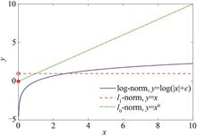
Hyperspectral Image (HSI) is composed of multiple discrete bands with specific frequencies. It not only contains rich spectral information but also provides real scenes that cannot be captured by human eyes, which is conducive to accurately target recognition. It has been widely used in earth remote sensing tasks such as compressed sensing, target classification, etc. However, limited by solar irradiance, optical imaging mechanism, and other factors, the equipment usually sacrifices part of the spatial resolution to ensure a high spectral resolution, which greatly limits the subsequent processing and application accuracy of spectral images. In contrast to HSI, Multispectral Image (MSI) obtained by multispectral sensor has high spatial resolution but low spectral resolution. To date, the fusion of High Spatial Resolution Multispectral Image (HR-MSI) and Low Spatial Resolution Hyperspectral Image (LR-HSI) in the same scene into High Spatial Resolution Hyperspectral Image (HR-HSI) is a common method to realize high-quality HSI reconstruction.In the early methods, multidimensional HSI data are often transformed into matrix processing. However, HSI is essentially a kind of 3D data with two spatial dimensions and one spectral dimension. Transforming multidimensional HSI data into matrix will inevitably destroy its spectral-spatial structural correlation and reduce the model performance.Tensor representation can effectively preserve the inherent structural information of spectral images. The method based on tensor decomposition has also become one of the effective schemes to solve the problem of HSI-MSI fusion. The methods based on tensor networks, such as Tensor Train (TT) decomposition and Tensor Ring (TR) decomposition, have stronger ability to mine the internal structure of data than other techniques. In addition, in recent years, some researchers have explored the potential properties of tensor ring factors. These methods have achieved satisfactory results, but with two problems remain. Firstly, these models expand the factors into mode-n matrix, ignoring the correlation between different modes; Secondly, the matrix nuclear norm constraint attempts to model the tensor in the vector space based on matrix Singular Value Decomposition (SVD), and its representation capacity will be lost. Tensor Nuclear Norm (TNN) based on t-SVD (tensor singular value decomposition) can effectively maintain the inherent low-rank structure of tensor and avoid the loss of original information in the process of tensor matricization. Besides, the larger singular value in the image usually corresponds to the more important information, such as contours, sharp edges and smooth regions. However, TNN treats each singular value equally, which means that the larger singular value will be punished greatly and will suffer from the loss of the more important information and lead to suboptimal solution in practical applications.Therefore, aiming at the problem of HSI-MSI fusion, a low-rank tensor ring decomposition based on nonconvex tensor rank constraint is proposed. Specifically, the intrinsic low-rank structure of hyperspectral images is mined by directly applying the nonconvex tensor nuclear norm constraint based on t-SVD. Firstly, HSI is projected into a low dimensional compact space by using the global spectral low-rank of the hyperspectral image. Then, following the spatial nonlocal similarity, the reduced image is divided into multiple patches, and the similar ones are gathered one by one to form several three-dimensional tensor groups. Furthermore, the tensor ring decomposition technique is used to mine its internal low-rank structure and explore the essential characteristics of tensor ring factors. Different from the way that expands the factors into matrices and applies the nuclear norm constraint, this paper proposes to directly apply the nonconvex tensor nuclear norm on each factor, which fully exploits the inherent tensor structure and effectively avoids the loss of spatial-spectral correlation. In addition, this paper introduces log-function instead of l1 norm to avoid excessive punishment of large singular values. Extensive experimental results show that the proposed method effectively improves the quality of the restored image. Compared with the latest fusion methods, the algorithm has better performance in quantitative evaluation and visual comparison.
Feb. 25, 2022Vol. 51 Issue 2 0210003 (2022)
Yan YANG, Jinlong ZHANG, and Xiaozhen LIANG
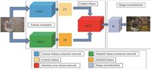
Haze scenes seriously affect the working performance and accuracy of computer vision systems. As an important research direction in the field of computer vision, image dehazing has always attracted the attention of researchers. Convolutional neural networks play a good role in image processing problems by virtue of their advantages. Therefore, convolutional neural networks are also used in image dehazing tasks. The mainstream dehazing algorithms are mainly divided into two categories, one is the image recovery algorithm based on atmospheric scattering model, and the other is the training learning dehazing algorithm based on convolutional neural network. Although the recovery class of dehazing algorithms considers the nature of haze image formation and obtains good results, the pathological nature of the atmospheric scattering model leads to the need for precise a prior conditions and harsh constraint rules, making the applicability of this class of algorithms limited. The idea of convolutional neural network-like dehazing algorithm is to train a convolutional network model with dehazing capability on synthetic dataset. In recent years, some researchers have designed a variety of image dehazing networks, although all of these networks achieve the effect of image dehazing, they still have many shortcomings. The main manifestation is that the dehaze image is too dark, the detail is lost seriously, the color is distorted and the dehazing is not complete. To address these problems, an image dehazing algorithm based on step-type network extraction and attention cross-fusion mechanism is proposed. The whole network model contains three modules, the stepped feature extraction network, the feature fusion module based on the attention mechanism and the clear image generation module. Among them, the step-type network performs detail and contour feature extraction of haze images, the fusion module adaptively fuses the detail and contour features in an attention mechanism, and the generation module outputs the dehaze images. In the feature fusion module, the residual structure is introduced to enhance the feature information and improve the accuracy of the network. The loss function used for network training is a combination of mean square error loss and perceptual loss, and the perceptual loss can effectively improve the semantic information of the features with haze images, which in turn leads to a more accurate dehaze image. The network model is considered to reach stability after the loss values reach convergence. After the network model is trained, rich experiments are used to demonstrate the validity and feasibility of the proposed model. The experiments in this article include two parts: the main experiment and the ablation experiment, and both the main experiment and the ablation experiment are analyzed in comparison from two perspectives: subjective evaluation and objective evaluation. The subjective evaluation uses experimental objects with haze images in real environments and synthetic images in datasets, and the objective evaluation uses some publicly available and widely used quantitative metrics. The experimental results show that the proposed model has good results for both haze images in real environment and synthetic images in the dataset. The dehaze image obtained by the proposed model has richer detail information, more natural color effect, more suitable brightness information and more complete dehazing effect. Experiments on different datasets demonstrate the wide applicability of the proposed model. In the objective evaluation, the proposed model also shows a clear advantage. It has a clear lead in the no-reference metric visible edge increase rate, average gradient, number of saturated pixel points and histogram similarity, and also outperforms the comparison algorithm in structural similarity and peak signal-to-noise ratio. The main experiments demonstrate the validity and feasibility of the proposed model, and in addition, local detail comparison experiments are used to demonstrate the performance of the proposed Moses on the detail information of the dehaze images. To demonstrate the necessity and importance of each component module in the proposed model, ablation experiment is used in this paper. The ablation experiments demonstrate the effectiveness of the step-type network for extracting detail features and contour features, and the effectiveness of the fusion approach under the attention mechanism. Although the proposed model obtains better dehazing effect, it is weaker for dense haze images. The dehazing method for dense haze images is something that needs to be focused on in the future.
Feb. 25, 2022Vol. 51 Issue 2 0210004 (2022)
Junxia WAN, Shanling LIN, Ting MEI, Zhixian LIN, and Tailiang GUO
Electrowetting display is a new reflective display which depends on ambient light display. It has the advantages of low power consumption, no radiation, fast response speed and easy colorization. It has a broad application prospect in electronic paper industry. However, in practical application, there are some problems in electrowetting electronic paper, such as ink reflux, oil film rupture, charge capture, contact angle hysteresis and so on. When electrowetting electronic paper displays images, there will be some problems, such as unclear image detail texture, image distortion and low contrast, which affect the display of electrowetting electronic paper. In view of the display characteristics and existing problems of the electrowetting display, in order to highlight the image of the target area more effectively and improve the contrast of the image, an image enhancement algorithm of electrowetting display based on image segmentation and dynamic histogram equalization is proposed. This algorithm combines the advantages of Otsu and maximum entropy segmentation algorithm, and proposes Otsu and maximum entropy threshold segmentation algorithm based on variance weight. Firstly, using this segmentation algorithm, the image is divided into background area and target area. Secondly, the original image histogram is divided into four sub histograms by taking the brightness mean value of the two regions and the selected threshold based on variance weight as the segmentation points, and then the sub histograms are reassigned. Finally, the four sub histograms are equalized. The advantage of this algorithm is to separate the target area and background area of the image and carry out targeted enhancement processing. While maintaining the average brightness of the target area and background area of the image, it improves the contrast of the image and highlights the target area of the image, so as to enrich the details of the image and make the whole image three-dimensional and full. The algorithm is simulated on MATLAB platform. Experimental results indicate that compared with other HE algorithms which partition the histogram, the image quality evaluation index PSNR is improved by 25.6%~45.5%, the entropy difference ΔE is reduced by 29.1%, and SSIM is closer to 1. At the same time, when it is applied to the electrowetting display, the image has higher contrast, the content of the image becomes richer and has better visual effect.
Feb. 25, 2022Vol. 51 Issue 2 0210005 (2022)
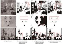
Huijuan TIAN, Jiahao ZHAI, Jianxin LIU, Jiawei LIU, and Linlin DENG
In recent years, iris recognition has been widely used in various fields. Iris segmentation is the most critical step in the iris recognition process. The accuracy of the iris segmentation algorithm directly affects the performance of the entire iris recognition system.In this study, an iris image segmentation algorithm SRN-UNet (SeResNext-UNet) is proposed to solve the problem of low segmentation accuracy for segmenting low-quality iris images. In the coding stage, the SE-ResNext module is added, which is cascaded with the SENet (Squeeze-and-Excitation Network) module after the RexNext module. The ResNext module can improve the network performance without increasing the network parameters; the SENet module builds a network model from the perspective of feature channel correlation through squeeze, excitation, and weight redistribution. For low-quality iris images, the SENet uses global information to selectively emphasize informative features and suppress less useful ones, and improve the accuracy of iris segmentation. In the up-sampling layer of the decoding stage, the amount of model parameters is reduced to increase the training speed. In order to solve the problem of image category imbalance, the SRN-UNet is trained by combining the Focal loss function and the Dice loss function. Among them, the Focal loss function can reduce the weight of easy-to-classify samples, make the model pay more attention to the training of difficult samples, and guide the network to retain complex boundary details; the Dice loss function can solve the problem of pixel category imbalance and alleviate the noise caused by the Focal loss function. Experimental results based on CASIA-Iris dataset and self-built low-quality iris image dataset show that compared with other algorithms, the proposed algorithm has better segmentation effects in terms of visual effects and objective evaluation indicators. Among them, the Mean Intersection Over Union of the proposed algorithm reached 95.19%, the F1 score reached 97.48%, and the Precision reached 97.82%. Compared with U-Net, the Mean Intersection Over Union, F1 score and Precision of proposed algorithm have increased by 4.20%, 2.27%, and 5.38% respectively, and the algorithm is faster than U-Net.
Feb. 25, 2022Vol. 51 Issue 2 0210006 (2022)

Tianwei YU, Enrang ZHENG, Junge SHEN, and Kai WANG
Remote sensing, a kind of detection technology, provides non-contact surface observation through sensor platform. With the rapid development of unmanned aerial vehicle, remote sensing and satellites technology, quantitative remote sensing images with higher resolution can be generated. Compared with medium and low-resolution remote sensing images, these high-resolution remote sensing images contain richer ground objects and spatial details, which can express the spatial structure and texture features of ground object more clearly, providing good conditions and foundation for remote sensing image interpretation and analysis. Therefore, high-resolution remote sensing images have become an important data source for fine earth observation. The scene classification of high-resolution remote sensing image refers to the analysis of extracted remote sensing image information, dividing the scene image of interest to different categories, such as forest, river, railway, etc., and is widely applied in environmental monitoring, urban planning, military object detection, global climate change research and other fields. Unlike general natural images, the geometry structure and space pattern of remote sensing images are highly complex, and there are also problems such as complex background and many types, which is a great challenge for effectively describing remote sensing image content. In addition, as a result of the complexity and diversity of remote sensing image scenes, different scenes may contain almost the same ground object targets, or the same scene may contain different ground object targets. At this regard, how to design discriminative feature representation to describe the image directly affects the quality of scene classification. In the past few decades, many approaches have been proposed, and most of these methods can be divided into two main categories. The traditional scene classification methods, such as Scale Invariant Feature Transform (SIFT), Histogram of Oriented Gradients (HOG) and Color Histogram (CH), mainly use hand-crafted feature but highly depend on the priori knowledge of the designer, resulting in the features with low-level semantics and limited representational capacity. By contrast, convolutional neural network has been successfully applied in remote sensing scene classification as its excellent feature self-learning ability. It can learn features directly from data without the need of priori knowledge of the designer. However, the accuracy of the scene classification approach based on CNN largely depends on the network structure and due to the complex spatial patterns, large inter-class similarity and high intra-class diversity of remote sensing scene images, the scene classification accuracy is severely limited. To address above issues, a novel remote sensing image scene classification algorithm via multilevel cross-layer bilinear fusion is proposed. Firstly, ResNet50 avoids the issues of model overfitting and gradient vanishing. It is employed to extract the remote sensing image multi-level features. In this way, the four multi-scale multi-level features of conv2_x, conv3_x, conv4_x and conv5_x layers were extracted by ResNet50 model. The dilated convolution with different expansion rates can perceive scene information at multiple spatial scales, promoting the network to acquire features at different scales. The context features at multiple spatial scales are extracted by setting the expansion rate of dilated convolution to different values. Then, the scene semantics of the feature information is enriched by serial fusion of multi-scale features. Since features at different levels contain different types of information, the high-level features provide global semantic information, which is helpful to identify and locate objects in the image. On the contrary, the low-level features contain rich local spatial information to refine and enrich the internal structure of salient objects. Such features can help high-level features to complement their loss of spatial information, which is beneficial for classification. The global context information of an image has a global receptive field. Considering the global information, the scene category can be inferred and the interference of background details can be filtered. By taking the advantages of low-level, high-level, and global context features, a multilevel attention feature fusion module is presented, which can effectively enhance the feature extraction capability of the model. The spatial attention is designed to focus on the key location of the scene image, which adaptively learn the importance of different image regions, depressing the irrelevant information of background. The global context information is integrated into the feature fusion process of low-level local features and high-level semantics features to realize the complementary feature information of each level, resulting in pleasing scene classification accuracy. Finally, inspired by fine-grained visual classification, a cross-layer bilinear fusion method is utilized to perform layered fusion of multilevel features, and the fused features are used for classification. Hadamard product operation at any two different levels is utilized to extract second-order bilinear information. Based on this cross-layer modeling to capture the association between local features, the hierarchical feature interaction and efficient information integration can be achieved, and the deep semantic information and shallow texture information contained in different hierarchical features are fully aggregated. Moreover, compared with the traditional bilinear pooling method, the Hadamard product is the product of two matrices′ corresponding elements, which does not change the dimension of the matrix, effectively solved the dimension explosion caused by the outer product operation. Through extensive experiments conducted on the UCM, AID and PatternNet datasets, the effectiveness of the proposed method is verified. Compared with other advanced approaches, the proposed method achieves more excellent classification performance. On the UCM dataset, for training with 80% data, the overall accuracy reached 99.32%, and the classification accuracy is increased by 0.75% compared with GBNet. On the AID dataset, the proposed method achieved 95.84% accuracy in 50% of training samples, with an improvement of 2.74% compared with ARCNet. On the PatternNet dataset, 50% of the samples are trained, and the overall accuracy is 99.6%, that has increased by 0.02% compared with SDAResNet.
Feb. 25, 2022Vol. 51 Issue 2 0210007 (2022)
Yanni WANG, Xuesong SUN, and Lixian YU
The marine environment is polluted and the marine ecological environment continues to be destroyed because of the over-exploitation and utilization of marine resources. Countries around the world have taken measures to solve the problem. In order to protect the coastal ecological environment, China has also begun to implement measures to monitor ships in the territorial sea and inshore waters. Ship detection is the focus of current research. Synthetic aperture radar has been widely used in the field of marine remote sensing monitoring because of its advantages such as all-time and all-weather monitoring, which provides strong data guarantee and technical support for multi-scale ship detection. With the improvement of the algorithm, researchers put more energy on the detection accuracy, while ignoring the detection speed and landing application of the algorithm. At present, the popular detection algorithms basically rely on the powerful graphics processing unit, so they can not be deployed in the front line of ocean monitoring. In order to solve the above problems, a lightweight SAR ship detection algorithm which can effectively enhance the receptive field is proposed in this paper. Firstly, ShuffleNetV2 is used as the backbone network. It is helpful to reduce the number of calculation parameters and memory consumption. Secondly, the improved space pyramid pool module is introduced. It not only expands the receptive field of the model effectively, but also makes the ship feature information be further mined. Simultaneously, the spatial attention module is added to enhance the model's attention to the spatial location information and improve the target positioning ability. Then, the improved path aggregation network is used to transfer more abundant ship positioning features from bottom to top. It is helpful to increase the shallow position information and multi-scale features. Finally, the experimental results on the SAR ship detection dataset show that the model size is 5.3 MB, the average detection accuracy is 94.7%, and the detection speed is 46 FPS. Compared with the current mainstream detection methods, it has fewer parameters, floating-point operations and smaller model size. It not only ensures high detection accuracy, but also realizes fast detection. The deployment verification is carried out based on the mobile phone. The results show that the ship can be accurately identified under the inshore complex background and offshore small target scene, the recognition accuracy is 85.7 %, and the test speed is 32 FPS. Compared with the computer equipment with excellent GPU performance, the detection accuracy and reasoning speed are all reduced, but still meet the real-time requirements. This method is helpful to transplant to FPGA or embedded mobile devices. It has great practical application value in real-time maritime safety monitoring and protection of marine ecological environment.
Feb. 25, 2022Vol. 51 Issue 2 0210008 (2022)
Junying ZENG, Yucong CHEN, Xihua LIN, Chuanbo QIN, Yinbo WANG, Jingming ZHU, Lianfang TIAN, Yikui ZHAI, and Junying GAN
Among biometric recognition technologies, finger vein recognition has attracted the attention of many researchers because of various advantages, such as noncontact collection, living body recognition, forgery difficulty, and low cost. The finger vein extraction is the key step of finger vein recognition technology, which directly affects the accuracy of the finger vein feature extraction, matching, and recognition.Most of the existing finger vein segmentation networks consume considerable memory and computing resources, and deploying them directly to the embedded platform is difficult. The design of lightweight deep neural network architecture is the key to solving this problem. However, most lightweight models have problems, such as sharp decline of segmentation performance, limited computing power, and real-time issue et al. To solve the above problems, this paper proposes an ultralight weight real-time segmentation network of finger vein textures-SGUnet. The SGUnet network realizes real-time finger vein texture extraction on an embedded platform, which is called finger vein segmentation. Moreover, there is a need to comprehensively consider the segmentation performance, network parameter size, and running time.First, the encoding-decoding structure is adopted in the overall network, and the hourglass shaped deep separable volume is used to actively reduce basic model parameters to realize the preliminary lightweight of the model. The lightweight and efficient attention module is used to realize the local cross-channel interaction without dimensionality reduction, improve network segmentation performance, and solve the problem of performance degradation during model compression. The attention module uses a one-dimensional convolution neural network to weight the channel in the operation process, while the introduced parameters of the attention module have little effect on the model’s burden. Second, most convolutional neural networks have a feature graph redundancy phenomenon. These redundant feature graphs have great similarities. They can be obtained from similar feature graphs through some simple changes. To solve the problem of partial feature graph redundancy, a swap operation is used to replace some “slack” convolution cores. A similar feature map is obtained through a simple mapping transformation, which ensures the consistency of network output, reduces the part of the convolution kernel, and realizes the second step lightweight of the model. Finally, to further reduce the number of parameters of the channel convolution and the problem that each group of information in group convolution cannot flow, the characteristic information of each group is randomly disrupted and reorganized using the method of characteristic information interaction to realize the information flow between group convolution, further compress the network, and ensure the performance of the model. After the above three steps of lightweight operation, an ultralightweight real-time segmentation network of finger vein textures is finally obtained.To verify the efficiency and real-time performance of this algorithm, two public finger vein databases are used: SDU-FV of Shandong University and MMCBNU-6000 of Quanbei National University of Korea. In the training process, four-fifths of the dataset is randomly selected as the training set and the remaining one-fifth as the test set. In the training and testing, the blocking strategy is adopted for the original image. Each image is divided into multiple patches. When the width and height are five steps, multiple continuous overlapping blocks are extracted from each image. The probability that the pixel is a vein is obtained by averaging the probability of all prediction blocks covering the pixel. To ensure that the memory limit and real-time performance of the hardware platform are not exceeded, selecting the patch with a step of five in terms of index and time is appropriate. After the network outputs the patch results, according to the order of sub patches, the overlapping sliding window strategy is adopted to retain the central region results, discard inaccurate image edges, and resplice them into a complete original image.In the experiment, SGUnet is compared with different segmentation networks, and the comparative experiment is conducted on the embedded platform. Compared with the traditional Unet segmentation network, the parameters of SGUnet model are approximately 1%, and MultAdds are approximately 0.5% of the traditional Unet segmentation network. We verify the network performance on two public finger vein datasets: SDU-FV and MMCBNU-6000. The results show that the segmentation performance of SGUnet network is not only better than that of large segmentation networks Unet, DU-Net, and R2U-net, but also surpasses the classic lightweight models squeeze-Unet, mobile-Unet, shuffle-Unet, and Ghost-Unet, Its performance indexes accuracy, dice and AUC reach 94.11%, 0.538 4, and 0.935 4, respectively. Compared with previous work, the proposed network has made great progress, in which the final parameter is only 145K and Flops is only 13M, and it surpasses previous lightweight models. Moreover, SGUnet network meets the low computing power requirements of the embedded platform and can be easily deployed on the whole series of NVIDIA embedded platforms to realize the real-time segmentation of finger vein veins. The test speed of finger vein veins extraction is as high as 0.27 seconds/piece.
Feb. 25, 2022Vol. 51 Issue 2 0210009 (2022)
Jianhui LI, Chunmei YANG, Caifeng ZHANG, Shen ZHANG, Xiaohong MA, Xiaojing WU, Tainye WANG, Xiuli YUE, and Minran CHANG
In the process of industrial production activities such as textile, printing and dyeing, coating and medicine, about 10%~15% of organic pollutants will be discharged into the surrounding water, soil and atmosphere with industrial wastewater, which increases the difficulty of organic dye treatment. Photocatalysis is considered to be one of the most promising technologies to solve the problems of energy shortage and environmental pollution in the future. It has been used to degrade organic pollutants. However, there are still many problems in the application of photocatalysts, such as low photon efficiency, high recombination rate of photoinduced electron hole pairs or poor stability. In order to expand the industrial application of photocatalytic technology, the modification of photocatalyst is an important direction to improve the utilization of solar energy. ZnO has the advantages of good photosensitivity, non toxicity, high electron mobility and low cost, but it is a wide band gap semiconductor, only responds to ultraviolet light, and the photon utilization is low. Bismuth oxyhalide BiOX (X=Cl, Br, I) has attracted extensive attention because of its special structure and excellent photocatalytic performance. As a typical bismuth halide oxide photocatalyst, BiOBr has a suitable band gap (2.61 eV), which makes it have the characteristics of good activity and stable photocatalytic performance under visible light irradiation. Therefore, it has become one of the materials that can not be ignored in the field of photocatalytic degradation of water pollution. However, the photocatalytic effect of pure BiOBr is poor. The combination of BiOBr and ZnO to form ZnO/BiOBr heterojunction can improve the photocatalytic activity of single component semiconductor photocatalytic materials and broaden the application range of ZnO and BiOBr. In previous studies, the binary composite ZnO/BiOBr was synthesized by hydrothermal method, and the dye degradation experiment was carried out to improve the photocatalytic degradation activity of single component. SHASHA Y et al. prepared ZnO/BiOBr complex by two-step hydrothermal method and showed excellent catalytic activity for the photodegradation of Methyl Orange (MO). GENG Y G et al. synthesized flower like ZnO/BiOBr by hydrothermal method, showing good photocatalytic degradation ability for Methyl Blue (MB). MENG X C et al. synthesized binary heterojunction ZnO/BiOBr by hydrothermal method. The photodegradation ability of Rhodamine B (RhB) was obviously better than that of single component. In previous studies, ZnO/BiOBr binary composites were synthesized by hydrothermal method, and some were synthesized by two-step method. This subject tried to synthesize ZnO/BiOBr with different morphology in one step by adding some ethylene glycol solvent. Although the photocatalytic activity could not be compared with previous studies due to different reaction conditions and degradation substrates, ZnO/BiOBr (1∶2) with high catalytic degradation activity was selected in this work. ZnO/BiOBr composite photocatalysts with different ratios of ZnO and BiOBr (1∶1, 1∶2, 1∶3, 2∶1, 2∶3, 3∶1 and 3∶2) were prepared. When the molar ratio of ZnO to BiOBr was 1∶2, the photocatalytic degradation performance of ZnO/BiOBr composite was the best. Under visible light for 120 min, the removal rate of Rhodamine B (RhB) (20 mg/L) was 98.89% and the degradation rate constant was 0.040 50 min-1, which was 4 times that of pure BiOBr. The binary composites ZnO/BiOBr were detected through X-ray diffraction, scanning electron microscopy, transmission electron microscopy, high resolution TEM, UV-vis diffuse reflection spectroscopy, photoluminescence analysis and electron spin resonance spectroscopy. X-ray diffraction analysis and transmission electron microscope analysis found that ZnO and BiOBr were successfully compounded. The scanning electron microscope analysis results showed that the the binary composite ZnO/BiOBr with different molar ratios showed flake structures of different sizes, and granular ZnO could not be seen on the surface of flake structures. Among them, the flake structure size of ZnO/BiOBr (1∶2) sample was the largest. UV-vis diffuse reflectance analysis showed that compared with pure ZnO, the band gap decreased significantly after BiOBr and ZnO were combined, indicating that the utilization range of spectrum was improved, which was beneficial to the improvement of photocatalytic performance. Photoluminescence analysis showed that the peak intensity of ZnO/BiOBr (1∶2) binary composite was between pure ZnO and BiOBr, indicating that the addition of BiOBr improved the utilization of photogenerated electrons and holes in pure ZnO. The results of reuse experiment showed that after repeatedly degrading Rhodamine B (RhB) 5 times, ZnO/BiOBr (1∶2) still maintained high activity, and the degradation rate of Rhodamine B decreased by 9%, indicating that the composite photocatalyst ZnO/BOBr (1∶2) had good stability. Electron spin resonance spectroscopy results showed that a large number of ·O2- and ·OH radicals were indeed produced in ZnO/BiOBr (1∶2) photocatalytic system. Therefore, it could be preliminarily concluded that ·O2- and ·OH radicals were important active species in ZnO/BiOBr (1∶2) photocatalytic reaction system. Combined with the theoretical analysis of semiconductor energy band, the existence of ·O2- and ·OH radicals was confirmed again, and the organics were degraded into small molecular substances through their oxidation. The photocatalytic degradation mechanism showed that the interface electric field was formed in the photocatalytic process of ZnO/BiOBr (1∶2) to inhibit the recombination of photogenerated electrons and holes. All results suggested that the ZnO/BiOBr (1∶2) composite with high photocatalytic degradation efficiency, excellent recyclability and stability can meet a potentially promising application for photocatalytic degradation of waste water.
Feb. 25, 2022Vol. 51 Issue 2 0216001 (2022)
Qingling MENG, Xianwei HU, Jiangyu YU, Zhongning SHI, and Zhaowen WANG
Surface Enhanced Raman Scattering (SERS) refers to the phenomenon that the Raman scattering signal of molecules adsorbed on some rough metal surfaces can be significantly enhanced. The combined effect of electromagnetic enhancement and chemical enhancement is widely recognized as the SERS mechanism by researchers. SERS substrates can be divided into simple SERS substrates and composite SERS substrates. Simple SERS substrates include metal electrode substrates, metal collosol substrates, and metal thin film substrates. Meanwhile, composite SERS substrates include bimetal composite substrates, oxide composite substrates, and flexible material composite substrates. Nono silver is a common-used metal SERS substrate.SERS is an important method to study the structure of the ionic liquid. The ionic liquid often works in a temperature range from room temperature to 100 ℃. However, there are few studies reported on the influence of temperature on the SERS effect. In the present study, firstly, silver SERS substrates are prepared by the constant-current electrodeposition method with current density of 0.5 A/dm2 at 35 ℃ for depositing 900 s. Then, the prepared silver substrates are roasted at 100 ℃ ~400 ℃, the influence of the roasting temperature on the morphology of the substrates is investigated, and the corresponding SERS mechanism is discussed. Finally, the prepared silver substrates are applied for the in-situ SERS spectra detection on 1-ethyl-3-methylimidazolium chloride (EMImCl) ionic liquid at different temperatures and the SERS effect is analyzed.The results show that in the substrate, the silver atoms form the dendrite consisting of a trunk and symmetric branches on both sides. The surface plasmon resonance generated by the dendrite gaps causes strong electromagnetic field, which can enhance the Raman signal of the adsorbed molecule. On the other hand, the branches have high curvature tips, which can produce lightning rod effect and improve the SERS performance of the substrates.In fact, the substrate is in an unstable metastable state, but the mobility of the silver atoms at room temperature is very weak. However, higher temperature can lead to stronger mobility of the silver atoms, causing the substrate transit to a more steady state with smaller free energy. Therefore, roasting process can make the nanoparticles reintegrate. As a result, the silver atoms in the high curvature part of dendrite can diffuse, causing the separation of grains. It is found that when the roasting temperature is 300 ℃, the tips of the branches begin to disappear and agglomerate. When the roasting temperature is raised to 400 ℃, the dendrites still exist, but the branches become thick and completely agglomerate, and it is noteworthy that very small spherical silver nanoparticles are formed on the surface of the dendrites.With R6G used as probe molecule, the SERS effect of the prepared silver substrates before and after roasting is investigated. It is found that the enhancement factor of the silver substrate decreases with the increase of roasting temperature. The enhancement factor of substrates before roasting is 1.62×10⁵. When the roasting temperature is 400 ℃, the enhancement factor reaches 2.16×10⁴, indicating that the SERS effect of the prepared silver substrates is still obvious. It is believed that changes of substrates′ structure reduce the “hot spot” area on the substrate after roasting. When the roasting temperature reaches 400 ℃, the newly generated spherical silver nanoparticles provide new “hot spot”, so that the substrates after high temperature calcination still have the SERS effect. However, the surface areas of the newly generated silver nanoparticles are very small, which greatly reduces the number of the adsorbed molecules, making the SERS effect weakened.The results of the in-situ Raman spectra detection on EMImCl with using the prepared SERS substrates show that the Raman spectrum signal is significantly enhanced. As the detection temperature increases from room temperature to 100 ℃, the ability of the substrate to enhance the Raman spectrum signal is not significantly weakened.
Feb. 25, 2022Vol. 51 Issue 2 0229001 (2022)
Chenglong ZHAO, Danfei HUANG, Zhiying LIU, Yuqi WANG, Aiqi ZHONG, Qinming ZHANG, and Fanhong MENG
The DFB laser with narrow linewidth and high side-mode suppression is used to develop a set of open TDLAS-WMS CO2 gas detection device. At present, most of the CO2 absorption spectra at 1 570 nm are still used. According to the query in HITRAN database, CO2 absorption intensity at 2 004 nm is stronger than that at 1 570 nm. The CO2 molecular absorption peak at 2 004 nm was selected as the absorption spectrum.Based on the detection principle of TDLAS technology, the Lorentz linear gas absorption spectrum was obtained through MATLAB simulation. Gas absorption spectrum wavelength modulation technique to obtain a second harmonic and harmonic signals, because even order harmonic signal strength down line center and the largest signal strength weakened along with the increase of harmonic times fast, odd harmonic signals in the spectrum of gas absorption peak amplitude getting minimum value is zero, so generally choose accidentally time, low harmonic detection of gas concentration, Odd harmonic is used to stabilize the frequency of the laser. In the experiment, the amplitude of the second harmonic signal after modulation and demodulation by a phase-locked amplifier is used to detect the gas concentration.The Herriott type gas absorption tank was designed based on the open environment because of the limitation of the widely used Herriott absorption tank to the detection method of microbial exhaled gas. Compared with the closed absorption cell, the open absorption cell reduces the detection time and operation complexity. The optical structure of absorption cell was simulated by using ZEMAX non-sequence mode. After ray tracing, the theoretical optical path could reach 1 350 mm, the actual optical path increased from 50 mm to 300 mm, and the lower limit value of detection concentration was reduced from 1 300 ppmv to 214.28 ppmv, which effectively improved the detection lower limit ability of the system.The experimental device uses STM32F103VET6 master controller, which controls the DDS chip AD9834 to generate high frequency sine wave signal and 12 bit D/A to generate low frequency sawtooth wave signal. The two signals are filtered and superimposed by the adder. The superimposed signals are converted into current signals to drive the DFB laser through the voltage controlled constant current source circuit. At the same time, the temperature control unit adjusts the temperature stability of the laser. The laser beam enters the open gas absorption cell, and the attenuated laser signal is detected by photodetector and collected by TLC2543 chip analog-to-digital conversion. After the signal is collected, it is sent back to the microcontroller for data processing. The processing results are stored in 32F205RGT6 chip and displayed on the upper computer.Through the configuration of CO2 gas detection of different concentrations, the amplitude of the second harmonic signal shows a good linear relationship with the concentration, and its fitting coefficient is 0.998 39. The concentration of the gas to be measured can be calculated by fitting the linear equation. CO2 gas at the concentration of 300 ppmv was continuously detected for 30 min, and the measured results ranged from 285 to 315 ppmv, indicating that the experimental device could continuously and stably detect CO2 gas. It proves that the second harmonic signal is reliable for concentration detection, and also verifies the stability of the detection device to a certain extent. Allan variance analysis was conducted within 300 s with CO2 of 300 ppmv. With the increase of integration time, Allan variance showed a trend of decreasing first, then stabilizing and then increasing. When the integration time reaches 101.6 s, Allan variance is in a stable state, and the sensitivity of the detection system is 1.512×10⁻⁵.The test results show that the detection device can accurately measure the concentration of CO2 gas. The detection device was used to study the concentration of CO2 gas produced by the respiration of Mycobacterium tuberculosis to provide a basis for the diagnosis of tuberculosis. In the field of microbial medical respiratory gas detection, rapid, accurate and stable detection is realized, and the system can be widely used in other open environment gas concentration measurement.
Feb. 25, 2022Vol. 51 Issue 2 0230001 (2022)
Bingxin TIAN, Jun HAN, Bingcai LIU, and Changmei GONG
Spectral imaging in biological tissue is an important detecting method in the biomedical field. Affected by the scattering effect of biological tissue itself, the scattered light passing through such tissues forms a group of chaotic speckles in the detector, which can not be imaged directly. Many methods have been proposed to focus and image through or in the scattering media. However, at present, it is still a challenge to realize non-invasive, non-wavefront-shaping spectral reconstruction in scattering media. Spectral intensity transmission matrix technology was first used to realize spectral retrieval from the speckle pattern through scattering media. This method requires an optical fiber spectrometer to obtain spectral information from speckle signals, although the spectral measurement system composed of multimode fiber has a high spectral resolution, its anti disturbance performance is poor, the spectral intensity transmission matrix of the fiber requires pre-calibrated, and it requires high stability of the mechanical structure. Spectral imaging can also be realized by matrix decomposition which requires a scanner to scan the pixels of the imaging surface to obtain the spectral data cube, and then compress and reconstruct it. However, the structure of the experimental system is complex. Moreover, both of these two methods can not analyze the spectra of different chemical substances through scattering media. Recently, the matrix transmission technology combined with the algorithm of the nonnegative matrix decomposition method has been proved to realize the 2D focus and imaging of fluorescent targets through the scattering medium. Although it is still unable to distinguish or retrieve the spectra of different chemicals in the scattering medium, in the case of multiple input modes, the detector receives multiple information of the target, which just provides sufficient data support for spectral analysis.Therefore, inspired by these two methods, we proposed a novel Nonnegative Matrix Factorization-based method, combined with the multiple input modes as the illumination to realize multispectral reconstruction of targets in biological tissue in a non-invasive way. This technique can be implemented in two steps. Firstly, the information of the hidden target is obtained by the optical method, and secondly, the spectra can be reconstructed by the computational method. In the first step, we utilize a phase-only SLM to modulate the laser source and generate multiple random input modes to illuminate the hidden targets behind the scattering media. Then an imaging spectrometer is employed to capture the spectral and spatial information of the hidden targets through a non-invasive detection optical structure. In this step, each input mode generates a spatial-spectral 3D image in the imaging spectrometer that can be compressed as a piece of mixed spectral information which can be resolved in the computational step. After achieving a series of mixed spectral information, that can be reshaped and stored into a 2D matrix in the second step. And the spectra information of the hidden object can be retrieved using the Nonnegative Matrix Factorization algorithm from the 2D matrix.The feasibility of this algorithm is verified by simulation experiments. We first test the samples with two spectral components and calculate the root mean square error and correlation coefficient between the reconstructed spectra and ideal spectra. Then, we carry out similar simulation experiments on samples with more spectral components and analyze the factors affecting the quality of spectral reconstruction from two aspects: the number of input modes and the similarity between two original spectra. The simulation results indicate that this method can quickly distinguish the multiple targets in the scattering medium and reconstruct the spectrum of each chemical of the targets simultaneously. And the reconstructed spectra have a high spectral correlation (greater than 0.99) and low root mean square error (less than 0.02) which means a reliable reconstruction. It also shows that more input modes and lower similarity among each original spectrum can improve the quality of spectral reconstruction. Finally, an example is given to illustrate the application of the proposed technique in scattering imaging. More than that, the method escapes the physical access to the tissue and is not only suitable for any kind of linear excitation signal but also provides a new way to resolve multiple spectra from the aliasing information. Moreover, it provides technical support for the resolution, focusing, and signal enhancement of multiple targets in the scattering medium.
Feb. 25, 2022Vol. 51 Issue 2 0230002 (2022)
Yu FAN, Huiqin WANG, Ke WANG, Zhan WANG, and Gang ZHEN
Spectral reflectance is considered as the “fingerprint information” of substances, which can reflect the essential properties of the color of substances. The true color of the substance under different light conditions can be accurately restored by obtaining the spectral reflectance information. It has important applications in printing, mural pigment recognition, textile and other scenes. Spectral reflectance reconstruction technology based on multispectral imaging has been widely used in recent years. It has the advantages of non-contact, high efficiency, diversified use scene and so on. The working process can be seen as using the low-dimensional multi-channel response signals output by various imaging devices to reconstruct the high-dimensional spectral reflectivity information of the object. Regression model method is widely used in spectral reconstruction because it has advantages in the model applicability of spectral reconstruction with small samples. The reconstruction accuracy in specific scenes has been continuously improved through the existing regression model reconstruction methods, but the optimization of model parameters in different reconstruction scenes has not been solved. The model is not adaptive enough to achieve the optimal effect of spectral reconstruction in multi-scene. To solve the problem of poor generalization performance of traditional regression model in spectral reconstruction of many scenes, multi-output least-square support vector regression spectral reflectance reconstruction method based on adaptive optimization in multi-scene is proposed to meet the application requirements of optimal spectral reconstruction model in multi-scene. Firstly, multi-output least square support vector regression is used as the reconstruction model, which simplifies the convex quadratic programming problem of traditional multi-output support vector regression. It improves the convergence speed of the model. Secondly, by combining the mean absolute percentage error and Pearson correlation coefficient, a comprehensive evaluation index of the model with adaptive weight is proposed, which can take into account the fitting accuracy and trend of the spectral reflectance reconstruction model. It is used as the fitness function of the sparrow search algorithm to optimize the parameters of the spectral reconstruction model, which can improve the generalization performance of the model. Simultaneously, Chebyshev chaotic map is introduced to initialize the sparrow search algorithm to prevent it from falling into local optimization in the process of optimization. Finally, the spectral reflectance of the test samples is reconstructed by using the reconstruction model with optimal parameters. To verify the effectiveness of this method, 213 standard RAL color cards are used as experimental data. Monochromatic CCD cameras and 10 narrowband filters are used as multispectral imaging systems. Compared with other traditional reconstruction methods, the average spectral root mean square error is reduced by 0.084 0, the average fitness coefficient is increased by 0.69%, and the average chromatic aberration is reduced by 1.23%. To verify the reconstruction effect of this method in different scenes, five different color regions on the temple murals and ancient painted cultural relics in a temple are selected for spectral reconstruction experiments. Compared with others, the average spectral root mean square error of this method is reduced by 0.029 2, the fitness coefficient is increased by 1.29%, and the color difference is reduced by 3.38%. The model parameters can be adaptively optimized for different reconstruction scenes, and better spectral reflectance reconstruction results are obtained in different reconstruction scenes. The experimental results show that this method can meet the requirements of high-precision color restoration of murals and painted cultural relics in practical application.
Feb. 25, 2022Vol. 51 Issue 2 0230003 (2022)
Gangcheng JIAO, Kaimin ZHANG, Yijun ZHANG, Xin GUO, Feng SHI, Hongchang CHENG, Lei YAN, and Jingjing ZHAN
In modern low-light-level night vision devices, the negative-electron-affinity GaAs photocathode, as the photosensitive core component, is usually prepared by alternating Cs/O activation on the cleaned GaAs surface. Meanwhile, the stability of GaAs photocathode is directly affected by the quality of Cs/O activation process and the residual gases in the vacuum environment. In order to improve the stability of GaAs photocathodes after activation and prolong the operating lifetime of the low-light-level night vision devices, experimental researches were executed from the perspectives of Cs/Oactivation method and decay characteristic with the aid of the self-developed ultra-high vacuum photocathode preparation and multi-information on-line measurement and control system. Two different Cs-O activation methods, namely the traditional 'yo-yo' method and the improved 'yo-yo' activation method were performed on the p-type GaAs (100) substrates grown by the vertical gradient freeze method. During the traditional 'yo-yo' activation process, the O source was introduced when the photocurrent dropped to 85% of the previous peak and the Cs source was kept continuously with a slight overdose, and then the O source was closed when the photocurrent reached a new peak. While in the process of the improved 'yo-yo' activation, the Cs source was maintained continuously and the O source was introduced when the photocurrent dropped to the minimum with the complete Cs overdose in the Cs/O alternate activation cycles, and the O source was also closed when the photocurrent reached a new peak. The Cs/O activation results show that the improved 'yo-yo' activation method with less alternate activation cycles can obtain a higher photocurrent peak and a higher spectral sensitivity than the traditional one with more alternate activation cycles. In addition, the photocurrent decay results under the long-time illumination of 633 nm demonstrate that the GaAs photocathode with the improved 'yo-yo' activation method can achieve a longer operating lifetime and a better stability than the traditional one. After 18 hours of decay under continuous illumination, the GaAs cathode sample using the improved 'yo-yo' activation method exhibited a smaller drop of spectral sensitivity, especially in the near-infrared waveband. obvious. At 800 nm, the sensitivity of the cathode sample using the improved 'yo-yo' activation method is decreased by 37%, while that of the cathode sample using the traditional one is decreased by 63%. Furthermore, by measuring the changes of components and partial pressure of residual gases in the activation chamber with the quadrupole mass spectrometry, and through fitting the photocurrent decay data based on the decay model related to the vacuum pressure and the partial pressure of residual gases, the weight factors of influence of different residual gases on the decay of photocathode performance were obtained. The fitting results show that the water vapor and carbon dioxide have the greatest impact, followed by methane and carbon monoxide, while hydrogen has almost no impact, and other hydrocarbon organic molecules also have the negative impact. By comparison of weight factors of residual gas components, it is found that the improved 'yo-yo' activation method has better immunity to the degradation of GaAs photocathode performance caused by the adsorption of residual gas molecules in the vacuum chamber than the traditional one. In order to verify the improvement effect of the improved 'yo-yo' activation method on the immunity of oxygen molecules, the photocurrent decay cases of GaAs photocathode samples activated by the two different activation methods, were tested under the illumination of 633 nm red light by introducing oxygen with different partial pressures into the activation chamber. The results show that the decay rate of photocurrent increases with the increase of oxygen partial pressure. Whereas, the photocurrent decay rate of GaAs photocathode sample with the improved 'yo-yo' activation method is significantly lower than that of GaAs photocathode sample with the traditional 'yo-yo' activation method. When the partial pressure of oxygen is 6×10⁻¹⁰ Pa, the photocurrent decay rate of the improved 'yo-yo' activation method is reduced by 75% compared with that of the traditional one, and when the oxygen partial pressure is 1.2×10⁻⁹ Pa, the photocurrent decay rate of the improved 'yo-yo' activation method is reduced by 54% compared with that of the traditional one. In general, the improved 'yo-yo' activation method can obviously delay the performance degradation rate of GaAs photocathode caused by the adsorption of oxygen-containing gas molecules on the surface, which will help to improve the stability of GaAs photocathode in low-light-level night vision devices.
Feb. 25, 2022Vol. 51 Issue 2 0212001 (2022)
Minge GAO, He YUAN, Min XU, Junhua WANG, and Hailong CUI
Opaque aspherical shells are widely used in the fields of aerospace, military and communications. The thickness measurement is a key issue to ensure the manufacturing quality of such components. Since it is impossible to conduct micron-level non-destructive measurement of the thickness directly, the flipping measuring method is preferred to measure the inner and outer contours of the shell. The thickness is obtained indirectly through the inner and outer contours. In the flipping measuring method, the centering accuracy before and after the reversal should be guaranteed, which is of significance for specifying the relative positions between the double surfaces. Most of the existing centering measurement technologies are limited by accuracy or complicated structures. Focusing on these limitations, a non-contact centering measurement technology based on laser interference is proposed. The optical structure only consists of two sets of the same laser interference centering device while the measurement accuracy can reach sub-micron level. The specific implementation process is to independently design and set up a bidirectional laser interference centering device and assist the modern photoelectric detection technology and a real-time feature extraction algorithm for laser interference fringes. Finally, the high-precision centering measurement before and after the reversal is achieved. In conjunction with the high-precision hollow air bearing table and a centering and leveling device, a bidirectional laser interference centering device is designed and built to collect the interferograms of the inner and outer surface before and after the reversal. Two sets of the same laser interference centering device are performed up and down to realize the bidirectional centering measurement of the tested part, which can monitor the consistency and tilt of the tested part before and after the reversal. The laser interference centering device adopts the Kepler telescope system to realize the expansion and collimation of the laser beam. The edge stray light is filtered by the pinhole to uniform light intensity. The core of the laser interference centering device is a dedicated lens group containing a reference sphere. This lens group compensates the aberration so that the reference light and the measurement light return back along the same path. The interferograms formed by the reference light and the measurement light are recorded by the detector. Based on the modern photoelectric detection technology, a real-time feature extraction algorithm is proposed to analyze the dynamic characteristics of the interference fringes with different motion postures, which greatly improves the accuracy of dynamic recognition of laser interference fringes. Specifically, the feature extraction algorithm includes filtering, removing background noise, image binarization, image morphology operations such as erosion, closing, opening, and ossification to sharpen the interference fringes, and the centroids extraction of multiple sets of interferograms. The least squares method is used to fit centroids to obtain the least squares radius, which is considered as the radius of rotation of the interferograms. The mathematical model has been built, in which the radius of rotation of the interferogram is treated as the input and the centering deviation of the evolving axis of the opaque aspheric shell and the rotation axis of the hollow air bearing table as the output. Once the radius of rotation of the interferogram is known,the definite centering deviation of the evolving axis of the opaque aspheric shell and the rotation axis of the hollow air bearing table can be calculated through the mathematical model built. The centering accuracy of the proposed technology is derived theoretically and compared with an inductance micrometer with a certain accuracy in the experiment. The experimental results are consistent with the theoretical results, which proves that the laser interference centering device and real-time feature extraction algorithm can effectively improve the centering accuracy. The absolute centering accuracy can achieve 0.424 microns. The centering measurement is carried out during the thickness measurement of the opaque aspheric shell by the flipping measuring method. Using the laser interference centering device and feature extraction algorithm proposed in this paper, the centering deviations of the evolving axis of the opaque aspheric shell and the rotation axis of the hollow air bearing table before and after the reversal are successfully specified. The centering measurement technology meets the centering requirements and provides a positioning guarantee for the thickness measurement accuracy of the opaque aspheric shell by the flipping measuring method. As a result, the accuracy of profile and thickness measurement of the opaque aspheric shell is improved.
Feb. 25, 2022Vol. 51 Issue 2 0212002 (2022)
Bin REN, Jianyuan CUI, Gang LI, and Haili SONG
Auto-driving is developing rapidly nowadays. Tesla, Nio and other car manufacturers have put their level 2 autonomous driving products on the market. As a kind of important sensors in the car, lidar can directly get the distance and angle to the object. That information is organized into the form called “point cloud”. Point cloud is mainly used to rebuild the 3D scene, which plays a major role in guiding the vehicle. But due to weather and other reasons, there is a large number of noise points in the point cloud data detected by lidar, which will cause the accuracy of 3D reconstruction to decrease, and the structure of the object cannot be fully reproduced. It is dangerous while driving since the vehicle does not have enough information about its environment. So, point cloud denoising is necessary and important.To solve this problem, this paper proposes a three-dimensional point cloud denoising method based on adaptive threshold, which has two stages. According to the Euclidean distance between noise points and non-noise points, this method divides the noise points into two types: far-signal noise points and near-signal noise points. For removing the two types of noise points, threshold adaptive denoising algorithm based on nonlinear function and denoising algorithm based on curvature are used respectively at different stages. At the first stage, the threshold adaptive denoising algorithm based on nonlinear function is to remove the far-signal noise. It uses ordered grids to organize disordered point clouds and calculates the average density of point clouds in the grid. Then, the nonlinear function whose input is the distance from the grid to the lidar is called for calculating the threshold to realize the adaptive adjustment of the denoising density threshold. The points in the grid whose density does not reach its threshold would be seen as noise points. At the second stage, the denoising algorithm based on the median is to remove the near-signal noise. It uses the K-D trees to organize the remaining point cloud data. Then all points in the neighborhood of a point P are sorted by curvature. Finally, the median curvature is calculated, and the point P greater than the median curvature is treated as noise points.To verify the proposed method, a set of experiments was carried out with the dataset from the Stanford 3D scanning repository. The origin data from the Stanford 3D scanning repository was seen as non-noise point clouds. And noise points were added whose amount is about 10% of the original data volume. The experiments showed that this method could effectively remove the noise points in the point cloud, and the denoising accuracy is above 95%.
Feb. 25, 2022Vol. 51 Issue 2 0212003 (2022)
Jianwei ZHANG, Yongqiang NING, Xing ZHANG, Yinli ZHOU, Chao CHEN, Hao WU, Li QIN, and Lijun WANG
The Vertical Cavity Surface Emitting Semiconductor Laser (VCSEL) has the unique advantages of circular symmetricalspot morphology, two-dimensional integration, narrow spectral width and small size et al. In particular, the wavelength of VCSEL laser is hardly changed with temperatures (0.06 nm/℃), also the output window of VCSEL has no Catastrophic Optical Mirror Damage(COMD), and thus the VCSEL can behave excellent performance in the high temperature environment with strict working temperature requirements. This paper mainly introduces the structure and operation principle of VCSEL, and the temperature stability characteristics of laser cavity mode and gain is analyzed when the VCSEL works at high temperatures. The alkali metal atomused in the precisequantum measurement can be pumped by high-temperature operating VCSELs. And the development of VCSELs for this application is introduced and reviewed. By adjusting the position of gain spectrum and the cavity mode of oscillation cavity, the increase of power consumption of VCSEL at high temperatures can be effectively suppressed. Through the integrated surface mode filter, the stable selection of the internal mode of VCSEL can be realized. The internal mode and polarization of VCSEL laser can be controlled at the same time by using the surface grating structure. The above reports have realized good performance of VCSEL at high temperatures. In the future, using nanostructure or external cavity to compress the linewidth level of VCSEL laser will be an important research field.The demand for high-temperature and high-speed VCSEL laser is also reviewed. And this VCSEL is mainly used in the datacenter, which is the basic for the 4G and 5G communications. As the huge energy consumption in datacenter becomes a serious problem. High-temperature operating VCSELs may relieve this problem. High-temperature and high-speed performance are the main research directions of VCSELs used in the datacenter. Based on the commonVCSEL structure, the working temperature of high-speed VCSEL can be increased to 150 ℃ by using conventional quantum well. The operating temperature of high-speed VCSEL can even be increased to 180 ℃ by using quantum dot active regions. VCSEL lasers with higher rate at high temperature need to make a breakthrough in the structure of quantum dot materials. In addition, using surface nanostructure instead of the existing DBR can effectively reduce the resistance of the traditional VCSEL, and further improve the modulation rate of VCSEL at high temperatures.
Feb. 25, 2022Vol. 51 Issue 2 0251201 (2022)
Ting WANG, Jiliang WU, Chunguang MA, Yongtao HUANG, Yuede YANG, Jinlong XIAO, and Yongzhen HUANG
In recent years, dual-wavelength lasers are used in a wide variety of applications in interferometric measurement, optical communications, microwave and THz wave generations, and optical frequency combs. A variety of methods to realize dual-wavelength lasers have been proposed, including fiber lasers, Y-branch integrated lasers, and two-section Distributed Feedback (DFB) or Distributed Bragg Reflection (DBR) lasers. In addition, the whispering gallery mode microcavity laser has great application potential in photonic integration due to its small mode volume, high-quality factor, and simple manufacturing process.In this paper, we design and fabricate a square microcavity laser with a current injection window in the center and four corners to achieve tunable dual-wavelength lasing. By simply changing the injection current, we realize dual-mode lasing with a wavelength interval tuned from 0.18 nm to 0.1 nm, and an intensity ratio less than 4 dB.A two-dimensional finite-element method is used to simulate the TE modes of the square microcavity. It can be seen that along the lines connecting the midpoints of the adjacent sides, the fundamental mode and the first-order mode show the strong field and the weak field distribution, respectively. Due to the incomplete overlap of the mode field distributions, there is less mode competition between the fundamental mode and the first-order mode, and the quality factors are 6.994×10⁴ and 1.838×10⁴, respectively. Taking into account the vertical radiation, material absorption, and manufacturing process losses, the two modes have similar quality factors to achieve dual-mode lasing.Based on the mode field distribution, a deformed square microcavity laser is designed with a current injection window in the center and four corners, which induces a refractive index step. For a square microcavity with a side length of 30 μm, the numerical result shows that the mode wavelength interval can be reduced from 1.07 nm to 0.11 nm when the refractive index step increases from -0.005 to 0.003.Next, a dual-mode square microcavity laser with a current injection window in the center and four corners is successfully fabricated with a side length of 30 μm, and a waveguide of 3 μm. The maximum output power coupled into a multimode fiber is 1.04 mW when the injection current is 77 mA. The series resistance is 11.4 Ω, and the threshold current is about 9 mA. When the injection current is increased from 41 mA to 53 mA, the wavelength interval of the microcavity laser decreases from 0.18 nm to 0.1 nm. Meanwhile, the intensity ratio is less than 4 dB. Since the lasing wavelength of InP-based lasers changes with temperature at a rate of 0.1 nm/K, the temperature difference between the injection window and the non-injection window can be estimated to be 2.5 K when the injection current is 50 mA. Compared with the simulation results, the refractive index step corresponding to the dual-mode interval of the microcavity laser increases from 1×10⁻³ to 3×10⁻³ with the increase of the injection current. It indicates that the refractive index of the microcavity laser is mainly affected by the temperature distribution. According to the experimental and simulation results, the refractive index step and the current have a quadratic relationship. In addition, a period-one oscillation phenomenon appears due to the further reduction of the dual-mode interval.For comparison, a square microcavity laser with a square-ring-patterned contact window is also fabricated with a side length of 26 μm, and a waveguide of 2.5 μm. The dual-mode interval gradually increases with the increase of the injection current. When the injection current is increased from 62 mA to 85 mA, the dual-mode interval can be tuned from 0.202 nm to 0.284 nm. It further verifies the conclusion that the refractive index is mainly affected by the temperature distribution.In conclusion, a square microcavity laser with a non-uniform injection window in the center and four corners is designed to realize dual-mode lasing with tunable intervals. When the injection current is increased from 42 mA to 53 mA, the wavelength interval decreases from 0.18 nm to 0.1 nm. The proposed square microcavity laser with a current injection window in the center and four corners provides a light source with a tunable interval for the generation of microwaves, optical frequency combs, and the potential chaotic lasers.
Feb. 25, 2022Vol. 51 Issue 2 0251202 (2022)
Yukun WANG, Zhongming ZHENG, Hao LONG, Yang MEI, and Baoping ZHANG
There are many kinds of semiconductor lasers, such as Distributed Feedback Laser Diode (DFB-LD), Edge Emitting Laser (EEL) and Vertical Cavity Surface Emitting Laser (VCSEL). Among them, VCSEL has many advantages such as large-scale two-dimensional integration, circular far-field spot, single longitudinal mode output, low power consumption, on-wafer testing, low threshold, small divergence angle, high modulation rate and so on. Hence, VCSEL has attracted the attention of many researchers.VCSEL has a history for more than 40 years. It was proposed firstly by Kenichi Iga of the University of Tokyo in 1977. After more than 40 years of research by scientists, applications and development of GaN-based VCSELs have been in the fast lane, including lighting, communication, projection display, optical storage, medical treatment, micro atomic clock and sensor.Nitride is an ideal material for manufacturing optoelectronic devices in ultraviolet to near infrared. Wherein, Aluminum Gallium Nitride (AlGaN) is one of the important materials for nitride semiconductors. Its bandgap is continuously adjustable from 3.4 (GaN) to 6.2 eV (AlN), corresponding 365 to 200 nm. It is an ideal material for fabricating ultraviolet VCSEL from near ultraviolet to deep ultraviolet. After nearly 20 years of rapid development, AlGaN-based VCSELs have become the research hotspots of semiconductor lasers.Recently, violet to yellow green VCSELs have been demonstrated with electrical pumping, while there are only a few reports about ultraviolet (UV) VCSELs with optically pumping. Comparing with the visible nitride VCSELs, the development of UV VCSELs faces many challenges, especially in deep ultraviolet (DUV) range (< 280 nm), including obtaining high crystalline quality AlGaN epilayer, DBR fabrication, sapphire substrate removal, reducing surface roughness, current spreading structure, high carrier injection efficiency, high doping level of p-AlGaN, and ohmic contact with p-AlGaN layer. Firstly, AlGaN epilayer with higher Al component is desired. However, with the increase of Al composition, the growth of AlGaN epilayer become more difficult, because of high growth temperature, and low surface migration speed of Al element. Secondly, it is difficult to prepare high-quality nitride DBR with high reflectivity in UV range, which is results from the lattice mismatch, thermal expansion coefficient mismatch, uneven in-plane components and small refractive index difference. Thirdly, dielectric DBR is easy to fabricate, however, it requires substrate removal, which is hard to realize. It also absorbs light in DUV. For electrically pumped AlGaN-based VCSELs, the fabrication is more complex and difficult than that of optically pumped, and more challenges need to be overcome. Firstly, high p doping level AlGaN is difficult to obtain, because Mg element is hard to dissolve in AlGaN material, and the activation energy increases with Al component (~200 meV in GaN, ~630 meV in AlN). As a consequence, the conductivity of p-AlGaN is low. Secondly, the current spreading structure is required to provide sufficient and stable carriers into the active region, so as to achieve population inversion, and form a continuous output laser. The current spreading layer in VCSEL should be of high conductivity and low optical absorption, which is obstructed by the p doing problem. Thirdly, carrier injection efficiency is often reduced by electron overflowing from active region and low hole injection into active region. For short wavelength VCSELs, especially in DUV, electron leakage is more serious, and hole concentration in p-AlGaN is much lower. Therefore, reasonable design of Electron Barrier Layer (EBL) should be considered, and increasing p doping level is desired.Although there are many technical difficulties, the prospect of AlGaN-based UV VCSEL is still full of opportunities. As the ultraviolet devices, especially in DUV, have great demand in many applications, such as medical diagnosis, biochemical medicine and prevention, atomic capture, spectroscopy, laser lithography, laser high density storage and other important fields, it will be a key component essential to supporting the information society in the future.In this paper, the history of GaN-based VCSELs was reviewed, and its main applications were briefly introduced. Then, the research progress of blue, green and ultraviolet VCSELs was also introduced. Finally, the challenges and difficulties in the development of optically pumped and electrically pumped ultraviolet VCSELs were analyzed, and the improvement and optimization methods were briefly introduced.
Feb. 25, 2022Vol. 51 Issue 2 0251203 (2022)
Lilong MA, Minchao XIE, Wei OU, Yang MEI, and Baoping ZHANG
Semiconductor microcavities can restrict photons in a small volume compared to the wavelength of light, and can artificially adjust the spontaneous emission characteristics of the active medium in the cavity, which is important for the development of more efficient optoelectronic devices. At the same time, semiconductor microcavities also provide a good platform for the fundamental research of cavity quantum electrodynamics. Optoelectronic devices based on semiconductor microcavity have been widely used, such as microcavity lasers, microcavity sensors, microcavity optical filters, etc. Optical microcavities are usually divided into three types: Fabry-Pérot (FP) microcavities, Photonic Crystal (PC) microcavities, and Whispering-gallery Mode (WGM) microcavities. In WGM semiconductor microcavities, photons circulate along the sidewall of the waveguide layer, and the optical field is confined by total reflection at the interface between the waveguide layer and the surrounding air. Therefore, WGM microcavities can achieve high quality (Q) value and small mode volume. Compared with the FP and PC microcavities, WGM microcavities have the advantages of simple structure, convenient preparation, and easy integration with large scale optoelectronic circuits. GaN based semiconductor materials are featured with direct wide bandgap, including aluminum nitride, gallium nitride, indium nitride, and a variety of alloys between them. By adjusting the composition of the alloy, the emission wavelength can cover from deep ultraviolet to the near-infrared band. They are very important for the preparation of optoelectronic devices. In addition, GaN based semiconductor materials with high exciton binding energy and oscillator strength can be combined with WGM microcavity to achieve micro-cavity optoelectronic devices with small size and high efficient, which can be used for cavity quantum electrodynamics studies at room temperature. Therefore, GaN-based WGM microcavity light-emitting devices have attracted the attention of many researchers, and have been widely used in optoelectronic integration, spectral analysis, and other fields.To date, there have been many reports about GaN microdisk based lasers and sensors on Si, and laser emission wavelengths have covered from UVC to the green spectral range. However, GaN based microdisk cavities on Si are also faced with many difficulties, including the lattice constant mismatch and thermal expansion coefficient mismatch between GaN and Si substrates, and the melt etching during epitaxial growth, etc. There is a 17% lattice mismatch between GaN and silicon, usually resulting in a high threading dislocation density (typically 1 010 cm-2) during epitaxial growth. This can reduce the internal quantum efficiency of the active region, and cause the interface roughness of the GaN film, thus increasing the scattering loss of the microcavity. On the other hand, the thermal expansion coefficient mismatch between GaN and Si substrate is as large as 54%, which leads to large tensile stress in GaN film during the cooling process after epitaxial growth, resulting in wafer warping and even cracking. Therefore, to ensure the quality of the active region, it is usually necessary to grow thick stress adjustment and defect filtration layers. Moreover, the Ga source used in epitaxial growth can corrode Si substrate, that is, melt etching. A certain thickness of AlN buffer layer is usually grown to protect Si substrate before GaN growth. As a result, the total thickness of GaN epitaxial layer on Si substrate is large (generally >1 μm). The large thickness of microdisk makes it difficult to guarantee the single-mode operation, and can reduce the light confinement ability and microcavity effect. In addition, the nitrides near the substrate often have high density defects and dislocations, and their internal optical absorption and scattering losses can be large. This can also affect the Q factor and the threshold of the microdisk laser.To solve the above problems, a new method of device preparation is proposed in this study. Devices fabricated by this method avoid the influence of poor crystal quality and large thickness of GaN layers directly grown on Si substrate. Sapphire substrate is used for the GaN growth in this study to ensure crystal quality. During the fabrication of microdisks, the epitaxial layer was transferred to the Si substrate, and the rich defect layer close to the substrate during the original growth was removed. After that, a simple SiO2 sacrificial layer wet etching technique was used to realize the air gap structure between GaN microdisk and Si. High Q GaN microdisk cavity on Si with low lasing threshold was successfully realized under the condition of optical pumping. The cavity Q factor is up to 10 487. The device threshold energy is as low as 5.2 nJ/pulse, corresponding to an energy density of 33.6 μJ/cm2. Owing to the good crystal quality and low cavity losses, the device can still maintain excellent laser characteristics at 100 ℃. The device preparation method in this study also has good flexibility, and the GaN-based microdisk resonator can be fabricated on different kinds of substrates, such as metal, polymer, quartz, etc.
Feb. 25, 2022Vol. 51 Issue 2 0251204 (2022)
Jiachen LIU, Yongzhen HUANG, Youzeng HAO, Ke YANG, Yuede YANG, and Jinlong XIAO
In this paper, by establishing a tri-mode rate equation model with a gain spectrum model and Langevin noise sources, the relative intensity noise, frequency noise and linewidths of a WGM microcavity laser are investigated numerically, and the influence of the mode competition on noise characteristics of the microcavity lasers is mainly studied.The steady-state characteristics of the microcavity laser are simulated by the tri-mode rate equation model including carrier densities, photon densities and mode phases. The mode skipping due to the thermal effect caused by the injection current is simulated. As the temperature increases due to the current injection, the lasing wavelength of the microcavity laser redshifts and the mode skips with the increase of the injection current. The effect on the optical power, relative intensity noise, frequency noise and linewidths are studied by inducing Langevin noise sources to the rate equations. When the microcavity laser is at a single-mode lasing state, the relaxation oscillation peaks of the relative intensity noise and frequency noise spectra both move to the high frequency with the increase of the injection current, and the whole relative intensity noise and frequency noise decrease. Relative intensity noise refers to the ensemble average of the fluctuations of the laser power relative to the average power squared. The relative intensity noise approaches the standard quantum limit of -165.5 dB/Hz at a high bias current of 115 mA, a long integral time of 50 μs and a short time step of 1 ps. The frequency noise of the laser refers to the random fluctuation of instantaneous mode frequency, which comes from the natural phase noise of the laser caused by the spontaneous emission, and phase noise caused by carrier fluctuation. And the linewidth of the microcavity laser, which is the full-width at half-maximum of the single-mode spectrum, is determined from the low-frequency of the frequency noise spectrum. By averaging the frequency noise at the low-frequency of the frequency noise spectrum, a low linewidth of 85.6 kHz for the microcavity laser could be obtained with I=115 mA and Q=2.5×10⁴, which is smaller than the measured laser linewidth.Furthermore, the fast Fourier transform is proposed to simulate the laser spectrum using the mode electric field expressed by the mode photon density and the mode phase. When the injection current is 115 mA and the integral time is 50 μs, the optical spectrum of the laser line shape is obtained and the simulated linewidth of the microcavity laser by Lorentz fitting is 77.2 kHz, which is about 10% smaller than that obtained from the frequency noise spectrum.When the microcavity laser is dual-mode lasing, the relative intensity noise and the frequency noise of each mode increases obviously at the low-frequency due to the mode competition. When the injection current is 51 mA, the microcavity laser is dual-mode lasing at modes M1 and M2. The relative intensity noise at low-frequency increases by 25 dB/Hz, and the linewidths of the two modes with output powers of 3.33 mW and 1.63 mW, calculated from the frequency noise spectrum at low frequency, are 1.5 times and 6 times of the linewidth at single-mode lasing state with the same output power. The linewidths of the dual-mode lasing state are significantly widened, which is consistent with the experimental results. The mode electric field is also analyzed with the help of the fast Fourier transform and the laser linewidths obtained from the lasing mode spectra are in agreement with those obtained from the frequency noise spectra. The dynamic change process of the frequency noise and the linewidth at dual-mode lasing state are studied when the injection current varies from 50 to 52 mA. When the side-mode suppression ratio is less than 20 dB, the laser linewidth begins to widen. The frequency noise at low-frequency of the high power state mode rises faster than that at high-frequency, and the frequency noise at low-frequency of the low power mode falls slower than that at high-frequency, which makes the frequency noise at low-frequency of the microcavity laser always in a high state and widens the linewidth of the microcavity laser .
Feb. 25, 2022Vol. 51 Issue 2 0251205 (2022)
Jiankun WANG, Yongguang HUANG, and Yihui LIU
Semiconductor laser is one of the core light sources of optical fiber communication systems. Better semiconductor laser performance helps to increase the capacity and quality of the entire fiber optic communication system. In order to design better semiconductor lasers, it is often necessary to simulate various performances through rate equations. However, some parameters need to be obtained through experimental results, so it is necessary to fabricate semiconductor laser chip to extract the parameters. Through multiple rounds of iterative experiments and theoretical calculation, chip optimization is continuously carried out to achieve the final goal. In the process of optimization analysis, in order to better analyze the performance of laser chips, laser parameters are usually divided into eigen parameters and parasitic parameters. Parasitic parameters mainly include capacitance, resistance and other properties. They can be obtained by means of a fitting method by combining a reflection curve of the small-signal frequency response (S11) with an equivalent circuit model. These parameters are basically not affected by the laser-current change. However, the extraction of the eigenmetric parameters is related to the selected laser-current range, and the parameter extraction results themselves have a variety of possible answers. How to obtain more accurate and suitable for a wide operating current range of eigen parameters is the focus of this paper. In recent years, with the development of emerging applications such as 5G optical communication and Radio On Fiber (ROF) analog communication, semiconductor lasers are required to operate at larger drive currents to improve high-speed performance and are required to have better linearity. In such ROF analog communication systems, semiconductor lasers need to work at a lager bias laser-current and in the linear region to obtain excellent microwave performance. Besides, it is need to test and evaluate many microwave performance indicators, such as third-order intermodulation, second harmonic, relative intensity noise, etc. The acquisition of these indicators requires complex test systems, expensive equipment and difficult testing. Therefore, how to accurately and conveniently obtain the microwave performance of the laser at a large drive current is particularly important. By testing some basic performance of the laser, the eigenvalue and parasitic parameters of the semiconductor laser can be extracted. These extracted parameters, combined with system characteristics, can be used to quickly calculate and evaluate most of the microwave performance of the system. This method greatly reduces the test requirements and the costs of test equipment, greatly speeding up the performance evaluation of semiconductor lasers and the entire design process. The traditional parameter extraction method can obtain the parameter values of semiconductor lasers operating at low bias currents (10~40 mA). But the parameter extraction at large currents is not very accurate, and more complicated tests such as measuring chirps are required. This paper re-evaluates the applicability of approximate conditions in common semiconductor laser parameter extraction methods and finds that approximate conditions fail at large currents. To this end, it is proposed to use a more general formula for the parameter extraction of the semiconductor laser rate equation. Taking the DFB laser chip as an example, the small-signal frequency response curve (S21) is used to accurately extract the resonant frequency fr and the damping factor γ of the semiconductor laser, and combined with the laser power-current (P-I) response curve of the laser, the various parameters of the semiconductor laser rate equation can be calculated. Compared with the previous parameter extraction approximation calculation method, the present method has three advantages. First, the range of laser drive currents that can be analyzed is wider. Second, there are fewer items to test. The third is that the extraction of parameters such as the resonant frequency fr at large currents is more accurate. This method is an important reference for the optimization and improvement of semiconductor laser with wide operating currents such as analog laser.
Feb. 25, 2022Vol. 51 Issue 2 0251206 (2022)
Zifeng CHEN, Kuankuan WANG, Chun JIANG, Quanan CHEN, Qiaoyin LU, and Weihua GUO
Monolithic integrated widely tunable semiconductor laser is one of the key devices of photonic integrated circuit and next-generation reconfigurable optical network. In 2016, Wuhan National Laboratory for Optoelectronics of Huazhong University of science and technology proposed and experimentally verified a new type of widely tunable laser multi-channel interference widely tunable laser (hereinafter referred to as MCI-WTL), which has the advantages of low cost, large fabrication tolerance and excellent performance.In this paper, a set of control system is designed to solve the problems of high-precision current injection, temperature control, wavelength locking and so on. A complete scheme of MCI-WTL control is integrated into a single PCB board to realize the miniaturization and integration of control, which is of great significance to promote the commercial application of this laser.Firstly, the control system is introduced, including the control principle and control requirements of MCI-WTL, the physical diagram of software and hardware of the system, innovation and research significance.Then the principle of the control system is analyzed in detail. The hardware part includes the main control chip STM32F429; 2 ADN8810 output two channels of 0~300 mA controllable current to work in the active section and SOA section to realize laser generation and optical power amplification; 8 AD9744 outputs 8 channels of 0~20 mA high-speed controllable current, which works in the common phase area and 7 arm phase areas to realize wavelength tuning. Digital Proportional Integration Differentiation (P-I-D) algorithm is used for temperature control. In the wavelength locking part, a unique reflection peak locking technology is proposed to compensate the wavelength deviation. In the software part, LabView is used to make the upper computer interface, and the interaction between the host and the control module is carried out through the upper computer software, which can switch the wavelength and adjust the power in real time. Then the principle of temperature control and wavelength locking system are introduced respectively. The principle of temperature control can be divided into four parts: temperature detection, error amplification, P-I-D calculation and output current. The principle of wavelength locking is divided into two parts: longitudinal mode locking and reflection peak locking. The current wavelength drift is calculated by the frequency domain characteristics of F-P etalon, and then the current in the common phase area of the laser is adjusted to achieve the wavelength pullback. After adjusting the current in the 7 arm phase area, the laser peak is locked. Reflection peak locking is a unique technology of MCI-WTL in wavelength locking.The test results of the whole system are shown at last. Firstly, the construction of the whole test-bed and instrument connection are shown, and the performance indexes of MCI-WTL when injecting 100 mA current in the active area and 300 mA current in the SOA area are tested. The spectrum superposition diagram of 120 standard ITU channels from 1 524 nm to 1 572 nm with an interval of 0.4 nm at double temperatures of 25℃ and 45℃ is obtained to realize the tuning range of more than 48 nm covering the whole communication C-band, the Side Mode Suppression Ratio (SMSR) is greater than 45 dB, and the wavelength deviation from ITU-T standard wavelength is less than ±10 pm. The maximum output power in the whole tuning range can reach 51 MW. In the test of the wavelength locking system, when the wavelength locking system is not turned on, the laser output wavelength can change positively with temperature, and the wavelength drift is about 0.1 nm /℃. When the wavelength locking system is turned on and the chip temperature is changed, the laser output wavelength is stable at the calibration wavelength and almost no drift occurs. In the line width test system, the coherent receiving system based on the delayed self homodyne method is used to measure the linewidth of MCI-WTL. The block diagram of the linewidth test system is shown. The linewidth of all wavelengths is less than 100 kHz in the whole tuning range. In the high and low temperature test of the module, the changes of wavelength, power and SMSR of 9 wavelengths at -5℃, 25℃, 50℃ and 60℃ were recorded.
Feb. 25, 2022Vol. 51 Issue 2 0251207 (2022)
Chao NING, Ruixuan SUN, Tian YU, Shuman LIU, Jinchuan ZHANG, Ning ZHUO, Lijun WANG, Junqi LIU, Shenqiang ZHAI, Yuan LI, and Fengqi LIU
The Interband Cascade Laser (ICL) is a mid-infrared laser source with a low threshold current density, which has been used widely in hydrocarbon detection and other gases. One active region stage of an ICL consists of an InAs/GaInSb/InAs W Quantum Well (QW) emitter, GaSb/AlSb QW hole injector and InAs/AlSb chirped superlattice electron injector. In contrast to the intersubband electron transition and transportation in quantum cascade lasers, interband transitions and carrier transportation from valance band to conduction band through a semimetallic interface are involved in an ICL. As the electron injector is longer than the hole injector, most ionized electrons are located in the lower subbands away from the emitter, and the efficiency of electron injection into the emitter is lower than that of holes, resulting in a large number of excess holes in the emitter. The existence of these holes causes the non-radiative Auger recombination and deteriorates the laser performance. Heavy doping, on the other size, may cause large free-carrier absorption loss and impurity scattering loss in the active region. In this work, the thickness of the electron injector was thinned to improve the electron injection efficiency by increasing the subband energy level of the electron injector. The doping concentration required for the carriers’ rebalance was reduced, which led to a low internal loss.Two ICL wafers were grown in a molecular beam epitaxy system on Te-doped GaSb substrates. achieved excellent room temperature lasing performance. One stage of the active region of sample S1 is as follows: 2.5 nm AlSb/1.8 nm InAs/3.0 nm Ga0.7In0.3Sb/1.5 nm InAs/1.0 nm AlSb/3.0 nm GaSb/1.0 nm AlSb/4.5 nm GaSb/2.0 nm AlSb/3.4 nm InAs/1.2 nm AlSb/3.0 nm InAs/1.2 nm AlSb/2.6 nm InAs/1.2 nm AlSb/2.1 nm InAs/1.2 nm AlSb/1.8 nm InAs/1.2 nm AlSb/1.8 nm InAs, where the underlined InAs QWs were doped with Si to 2×1018 cm3. For comparison, sample S2 with a thick electron injector of 4.2 nm InAs/1.2 nm AlSb/3.2 nm InAs/1.2 nm AlSb/2.5 nm InAs/1.2 nm AlSb/2.1 nm InAs/1.2 nm AlSb/1.8 nm InAs/1.2 nm AlSb/1.8 nm InAs and a Ga0.65In0.35Sb hole QW in the emitter was grown. The electron subband of the thick electron injector in sample S2 is lower than that in sample S1, resulting in an inefficient electron injection into the emitter.Laser bars with a 4-mm-long cavity and 20-μm-wide ridge were fabricated from wafers S1 and S2. They exhibit similar threshold current of 200 mA and output power of 55 mW per facet, while sample S1 shows a turn-on voltage 2.3 V high than sample S2. The calculated energy band structures of the two samples indicate that the semimetallic interface for resonant tunneling in sample S1 is formed at a high electric field of 170 kV compared to 85 kV for sample S2, which is agreed to the high turn-on voltage of sample 1. Furthermore, the variable cavity length analysis on a series of laser bars with different cavity lengths was conducted to extract the waveguide loss αw, internal quantum efficiency ηi, differential current gain G, transparency current density Jtr, and carrier lifetime τ for the two samples. As expected, sample S1 with a thin electron injector has a waveguide loss of 3 cm-1, which is lower than 4.79 cm-1 for sample S2 with a thick electron injector. Other extracted parameters are similar for the two wafers, including the carrier lifetime of 0.7 ns. Theoretically, sample S1 with lower waveguide loss should have a long carrier lifetime. It is noted that the strain of GaInSb QWs relative to GaSb substrates is larger for sample S2. It is known that a large strain results in a strong decoupling of the heavy-hole and light-hole subband edge, which is beneficial to suppress the PPN auger nonradiative recombination in the emitter. Thus the large strain in sample S2 tends to compensate to a certain extent the effect of carrier injection unbalance on the gain of the emitter. The combined effect is that the carrier lifetimes of the two samples are almost same.In summary, the reduced InAs QWs thicknesses of the electron injector in the ICL designed in this work improved the electron injection efficiency, thereby balancing the carrier density with low doping concentration. The laser with lowered doping concentration and thin electron injectors produced a waveguide loss as low as 3 cm-1. The laser performance is expected to be improved by increasing the strain to reduce the Auger recombination further.
Feb. 25, 2022Vol. 51 Issue 2 0251208 (2022)
Lei HU, Deyao LI, Jianping LIU, Aiqin TIAN, Dan WANG, Tao ZHANG, Si WU, Peng XU, and Hui YANG
Gallium Nitride(GaN)-based materials have the characteristics of large band gap, high electron mobility, high thermal conductivity, etc., which are used in various electronic devices and optoelectronic devices, and have received extensive attention. High power GaN-based blue laser diodes (LDs) have great prospects in laser display, laser lighting, metal processing and other fields. However, the development of high-power GaN-based blue lasers is extremely difficult, mainly related to the difficulties of epitaxial growth, processing and packaging technology. Firstly, the epitaxial structure of blue laser is complicated, and the crystal quality needs to be ensured while improving the luminous efficiency of the quantum well and reducing the light absorption loss. Secondly, the sidewall loss and cavity surface loss need to be reduced during the manufacturing process. Last but not least, a low thermal resistance packaging technology needs to be developed, so that high-power GaN-based blue lasers can effectively dissipate heat. In this work, by adopting the double-sided packaging method for GaN-based blue lasers, which use the copper fully attached to the N-side of the blue laser to increase the heat dissipation. According to the change in the forward voltage caused by the junction temperature change, the thermal resistance of the single-sided packaged blue laser is 8.5 K/W, while the double-sided packaged blue laser has a thermal resistance of 6.7 K/W. It can be found that the GaN-based blue laser with double-sided packaging has lower thermal resistance and can dissipate heat more effectively, which is beneficial for the high-power blue laser to work under continuous room temperature conditions. According to the power-current curves of the blue laser from room temperature to 65 ℃, the characteristic temperature of the single-sided packaged blue laser is 132 K, and the characteristic temperature of the double-sided packaged blue laser is 235 K, it is found that the characteristic temperature of the double-sided packaged blue laser is higher, which means that has better temperature stability. Finally, we demonstrate the double-sided packaged blue lasers with a ridge width of 45 μm and a cavity length of 1 200 μm which have a threshold current density of 1.1 kA/cm2 and a slope efficiency of 1.4 W/A. The light output power reaches 7.5 W at 6 A under continuous-wave operation at room temperature, it means that the double-sided packaged blue laser has good material quality, structure and packaging.
Feb. 25, 2022Vol. 51 Issue 2 0251209 (2022)
Yuxiao WANG, Lingni ZHU, Li ZHONG, Qiong QI, Wei LI, Suping LIU, and Xiaoyu MA
Catastrophic Optical Mirror Degradation(COMD) is one of the main factors that restrict the output power and reliability of semiconductor lasers. To achieve high power and high reliability and avoid COMD at the same time, Non-absorbing Window (NAW) is often applied to semiconductor laser preparation process, which contains secondary epitaxial growth technology and Quantum Well Intermixing (QWI). For the high cost and high difficulty of secondary epitaxial growth technology, QWI is more widely used. The common methods of QWI include Rapid Thermal Annealing (RTA), Ion Implantation Induced Disordering (IIID), Laser Induced Disordering(LID), Plasma Enhancement Induced Disordering (PID), Impurity Free Vacancy Disordering (IFVD) ,Impurities Induced Disordering (IID), etc. RTA is easy to achieve, which only needs high temperature annealing, but the repeatability and reliability is low. On the contrary, IIID, LID and PID do well in repeatability and reliability, expensive equipment is needed, however. Besides, IFVD is often conducted in relatively higher temperature. Compared to such methods above, IID technology causes impurity atoms such as Si and Zn diffuse from surface of epitaxial layer into active layer with lower temperature and high repeatability, leading to inter-diffusion of group Ⅲ atoms between quantum well and barrier, which widen the band gap of quantum well.The mechanism of Si-induced QWI has been controversial, and the SiGa+ -VGa- pair model is widely used. In the SiGa+ -VGa- pair model, the diffusion coefficient of isolated Si is small. Si occupies gallium vacancies (VGa) to form SiGa+. The adjacent SiGa+ and VGa forms SiGa+ -VGa- neutral pair, diffusing by exchanging with surrounding VGa and SiGa+.In this paper, Si-induced QWI under different conditions was explored and applied to the fabrication of 975 nm semiconductor laser devices, using the cyclic annealing method . When the annealing test is carried out under temperature 830 ℃ at a duration of 10 min in 3 cycles , the maximum wavelength blue shift is 59 nm. NAW was fabricated under 800 ℃ at a duration of 10 min in 5 cycles and 830 ℃ at a duration of 10 min in 3 cycles, separately. The results show that threshold current and slope efficiency of the semiconductor lasers with NAW increases compared with ordinary devices. When the operating current is greater than 10 A, the slope efficiency of the devices decrease, and the Power-Current curves indicates a tendency towards saturation. The performance of the devices prepared under 800 ℃ at a duration of 10 min in 5 cycles is relatively better. Ordinary devices fail when the operating current reaches 15 A. Devices with NAW can still work normally after the current is greater than 20 A, and the COMD threshold is increased by more than 33.0%.
Feb. 25, 2022Vol. 51 Issue 2 0251210 (2022)
Yuxiang LIU, Ruikang ZHANG, Huan WANG, Dan LU, and Lingjuan ZHAO
Ultrashort optical pulse sources have important applications in optical analog-to-digital conversion, optical fiber communication, optical THz communication, microwave photonics and other systems. Mode-locking technology is a common method for generating ultrashort pulses. Various types of mode-locked lasers, such as solid-state mode-locked lasers, fiber mode-locked lasers, and semiconductor mode-locked lasers, can be used to generate short pulse outputs with different repetition frequencies. In optical analog-to-digital conversion systems and optical fiber communication systems, it is usually desired that the sampling light source or multi-wavelength light source has the characteristics of high repetition frequency, short pulse, small size, low cost, and mass production. Semiconductor mode-locked lasers are ideal light sources that meet the above requirements. A 1.5 μm high repetition frequency ultrashort optical pulse source based on a semiconductor mode-locked laser is developed for applications such as high-speed optical sampling, optical frequency comb and optical communication system. By adopting the AlGaInAs/InP material system, a two-section monolithic integrated mode-locking structure with a dilution waveguide layer is developed to decrease the optical confinement factor, increase the saturation energy, reduce the cavity loss, so as to reduce the influence of the gain dispersion and increase the peak pulse power. Finally, a subpicosecond optical pulse with a repetition rate of 24.3 GHz and pulse width of 680 fs is achieved in 1.5 μm band, with a spectral width of 7.2 nm and a peak pulse energy of 525 mW.
Feb. 25, 2022Vol. 51 Issue 2 0251211 (2022)
Mengru SUN, Haiying JI, Hao XIONG, Yao HONG, Wanzhuo MA, and Tianshu WANG
Ultrashort pulse fiber lasers have received widespread attention because they play a vital role in telecommunications, biology, and photonics. Many mode-locking technologies have been applied to construct passive mode-locking fiber lasers, such as semiconductor saturable absorption mirrors, graphene, nonlinear polarization rotation, carbon nanotubes, etc. In recent years, researchers have conducted extensive research on multimode fibers and proposed nonlinear multimode interference technology based on multimode fibers for the generation of ultrashort pulses. Compared with traditional mode-locked devices, multi-mode interference-based mode-locked devices have the advantages of high damage threshold, simple structure, adjustable wavelength and controllable modulation depth. In this study, we constructed a multimode interference mode-locked fiber laser by squeezing a piece of GIMF into the polarization controller works as SA. By introducing the dispersion management into the cavity, stretched pulse with 3 dB bandwidth of 37.2 nm was obtained. After compression, these pulses have a hundred-femtosecond duration. By carefully adjusting the PC and increasing the pump power, dispersion-managed soliton molecules was acquired, and the modulation period of spectrum is 0.32 nm. The experimental setup of the dispersion-managed all-fiber laser based on the SMS structure is depicted in Fig. 1. A 0.8 m long piece of single-mode HEDF was utilized as the gain medium, which was pumped by two 980 nm LDs through 980/1 550 nm WDM. Unidirectional operation was ensured by polarization independent optical isolator. The SA based on the SMS structure in the cavity was used as a mode-locking device, in which a 0.153 m long piece of GIMF was squeezed in the PC and the polarization states of the light in the multimode fiber was changed by tuning the PC. The net cavity dispersion can be managed by using a segment of DCF. In the experiment, the length of DCF is 0.3 m. The GVDs of HEDF, SMF, and DCF at 1.5 μm are 15.7, 18, and -?152.6 ps/nm·km, respectively. Due to the short length of the GIMF, the dispersion effect of the GIMF was neglected. Thus, the total net cavity dispersion is calculated to be -?0.105 09 ps2, and the laser operated in negative dispersion region. Considering the pigtails of all intracavity devices, the cavity length is 7.4 m, corresponding to the fundamental repetition frequency of 27.02 MHz. A 10∶90 OC was employed to collect 10% power from the cavity. A compressed structure was built to acquire the minimum pulse width. In order to avoid the splitting and distortion of the pulse caused by the excessive peak power during the power amplification process, a section of DCF was welded between the PC and the amplifier to stretch the pulse in advance. As the gain medium of the amplifying structure, the EDF with normal dispersion at 1 550 nm was also used as a part of dispersion compensation. The dispersion caused by the amplifier further reduced the chirp of the pulse. When the pump 1 and pump 2 increased to 95.1 mW and 350 mW, self-starting dispersion-managed mode-locked pulse can be observed by appropriately rotating and squeezing the GIMF inside the PC. Figure 3 shows the features of the SP with pump 1 and pump 2 power of 95.1 mW and 750 mW. As the pump power increased, the spectral bandwidth and output power became wider and bigger and arrived its maximum of 37.2 nm and 1.7 mW respectively. Optimizing the length of DCF can compress the pulse from 973.2 fs to 280.1fs with the compressed structure after the output port of cavity. When the pump 2 increased to 856 mW, the pulses form stable soliton molecules by carefully adjusting the PC. The pulse width of a single dispersion-managed soliton molecules is 4.04 ps, and the pulse interval is 24.1 ps, which corresponds to the 0.32 nm spectral modulation period. The output characteristics of stretched pulses and dispersion-managed soliton molecules in dispersion-managed multimode interference mode-locked fiber lasers are studied. The output of the mode-locked pulse is realized by squeezing the graded index multimode fiber into the polarization controller. When the total pump power is 845.1 mW, a stretched pulse with a central wavelength of 1 528 nm, a 3 dB bandwidth of 37.2 nm and a pulse width of 973.2 fs is obtained by carefully adjusting the PC. A compressor is built to acquire the minimum pulse width and the DCF is used for dispersion compensation to compress the pulse width of the stretched pulse to 280.1 fs. By further increasing the total pump power to 951.1 mW and adjusting the PC, the soliton molecules are obtained, and the modulation period of the dispersion-managed soliton molecules is 0.32 nm, corresponding to pulse interval of 24.1 ps. This phenomenon provides a reference for the research on multimode interference fiber lasers.
Feb. 25, 2022Vol. 51 Issue 2 0251212 (2022)
Ben LI, Jingfeng ZHOU, Yi WANG, and Yang BAI
A space-transmission high-power near-infrared semiconductor laser beam with a rectangular laser spot is one of the key tools to improve the efficiency and quality of laser surface heat treatment. However, this kind of laser is difficult to apply to the surface heat treatment of flexible lasers inside workpieces. This is because the volume of the lasers increases greatly with increasing laser power and is affected by the space transmission of the laser beam. The spot of the ultrahigh-power laser beam from a commercial high-power fiber laser or a fiber-transmitted semiconductor laser is circular, which makes it difficult to control the spot overlap rate during the laser surface heat treatment process. It is difficult to change the ultrahigh-power circular laser spot into a rectangular spot through beam shaping technology. Laser incoherent spatial combining based on multifiber transmission is an effective method to reduce the risk of high-power laser transmission in a single fiber and realize the flexible transmission of high-power lasers. It has quickly become a research hotspot in the field of ultrahigh power laser systems. To solve the spot overlap rate control problem of ultrahigh power lasers transmitted by fibers in flexible laser surface heat treatment, a design scheme of arranging 18 semiconductor laser beams at 972 nm transmitted by fibers according to a “staggered rectangle” and implementing space incoherent beam combination was proposed in this paper. Based on this, a set of 10 kW rectangular spot laser beam combiners was developed. The optical elements in the combiner are all optical lenses made of fused silica glass. It is widely known that the accumulation of heat generated by long-term ultrahigh-power laser beam irradiation will produce serious thermal effects inside the optical lens, resulting in reduced beam quality and even irreversible damage inside the optical lens, which will seriously affect the safety and reliability of the combiner for long-term operation. However, the structural shielding of the combiner often makes the thermodynamic properties of the optical lenses difficult to directly detect and evaluate with experimental methods. With the rapid development of computer technology and calculation methods, the establishment of temperature field models based on finite element analysis has become a simulation method widely used in the reliability analysis of laser irradiation optical components. At present, most thermodynamic finite element analysis studies on laser irradiation optical elements simplify the laser beam to an area heat source while ignoring the volume absorption of the laser beam by the optical element. However, the volume absorption of the laser beam by the optical lens itself is already one of the main factors affecting its thermodynamic properties with the continuous increase in laser incoherent space combining power. There is no report on the thermodynamic finite element analysis of multiple ultrahigh power laser beams transmitted through optical lenses under the premise that the laser beam is used as a volume heat source. To solve the above problems, the finite element thermodynamic model of the optical lens was established based on the mathematical model of the whole heat source of the 18 laser beams. The thermodynamic properties of all optical lenses under the condition of being irradiated by 18 laser beams participating in the combination for 1 000 s are simulated and analyzed using this model. The research results show that the maximum temperature, maximum thermal deformation and maximum equivalent thermal stress of the optical lens in the combiner stabilized after the 800 s time node. The simulated values of the maximum core temperature and the maximum equivalent thermal stress were 427.27 K and 12.68 MPa, respectively, which were significantly lower than the softening point temperature and thermal damage threshold of fused silica glass used to manufacture optical lenses. The maximum aperture of 0.1 corresponding to the simulated maximum thermal deformation of 4.53 μm was much smaller than the conventional machining tolerance of 2.0. The highest temperature on the exit surface of the window lens was measured during the laser beam combining time of 1 000 s. Both the experimental value and the simulated value of the highest temperature showed good consistency with the laser beam combining time. This shows that the established finite element thermal analysis model has good accuracy. The maximum combined power of 10.64 kW for the combined laser with a rectangular spot was measured when it was continuously operated for 1 000 s. The power instability of less than ±1.2% further experimentally verified the safety and reliability of the combiner under long-term operation.
Feb. 25, 2022Vol. 51 Issue 2 0251213 (2022)
Minggang SHI, Haichuan MU, and Min QIAN
As a significant p-type semiconductor, NiO is widely studied for its gas sensing and electrochromism characteristics, whereas researches concerning its photodetection properties are rarely reported. Herein, we fabricated a photodetector based on NiO/Bi2Te3 heterostructure and studied the influence of NiO’s concentrations as well as the Localized Surface Plasmon Resonance (LSPR) effect of the Au NPs on the device’s photoresponse.For the device fabrication, NiO film was spin-coated on the FTO glass, followed by baking and annealing to form high quality crystal film. Then, Chemical Vapor Deposition (CVD) method was adopted to lay Bi2Te3 nanoplates on the NiO film, forming the NiO-Bi2Te3 heterostructure. Finally, the device was achieved via photolithographic process and Ag electrodes deposition, featuring a vertical structure with FTO working as the anode and Ag serving as the cathode.X-Ray Diffraction (XRD) and Scanning Electron Microscope (SEM) results demonstrate the favorable crystal quality of NiO film and Bi2Te3 nanoplates. Energy Dispersive Spectrometer (EDS) image manifests the uniform distribution of different elements and Photoluminescence (PL) spectra were applied to study the mechanism of electron-hole separation. All these results could be condensed to the point that the NiO film with the concentration of 0.5 mol/L shows the optimal crystal quality and the doping of Au NPs aids the separation of electron-hole pairs. Furthermore, we also performed photo-electric tests to evaluate the influence of the NiO concentration and the results show that the device achieves optimal response with the concentration of NiO fixed at 0.5 mol/L, which meshes well with the characterizing results.In addition, tests regarding photoresponse to wavelength, power density and on/off switching were conducted in ambient environment. With the presence of Au NPs, the maximum responsivity (R) of the device reaches 1236 mA/W, about 21% higher compared to that of the pristine NiO, owing to the boosted light absorption caused by the LSPR effect of Au NPs. To elucidate the weak signal detecting ability, the specific detectivity (D*) of the device is calculated and it attains the value of 5.97×10¹⁰ Jones. Besides, the photo gain exceeds 400%, indicating that there are more than 4 photoexcited carriers generated by per absorbed photon. Beyond that, the formation of Schottky contact between NiO and Au NPs will facilitate the separation of electron-hole pairs, thus accelerating the response process and shrinking the rise time (Tr) and decay time (Td) to 92 ms and 62 ms, respectively. The study corroborates the enhancement of photoresponse resulted from the two internal electrical field due to the introduction of NiO/Bi2Te3 junction and Au/NiO Schottky junction as well as the LSPR effect from Au NPs.This research offers a feasible approach for the realization of NiO-based photodetector and sheds light on the enormous potential of the NiO's application in photodetection.
Feb. 25, 2022Vol. 51 Issue 2 0251214 (2022)
Xiaobo TAN, Xin YAN, Tao YI, Kai HE, Zhengzheng SHAO, Kaikai ZHOU, Guilong GAO, Tao WANG, Jun ZHANG, and Zhaowen ZHUANG
The traditional ultrafast electric vacuum devices are usually based on the mechanism of photoelectric conversion, and their performance is restricted by factors such as material response and space-charge effect. It is difficult for the devices like microchannel plate framing cameras, DIlation X-ray Imager (DIXI), streak cameras to achieve high temporal resolution (100 fs~1 ps) and spatial resolution (~μm) two-dimensional imaging. Ultrafast imaging technology based on photorefractive effect is a new ultrafast diagnostic technology, which has the advantages of high spatiotemporal resolution, all-optical, all-solid-state, and anti-radiation. The nonequilibrium carrier lifetime of low-temperature grown AlGaAs (LT-AlGaAs) can reach ps-level. The Ultrafast Response Chip (URC) made of LT-AlGaAs has the characteristics of high temporal resolution, meanwhile, good spatial performance is the other key factor for its application. In this paper, the spatial performance of LT-AlGaAs URC is experimentally studied using X-ray, generated by high-energy nanosecond pulsed laser-produced plasma, as the signal. The results show that the URC has the ability of high spatial resolution and large-scale imaging in the X-ray energy dynamic range of 120∶1. The optimal spatial resolution is ≥ 35 lp/mm @ MTF = 0.1, and the imaging frame can reach 6.7 mm × 6.7 mm. The results further verify the feasibility of ultrafast diagnostic technology based on photorefractive materials. In the future, LT-AlGaAs URC will be combined with ultrafast framing technologies such as dispersion framing and polarization chirp framing to realize multi-frames and high spatiotemporal resolution two-dimensional imaging.
Feb. 25, 2022Vol. 51 Issue 2 0251215 (2022)
Xiangming FANG, Ping RONG, Shuai REN, Zhaoyang WANG, Shiyong GAO, and Jinzhong WANG
Broad-band Photodetectors (PDs) become a foucus of current research due to extensive use in missiles guidance, flame monitoring, chemical analysis, biomedical imaging, optical communication and so on. The PDs based on semiconductors, in particular, attach much attention in trerms of their fast response speed, high sensitivity, small volume and weight. Thereinto, the g-C3N4 nanomaterial is proven to possess many benefits for application to PDs such as the unique electronic structure, excellent thermal and chemical properties, non-toxic and raw material sufficient. For further broading the optical detection range and improving the detection performance of the g-C3N4 PD, coupling g-C3N4 and Bi2S3 nanomaterial with a narrow bandgap of 1.3 eV is probably an effective strategy. However, there are few reports on the research of g-C3N4/Bi2S3 composite for PDs. In this study, g-C3N4 and Bi2S3 nanomaterials have been prepared using thermal polymerization method and g-C3N4/Bi2S3 composite structure has been further synthesized with the solution method. The surface morphology of the samples have been characterized through scanning electron microscope. And the results suggest that Bi2S3 particales are attached to g-C3N4 nanosheets, and the layered structure of g-C3N4 is not broken after composited with Bi2S3. The X-ray diffractometer has been used to analyze the crystalline structure of the as-synthesized g-C3N4/Bi2S3 composite. It can be clearly seen that the g-C3N4/Bi2S3 composite has great crystal quality. In addition, the PD based on g-C3N4/Bi2S3 composite structure has been preapred. Under ultraviolet (UV) light illumination, it is indicated that the detection performance of the g-C3N4/Bi2S3 PD for UV light is significantly improved, and its maximum photocurrent is as high as 12.93 μA, which is about 12 times than that of g-C3N4 PD. Meanwhile, the g-C3N4/Bi2S3 PD also exhibits excellent stability and reproductivity, as well as the fast response rise time of 30.36 ms and decay time of 25.56 ms. When exposed to green light at wavelength of 530 nm, the maximum photocurrent of g-C3N4/Bi2S3 PD after 10 times of recycle still remaines steady at about 9.5 μA. Upon irradiation with a red light of wavelength 625 nm, the g-C3N4/Bi2S3 PD also can reach the maximum value (7.6 μA) and then remain stable. Obviously, the g-C3N4/Bi2S3 PD has well photoresponse characteristic and stability compared with the g-C3N4 PD in the visible(Vis) light region, which shows broad-band detection characteristic. What is more, a possible mechanism of UV/Vis detection of the g-C3N4/Bi2S3 PD has been proposed. Apparently, the enhanced detection performance of g-C3N4/Bi2S3 PD is attributed to the formation heterojunction between g-C3N4 and Bi2S3, which refrains the recombination of photogenerated carriers and promotes the efficiency seperation of charges. Besides, the Bi2S3 is a typical narrow bandgap semiconductor, broading the detecton range of g-C3N4/Bi2S3 PD from the UV to Vis region. In view of the excellent performance of the g-C3N4/Bi2S3 composite, the g-C3N4/Bi2S3 is expected to be widely applied in diverse applications, such as photocatalysis, sensors and solar cell, etc.
Feb. 25, 2022Vol. 51 Issue 2 0251216 (2022)
Zhaoyang ZHANG, Baole LU, Haowei CHEN, Kaige WANG, and Jintao BAI
In this paper, a passively mode-locked erbium-doped fiber laser with tunable wavelength of the "8" cavity based on a nonlinear fiber loop mirror is studied. The laser uses a 2×2 coupler with a coupling ratio of 30/70 to control a section of the laser with polarization controller. And a Sagnac ring is constructed at the right end of the entire resonant cavity to form a filter. When the pump power up to 270 mW, we tune the polarization controller to achieve a stable mode-locked state, the fiber laser outputs a traditional soliton with a center wavelength of 1 555.7 nm, the 3-dB bandwidth of the spectrum is 4.2 nm and the repetition frequency is 21.1 MHz, respectively. The results match the cavity length built in the experiment, the signal-to-noise ratio of the output laser is 68 dB, after fitting the autocorrelation curve of the output pulse, the pulse width is 0.759 ps, and the time bandwidth product is 0.397. Collecting the spectrum every 2 hours in the experiment, observe the changes with time of the two peaks of the left and right sidebands closest to the center wavelength in the spectrum and the change of the output power with time during the whole process, and analyze the results to calculate the output . The fluctuation of the power in the course of more than 20 hours is only 0.11 mW, which explain the excellent stability of this fiber laser. In addition, we only increase the pump power without moving other components in the cavity, due to the stress of the polarization controller, the single-mode fiber causes the internal unbalanced pressure of the fiber to introduce stress birefringence, and together with PC-2, which forms a filter with a smaller bandwidth and realizes the continuous tunable output of the mode-locked fiber laser. The tuning range of the wavelength interval is 1.5 nm. After increasing the pump power to 360 mW, we adjust the polarization controller to introduce excessive nonlinearity in the laser cavity, the soliton become unstable. Due to the peak power clamping effect, pulse splitting can occur and the modulation period of the spectrum is 0.467 nm. According to the relationship between the time domain spacing and the spectral spacing, the pulse spacing of the two sets of pulse output terminals is calculated to be about 17.23 ps. Further collect its autocorrelation graph, which can be seen from the autocorrelation graph. The pulse interval is obviously greater than 5 times the pulse width, so it is concluded that the fiber laser produces a bound state soliton at this time, and it is in a loosely bound state. The mode-locking threshold of this laser is 270 mW at the pump power is 5.67 mW. From 270 mW to 360 mW, the overall mode-locked output power increases linearly, and the overall output power slope is 2.42%. The low light-to-light conversion efficiency is caused by the loss of the fiber fusion splice in the cavity. The fiber laser has a simple structure, easy tuning and has good stability. It provides a technical method for realizing wavelength tuning and traditional soliton mode locking, it can also be used as a seed light source in optical communications.
Feb. 25, 2022Vol. 51 Issue 2 0251217 (2022)
Shixian SHE, Ye ZHANG, Zhiwei HUANG, Jinrong ZHOU, and Shaoying KE
Avalanche Photodiode (APD) is a popular device for the detection of light with low energy. It has been commonly used in LIDAR, quantum communication, deep space application, and remote sensing. In comparison to visible light detection, extending the spectral range of the APD into the short-wave infrared region (especially 1 310 nm and 1 550 nm) has a number of competitive advantages, such as high atmospheric transmission through smoke, smog, and fog, high compatibility with low-loss fiber communication, enhanced eye-safety threshold for free-space exploration, and low solar radiation background level for single-photon detection. The combination of InGaAs material and Si material is an ideal solution for the fabrication of high-performance APDs for the detection of weak light at communication band due to the fact that the absorption coefficient of InGaAs material is high at near-infrared range and Si material exhibits excellent avalanche characteristic thanks to the low electron/hole ionization coefficient ratio (0.02). However, due to the 7.7% lattice mismatch between InGaAs and Si, high-density threading dislocations form in Si-based epitaxial InGaAs film, leading to the high dark current and high noise in InGaAs/Si APD. While, high-quality Si-based InGaAs film can be achieved by InGaAs/Si hetero wafer bonding and layer exfoliation. The InP-based epitaxial InGaAs thin film is bonded to the Si-based epitaxial Si film by direct bonding method. This is a potential method for the fabrication of high-performance InGaAs/Si APD. However, the reported direct wafer bonding technique still cannot isolate the lattices of InGaAs and Si fundamentally due to the fact that the lattices of InGaAs and Si is directly contacted to each other during bonding, leading to the formation of misfit dislocations at the bonded interface. Thus, the lattices of InGaAs and Si materials should be segregated for the elimination of nucleation of dislocations. Using amorphous semiconductor intermediate layer, the lattice between InGaAs and Si can be isolated thoroughly. In addition, the quality of InGaAs absorption layer and Si multiplication layer, and good carrier transport at bonded interface can be ensured. However, the effect of a-Si material with high defect density and lager bandgap on the performance of InGaAs/Si APD has never been reported. In this paper, we first simulate the effect of the thickness of a-Si bonding layer on the performance of InGaAs/Si APD. Ultra-low dark current of the device is achieved at room temperature. Besides, when the bias is larger than breakdown voltage, a current gap appears between optical current and dark current. Extremely low dark current is achieved. This may give guidance for the fabrication of low-noise InGaAs/Si APD.
Feb. 25, 2022Vol. 51 Issue 2 0251218 (2022)
© Copyright 2018-2021 | Chinese Laser Press.
All Rights Reserved 沪ICP备15018463号-20