


 View fulltext

2022
Volume: 51 Issue 10
31 Article(s)

Chen ZHANG, Jiaqing HOU, Jiaqi LIN, Kai LI, Lianbin FAN, Ce ZHANG, Kaige WANG, and Jintao BAI
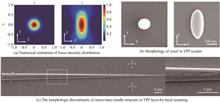
Micro-nano needle structure with continuously gradient morphology has the capacity of generating asymmetric Laplace pressure, simulating mechanical environment in nano newton grade, adjusting the ion migration rate etc., therefore, it has been widely applied in many fields such as microdroplet manipulation, biosensors, and ion rectification. However, in the previous fabrication of micro-nano needle structures with Two-Photon Polymerization (TPP), the structures were mainly constructed through the layer-by-layer scanning of laser focus. The bottom diameter or the height of the needle structure was usually in the grade of several or hundreds of micrometers. Further, the processing accuracy of the needles was generally in the grade of 100 nm, which resulted in the discontinuous morphology of the needle structures. On the other hand, the bottom diameter and structure height of micro-nano needle structures based on laser ablation or laser-assisted processing could be several micrometers, and the tip diameter could be less than 100 nm, however, the morphology and distribution of the needle structures were highly random. Considering the problems of precision, morphology and controllability in the previous fabrication of micro-nano needle structures, this paper proposes a novel method utilizing single voxel of femtosecond laser two-photon system to creating micro-nano needle-shaped structure with continuously changing morphology. In this methodology, a one-dimensional inclination angle is brought in the platform to automatically and linearly adjust the laser voxel to axially sink into the substrate completely as the stage is horizontally scanning. Finally, a micro-nano needle structure with continuous gradient morphology is produced. It is well known that, the voxel size in two-photon processing is the joint action of laser power, exposure time, scanning speed, and photoresist properties etc., the voxel might have similar size with different processing parameter combinations. Therefore, in this methodology, the size of the voxel should be calibrated firstly, and then people can determine the incline angle and corresponding processing parameters for the fabrication of needle-shaped structures. In order to facilitate the analysis of the processing results, in this investigation the scanning speed and the composition of photoresist materials are constant, and the laser power at the entrance pupil or inclination angle is selected as the variable to prepare micro-nano needle structures with different sizes. The TTP system in the experiment is built up based on femtosecond laser with a center wavelength of 800 nm. The photoresist is prepared with DETC as the initiator and PETA as the monomer. A single-axis goniometer stage, which is mounted on high precision nano stage, is utilized to configure the inclination angle of the sample. In the calibration, the laser power at entrance pupil is tuned to 3, 4, 5, 6, and 7 mW to produce the voxels with 50 ms exposure time. The lateral width of the corresponding voxels are 294, 478, 542, 621, 668 nm respectively. Meanwhile, the axial width of these voxels are respectively 720, 1 151, 1 561, 1 841, 2 060 nm. The increasing rate of lateral and axial line width will decline with the increase of power. Then, in the micro-nano needle structure fabrication, the center of the laser focus is located on the surface of the substrate at the beginning of fabrication. The incline angle is set to 1° and the platform scanning speed is 10 μm/s for scanning. A series of micro-nano needle structures with controllable length and gradually changing morphology are fabricated with fore-mentioned laser configurations. The SEM images show that the micro-nano needle structures with length of 17.3, 29.8, 40.4, 49.7, 58.1 μm are successfully obtained based on this method, which are slightly shorter than the theoretical fabrication length. It is probably caused by the declined in the concentration of the radical. As the focus gradually sink into the substrate, the effective laser intensity for exciting free radicals will decrease and lower the concentration of free radicals. Therefore, the voxel size will be reduced and result in a shorter length of micro-nano needle structure. At the same time, when the laser power is 4 mW, the inclination angles are 1°, 1.5°, 2°, and 2.5°, and other parameters are constant, the experiment fabricated structure length is consistent with the theoretical calculation. On the other hand, the topographic change gradient is positively correlated with inclination angle. It is also found that, the lateral line width of the micro-nano needle-shaped structure changes gently at the beginning of the fabrication, and changes quicker near as approaching to the end. This variation trend is determined by the structural characteristics of the single voxel, however, it does not affect the change continuity of the overall structure. The morphology change of the micro-nano needle in lateral direction is continuous in SEM observation. Further, it is seen from the AFM scanning results that benefiting from the processing principle of this fabrication methodology, the micro-nano needle structure exhibits a high-linearly gradient in height. The gradient fluctuation of the nano tips is in the order of several nanometers, and the minimum height of the nano tips could reach 5 nm. By using AFM calibration, the morphology of the nano tips are exhibited. The lateral line width gradient of the tip structure is smooth, and there are no step-like jump points. The minimum line width of the nano tips reaches 195 nm. It is noticed that, the nano tip structure changes faster in axial direction than lateral direction due to the shape feature of the voxel. In conclusion, the methodology that proposed in this work is effective and convenient for fabricating the micro-nano needle structures with high accuracy. The morphology of the experimentally fabricated needle structures are continuously gradated, and the precision of the fabrication achieved at the nanometer level. In addition, the experimental results are in high consistent with the theoretical predictions. It is worthy to mention that, the size of the TPP processing voxel can be further optimized by adjusting factors such as laser power, exposure time, photoresist, etc., which could produce finer and sharper nano tip structures. Such structures have potential applications in functional surfaces, micro-nano fluidics, and biosensing and other research fields.
Oct. 25, 2022Vol. 51 Issue 10 1014001 (2022)
Applications of Femtosecond Four-wave Mixing in Ultrafast and Ultraintense Laser Technology(Invited)
Peng WANG, Yaping XUAN, Yilin XU, Xiong SHEN, Shunlin HUANG, Jun LIU, and Ruxin LI
With the development of Chirped-pulse Amplification (CPA) and Optical Parametric Chirped-Pulse Amplification (OPCPA) techniques, ultrafast and ultraintense laser pulses can generate extreme physical conditions at lab such as ultrafast time, ultraintense electric field, ultrahigh magnetic field, ultrahigh temperature and ultrahigh pressure, which makes ultrafast and ultraintense laser pulses one of the most powerful tools to extend human's knowledge of the physical world. In the development of ultrafast and ultraintense lasers, femtosecond four-wave mixing process which is a third-order process and does not need anisotropic nonlinear crystals plays an important role in many aspects. Here, the development and application of femtosecond four-wave mixing processes on ultrafast and ultraintense laser pulses are discussed. Femtosecond pulses from Ultraviolet (UV) to Near-infrared (NIR) can be generated based on the Cascaded Four Wave Mixing(CFWM), which is of great significance in ultrafast spectroscopy, ultrafast microscopy and high temporal contrast seed pulse generation. By manipulating the spectral dispersion property, the polarization property, the spatial phase, or the crossing angle of the input beams, the CFWM signal with interesting properties can be generated. In this review article, the generation of spatially separated multicolored femtosecond sidebands from UV to NIR, the generation of high-performance seed pulses with high temporal contrast based on the CFWM or self diffraction process, and the generation of multicolor concentric annular ultrafast vector/vortex beams are demonstrated. Furthermore, based on the four wave mixing process, the generation of broadband ultrashort light pulses from narrowband seeds in transparent media can be realized. Broadband light pulses with a spectral width of hundreds of nanometers can be generated with narrowband light pulse seeds. Cross-correlator is the main method for high-dynamic single-shot temporal contrast measurement for the ultrafast and ultraintense laser pulses. Benefiting from excellent temporal domain filtering and high-energy signal generation of four-wave mixing, a single-shot Fourth-order Autocorrelation (FOAC) which consists of a four wave mixing process and a sum-frequency mixing process is developed. The signal of the self-diffraction process, or XPW process is used as the sampling pulse of the FOAC. And the stable devices with high dynamic range, wide time window, high temporal resolution, excellent measurement fidelity are combined in the proposed FOAC device, which can be helpful to investigate the temporal contrast property of high power laser pulses and realize better laser-matter interaction research. The Self-referenced Spectral Interferometry (SRSI) method with high time resolution of as high as 20 fs can also be used for the single shot temporal contrast measurement. However, the dynamic range is limited by the signal-to-noise ratio of the detector. To further improve the dynamic range, novel temporal contrast reduction techniques are proposed. The proof-of-principle experiments applying single stage of pulse stretching, anti-saturated absorption, or optical Kerr effect successfully reduce the temporal contrast by approximately one order of magnitude. The dynamic range characterization capability of the SRSI method is improved by about one order of magnitude to 109.To characterize the temporal profile of femtosecond pulses, the SRSI method is also an analytical, sensitive, accurate, and fast method. We have developed the Self-diffraction Effect-based SRSI (SD-SRSI) and Transient-grating (TG) Effect-based SRSI (TG-SRSI) for temporal profile characterization. The characterization of sub-10 fs pulse with a center wavelength of 1.8 μm is demonstrated. On the basis of the TG effect, the SRSI and the Frequency-resolved Optical Gating (FROG) are combined together to further extend the measurement ability. Weak sub-nanojoule pulses from an oscillator are successfully characterized using a TG-SRSI device, and the optical setup of which is smaller than the palm of a hand. The compactness of the SISR device makes it convenient to use in many applications, including monitoring the pulse profile of laser systems as a sensor. In the future, the femtosecond four-wave mixing processes can be extended to the EUV and THz spectral ranges, which will extend the application range of ultrafast and ultraintense laser technology.
Oct. 25, 2022Vol. 51 Issue 10 1014002 (2022)
Tianqi WANG, Duidui LI, Beibei LIU, Man JIANG, Zhipei SUN, and Zhaoyu REN
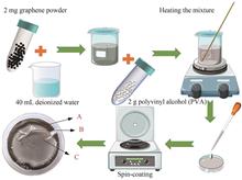
Q-switching is a technology that converts continuous light into pulse light to obtain high pulse energy and peak power. It is widely used in material processing, biomedicine, nonlinear frequency conversion and other fields. Generally, Q-switching can be divided into passive and active mechanisms. The passive Q-switching is achieved by inserting a saturable absorber into the cavity. Its structure is simple, but the repetition frequencies of the output pulses depend only on the pump power. Active Q-switching uses external drive electro-optic and acousto-optic modulator to adjust the Q factor of the laser to achieve pulse output. These types of Q-switching system can flexibly control the change of pulse repetition rate, but it breaks the all-fiber structure and leads to a high cost. More importantly, the modulator needs to be specially designed because of the narrow working bandwidth. However, we are inspired by the graphene all-optical modulator, which can regulate the attenuation of the specific light in graphene by introducing another frequency of light into the graphene, thus regulating the in-cavity Q factor. In addition, graphene acts as a saturable absorber in the laser cavity. Therefore, we have built an active-passive Q-switched fiber laser based on graphene all-optical modulator, which can not only obtain stable narrow pulse, but also flexibly change the repetition frequency without changing the pump power. It has an all-fiber structure and a wide working bandwidth. At the same time, we also studied the effects of different modulation depths of graphene on the pulse repetition rate and pulse width variation range. Here, the graphene-films are made by spin-coating the graphene Polyvinyl Alcohol (PVA) water solution, which are placed between two fiber connectors to form graphene modulators. We measured the modulation depths and saturation strengths of three graphene (A, B, C), of which the modulation depths are 33.5%, 18.1% and 8.7%, corresponding to saturation strengths of 40, 5.4 and 3.5 MW/cm2, respectively. Then, we built an active-passive Q-switched fiber laser, which consists of an active modulated light with a wavelength of 1 310 nm and a passive Q-switched Erbium-doped ring cavity fiber laser with a wavelength of 1 560 nm. First, a passive Q-switching pulse with a repetition frequency of 18.7 kHz and a pulse width of 10.3 μs is obtained when the active modulated light is turned off. After that, we turned on the modulation light and set the repetition frequency of the modulation light to 18 kHz, and obtained a output pulse with a repetition frequency of 18 kHz and the pulse width of 6.34 μs. It can be seen that the repetition frequency of the output pulse is controlled by the repetition frequency of the modulated light, and the output pulse width is significantly narrower than the passive Q-switched pulse width. Further study shows that the output pulse width gradually widens with the increase of the modulation repetition frequency, while the pulse energy and peak power decrease, which is attributed to as the modulation frequency increases, the energy stored in the gain fiber per switching cycle reduces and therefore releases longer pulse with lower pulse energy. The experiment also explored the effects of three graphene films with different saturation strengths on the repetition frequency and pulse width variation range of the output pulse at different pumping powers. It shows that when the modulation depth of graphene modulator is larger, the variation range of output pulse repetition rate is larger, the variation range of output pulse width is smaller, and the maximum variation range of repetition rate is 31.6 ~92.6 kHz. The modulator described in this paper is easier to be integrated into optical system than the traditional modulator, and has a broad application prospect in nonlinear frequency conversion, multi-color pump detection spectrum and other fields. At the same time, the research also provides a reference for selecting suitable graphene films in the field of Q-switched lasers.
Oct. 25, 2022Vol. 51 Issue 10 1014004 (2022)
Shunyu YANG, Jingfeng ZHOU, Ben LI, and Yang BAI
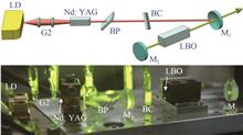
A Laser Diode (LD) pumped Nd: YAG crystal low-noise all-solid-state yellow-green laser in the wavelength range of 555~561 nm is reported, which becomes as a research hotspot because of its great application potential in industry, atmospheric remote sensing, communication, information storage, food and drug detection and other fields. As we all know, noise is one of the key indicators to measure the stability of laser output. The power stability of the low noise laser beam is higher because there are no power transient spikes. However, the Nd: YAG crystal excites three spectral lines simultaneously at 1 112.62 nm, 1 116.70 nm and 1 123.24 nm. The mode competition among the three spectral lines, the mode competition among the different longitudinal modes in each spectral line and the three-wave coupling effect of the frequency doubling process all make that the frequency doubled yellow-green laser has strong noise and low power stability. It is very difficult to realize that any one of the above-mentioned three spectral lines with very short wavelength interval oscillates individually in the cavity by the method of coating a narrow-band reflective film. At present, the common method to reduce the noise of all-solid-state yellow-green laser is to insert an etalon with the function of selecting a single longitudinal mode or a Birefringent Crystal (BC) with a filtering function into the linear cavity. However, the fundamental frequency laser oscillating in the linear cavity has the inherent defect of small mode volume, which is not conducive to obtaining high power frequency doubled yellow-green laser. The use of etalons to eliminate mode competition among multiple longitudinal modes usually comes at the expense of the output power and the optical-to-optical conversion efficiency of the laser. When performing frequency selection and filtering with a BC placed according to the Brewster angle, it is usually necessary to precisely adjust the size of Brewster angle and the angle between the optical axis of the fundamental frequency laser and the surface of BC. Therefore, it is extremely difficult to obtain a high-power yellow-green laser using a compact cavity.In this paper, an all-solid-state yellow-green laser with wavelength-adjustable in the range of 555~561 nm, high power and low noise is reported. A folded cavity structure based on an 808 nm LD end-pumped Nd: YAG crystal and a type-I angle-matched LBO crystal intracavity frequency-doubling is used. After optimizing the structural parameters of the cavity, the coupling rate between the mode volume of the fundamental frequency laser and the mode volume of the LD pump laser is improved, and the cavity had the thermal insensitivity to the dynamic change of thermal focal length. In addition, the beam astigmatism caused jointly by the folded cavity structure and the concave mirror is also effectively compensated. A Brewster Polarizer (BP) and a BC are successively inserted into the cavity to form a Birefringent Filter (BF). After precisely adjusting the corresponding Brewster angle of the BP, respectively, the frequency selection for the three spectral lines with wavelengths of 1 112.62 nm, 1 116.70 nm and 1 123.24 nm generated by Nd: YAG crystal is completed. Meanwhile, the oscillation of a single wavelength fundamental frequency laser is realized in the cavity on the basis of precisely controlling the pitch angle of the cavity mirror. Then, the filtering of the fundamental frequency laser (i.e. the number of compressed longitudinal modes) is realized by adjusting the angle between the p-polarization direction of the fundamental frequency laser and the optical axis of BC. Finally, high-power, high-stability, and low-noise yellow-green laser with central wavelengths of 556.31 nm, 558.35 nm, and 561.62 nm is obtained, respectively, which is based on the I-type angle-matched LBO crystal intracavity frequency doubling. When the highest pumped power of LD is 8.0 W, the maximum independent CW output powers of the yellow-green laser beams with central wavelengths of 556.31 nm, 558.35 nm and 561.62 nm reach 678 mW, 653 mW and 606 mW, respectively, corresponding to the optical-to-optical conversion efficiency are 8.47%, 8.16% and 7.58%, and the line widths are 0.34 nm, 0.42 nm and 0.37 nm, respectively. At an output power of 500 mW, the power instability of the three yellow-green laser beams at 556.31 nm, 558.35 nm and 561.62 nm are ±0.42%, ±0.38% and ±0.49%, respectively, the corresponding SMR noise are 0.69%, 0.51% and 0.96%. Meanwhile, the beam quality factor are (M2x-556.31 = 3.943, M2y-556.31 = 4.301), (M2x-558.35 = 3.409, M2y-558.35 =3.584) and (M2x-561.62 = 3.732, M2y-561.62 = 3.971), respectively.The experimental results show that the frequency selective filtering of “BP+BC” is an effective method to realize high-power, high-stability, low-noise, wavelength-adjustable yellow-green laser. Our research provides a novel source for future potential applications in biomedicine, laser measurement, pollution monitoring and spectral analysis.
Oct. 25, 2022Vol. 51 Issue 10 1014005 (2022)
Junyi MA, Guodong ZHAO, Xiaodong SHAO, Hainian HAN, and Zhiyi WEI
Great emphasis has been placed on the development of GHz femtosecond lasers for the Yb-doped All-Solid-State Laser(ASSL) that has important application values in many fields such as precision measurement. Compared to general femtosecond oscillators with repetition frequencies in the tens to hundreds of megahertz,GHz femtosecond pulse has been demonstrated to have larger spacing between adjacent longitudinal modes and higher single longitudinal mode power. This GHz repetition frequency femtosecond oscillator is realized by passive mode-locking techniques, including Semiconductor Saturable Absorption Mirror(SESAM) and Kerr Lens Mode-locking(KLM). The latter has the following advantages: simplicity, very fast response, self-starting and self-sustaining. Ytterbium-doped gadolinium calcium chlorate (Yb:CaYAlO4, referred to as Yb:CYA) crystal has the advantages of easy growth, broad and flat gain curve, high specific heat capacity, good thermal conductivity, etc. It is an excellent dielectric crystal for generating femtosecond ultrashort pulses.Femtosecond laser pulses based on Yb:CYA crystals were first reported in 2011. In 2018, MA Jie et al. of Jiangsu Normal University reported that the shortest pulse width of Yb:CYA oscillators was 21 fs with the help of two SF10 prisms, while the highest output and peak power achieved by Yb:CYA crystals was experimentally realized by TIAN Wenlong et al. from Xidian University. The Yb:CYA optical frequency comb debuted in 2016, demonstrating the first Kerr lens mode-locked solid-state optical frequency comb in the 1 μm band. In 2019, the author's research group achieved for the first time that a watt-scale solid-state Yb:CYA femtosecond laser frequency comb is fully locked to the carrier envelope phase shift frequency and repetition frequency, with a pulse width of 54 fs and an average power of 1.5 W. The free-running carrier-envelope offset (fceo) was observed with a signal-to-noise ratio of 40 dB at 100 kHz resolution bandwidth, and the residual phase jitter of the fceo after locking was only 370 mrad. When the duration is 3 hours and the counting gate time is 1 s, the standard deviation of fceo long-term frequency drift is only 0.8 mHz.In this paper, an all-solid-state Kerr lens mode-locked GHz femtosecond oscillator based on Yb:CYA crystal is introduced. A 980 nm fiber laser with a power of 8 W is used as the pump source, and the cavity type is a four-mirror ring cavity structure. In our experience the ring cavity has the advantages of stable mode locking, relatively insensitive to optical feedback, reducing the dispersion in the cavity and high repetition frequency compared with the linear cavity configuration. The transmission of the output coupler is 1.6%. The 3 mm Yb:CYA crystal is wrapped with indium foil and mounted in a copper block that is cooled by using a water cooler with temperature feedback to maintain a constant 13℃ temperature, and the sample is antireflection-coated for both the pump and laser wavelengths from 970 nm to 1 200 nm. The initiation of the mode locking is observed by a fast oscilloscope, and the oscillator is capable of generating GHz femtosecond pulses with a center wavelength of 1 051 nm and an average output power of 1.7 W with a pulse duration of 207 fs. The Radio Frequency(RF) spectra measurement shows that the fundamental frequency of the signal is about 1.02 GHz with a Resolution Bandwidth (RBW) of 100 kHz, spanning 5 MHz. The Signal-to-noise Ratios (SNR) is 50 dB, suggesting that the unidirectional KLM runs stably.To the best of our knowledge, this is the first time that an oscillator based on Yb:CYA crystal has achieved GHz repetition frequency watt-level femtosecond pulse output, which lays a solid foundation for further realization of high repetition frequency femtosecond optical frequency combs based on this oscillator.
Oct. 25, 2022Vol. 51 Issue 10 1014006 (2022)

Zixin WANG, Ningning DONG, Lulu WANG, Xun CAO, and Jun WANG
Semiconductor-metal phase transition in metal oxides have attracted much attention due to their scientific significance in condensed matter physics and their possibilities in a variety of applications. During the last half century, experimental and theoretical studies on phase transition mechanism have been discussed. Vanadium dioxide (VO2) has attracted much attention due to its phase transition properties at room temperature. The VO2 phase transition can be triggered by a variety of excitations, such as thermal, electrical, optical, magnetic field, and strain, and because the phase transition process is reversible and its optical properties change significantly, it is widely used in optical switches, smart windows, optical storage, and laser protection. With the rapid development of femtosecond laser technology, more and more researchers are involved in the study of laser-material interactions. The control of VO2 phase transition on ultrafast time scale using optical means will benefit its potential applications in memory devices, ultrafast optical switches and bistable optoelectronic devices.Firstly, we briefly introduce the basic properties of VO2. The material undergoes a phase transition at room temperature (~68°C), which is reversible and non-destructive. Stimulated by external conditions, VO2 transforms from a monoclinic semiconducting phase (P21/c) to a tetragonal rutile phase (P42/mnm) with a distortion of the lattice structure, accompanied by a change in electrical resistance of about four orders of magnitude and a consequent change in its optical properties. A common method for inducing semiconductor-metal phase transition is thermal triggering. Below the phase transition temperature, VO2 is a semiconducting phase with a high transmittance, and when the temperature is heated above 68°C, VO2 changes into a metallic phase with abrupt changes in its optical properties such as refractive index, transmittance, and reflectance. The phase transition can also be triggered on sub-picosecond time scales under femtosecond laser induction. Due to the extremely high response rate and significant optical property changes of laser-induced phase transition, it is important to study the laser-induced phase transition process, which will help to expand its applications in optical devices and systems.Secondly, we prepared VO2 film using magnetron sputtering, a kind of physical vapor phase deposition which is widely used for the synthesis of VO2 thin films due to high deposition rate, uniform film formation, high reproducibility and suitable for large area preparation. The Atomic Force Microscope (AFM) image clearly shows the surface morphology of the sample, which is found to be uniform with a high flatness, and the thickness of the sample is ~195.5 nm. The XRD pattern shows a distinct diffraction peak at 2θ = 40°, corresponding to the (001) crystal plane, indicating that the sample is a well crystallized pure phase VO2(M). A typical thermogenic echo line is observed in the temperature-dependent transmittance curve, with the most pronounced change in transmittance near the phase change temperature, which drops sharply from ~42.1% to ~11.6%. The sample recovery temperature is at ~53 ℃ with an average hysteresis of ~15 ℃.Thirdly, the optical response of VO2 film under femtosecond laser induction was measured using a home-built transmission and reflection I-scan experimental setup. As the incident laser intensity increases, the sample changes of transmittance and reflectance show four different stages: nonlinear absorption process, phase transition process, steady state process and damage process. At lower laser intensities (less than ~26.2 mJ/cm2), the VO2 film maintains a high transmittance, showing a slight decrease from 43.9% to 40.3% with increasing laser intensity, while the reflectance remains essentially constant at ~6.3%, indicating that the sample does not undergo a phase change and remains in the semiconducting phase. This change is mainly attributed to the two-photon absorption process of the VO2 semiconductor. When the laser intensity reaches ~26.2 mJ/cm2, the sample transmittance suddenly decreases from ~40.2% to ~12.8%, while the reflectance sharply increases from ~6.6% to ~12.0%, which is the result of the laser-induced phase transition of VO2 from the semiconducting phase to the metal phase. Compared with the temperature-induced transmittance change in VO2, the same effect can be achieved by laser-induced, and it can be inferred that the phase change induced under the laser action is caused by the laser thermal effect. The steady state process is that the transmittance and reflectance remain in relative equilibrium after the sample phase changes to the metallic phase without significant change. When the laser intensity rises above ~104.4 mJ/cm2, the transmittance of the sample starts to decrease, and the reflectance also starts to decrease after a slow increase, which is due to the thermal damage of the sample under the laser action. In order to further analyze the change process of optical properties of VO2, especially the phase change mechanism of laser thermal effect, the transmittance (T) and reflectance (R) as a function of laser intensity are measured at different laser repetition frequencies, and calculated the sample absorbance (A) using the equation A = 1-R-T. The experimental results at all laser repetition frequencies show the four stages of laser-induced VO2. With the increase of the repetition frequency, the laser-induced phase transition turn-on threshold decreases from ~45.4 mJ/cm2 to ~1.3 mJ/cm2 and the damage threshold decreases from ~176.8 mJ/cm2 to ~5.9 mJ/cm2. The laser thermal effect is enhanced and the thermal accumulation of the sample increases due to the increase of the laser repetition frequency, leading to more susceptible to phase transition and damage.Finally, a brief summary of the work is given, and we expect that this study will have a contribution to the further development of this material in the field of optics.
Oct. 25, 2022Vol. 51 Issue 10 1014007 (2022)
Hongxiang LIN, Xiaohui WEI, Tianfa LIAO, Wenyuan WANG, Juan DU, and Mingliang YANG
Free electron laser light source is a new type of coherent light source. It has many advantages such as wide wavelength range, pure spectrum, high power and so on. It has significant application requirements in biology, materials, medicine and other fields. Therefore, since the invention of free electron laser theory in the 1970s, free electron laser technology has been developed rapidly. The principle of free electron laser is to make use of electron beam oscillation in periodic electromagnetic field to produce electromagnetic radiation. By controlling the oscillation period, the magnetic radiation light forms coherent radiation. The undulator is a key technical component of free electron laser, which is used to generate the periodic electromagnetic field that oscillates the electron beam. At present, the undulator is usually composed of magnets, and uses magnetic field to realize deflection oscillation of electron beam, coupling the energy of electron beam to the laser field. In 1988, researchers at the Institute of High Energy Physics of the Chinese Academy of Sciences proposed a free electron laser scheme based on ferroelectrics generating transverse deflecting electric fields. Nearly 30 years, laser technology and processing technology have obtained fast development, leading to a series of micro accelerator innovation, with many new accelerators constantly emerging, such as metal surface laser accelerators and medium-sized laser accelerators, and a large number of researchers around the world constantly promoting micro accelerator technology forward. Inspired by lateral deflection field free electron laser solutions, and benefit from the development of laser, micro-nano technology in recent years, this paper puts forward a kind of miniature undulator, based on the structure of grating with femtosecond laser pulses irradiation grating. The periodic transverse deflection electric field is formed on the surface of the grating, and the high energy electron beam is modulated by the periodic electric field, which generates periodic oscillation and radiates coherent electromagnetic wave to form a gain of free electron laser. In this paper, the free electron laser vibrator with grating structure is theoretically analyzed, the trajectory equation of electron beam is given, and the electric field simulation of the structure is carried out to obtain the transverse electric field distribution on the surface of the grating. Finally, a 10 MeV electron beam with 10 mA intensity is tracked, and the laser gain is calculated.
Oct. 25, 2022Vol. 51 Issue 10 1014008 (2022)
Xuewen WANG, Zhengyan XU, Kaige WANG, Zhiyong ZHANG, and Wu ZHAO
With the increasing application of biosensors, the development of new biosensors has become an important strategy for the development of science and technology in the world. Scientists have cross-infiltrated nanotechnology and biotechnology to form nanobiotechnology, and develop nanobiosensors. Compared with traditional biosensors, due to the enhanced electron transfer kinetics and strong adsorption capacity of nanomaterials, it provides higher stability for bioelectrodes, high surface-to-volume ratio for higher biomolecule loading, and a high level of stability for the bioelectrode. Biomolecules including enzymes, antibodies, microorganisms, DNA and other proteins can be immobilized to provide a suitable microenvironment. Therefore, nanomaterials can not only greatly improve the detection sensitivity of the sensor, but also provide a theoretical basis for the analysis of single molecule activity. The combination of nano and biology can also improve clinical efficacy and improve biological species, which can be used for microbial detection, monitoring of body fluids metabolites, and early detection of tissue lesions such as tumors. As a direct wide-bandgap semiconductor, ZnO has been used in electronic devices, optoelectronic devices, biosensors and other fields due to its excellent properties such as non-toxicity, good biocompatibility, stable physical and chemical properties, and it can take advantage of its high isoelectric point to bind and immobilize biomolecules with low isoelectric points such as proteins through electrostatic adsorption interactions. In particular, the research of biosensors based on nano-ZnO has become a new hot spot in the field of epidemic prevention and medical treatment. In this paper, we introduce several main preparation methods of nano-ZnO (including hydrothermal method, magnetron sputtering method, sol-gel method and atomic layer deposition method, etc.), their advantages and disadvantages, the excellent properties of the as-prepared ZnOs and the methods to enhance their properties (such as process optimization, doping, recombination, heterojunction, etc.) are comparatively analyzed. The article focuses on the application of nano-ZnO materials in the field of biosensors. The various unique advantages of ZnO nanomaterials enable different types of biomolecules to be successfully immobilized on their surfaces, so they have broad application prospects in the field of biosensors. The analytes most commonly used as detection materials include: lower molecular weight molecules(dopamine, uric acid, urea, and riboflavin), proteins(bovine serum albumin, immunoglobulin, streptavidin), nucleic acids(RNA, DNA), cells(cancer cells, infected cells), bacteria and many more. According to the different working principles of their signal processing components, the biosensors prepared by ZnO nanomaterials are divided into electrochemical sensors, optical sensors and field effect transistor sensors, and the use of new technologies such as piezoelectric ZnO nanobiosensors, ZnO biosensors chip and so on. Then the chitosan film is formed and fixed on the glassy carbon electrode. The hydrogen ion concentration index electrode is an electrochemical sensor widely used in blood glucose meters. The glucose sensing of vertically grown ZnO nanorods combined with chitosan is investigated. And we introduce their structures, working principles and their outstanding performance and development status for biological detection in detail respectively. Finally, we prospect and summarize the current challenges and future development trends of nano-ZnO biosensors.
Oct. 25, 2022Vol. 51 Issue 10 1016001 (2022)
Qianqian SHI, Jiang WANG, and Guanghua CHENG
Vanadium dioxide (VO2) has attracted many attention of researchers since it was discovered in 1959 to have the reversible phase transition from metal to insulator. Before and after the phase transition, its optical, electrical and thermal properties change dramatically. Therefore, vanadium dioxide is widely used in the fields of thermal light control, infrared and optical protection camouflage, ion batteries and chemical sensors. In order to enable domestic researchers to have a more comprehensive and in-depth understanding of this interesting material with broad application prospects, this paper reviews the latest progress of vanadium dioxide film preparation technology in the past five years and its applications in different hot areas.First, we introduce the structure and phase transition mechanism of VO2. When the temperature exceeds 68℃, VO2 will undergo a phase transition from insulator to metal, and its crystal structure will change from monoclinic insulator to rutile metal structure. At the same time, because the crystal structure of vanadium dioxide changes after phase transformation, its corresponding energy band structure also changes. Because the crystal structure and energy band structure of VO2 change suddenly before and after the phase transition, people devote themselves to exploring the physical mechanism of its phase transition. Up to now, there have been many research on the VO2 phase transition mechanism, and also various research methods and devices, but there is no accurate and unified statement. In this paper, we focus on three mainstream explanations of phase transition mechanisms: the first is electron-electron correlation mechanism, i.e. electron correlation driven Mott transition; The second is the electron phonon interaction mechanism, i.e. crystal structure driven Peierls transition. The third is that electron correlation and crystal structure jointly drive VO2 phase transition, and the supporting evidence is summarized. In addition, the phase transition characteristics of vanadium dioxide films are closely related to the preparation technology and process parameters.In the second part of this paper, many new technologies for preparing VO2 thin films, such as high-energy pulsed magnetron sputtering, atomic layer deposition, ink-jet printing, spray pyrolysis and laser direct writing, are introduced in detail, and the advantages and disadvantages of each technology are briefly described. This part provides ideas for researchers on the preparation of materials at the initial stage of experimental design.In performance evaluation, this parameter thermal hysteresis width ΔH reflects the excellent degree of phase transition characteristics of VO2 thin films ΔH will attenuate the phase transition behavior, reduce the working efficiency of the uncooled detector, and also reduce the sensitivity of the near-infrared optical response to temperature, thus reducing ΔH is of great significance for the wide application of VO2 thin films in optoelectronic devices. The third part of this paper focuses on the regulating of the thermal hysteresis width ΔH. Many factors, such as stress, doping and defects, are analyzed. The stress factor is mainly reflected in the selection of substrate materials when preparing films. Different substrates will produce films with different orientations, and different orientations will show different properties. Both doping and oxygen defects change the phase transition properties of the materials by distorting the lattice of the materials in the films.The performance of materials determines the width of their application prospects. VO2 suddenly changes optical, electrical and other properties before and after phase transition, so it is widely used in optoelectronic devices. In recent years, the combination of VO2 thin films and two-dimensional super surface structures is also a hot direction of application. In this paper, we mainly introduce the application of VO2 thin films in the fields of modified smart windows, terahertz modulators, ultrafast optical switches, electrode materials and various sensors. This part can provide inspiration for researchers to explore new applications of VO2 materials.Finally, the problems and prospects faced by the development of VO2 thin films are predicted and evaluated. 1) How to prepare high-purity VO2 thin films. 2) How to reduce the phase transition temperature without reducing the phase transition performance. The solution of these two problems can contribute to the perfect application of VO2 materials in military, laser, and other integrated equipment systems. We sincerely hope that this paper will contribute to the development of new active materials and devices in the field of optoelectronics.
Oct. 25, 2022Vol. 51 Issue 10 1016002 (2022)
Qingyan HAN, Yunxiang LI, Wei GAO, Wenwen ZHANG, Xuewen YAN, Enjie HE, Lipeng ZHU, Zhiyu ZHANG, Fengtao HE, Jiamin GONG, and Jun DONG
With the rapid development of nanotechnology, various noble metal nanomaterials with multiple functions have been designed and developed, which have attracted broad research attention due to their unique physical properties and wide applications in catalysis, sensing, photothermal therapy, and surface-enhanced spectroscopy. As is well known, Localized Surface Plasmon Resonance (LSPR) response of noble metal nanomaterials including gold (Au), silver (Ag), and copper (Cu) are dependent on their type, morphology, structure, size, and dielectric function. Many attempts have been devoted to synthesizing and adjusting the morphology and dimension of noble metal nanostructures. Ag nanomaterials have good surface plasmonic properties due to their proper electronic structure and dielectric function. Unfortunately, Ag nanostructures have poor chemical stability, which seriously hinders their further applications. In contrast, Au nanoparticles (NPs) have better stability, but their catalytic activity is related to the size of NPs. Therefore, simultaneously obtaining higher-quality plasmonic and catalytic properties in single nanostructure with good chemical stability remains a hotspot issue. We report a facile wet chemical technique for fabricating AuAg alloy nanoparticles (ANPs) with high dispersibility, which integrate high stability, controllable plasmonic property, and excellent catalytic activity. A series of characterizations confirm the structure and compositional homogeneity of AuAg ANPs. Firstly, Transmission Electron Microscopy (TEM) image reveals the monodisperse nature of the as-synthesized AuAg ANPs with an average diameter of ≈ 35 nm, which indicates the purity and uniformity of the NPs. Then, Selected Area Electron Diffraction (SAED) image exhibits three clear diffraction rings that are corresponding to (111), (200), and (220), respectively, providing evidence that AuAg ANPs have multi-crystal nature. It is worth mentioning that some bright spots in the diffraction rings are found in the SAED picture, which mainly results from the (111) and (200) faces of the AuAg ANPs. This result further confirms that the AuAg ANPs belong to a polycrystalline crystal structure. Energy-dispersive X-ray (EDX) elemental mappings prove that the elements existed in the sample are uniformly distributed in the entire ANPs, and the compositions of the typical AuAg ANPs are consisted of Au and Ag. In addition, UV-visible-NIR absorption spectra of Ag NPs, Au1Ag3 ANPs, Au1Ag1 ANPs, Au3Ag1 ANPs, and Au NPs are detected to investigate their plasmonic properties. It is found that the surface plasmon resonance peaks of AuAg ANPs could be effectively regulated by changing the molar ratio of Au and Ag. When the content of Ag is decreased in AuAg ANPs, the surface plasmon resonance peaks of AuAg ANPs will be red-shift, in which experimental results are consistent with the theoretical ones. Finally, the catalytic performance of AuAg ANPs is also studied by choosing a model of chemical reduction of p-nitrophenol (4-NP) by using NaBH4. It is well known that NaBH4 individual cannot reduce 4-NP in the absence of any catalyst, which indicates the need of a catalyst for the chemical reduction of 4-NP. The reduction process is monitored by UV-Vis spectroscopy. The reaction kinetics follows pseudo first order reaction and the variations of 4-NP concentration (Ct/C0) in the noble metal NPs with different reduction times are calculated. The corresponding results reveal that the catalytic activities of AuAg ANPs are much better than that of Au NPs and Ag NPs due to the synergistic effect between Au and Ag species at room temperature. What's more, the catalytic property of Au3Ag1 ANPs is the best among three kinds of ANPs. The objective of the current strategy may provide a new idea for constructing the higher-performance alloy nanostructures and developing a potential application in the treatment of aromatic nitro organic pollutants, sensing, and solar cells.
Oct. 25, 2022Vol. 51 Issue 10 1016003 (2022)
Lu XIN, Wen XIAO, Yakun LIU, Huanzhi ZHANG, Xiaoping LI, and Feng PAN
Radiotherapy and chemotherapy are essential for preoperative and postoperative treatment of cancer patients. Chemotherapy drugs destroy cancer cells and inhibit their proliferation mainly by promoting cancer cell apoptosis. The efficacy of anticancer drugs is measured by their ability to recognize cancer cells and selectively promote their apoptosis. The Drug Sensitivity Test (DST) is a method to determine the most effective drug for tumor treatment according to the sensitivity. Tumors may be resistant to one or more drugs, or show sensitivity to multiple drugs for their different genotype and pathogenesis. Therefore, the detection of drug-induced apoptosis in anticancer drug sensitivity test is of great significance for reducing drug resistance, improving the efficiency of drug sensitivity test and achieving more effective personalized treatment. At present, the main methods to detect apoptosis are to detect the changes of cell morphology and surface markers related to apoptosis. However, the commonly used methods like flow cytometry, membrane protein, TUNEL analysis, have poor specificity in the detection of cell apoptosis. The typical morphological changes exhibited in the process of apoptosis which have become a reliable basis for the identification of apoptosis. Digital holographic microscopy provides a non-invasive quantitative phase imaging method for living cells. It can meet the requirements of label-free, long-term imaging, and evaluation of cell morphological and kinetic parameters under different treatments. In this paper, digital holographic microscopy is used to record images of label-free cancer cells during apoptosis process after adding drugs. Firstly, a Mach-Zehnder digital holographic microscopic system with an off-axis configuration is used to capture the wave-field of cancer cells. This system can realize complex object wavefront reconstruction with a single camera exposure. In the process of cell imaging, the cells adhere to the bottom of the cell culture dish, and the culture dish is filled with cell culture solution to ensure the normal growth of cells. The camera records a hologram every 1min for a total of 9 hours after adding drugs into the cell culture solution. Then, the phase images of cancer cells are numerically reconstructed. Two pre-processing operations are implemented, consisting of hologram apodization and spatial filtering and then the angle spectrum reconstruction algorithm is employed to implement the numerical propagation, keeping the object image size constant whatever the propagation distance. To obtain an in-focus and sharp object image, an optimal propagation distance needs to be found by automatic focus method. Besides, Numerical Parametric Lenses (NPL) method is employed to compensate the phase aberrations in the phase image. Due to the phase value reconstructed from the hologram constrained between-π and π, the continuous phase map of the object can be retrieved by phase unwrapping. From the reconstructed phase image of cells after 9 hours of drug treatment, it can be clearly seen that most of the cells have broken and died, while other cells that have not broken have also shrunk significantly, and the cell height has increased significantly. Furthermore, we select 8 cells from the dead cells for further analysis of their complete death process. Single-cell phase images are segmented from the phase images. And, the morphological change of cell apoptosis process is characterized morphologically by the average phase shift and dry mass. It can be seen from the change carves of these two parameters during the cell apoptosis, there is no obvious change of cell dry mass before apoptosis. But at the moment of the cells lose membrane integrity and release their intracellular contents, cells' dry mass decreased sharply. At the meantime, the average phase shift continuously increases before the cells lose membrane integrity, indicating that the cells have contracted, which is consistent with the conclusion in previous study. These results show that there are significant differences in phase images and morphological parameters between growing cancer cells and apoptotic and dead cells. Therefore, the method in this paper can distinguish apoptotic cells and dead cells without fluorescent labeling. And it can provide a more economical and convenient detection method for determining and selecting the most effective chemotherapeutic drugs and determining their effective dose for in vitro drug sensitivity test in individualized treatment.
Oct. 25, 2022Vol. 51 Issue 10 1017001 (2022)
Zhichao HAN, and Yiping HAN
In recent years, Terahertz-waves have brought a brand-new, label-free, non-invasive detection method to biomedical research due to their non-ionization, broadband, and high signal-to-noise ratio. With the development of Terahertz sources, especially the generation of Terahertz pulses with energy up to mJ, the study of biological tissues in Terahertz band is no longer limited to non-thermal effects. Histopathological test is considered as the gold standard for diagnosing skin cancer and other tumors. However, the borders of some tumors are blurred, which may result in excessive surgery, mistaken resection, or inability to fully resection in the process of histopathological test. It is of great value to combine the physical properties of skin tissue and Basal Cell Carcinoma (BCC) with their optical properties in the Terahertz band for the non-destructive diagnosis of skin cancer. The purpose of this paper is to provide a certain theoretical basis for the non-destructive detection of early skin cancer by studying the photoacoustic effect of Terahertz-Waves in in vivo tissues (normal skin tissue, skin tissue containing basal cell carcinoma). In this paper, according to the dendritic growth law of basal cell carcinoma in the basal layer of skin tissue, combined with the absorption characteristics of skin tissue in the Terahertz band and the difference in water content between skin tissues, a skin tissue model containing basal cell carcinoma is established. The model includes the stratum corneum, epidermis, and lesions of different basal cell carcinomas. As a control, a structural model of normal skin tissue is also established. Using the Pennes heat transfer equation, the Terahertz radiative heat effects of normal skin tissue models and skin tissue models containing basal cell carcinoma are analyzed. Finally, the differences and components of photoacoustic signals between normal skin tissue models and skin tissue models containing different basal cell carcinoma growth stages are analyzed using the photoacoustic effect of Terahertz-Waves. The simulation results show that the absorption of Terahertz-Waves in the epidermis is most obvious. It is difficult for high-energy pulsed terahertz waves to penetrate deep into the dermis for both normal skin tissue and skin tissue containing basal cell carcinoma. However, there are significant differences in thermal effects between skin tissue containing basal cell carcinoma and normal skin tissue. Skin tissue containing basal cell carcinomas is more sensitive to temperature changes from Terahertz-Waves irradiation. The analysis of different basal cell carcinoma growth stages shows that the temperature response of Terahertz-Waves could be used to detect the growth changes of basal cell carcinomas. As basal cell carcinomas spread and grow in skin tissue, it is easier to distinguish the different basal cell carcinoma growth phases by thermal effects. Furthermore, rapid diagnosis of basal cell carcinoma can be achieved by Terahertz-Waves irradiation with a single pulse energy of the order of μJ. Analysis of the difference in the photoacoustic signals between the two models shows that the skin tissue containing basal cell carcinoma produces stronger photoacoustic signals than normal skin tissue. As basal cell carcinoma spreads and grows, the photoacoustic signal received on the outer surface of the skin has a greater amplitude, and the photoacoustic signal generated by the stratum corneum and epidermis decays faster, which make it easier to detect and analyze. The findings are suitable for non-destructive diagnosis of early-stage skin cancer by Terahertz-Waves. The application value of Terahertz photoacoustic effect in the field of non-destructive test and fast real-time imaging is revealed. At the same time, it has certain significance for the selection of detectors, detection methods, Terahertz sources and suitable types of biological tissues in the experimental research of Terahertz photoacoustic imaging.
Oct. 25, 2022Vol. 51 Issue 10 1017002 (2022)
Zhanying YANG, and Yuhan WU
Breathers, nonlinear waves with periodic evolution or periodic distribution, whose shapes undergo periodic oscillations during propagation, can be localized in time or space with a finite background. Such breathers are widely found in physical systems such as nonlinear optics, fluid mechanics, Bose-Einstein condensates and PT-symmetric systems. Usually, according to the different excitation background, it can be divided into zero background and plane wave background. Among them, breathers on zero background are essentially “multi-soliton bound states”, and there are extensive experimental reports in ultrafast fiber lasers. Here we emphasize the importance of the breathers on the plane wave background of the latter case. Indeed, these breathers exhibit periodic energy exchanges with the plane wave background.Common breathers are mainly classified by their properties into Kuznetsov-Ma breather, Akhmediev breather, Tajiri-Watanabe breather, and Super-regular breather. Quite remarkably, the Akhmediev breather can be used to describe the well-known Fermi-Pasta-Ulam recurrence and higher-order modulation instability, showing the dynamic processes with doubly periodic characteristics such as regular or shifted recurrence and pulse splitting. In addition, the study of breathers is helpful to understand the phenomena including the generation of supercontinuum and turbulence in nonlinear systems. Moreover, the interactions of the breather have been shown to be useful for high-power pulse preparation and to reveal the nonlinear evolution of modulation instability.Generally, the study of the breather dynamics is mainly based on the integrable (1+1) dimensional nonlinear Schr?dinger equation. In brief, the existence and excitation conditions of different kinds of breathers are obtained theoretically by exact solution in the integrable system, and the different breather structures are obtained by using the simple initial states for evolution. On the other hand, the formation conditions of breathers can be analyzed through the excitation mechanism of different breathers, and the dynamic properties and experimental realization of breathers can be explored. At present, the theoretical and experimental results of breathers are mainly discussed from the following aspects: 1) the existence conditions of breathers in different nonlinear physical systems; 2) theoretical method for accurate solution of breathers; 3) structure and properties of breathers; 4) excitation mechanism and production conditions of breathers; 5) evolution characteristics of different breathers; 6) interaction characteristics of breathers; 7) applications of breathers in supercontinuum generation, high-power pulse preparation, etc.For nonlinear physical system, nonlinear fiber is a mature nonlinear experimental platform in experimental science. Therefore, based on nonlinear optical systems, this paper briefly discuss the experimental and theoretical research progress of several typical breathers on continue wave background. Based on the analytical expressions of fundamental breathers, the dynamical properties of Kuznetsov-Ma breather, Akhmediev breather, and Peregrine rogue waves in time and frequency domains are enumerated in detail. The historical development and practical physical significance of breathers is also discussed. The excitation mechanism and generation conditions of the fundamental breathers are discussed based on the modulation instability in nonlinear systems. The results show that Kuznetsov-Ma breather and Akhmediev breather can be excited by localized perturbation with zero modulation frequency and periodic perturbation with non-zero modulation frequency, respectively. Furthermore, the quantitative conversion relationship between different breathers is analyzed by combining effective energy and modulation instability. Finally, we show the dynamics of breathers interaction on a plane wave background. The phase sensitive collision of two breather is reported to form three different localized structures, that is super-high peak rogue waves, quasi-annihilation super-regular breathers, and ghost structures without any change. These important breather structures have been confirmed and discussed in detail in theoretical and optical experiments. Actually, understanding the physical significance of fundamental breathers and their interactions is expected to play an important role in the study of rogue wave events generation, integrable turbulence, modulation instability, Fermi-Pasta-Ulam recurrence and other phenomena in nonlinear systems.
Oct. 25, 2022Vol. 51 Issue 10 1019001 (2022)
Yanqing GE, Yuqi LIU, Chunhui LU, Mingwei LUO, Taotao HAN, Yixuan ZHOU, and Xinlong XU
Two-dimensional (2D) layered metal dichalcogenides have attracted extensive attention due to their unique physicochemical properties, such as high carrier mobility, strong light-matter interaction and tunable band gap. Tin disulfide (SnS2), as an emerging 2D layered metal dichalcogenides with a narrow band gap (2.0~2.6 eV), has a CDI2 type crystal structure and the layered structure is formed by a stack of sandwiched S-Sn-S planes connected by van der Waals force. Furthermore, SnS2 is non-toxic, low-cost, and storage abundant, which meets the need of industrial production of electronic and optoelectronic devices. It also exhibits excellent photoelectric responses such as high absorption coefficient (α0~105~106 cm-1), large on/off ratio (>106), high carrier mobility (230 cm2 V-1S-1), and so on, which ensures its rapid development in photoelectric applications such as photodetectors, solar cells and photocatalysis. However, so far, research on the nonlinear optical properties of SnS2 films is still in infancy. In the early stage, SnS2 was prepared by liquid phase exfoliation technique to firstly explore its nonlinear optical properties. The SnS2 films always show saturable absorption under the lower photon energy than band gap. This saturable absorption can be explained by some surface defects, coming from the growth process. As such, many novel 2D semiconductors such as WS2 and MoS2 with S vacancy defect also have been demonstrated and successfully applied into mode-locked, Q-switched, and other photonic devices. The defects can capture excitons, electrons, and holes to modulate nonlinear absorption. Thus, it is necessary to confirm the defect type and then systematically analyze the nonlinear optical response of SnS2 films. Compared with horizontally aligned 2D film, vertically aligned materials have larger specific surface area and exposed edge sites, thus resulting in higher light absorption characteristics. Furthermore, the active edges of MoS2 have shown a strong resonant nonlinear optical susceptibility and the vertically aligned WS2 shows higher modulation performance. Thus, it is crucial and meaningful to prepare vertically aligned SnS2 layers, which are promising to exhibit an excellent nonlinear optical property. Recently, vertically aligned SnS2 layers have been successfully synthesized by hydrothermal method. However, impurity and surface roughness would provide a large contribution for the nonlinear scattering and result in sophistication in the mechanism analysis of nonlinear optical response. Herein, it is noteworthy that the controllable synthesis of vertically aligned SnS2 layers is also the key to study the nonlinear optical response. Compared with liquid phase exfoliation method and hydrothermal method, Chemical Vapor Deposition (CVD) has been demonstrated as an effective and general method to prepare 2D film in large-area. In this paper, large-area SnS2 films are prepared by CVD method using SnO and S powders as precursors and c-plane sapphire is selected as target substrate. The SnS2 nanosheets are uniform and well-aligned on the c-plane sapphire substrate characterized by scanning electron microscopy. The average width of nanosheets is approximately 400 nm and the thickness of nanosheets is about 750 nm. X-ray photoelectron spectroscopy and Raman spectroscopy confirm the successful preparation of high-quality vertically aligned SnS2 film. The effect of pump power on the nonlinear optical response of vertically aligned SnS2 film is investigated at 800 nm by using open/close aperture (OA/CA) Z-scan technique. The results show that the vertically aligned SnS2 film exhibits an obvious saturable absorption. This can be due to the S-vacancy defect single induced photon absorption and the corresponding defects are characterized by X-ray photoelectron spectroscopy. The calculated results show that the third-order nonlinear absorption coefficient (β) of vertically aligned SnS2 film is 1-2 orders of magnitude larger than that of previously reported 2D nanosheets, and the absolute value of β decreases with the pump intensity, which is mainly contributed to the Pauli blocking effect. With the increase of incident laser intensity, electrons in the valence band are continuously excited to the defect state and transmitted to the conduction band until electrons and holes occupy nearly half of the photon energy in the valence band and conduction band. Due to Pauli blocking effect, the interband transitions are blocked and the saturable absorption response takes place. At this time, the relationship between total absorption can be expressed as αI=α0/(1+I/IS). More importantly, the modulation depth of vertically aligned SnS2 is up to 50%, which provides a reference for designing high-performance nonlinear photonic devices. In addition, the nonlinear refractive index (n2)of SnS2 film grown vertically is also measured, and the values of n2 also decrease with the pump intensity, which is mainly related to the free carriers and bound electrons of the material. Meanwhile, the n2for vertically aligned SnS2 film is comparable to previously reported 2D nanosheets, such as WS2, WSe2, MoS2, MoSe2, and MoTe2. Based on the above-analyzed results, we find that vertically aligned SnS2 film has a great potential in the design and manufacture of nonlinear photonic devices.
Oct. 25, 2022Vol. 51 Issue 10 1019002 (2022)
Jin WEN, Chenyao HE, Weijun QIN, Wei SUN, Bozhi LIANG, Keyu XIONG, Hui ZHANG, Zhengwei WU, Huimin YU, and Qian WANG
In recent years, nonlinear integrated optical devices have shown great potential in all-optical signal processing, and a lot of research work has been done on them. The nonlinear integrated optical devices usually use silicon, Ⅲ-Ⅴ, chalcogenide glass and other materials platform. Silicon has very sophisticated low-cost manufacturing platforms, but silicon is an indirect band-gap list of semiconductor materials with very low luminous efficiency, and silicon needs to be integrated with other materials, for example, the integration of Ⅲ-Ⅴ lasers and amplifiers on a silicon substrate to achieve integrated optical path, which makes the integrated optical path complex and expensive, and has compatibility problems. As2Se3 chalcogenide glasses stand out among many materials because of their low linear and nonlinear loss, but their refractive index can not be adjusted within a certain range, which is not conducive to the flexibility of all-optical signal processing. The As2Se3 chalcogenide glass platform is not compatible with the Complementary Metal-oxide Semiconductor (COMS) process, and the fabrication process is complex. Various ternary and quaternary Ⅲ-Ⅴ compounds with different bandgap wavelengths can form a group of nonlinear photonic materials that can cover the whole spectrum window from ultraviolet to infrared. Ⅲ-Ⅴmaterials can improve the flexibility of custom-made integrated optical devices by changing the components of different materials, within a certain range. Ⅲ-Ⅴ semiconductor platforms enable active and passive integrated optical devices to be combined on the same material platform, which can be achieved by careful design and advanced manufacturing methods, for example, multilayer epitaxy and vertical coning. Ⅲ-Ⅴ semiconductor waveguides have high nonlinear coefficients, and minimal nonlinear absorption can be achieved by selecting the appropriate material composition and operating wavelength. Recent studies have shown that the carrier lifetime of Ⅲ-Ⅴ list of semiconductor materials can be reduced to 0.42 ps, which can reduce the nonlinear loss in the communication band and has the potential for efficient wavelength conversion.In this paper, an InP/In1-xGaxAsyP1-y strip-loaded waveguide is optimized and designed. The high efficiency broadband wavelength conversion is realized by zero phase mismatch of the waveguide from 1.53 μm to 1.59 μm. The waveguide has good nonlinear optics characteristics with a high Kerr coefficient of 2.2×10⁻¹⁷ m2/W. The wavelength conversion with 35 nm bandwidth and peak conversion efficiency of -26.7 dB is realized in the optimized waveguide structure. The influence of the doping coefficient y of In1-xGaxAsyP1-y on the wavelength conversion is discussed. The numerical results show that when the pump power and the pump wavelength are constant, with the doping coefficient y decreasing, the effect of the doping coefficient y on the wavelength conversion of In1-xGaxAsyP1-y on the wavelength conversion of In1-xGaxAsyP1-y is obvious, the conversion bandwidth is increased. In addition, the peak conversion efficiency of the waveguide is increased by increasing the pump power while the pump power is kept constant, and the band of the Idle Light is redshifted with the redshift of the pump wavelength. At the same time, the optimum length of InP/In1-xGaxAsyP1-y strip-loaded waveguide is 5 mm by analysis and numerical simulation. Wavelength converter based on InP/In1-xGaxAsyP1-y waveguide platform has important application value in optical communication, optical sensing and other fields.
Oct. 25, 2022Vol. 51 Issue 10 1019003 (2022)
Jinlei LI, Jingnan LIU, Jingwen ZHANG, Xin LIU, Shuochen MA, and Xun HOU
Ultra-fast High-power Pulse Technology (UHPT) is a technology that converts or releases electromagnetic energy to specific loads in nanoseconds or even sub-nanoseconds to form ultra-high-power pulses. When the input energy is constant, the shorter the output time compression, the higher the pulse power obtained. It has a very broad application in biomedical, food processing, air purification, material modification, high-power microwave, ultra-broad spectrum and other fields.Common techniques that can be used to generate high-power pulses include: 1) (Spark-gap, SG); 2) (Nonlinear Transmission Lines, NLTLs); 3) (Magnetic Pulse Compressor System, MPC); 4) (Semiconductor Solid State Switch) Wait. Although high-voltage SG can achieve high-power nanosecond or even sub-nanosecond pulses, it is limited by factors such as short lifetime, low repetition frequency, and high jitter, and short lifetime will bring high cost consumption in practical applications.Compared with Si materials, wide bandgap semiconductor SiC has a wide bandgap, high thermal conductivity, and relatively mature wafer technology, which makes it very important in high temperature and high power fields. The only group IV-IV compound semiconductor containing Si element has better compatibility with traditional Si process, which can reduce the research and development cycle and cost, and lay a solid foundation for the industrial application of the device. The research on DSRD devices in Russia, Germany and Japan is leading the world. The voltage rise rate of SiC DSRD devices developed by them can reach 2~3 V/ps, which is much higher than that of Si DSRD (0.8~1 V/ps), but has yet to reach its theoretical valuation. However, domestic Si-based DSRD devices can achieve high-voltage pulses of tens of kV, but there are not many researches on SiC-based DSRD devices, which is extremely unfavorable for the realization and application of ultra-fast pulses in China. Therefore, it is necessary to speed up the development and application of SiC DSRD devices. This topic is based on SiC materials to explore the characteristics and processes of DSRD devices.Drift Step Recovery Diode (DSRD) has the advantages of high power, high repetition frequency and low jitter, so it has great potential in the field of ultrafast high power pulse technology. SiC has the characteristics of wide band gap, high thermal conductivity and high critical breakdown field strength, which can meet the commercial applications in high temperature, high frequency and high power fields, and is the best choice for the preparation of new drift step recovery diode materials. Domestic research on SiC drift step recovery diodes is difficult to meet the high-frequency and high-power requirements of ultra-fast high-power pulse switching. In this paper, a SiC DSRD device is designed, its working circuit is optimized, and the SiC reactive ion etching process and n-type ohmic contact process are studied. The main contents are as follows: In order to meet the different application requirements of the device, the corresponding physical model is established, and two SiC DSRD devices are simulated and designed. One is a high-voltage SiC DSRD with a base doping concentration of 5×1015 cm-3 and a thickness of 18μm, a single-chip withstand voltage of over 1 800 V and a switching time of about 500 ps; the other is a low-voltage SiC DSRD with a base thickness of 0.5 μm, a doping concentration of 1×1016 cm-3, and a single-chip withstand voltage of over 53 V. The research on high-voltage SiC DSRD finds that its forward conduction current is negatively correlated with the change of device operating temperature; the low-voltage SiC DSRD device have the largest forward conduction current at 400 K. At the same time, based on the equivalent models of SiC DSRD devices with different withstand voltages, the circuit parameters are optimized, and the high-voltage (2.2 kV) pulse of 8.8 kW and the switching time of about 500 ps and the ultra-fast pulse of 0.11 kW and the switching time of about 60 ps are respectively realized at the load side.
Oct. 25, 2022Vol. 51 Issue 10 1025001 (2022)
Xin YANG, Churong PAN, Yun CHEN, Jinwen WANG, Dong WEI, and Hong GAO
The polarization of the light field plays an important role in the interaction of light and matters. In the past few decades, most research works have been based on scalar light fields with a uniform distribution of polarization. Recently, with the development of light field generation and manipulation, the vector beam with non-uniform spatial polarization distribution has attracted much attention. The vector beam has multi-dimensional controllable degrees of freedom and unique focal field properties, which offers great research value and broad application prospects in classical and quantum communication, optical manipulation, microscopic imaging etc. The study of the interaction between the vector beam and matters enriches the understanding of the vector properties of the light field, but also promotes the new development of light field manipulation in different media. Due to easy polarization and more controllable degrees of freedom, the atomic medium provides an ideal platform for exploring the characteristics of the vector beam and realizing the manipulation of the vector light field. In this review, we highlight the recent progress in the interaction between vector beams and atomic media, such as spatial anisotropy, coherent control, frequency conversion, and nonlinear transmission using vector beams. Specifically, we first describe how to manipulate a vector beam using the spatial anisotropy of atomic ensembles. Vector beam has a spatially structured polarization distribution that can produce unique atomic polarization. On the one hand, atomic polarization depends on the polarization state of the light field. As a result, the intensity and polarization of the light field can be modulated by spatially atomic polarization. On the other hand, magneto-optical rotation modifies the polarized state of the light by causing the anisotropy of the atomic medium with a magnetic field. This technique could be used to control the polarization and intensity distribution of the vector beam. Secondly, many research teams typically employ a single path or mono-polarized light to modify the collective spin of atoms and achieve the goal of light field modulation by leveraging the quantum coherence effect of the interaction between light and atoms. Spatially distributed atomic spin waves can be created when a vector beam is utilized to create an interaction between light and atoms. Slow light and storage of the vector beam can be achieved by co-coupling with the control beam in the three-energy level atomic medium by decomposing the vector beam into orthogonal single polarization states. In addition, the spatial position-dependent atomic spin coherence can be built due to the complex polarization structure of the vector beam, which also can realize the specific modulation of intensity and polarization of the optical field. Vector beam, as a coupled state between spin angular momentum and orbital angular momentum, can effectively match Zeeman sublevels and the rotational frequency shift of atoms, so the broadening effect on the transmitted spectrum can be effectively observed. However, when the magnetic field direction is perpendicular to the light polarization, the light field still couples the atoms with the left and right spin circular polarization components, making it difficult to form the spatial dark state and increasing refraction. In contrast, when the magnetic field direction is parallel to the light polarization, the light field couples the atoms to the coherent dark state, which enhances light transmission. As a result, the polarization distribution of the vector beam can be used to record the spatial atomic coherence generated by the magnetic field and then to realize magnetic field visualization. Thirdly, we investigate the study of the interaction between the vector beams and atoms based on nonlinear effects in atomic ensembles. The atomic ensemble is the perfect media for producing, transmitting, and modifying light beams because they have high coherence qualities, effective nonlinear processes, and customizable absorption and dispersion features compared to crystalline media. The four-wave mixing process can realize the light field with different wavelengths. Meantime, light transmission can be modulated by adjusting the refractive index of media through the Kerr effect. Therefore, the vector beam's frequency conversion and nonlinear transmission can be implemented. Experimentally, the vector beam is decomposed into orthogonal polarization states by building a Sagnac setup, and the wavelength conversion of the two orthogonal polarization states is achieved by four-wave mixing. Thus, the wavelength conversion of the vector beam is realized by interference in the output port. The cross-phase modulation between the two orthogonal elliptically polarized light components will cause an additional nonlinear phase shift based on the Kerr effect, changing the polarization state of the outgoing light field and realizing the nonlinear modulation of the vector beam. At last, we also discuss and outlook the potential research aspect in this rising field.
Oct. 25, 2022Vol. 51 Issue 10 1026001 (2022)
Lei ZHANG, Yunfan XU, Bobo DU, Huimin DING, Xiaoyong WEI, and Zhuo XU
Metasurfaces have attracted extensive attentions due to their great flexibility in controlling the properties of electromagnetic wave in the past decade. Through engineering the geometry and configuration of building subwavelength structures, all the properties of electromagnetic wave, such as amplitude, phase, polarization, etc., can be fully manipulated at will. However, the existing metasurfaces usually provide fixed functions after the structure has been fabricated, which is unfriendly to the trend of high-integraion and multifunctional nanophotonic devices. Therefore, tunable metasurfaces gradually become a new growth area.The optical response of metasurfaces highly relies on the resonant properties of individual subwavelength structures. In general, the optical resonance of each subwavlength structure is dependent on the geometry size, configuration and refractive index of either building material or the immemdiate environment, leading to several mechanisms to realize tunable metasurfaces, i.e., actively tuning the geometry characteristics of structures or the refractive index of involved materials.At present, there are three design routes for tunable metasurfaces: 1) changing the optical response of the structure by external excitation, such as electric/magnetic/optical excitation, chemical reaction and thermal excitation; 2) using special active materials, such as liquid crystals, phase change materials and functional optical crystals; 3) applying an external force to make the structure deformation, such as Micro-electro-mechanical System (MEMS), flexible tensile materials, etc. These control schemes can make the metasurfaces show flexible dynamic response to incident light. Among various tuning mechanisms, the functionalities of electrically tuning metasurfaces grow as one of the most promising technical routes because it can be readily integrated with mature optoelectric devices and semiconductor manufacturing process.Based on different responses of some special materials to electric fields, the design scheme of electrically tunable metasurfaces can be classified into several groups. The refractive index of some active materials, such as Transparent Conducting Oxide (TCO), graphene, Transition Metal Dichalcogenides (TMDs) and Ⅲ-Ⅴ compound semiconductors, can be electrically tuned by controlling the carrier density. As a result, the amplitude and phase of metasurfaces can be effectively controlled. In particular, by combining with plasmonic resonances or other types of local resonances, the tuning range and rate of amplitude and phase can be further improved. Beam deflection, dynamic focusing, optical switch, etc., have been demonstrated at a wide frequency range by selecting suitable materials. However, the thickness of active layer contributing to the tuning effect is usually very thin, which limits the tuning performance and increases the fabrication challenging.In contrast, tunable metasurfaces based on liquid crystals provide large refractive index range along with the advantages of low loss and low cost. By covering the dielectric subwavelength structures with liquid crystals, light propogation behaviors can be controlled with low external voltages. However, long response time and microscale molecule size are inapplicable to high speed and miniaturized optoelectric devices. In addition, it is still challenging to impove the damage threshold for high power applications.Electro-optic (EO) crystals, such as lithium niobate, have a excellent optical response to external voltage and have been widely used in commericialized optoelectric deivces. By integrating with subwavelength structures, such tuning capability can be further enhanced with the footprint of the related devices several orders of magnitude smaller. With the advent of new materials, such as PMN-PT, EO crystal based optoelectric devices will attract increasing interest.Desipite the refractive index tuning scheme, the geometry or structure configuration can also be manipulated by an external voltage. Various applications based on the combinatioin of MEMS and subwavelength structures have been demonstrated, such as varifocal lens, logical calculation, and Light Detection and Ranging (LiDAR) covering a broad frequency range, which will play a crucial role in photonic devices and nanophotonic chips.In this paper, the main design schemes of electrically tunable metasurfaces in recent years have been reviewed. According to the active materials, electrically tunable metasurfaces can be divided into four groups: electrically controlled carrier excitation, liquid crystal, electro-optic crystal and MEMS. The underlying mechanisms, the developing status, pro and con of various schemes are summarized. Finally, the application prospects of different tuning schemes are discussed and the development trend of this area is forecasted. As the development of design theory, material growth and fabrication technique, we believe that electrically tunable metasurfaces will proliferate rapidly and pave the avenue for miniaturized and integrated multifunctional optoelectric devices.
Oct. 25, 2022Vol. 51 Issue 10 1026002 (2022)
Zhihua SHAO, Huanhuan YIN, Ruohui WANG, and Xueguang QIAO
The ultrasonic imaging of seismic physical model is an effective seismic simulation method for on-site seismic exploration. According to a certain simulation similarity ratio, the geological model of the field geological structure is constructed in the laboratory. The experiment of seismic physical model imaging has been widely used in oil and gas exploration, such as studying the basic regularity of wave propagation and the seismic response of typical geological structures, optimizing field observation systems and exploration methods, and verifying propagation theory and mathematical calculation methods. Because the ultrasonic signal transmitted in complex models is usually weak, it is necessary to employ a high-performance ultrasonic transducer to collect the echo signals. The traditional detection method usually adopts Piezoelectric Transducers (PZTs). The mechanical resonance of PZT determines its narrow-frequency response characteristics. In addition, in the application of array sensing, PZT has difficulties in signal demodulation and is also easy to be disturbed by electromagnetic environment.In comparison, fiber-optic ultrasonic sensor can avoid most of the shortcomings of PZT. Fiber sensors have the advantages of small size, high sensitivity, wide-frequency response, anti-electromagnetic interference, etc. Therefore, the research on new fiber-optic ultrasonic sensors has very important technological significance and application value. At present, the development trend of fiber-optic ultrasonic sensors mainly focuses on high sensitivity, high spatial resolution, broadband response and other characteristics. The basic principle of fiber-optic ultrasonic sensors is the interaction between ultrasonic wave and optical fiber, causing changes in the intensity, phase, wavelength, polarization state of optical fiber transmission and reflection light. The ultrasonic information is obtained by demodulating the small changes in the above optical parameters. The demodulation methods include phase demodulation, intensity demodulation, and optical frequency demodulation. Meanwhile, preparing new optical fiber ultrasonic sensing devices in terms of materials and processes, the signal-to-noise ratio of fiber-optic ultrasonic sensing can be further improved by integrating photoelectric conversion, electrical signal amplification, signal filtering, and other technologies into the signal demodulation system.For ultrasonic echo acquisition, fiber-optic sensors have shown obvious advantages. For the excitation of ultrasonic wave source, laser ultrasound gradually emerges in ultrasonic detection. Compared with the traditional PZT, laser ultrasonic technology can excite the ultrasonic field on the surface of objects with different scales and shapes. The excited ultrasonic wave has the characteristics of wide-frequency band, multi-mode waves, high intensity and non-contact. The nanosecond pulse laser is irradiated on the photoacoustic functional material with high absorption, and the material absorbs heat to produce periodic expansion and contraction, thus generating ultrasonic waves. Based on the photoacoustic effect, a series of photoacoustic functional materials, such as noble metal nanoparticles, carbon nanotubes, graphene, and organic nanoparticles, have shown efficient photoacoustic properties. However, almost all photoacoustic functional materials are designed for biomedical applications. These photoacoustic materials need to have low toxicity, immunogenicity, high target affinity and specificity, and high biocompatibility. Coated on the surface of seismic physical models, the photoacoustic functional material can replace the conventional PZT emission source to achieve high-quality ultrasonic excitation. The material is required to have the characteristics of wide-band absorption, high thermoacoustic conversion efficiency, high laser damage threshold, low cost, easy extension in a large area, etc. Therefore, in order to meet the needs of ultrasonic imaging of seismic physical models, it is necessary to further develop efficient photoacoustic functional materials and laser excitation technology.The two technologies of high-quality laser ultrasonic excitation and high-performance fiber-optic ultrasonic sensing can be combined to realize high-intensity excitation and high-fidelity sensing of broadband ultrasonic waves. All-optical pulse-echo imaging of seismic physical models can accurately extract the internal structure information of seismic physical models. In 1990, the French Petroleum Research Institute, a world-famous comprehensive oil, natural gas and chemical research institute, took the lead in proposing the optical ultrasonic imaging technology for seismic physical models. Pulsed laser was used to generate ultrasonic waves. Laser interferometer was employed to detect the vibration and sound signals in the models. Seismic physical models are made of resin, silicone rubber, paraffin, gypsum and other materials with weak photoacoustic properties. When the pulse laser is directly irradiated on the model, it is difficult to generate high-intensity ultrasonic waves and the receiving end adopts laser interferometer. However, laser interferometer have the disadvantages of high price, low sensitivity and inconvenient use. Therefore, there have been few reports on all-optical ultrasonic imaging technology of seismic physical models in recent years. For the in-lab detection of seismic physical models, the fiber characteristics of flexibility and multifunction make all-fiber ultrasonic imaging more and more concerned.Throughout the development of fiber-optic technology in recent decades, fiber-optic acoustic sensors have made great breakthroughs in materials, structures and fabrication. Some have been successfully applied to industrial nondestructive testing, marine seismic exploration, and other fields. This paper mainly summarizes the sensing mechanism and development status of several typical fiber-optic ultrasonic sensors, such as fiber interference type and fiber Bragg grating type. The state-of-the-art of electroacoustic transducer, fiber-optic ultrasonic sensor and laser ultrasonic technology in ultrasonic imaging of seismic physical model are comparatively shown, and the existing scientific and technological problems and challenges are also deeply analyzed. By comprehensively discussing the new development of ultrasonic imaging research in seismic physical models, this paper reveals the new trends and opportunities of in-lab simulation technology, so as to improve the exploration ability and informatization level of oil and gas resources in China.
Oct. 25, 2022Vol. 51 Issue 10 1006001 (2022)
Hangzhou YANG, Xin LIU, Pengyu NAN, and Guoguo XIN
Optical fiber sensors have the advantages of small size, low cost, high resolution, compact structure, strong anti-electromagnetic interference ability, etc., which have been widely used in structural health monitoring. The application of optical fiber high temperature strain sensors in the high temperature and harsh environment in aerospace, petroleum exploration, industrial smelting and other fields has attracted more and more interest of researchers. At present, thermocouples and resistance strain gauges are commonly used to measure temperature and strain, respectively. However, both of them have many shortcomings. Thermocouples are very expensive, low precision and sensitive to pollution; the resistance strain gauges themselves have very high costs, short service life, complicated pasting process and low measurement accuracy. Therefore, there are so many challenges for high temperature strain sensors based on electrical type in high-temperature and harsh environments and it is urgently ask for developing other kinds of sensors to be used in these environments. Optical fiber high temperature strain sensors are one of the most important sensors due to their many advantages. For example, they can be protected by ultra-high temperature ceramics, carbon/silicon carbide and other materials with mature preparation technologies, and can be used for thermal structure health monitoring in high temperature environment.It is of great significance to explore and develop optical fiber sensors that can be used in high temperature environment. However, when optical fiber high-temperature strain sensor is used to monitor the temperature and strain of thermal structure in the high-temperature environment in real time, the sensor can respond to temperature and strain at the same time in the demodulation process, resulting in the problem of cross-sensitivity. In the process of strain measurement, temperature affects the measurement results at the same time, resulting in a large strain measurement error. How to solve this problem is particularly important. At present, there are two demodulation methods: dual-wavelength demodulation and temperature compensation demodulation.Dual-wavelength demodulation method adopts dual-parameter matrix to demodulate temperature and strain, which can cause large measurement error in high temperature environment. In the temperature compensation demodulation method, one of the sensor structures is protected by adhesive package, so that it only responds to temperature, and the other sensor structure is compensated for temperature. However, this method is only suitable for the experimental test in low temperature environment because the adhesive is not resistant to high temperature. At present, the research scheme and technical route to effectively solve the temperature-strain cross-sensitivity problem of optical fiber sensors are not clear, especially for strain monitoring at ultra-high temperature. Therefore, it is an extremely urgent problem to design the sensor structure and improve the demodulation method to realize the accurate measurement of temperature and strain in high temperature environment. The developed optical fiber high temperature strain sensors should not only have a more reliable demodulation method, but also largely solve the main technical problems left by the current optical fiber high-temperature strain sensor.In this paper, sensing mechanisms, experimental methods and packaging applications based on FBG and optical fiber interference type high-temperature strain sensors are reviewed. The response characteristics of different sensing mechanisms to temperatures and strain are summarized and the measurement parameters of various fiber optic high temperature strain sensors are compared in table, including the measure range of temperature and strain, the sensitivity of temperature and strain, and the latest development of optical fiber high temperature strain sensor is introduced emphatically. Finally, the perspective of optical fiber high temperature strain sensor is forecasted.
Oct. 25, 2022Vol. 51 Issue 10 1006002 (2022)
Dakuan YU, Xiangyu WANG, Hong GAO, Qinpeng LIU, Wei FAN, and Xueguang QIAO
Aiming at the difficulty of existing optical sensors to meet the requirements of high-frequency vibration of micro-seismic monitoring in oil and gas production field, a high frequency FBG accelerometer based on symmetrical flexible hinges is proposed. The accelerometer is based on a compact structure consisting of a base, double hole hinge, a fiber Bragg grating and a mass block. There are threaded holes in the base to install the geophone on the vibration test table. Two small semi-circular rings are cut out on a cylindrical stainless steel material along the transverse symmetry using a line cutting technology. The upper and lower parts of the base and the mass block are engraved with 0.5 mm grooves along the axis. FBG is placed in the the upper part of the base and the mass block of the fiber trench. Both ends of FBG are glued to the mass block and base by epoxy adhesive. The FBG certain is applied to some prestress during packaging. When there is an external vibration signal, the base of the detector vibrates with the measured object. The mass block vibration around the center of the hinge relative to the base under the action of inertial force, driving FBG to stretch and compress, leading to a wavelength drift of FBG. The principle of vibration sensing is analyzed. The sensitivity and the resonant frequency formula of the accelerometer are given theoretically and the influence of structural parameter on the sensitivity and resonant frequency of the accelerometer is discussed. The modal analysis of the geophone is carried out using simulation software. The first order characteristic frequency of the structure is 1 191 Hz, the vibration direction is x direction, and the second order characteristic frequency is 7 039.4 Hz. The vibration direction of the second order characteristic frequency is y direction. As the two characteristic frequencies are very different, the geophone has good transverse anti-interference performance. To obtain the sensing performance of the detector, the amplitude-frequency response, sensitivity and lateral anti-interference of the detector are tested. The packaged fiber grating geophone and standard acceleration sensor are fixed on the vibration table, PC control software controls the output signal of the vibration table, fiber grating demodulator and fiber grating geophone is connected, completing the signal demodulation. The demodulation signal is transmitted to the computer to complete the signal acquisition. The analysis of the experimental results shows: the resonance frequency of accelerometer based on the symmetrical hinge structure is 1 200 Hz, basically consistent with the resonance frequency results using the simulation software. The reason of the difference may be caused by the processing error of the sensor. The operating frequency band of the detector is 20~800 Hz. The sensitivity of the sensor is about 10.2 pm/g, and the linear sensitivity is 0.999 8. The cross axis sensitivity of the detector is about 5% of the main axis. The geophone has good application prospects in oil and gas exploitation field.
Oct. 25, 2022Vol. 51 Issue 10 1006003 (2022)
Wei FAN, Dequan FENG, and Xueguang QIAO
In the process of deep oil and gas exploration,low-frequency signal plays a key role. Therefore, accelerometers that can receive low-frequency signals are particularly important in low-frequency exploration. Compared with electric accelerometers, the Fiber Bragg Grating (FBG) accelerometer has the characteristics of anti-electromagnetic interference, small size, high-temperature resistance, and high resolution. Researchers have proposed various FBG vibration sensor structures, in which cantilever beam and circular diaphragm are two typical structures and have been widely studied. The early single cantilever fiber grating sensor has the characteristics of high sensitivity and weak lateral interference resistance. In contrast, the ordinary circular diaphragm structure has strong lateral interference resistance and low sensitivity. In this paper, we propose a low-frequency FBG accelerometer based on a diaphragm-type cantilever structure. It combines a plane circular diaphragm and an equal strength cantilever beam into one, which reduces the lateral interference and enhances the sensitivity coefficient. The diaphragm-type cantilever is made of a beryllium bronze sheet into a circular diaphragm. Then four symmetrically distributed equal strength cantilever beams are cut into the diaphragm. The four suspension beams jointly support a copper inertial mass block located in the diaphragm center. The edge of the diaphragm is fixed between the base and the gasket through screws. An FBG with a central wavelength of 1 539.15 nm, a reflectivity of 90% and a grating area length of 10 mm is selected. The FBG is pasted at two points and fixed on the centerline of one cantilever of the diaphragm-type cantilever with 302 glue. The tail fiber at one end passes through the gap between the diaphragm-type cantilever and the gasket and is connected with the external optical demodulation equipment. According to the theoretical analysis, the optimal size of structural parameters of the diaphragm cantilever beam is obtained by MATLAB numerical simulation. According to the optimal size, a finite element model is established by COMSOL simulation software to further analyze the vibration form of the structure. The simulation results show that when the edge of the diaphragm cantilever is set as a fixed constraint, the resonance frequency of the first mode is 49.5 Hz. The vibration form is that the central mass of four cantilever supports vibrates up and down along the z-axis, and the vibration mode conforms to the original design intention. Simultaneously, the tested results of sensing characteristics from the shaking table indicate that the system has an excellent response to low-frequency acceleration excitation signals when the natural frequency of the system is 48 Hz. The frequency response range of the system is 1~35 Hz, in which the acceleration sensitivity is 452.6 pm/g. The acceleration sensor is designed with strong lateral immunity since the sensitivity in the transverse sensitivity is only 2.16% of the sensitivity in the working direction. Therefore, the designed FBG accelerometer provides a new method for the single component FBG accelerometer in the practical application of seismic exploration.
Oct. 25, 2022Vol. 51 Issue 10 1006004 (2022)
Lin QIAO, Chunyan LI, Dou LUO, Weilong LI, Gengpeng LI, and Qi TANG
Ultraviolet (UV) communication technology realizes signal transmission based on light scattering, which has strong anti-interference, good security performance, omnidirectional transceiver, obstacle crossing and other technical advantages. During radio silence, local secure communication or complex electromagnetic environment, UV communication can be used as a special local military secure communication means, or as a supplement to other communication means under certain conditions. It has special use value and practical significance for future war and modern national defense. In recent years, with the development of UV communication technology, Non-line-of-sight (NLOS) target location technology based on UV scattering transmission has become a hot research topic. At present, the method of network multi-point coordinate mutual calculation is often used to determine the target distance and azimuth information. This paper starts from the requirement for fast and flexible completing hardware deployment in complex combat environment. When using optical signal transmission, its polarization characteristics contain the angle information carried by unique vibration direction, and can keep this characteristic in the long distance straight line propagation. A polarization UV light NLOS target location technology is proposed,which can realize the localization of two NLOS targets. And aiming at the application requirements of target localization in specific environments, the performance of non-line-of-sight target positioning system based on single scattering of polarized ultraviolet light is studied.Firstly, the relationship between the system received light intensity and azimuth angle and positioning distance is derived by the method of matrix optics. Secondly, the effects of system outage probability and transmitter and receiver elevation angle on outage probability in different atmospheric turbulence are analyzed by establishing atmospheric turbulence model based on polarized UV light. Thus, the influence of the geometric parameters of the receiver and transmitter device on the ranging and positioning and the reference range of the system in different environments are obtained. The research results show that the increase of positioning distance, turbulence intensity and transmitter and receiver elevation angle will lead to the decline of system performance. If the outage probability of the system is required to be less than 10-2, the positioning range of the positioning system in weak turbulence and strong turbulence environment should be within 1 200 m and 600 m, respectively. In addition, the change of the transmitter and receiver elevation angle has a certain influence on the outage performance of the system. If the positioning distance is 800 m and the turbulence intensity is Cn2=1×10-16 m-2/3, in order to make the system performance acceptable, the variation range of the receiver elevation angle is 0° to 20° when the transmitter elevation angle is 30°, and the variation range of the transmitter elevation angle is 0° to 25° when the receiver elevation angle is 30°. And with the increase of the transmitter and receiver elevation angle, the outage probability increases and the system stability decline. Therefore, the smaller the transmitter and receiver elevation angle, the better the system performance. In order to achieve the purpose of NLOS positioning, the transmitter and receiver elevation angle of the system can be set to 25°.This paper mainly studies the NLOS positioning method based on polarized UV light, and the effects of geometric parameters of the system and different environments on the positioning performance of the system, and the relevant conclusions and the reference application range of the system in different environments are obtained. The research contents and results of this paper provide a theoretical basis for the engineering implementation of polarized UV NLOS target location system, which also provides relevant theoretical basis for the new direction and practical application of UV communication technology, and has certain guiding significance.
Oct. 25, 2022Vol. 51 Issue 10 1006005 (2022)
Yi YANG, Jiayuan LEI, Xiaobo WANG, Fengtao HE, Yan LIU, and Huan NIE
Considering the competition for oceanic resources among different nations, Underwater Wireless Communication (UWC) technology has a lot of potential for development. As compared to its traditional counterparts, namely underwater acoustic communication and radio frequency communication, Underwater Wireless Optical Communication (UWOC) has many advantages, such as a strong information-carrying capacity, a faster communication rate, and good confidentiality, which can better suit the practical communication requirements of high-speed and large-capacity, lower implementation costs, and lower time latency in underwater wireless communication. The effects of the UWOC channel on the received laser pulse are typically categorized into the signal power attenuation caused by absorption, scattering, and the light intensity scintillation caused by oceanic turbulence, which leads to a decline in the transmission performance (bit error rate) of the UWOC system. The most widely used turbulence channel models are only suitable for a specific turbulence state. In order to further analyze the signal characteristics and system performance of the UWOC system of the Offset Quadrature Phase Shift Keying (OQPSK) modulation under the common action of turbulence channel and attenuation channel, this paper uses the Exponential Generalized Gamma (EGG) turbulence distribution model, which is more consistent with real oceanic channel characteristics. We obtain the turbulent random noises utilizing the acceptance-rejection sampling algorithm and further establish a composite channel model taking into account the attenuation channel, turbulence channel, and the Additive White Gaussian Noise (AWGN). In addition, according to the waveform of simulating signal, varying turbulence noise parameters, system noise parameters, and attenuation channel parameters, we analyze the average Bit Error Rate (BER) characteristics of the OQPSK modulation in the UWOC system. The simulation results show that the signal waveform does not change when it passes through the attenuation channel, but the amplitude is severely attenuated; the signal envelope passing through the turbulence channel changes with time, and the speed of signal amplitude change is negatively correlated with the turbulence coherence time; the signal waveform passing through the composite channel is distorted nonlinearly. For strong oceanic turbulence of the scintillation index σI2=2, the performance of analog signals with carrier characteristics is better than the performance of the digital signal, where as compared to the Binary Phase Shift Keying (BPSK), the SNR gain of OQPSK is rough by 3 dB. For weak oceanic turbulence of the scintillation index σI2=0.2 with a water quality attenuation coefficient of c=0.151 m-1, the OQPSK system can achieve reliable communication of 50 meters at an average BER of 10-3 when the SNR is 20 dB. Under the same parameter of oceanic turbulence channel, the BER decreases linearly with the increases of the communication distance. At the same time, the quality of seawater has a great influence on the average BER of the UWOC system. In the weak oceanic turbulence channel of σI2=0.2 and turbulence coherence time τ0=10 ms, the UWOC system with the OQPSK modulation can achieve reliable communication of 40 meters at the average BER below 10-3 by increasing the SNR in the case of pure ocean water or clear ocean water, but it is noticed that the system with the OQPSK modulation can hardly achieve effective communication in the coastal ocean water.
Oct. 25, 2022Vol. 51 Issue 10 1006006 (2022)
Wei ZHAO, Yu CHEN, Zhongyan HU, Chen ZHANG, Guiren WANG, Kaige WANG, and Jintao BAI
Micro/nano-scale flow phenomena widely exist in both nature and engineering, determining mass, heat and even information transport, and play a major role in the rapid development of novel chip-based techniques and material science, etc. In life phenomena, crucial nutrition and oxygen transport processes rely on the blood flow in capillary vessels with diameters of 5~10 μm. In the engineering field, diverse chips have been developed for bacteria detection, DNA sequencing, pollutant analysis, heating and cooling, medicine synthesis and sensing, etc. In daily life, micro/nanofluidics-based techniques have emerged in wearable devices.All the above applications are inevitably related to the transport process determined by the flow velocity fields, which is the key to understanding the mechanism of flow phenomena and extending their applications. For this reason, in the past decades, various techniques of flow velocity measurement have been developed. In this paper, we briefly introduce some commonly used velocity measurement methods, e.g. micro particle image velocimetry, particle tracking velocimetry, molecular tagging velocimetry, optical coherence tomography, magnetic resonance imaging technique, etc. Most of them are optical methods and compatible with micro/nanofluidics investigations. Subsequently, according to the emerging demand for high temporal and spatial resolution in current micro/nanofluidic investigations, a novel micro/nanofluidics velocity measurement technique-Laser Induced Fluorescence Photobleaching Anemometer (LIFPA) is introduced in detail in this paper.LIFPA is a non-invasive optical technique proposed in 2005. After nearly two decades of development, LIFPA has become a promising micro/nanofluidics velocity measurement method. It has high spatial and temporal resolutions, with ultrahigh sensitivity. With a confocal microscope and a continuous-wave laser, the LIFPA system shows a spatial resolution of ~200 nm. Moreover, with a Stimulated Emission Depletion (STED) microscope, a super-resolution velocity measurement of ~70 nm can be realized. The most recent investigation shows that, if the excitation laser power is sufficiently strong, even if works with a confocal microscope, the velocity measurement by LIFPA can also overcome the diffraction limit and achieve super-resolution. In the meanwhile, the temporal resolution of LIFPA can be up to the order of microseconds. In the practical measurements in microscale flows, 3 kHz velocity fluctuation has been reported. The minimum velocity fluctuation that can be measured is as low as 600 nm/s. All these specifications indicate that LIFPA possesses has the far-field nanoscopic capability to measure both steady and unsteady flow on micro/nanoscales.In this paper, we systematically summarize the principle and theoretical foundation of LIFPA. Then, the major achievements of LIFPA in observing novel micro/nano-scale flow phenomena and revealing their mechanisms are reviewed. For instance, in the investigation of Electrokinetic (EK) flow, for the first time, we demonstrate that strong turbulence can be generated in a microchannel of 130 μm wide. The LIFPA measurements further astonishingly indicate that some macroscale turbulence features, e.g. Kolmogorov -5/3 velocity power spectrum, self-similarity of velocity structure function, intermittency and exponential tails of the probability density function, can also be observed in a microscale EK turbulence. With these new findings, a comprehensive cascade theory of kinetic energy and scalar in EK turbulence can be established in recent years. It is also important to guide the development of high-efficiency active micromixers by EK turbulence. Another example is the investigation of unsteady Electroosmotic Flow (EOF), an old interfacial phenomenon observed by Reus two centuries ago. It is also a typical nanoscale flow phenomenon originating from the Electric Double Layer (EDL) which is normally below 100 nm thick. Since the dimension is too small, previous researches on EOF are primarily through theoretical and numerical analyses. The limited experiments are conducted far from the EDL as well. With LIFPA, we systematically study the instant velocity fluctuations caused by an external electric field. The results indicate that the response of EOF to the external electric field is not so fast as theoretical predictions. The status of the EOF driven by AC electric field can even become chaotic on the EDL if the applied electric field intensity and frequency are sufficiently high. These unprecedented experimental observations indicate our understanding of fluid dynamics on micro/nanoscales is still far from sufficient. Finally, as a developing velocity measurement method, the shortcomings of LIFPA are discussed and some suggestions for its further development have been advanced.It is well known that no technique can be well developed by only a single research group. We hope that the current review on LIFPA can attract the attention of researchers in relevant fields, e.g. optic, fluid mechanics and micro/nanofluidics, to broaden the applications of LIFPA and promote the development of LIFPA.
Oct. 25, 2022Vol. 51 Issue 10 1012001 (2022)
Yong LI, Jianlang LI, Zhan LI, Dean LIU, Dawei ZHANG, and Junyong ZHANG
This paper mainly introduces the inspection and repair methods of optical damage in high power laser system. Because the optical element damage is common in the Final Optical Assembly (FOA) of high power laser system and has great influence on the normal operation of laser system, it is necessary to inspect real time and repair in time, so as to achieve the purpose of recycling optical elements. In online inspection, Final Optical Damage Inspection (FODI) is an important method, which can image and analyze the damage of optical components in real time. In addition, there is an indirect way to obtain damage images, which is to detect the damage by diffraction ring. The size and location of the damage point can be calculated by the relevant formula. For the detection of smaller damage, the tool of deep learning, which can process a large amount of data, is an indispensable method for studying this problem at present. The on-line detection device proposed by them has been a very effective means of detection. With the development of deep learning in image and data processing, convolutional neural networks and decision trees are used to identify and judge the location and size of damage points, so that we can quickly find the damage points. Accurate detection and identification is a premise for the protection and recovery of optical components, then, damage repair needs effective technical means to repair the component and bring it back to the original quality standard as much as possible. The main method of repairing damage is Rapid Ablation Mitigation (RAM), which is the most common and effective method of repairing damage. The premise and key to the damage site treatment is to accurately locate smaller damage points and classify different types of damage so as to determine the subsequent repair steps. Of course, different application scenarios require different technical means. Finally, the structure and flow of optical element damage detection and repair are introduced by the optics recycle loop strategy. This process is very helpful to realize multiple utilization of optical components, save cost and improve utilization rate. Damage detection and repair is an important part of optics recycle loop strategy. Influenced by deep learning in the field of image processing, it is believed that more and more methods of deep learning can be used in researches related to damage detection and repair. In a word, optical component damage detection has developed towards the direction of online detection to improve resolution, and deep learning to help improve classification accuracy and accurate positioning. Damage inspection and repair is an important and indispensable part of the optics recycle loop strategy.
Oct. 25, 2022Vol. 51 Issue 10 1012002 (2022)
Yi LI, Heng ZHANG, Wenrui DUAN, Weidong QIAO, and Fei GAO
The unit of luminous intensity candela is one of the seven basic units of the International System of Units (SI). The accuracy of the luminous intensity value is directly related to other parameters. As a new type of cold light source, LED is replacing incandescent lamps and fluorescent lamps as the main lighting source due to its advantages of long life, high luminous efficiency and no pollution. Therefore, accurately measuring the average luminous intensity of LED is one of the important links to effectively evaluate the quality of LED lamps. At present, the international organization for metrology and standardization is exploring the use of LED lamps as a standard for the transmission of photometric values, and establishing a photometric value dissemination system based on LED standard lamps. It has become one of the research hotspots at home and abroad to clarify the variation law of the average luminous intensity of LED lamps with the ambient temperature, to determine the influence of the ambient temperature and its variation, and to ensure the effective traceability of the average luminous intensity of LED lamps. The current related research mostly starts from the perspective of experimental measurement to obtain the average luminous intensity of LED lamps at different ambient temperatures. However, the difference of ambient temperatures in different laboratories directly leads to the deviation of the average luminous intensity of LED lamps, which makes it difficult to obtain standard value of the average luminous intensity of LED lamps. It is even more difficult to establish a photometric value dissemination system based on LED standard lamps.For the problem that LED luminous intensity is extremely sensitive to ambient temperature, a correlation evaluation model between ambient temperature and average luminous intensity of LED based on the principle of heat conduction is established in this paper. However, changes of ambient temperature can cause changes in parameters such as the LED lamps own temperature, band contraction coefficient, temperature coefficient, thermal conductivity, radial size, air heat capacity and other parameters. The luminous intensity of LED lamps is closely related to these parameters. Therefore, it is difficult to quantitatively analyze the variation of LED luminous intensity with ambient temperature using a theoretical models. To this end, a set of average luminous intensity measuring device for LED single tube has been successfully developed. The expanded uncertainty of the average luminous intensity measured by the device is U = 2.0% (k = 2) under near-field and far-field conditions. It is verified that the measurement reliability of the device meets the national calibration specification JJF 1501-2015. The variation law of average luminous intensity for red (R120905, GaAsP, 631 nm), green (R120905, GaAsP, 631 nm) and blue (B120905, GaN, 465 nm) LED standard tubes with ambient temperature is obtained by using the measuring device, respectively. It is known that the length, width and height of the LED chip materials are 3.50 mm, 2.50 mm and 1.00 mm, respectively.The ambient temperature range is 19.0 ℃ ~ 30.0 ℃ and the temperature change interval is 0.5 ℃ in the experiment. The power supply current of LED standard tube is 20.000 mA. According to the national calibration specification JJF 1501-2015, the extended uncertainty Uk of the average luminous intensity measurement results of red, green and blue LED standard tubes with unit temperature change can be obtained at the ambient temperature of 23 oC. The results show that the average luminous intensity of the three color LED standard tubes shows a linear attenuation trend with the increase of ambient temperature. 23 ℃ is used as the measurement base point. When the ambient temperature change is controlled at ± 3.5 ℃, the measurement uncertainty of the average luminous intensity for the three LED standard tubes is limited to 2.0% ~ 4.6%, which all meet the U = 1.5% ~ 5.0% (k = 2) required by the national calibration specification JJF 1501-2015. Using this result, the evaluation model is modified. This enables the theoretical calculation of the average luminous intensity and emission wavelength of LED lamps disturbed by ambient temperature to be solved. Therefore, it is suggested that the ambient temperature should be controlled at 23 ℃ ± 3.5 ℃ when measuring the average luminous intensity of LED, which helps to reduce the measurement deviation of the average luminous intensity of LED under different laboratory ambient temperatures. The results provide a useful reference for establishing a photometric value dissemination system based on LED and improving the effectiveness and reliability of the traceability of photometric parameters such as LED luminous flux, illumination and luminance.
Oct. 25, 2022Vol. 51 Issue 10 1012003 (2022)
He ZHANG, Wenxiong XU, Qiwei LI, Chuansheng XIA, Xiaoxuan WANG, Haibo DING, Chunxiang XU, and Qiannan CUI
The mechanical properties and parameters of bio-surface/interface are very important in fundamental researches and applications, such as constructing organ-on-a-chip in order to realize vitro culture of human cells and tissues. To acquire mechanical parameters of bio-surface/interface for real human cells, Atomic Force Microscopy (AFM) is usually employed. The young's modulus of human cells' surface/interface can be obtained by measuring the stress and strain of human cells induced by AFM tip. Obviously, this conventional method is invasive, which might not only cause damage of bio-surface/interface such as cell membrane, but also accompany a low speed for sensing and imaging applications. Besides, ultrasound elastography imaging has been developed to obtain three-dimensional distribution of mechanical parameters for bio-tissues. Unfortunately, the MHz ultrasound waves emitted by conventional ultrasound transducer limit its spatial resolution to micrometer. Hence, developing an accurate, in-situ, noninvasive and quantitative measuring method with high spatiotemporal resolutions to evaluate the mechanical performances has been highly desired. In recent years, layered Two-dimensional (2D) semiconductors, such as Transition Metal Dichalcogenides (TMDs) have presented extraordinary fundamental physical properties as well as good biocompatibility. Van der Waals bondings facilitate their facile integrations with other materials, including bio-materials, to form hetero-interfaces. Most importantly, previous studies have shown that GHz Coherent Acoustic Phonon (CAP) oscillations can be generated under femtosecond laser excitations. Although TMDs show great potential as novel optoacoustic transducers, the effective generation of CAP pulse and experimental measurements of mechanical parameters of bio-surface/interface still need further investigations.In this paper, employing layered 2D semiconductors as GHz optoacoustic transducer, we report a new all-optical technique to noninvasively, accurately, and swiftly measure mechanical parameters of bio-surface/interface based on femtosecond laser pump-probe. To demonstrate our technique, 2D optoacoustic transducer/bio-material hetero-interface formed by integrating multilayer MoS2 samples with PEGDA hydrogels are comprehensively investigated. Initially, through deformation potential mechanism, one femosecond pump pulse absorbed by multilayer MoS2 can induce GHz CAP oscillations, which is usually called interlayer breathing mode. Then, MoS2 lattice will periodically strike the surface of the PEGDA hydrogel and a CAP pulse can be emitted into PEGDA hydrogels by interfacial coupling of mechanical energy. Emitted CAP pulse will propagate in PEGDA at the speed of acoustic velocity. Since light speed is about five order of magnitude larger than acoustic velocity, to track the spatiotemproal propagations of emitted CAP pulse, another femtosecond probe pulse is employed. As the propagation of the emitted CAP pulse can induce a strain of PEDGA hydrogel, optical refractive index of PEGDA hydrogel will be changed so that by monitoring the differential reflection of probe laser as function of time delay with respect to the pump pulse, one can record the spatiotemporal propagation of emitted CAP pulse. As a result, the differential reflection signal of the probe laser contains exponential decay component originating from photocarrier relaxation of MoS2 and the damped oscillation components originating from CAP oscillation of MoS2 lattice as well as CAP pulse propagation in PEGDA hydrogel. To decouple the signal of CAP pulse propagation in PEGDA hydrogel, a curve fitting procedure is performed. At last, from frequency spectra obtained by fast Fourier transformations of the fitted time-resolved damped oscillation components, two different resonant frequency peaks are obtained. The higher resonant peak centered around 30.0 GHz is corresponding to CAP oscillations of MoS2 lattice, while the lower resonant peak below 10.0 GHz is caused by spatiotemporal propagation of the emitted CAP pulse in PEGDA hydrogel. Based on the model of Brillouin oscillation for CAP, mechanical parameters, such as acoustic velocity and Young's modulus of PEGDA hydrogel, are calculated. Last but not the least, we investigate five different positions of MoS2/PEGDA hydrogel interface. The spatial dependence of the mechanical properties of PEGDA hydrogel is discussed. In brief, physical principles, theoretical models, experimental systems, data analysis and calculation methods of the reported all-optical technique have been clearly demonstrated. Our results set a solid foundation for understanding CAP dynamics of hetero-interface, developing novel optoacoustic transducers for bio-surface/interface and realizing interfacial imaging of mechanical parameters with ultrahigh spatiotemporal resolutions.
Oct. 25, 2022Vol. 51 Issue 10 1032001 (2022)
Suna PANG, and Feng WANG
The ultrafast motion of electrons in atoms, molecules, and condensed matter can generally involve attosecond timescales. Attosecond light pulse can provide unusual functionalities for probing, initiating, driving, and controlling the ultrafast electronic dynamics with unprecedented high temporal and spatial resolutions simultaneously. The progress of attosecond science is closely linked to the improvement of attosecond light sources in terms of shorter and more intense attosecond pulses. Indeed, following its first synthesis and characterization, with the tendency towards reducing the pulse durations and increasing the pulse intensities, attosecond light pulses have and will continue to open up new venues for studying both fundamental and applied sciences, enabling a number of exciting possibilities.Over the last decade, people have conducted a lot of explorations on new methods of generating single attosecond pulses both experimentally and theoretically. In principle, an isolated attosecond light pulse can be generated via HHG originating from coherent electron motion in atoms, molecules, clusters and bulk crystals exposed to intense few-cycle femtosecond laser pulses. Theoretically, HHG in the atomic case can be well understood in the framework of a semi-classical model consisting of three steps. First, an electron is ionized into the continuum by tunneling through the potential barrier formed by the atomic Coulomb field and the driving laser field. Then, the ionized electron gains energy while being accelerated by the driving laser field. Finally, the electron recombines to the parent ion with an energy release in the form of harmonic photons. The generated harmonic radiation that occurs on successive half-cycles of the driving laser is coherent, leading to the emission of odd harmonics. Ultrashort attosecond pulse can be obtained only when the low-harmonic orders are filtered out. In the last two decades, almost all advances in isolated attosecond laser sources were based on HHG from atoms exposed to intense driving laser pulses. The main problem of isolated attosecond pulse generated by HHG in atoms is its weak intensity and low generation efficiency. To increase the strength of isolated pulses, laser-crystal interaction may be an alternative method worth investigating because in bulk crystals the existence of multiple ionization and recombination sites, the high density and periodic structure makes for richer dynamics allowing the possibility of higher conversion efficiency. At present, it is safe to say that while HHG in atomic gases has been explored extensively, much less has been done for bulk crystals. Interestingly enough, NDABASHIMIYE G et al. reported a direct comparison of HHG in the solid and gas phases of Ar. They found that the HHG spectra of the noble gas solids exhibit multiple platforms, well beyond the atomic limits of the corresponding gas phase harmonics measured under similar conditions, implying that shorter attosecond pulses could be realized in solids. What is most interesting to us is that the dependence of HHG on the laser polarization direction with respect to the Ar crystal, which are currently little studied. We theoretically investigated optimal control of isolated attosecond pulse generation in an Ar crystal irradiated by few-cycle femtosecond pulse, employing quantum time-dependent density-functional theory method. We explored systematically the effect of different laser polarization directions on isolated attosecond pulses generation, showing that the laser polarization direction with respect to the crystal is a sensitive control parameter for producing isolated attosecond pulses. The results indicate that for an Ar crystal, the intensity of isolated attosecond pulses is maximal at an optimal laser polarization direction with respect to the crystal, demonstrating about 11-fold intensity enhancement compared with that generated in an Ar atom under the same driving laser pulses. Our results also suggest opportunities for future investigations for the optimal control of isolated attosecond pulse generation in bulk crystal solids.
Oct. 25, 2022Vol. 51 Issue 10 1032002 (2022)
Yuchi ZHANG, Jinshou TIAN, Yanhua XUE, Zhibing LI, Shaohui LI, Junfeng WANG, Baiyu LIU, Guilong GAO, Ping CHEN, Xing WANG, and Wei ZHAO
As a diagnostic instrument with ultra-high temporal and spatial resolution and spectral resolution, the streak camera is widely used in basic research fields such as physics, life sciences, and materials science, as well as in national strategic fields such as detonation physics, lidar, and inertial confinement fusion. Aiming at the requirements of airborne lidar for miniaturized, high-sensitivity, high-gain, and high spatiotemporal resolution streak camera, a high-brightness-gain compact streak camera and its new integrated control system are developed.Compared with the general picosecond visible light streak camera, the volume and weight of the camera are reduced by more than 2/3. The selected streak camera adopts the theoretical simulation research of cathode semiconductor and the method of optimizing the process to greatly improve the sensitivity of the cathode. Using a slit acceleration grid improves the photoelectron transmittance, enhances the photoelectron energy to give the fluorescent screen higher luminous efficiency, and optimizes the cathode process to improve the brightness gain. The streak image tube has the characteristics of high sensitivity, large detection field, high brightness gain, and high temporal and spatial resolution.Starting from the principle and control requirements, combined with the theoretical analysis of the defects of the active control system, a new type of high-integration control system is developed for the camera, which fully eliminates the low integration, poor reliability and compatibility of the previous version. defect. The hardware of the new control system adopts the design method of modularization and function reuse, and the PCB adopts the multi-layer board design. Compared with the current version, the degree of integration is increased by 2.36 times to achieve multi-device compatibility. The bottom layer of the system hardware is divided into main control module, power supply module, A/D module, D/A module, digital I/O and extended scan switching module: the main control module takes STM32F107VCT6 as the core and is responsible for the information between each module and the host computer Interaction; the power supply module is divided into a high-voltage power supply part and a low-voltage power supply part, which provide corresponding voltages for the stripe tube and each element of the circuit; the A/D module takes ADS1256 as the core, adds anti-static protection and digital-analog isolation to entirely eliminate noise interference, and uses SPI The protocol communicates with the host computer; the D/A module takes DAC8534 as the core to control the output of analog devices such as MCP and high-voltage power supply; the digital I/O and expansion scan switching module use the microcontroller GPIO as the control, and the 24 pins programmable interface supports function multiplexing. The PC-side visualization system realizes human-computer interaction and has functions such as camera control, instant feedback of collected images and data, and operation logs. The interface is concise and optimized, which greatly enhances the operability and maintainability of the camera.Finally, the streak tube static test system is used to test the parameters of the streak image tube: the cathode integral sensitivity is 268 μA/lm, the brightness gain is 20.1, and the time resolution is 36 ps; femtosecond laser, F-P etalon, DG645 delayer, oscilloscope, etc. built a dynamic test system for streak camera, and tested the static/dynamic spatial resolution, time resolution, control system function, etc. of the whole machine. The static spatial resolution is higher than 26 lp/mm, the full-screen scanning time is 600 ps, and the functions of control, monitoring and information exchange of the control system are normal. The developed streak camera works well in the laser radar and Inertial Confinement Fusion (ICF) picosecond laser targeting experiments.
Oct. 25, 2022Vol. 51 Issue 10 1032003 (2022)
© Copyright 2018-2021 | Chinese Laser Press.
All Rights Reserved 沪ICP备15018463号-20