


 View fulltext

2022
Volume: 51 Issue 1
27 Article(s)

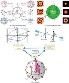
Yuan GAO, Jianping DING, and Huitian WANG
Polarization, as an intrinsic property applying to optical waves, which can specify the geometrical orientation of the oscillation, has always been an important modulated parameter in optical fields. Compared with traditional scalar optical fields, Vector Optical Fields (VOFs) with non-uniform States of Polarization (SoPs) distributions denote that their geometrical orientations of the oscillation dependent on spatial locations are varying. The early research and manipulation on VOFs were limited to a single two-dimensional (2D) plane and mainly focused on the single modal modulation of SoPs. Later, researchers gradually brought to mind that the characteristics of VOFs, such as spatial geometries, polarization distributions, and the law of propagation, were also influenced by their amplitude and phase distributions. So the independent modulations of amplitude and phase based on the achieved polarization modulation caught people’s views and were accomplished after a short time, which means the generation of multimodal VOFs including these three fundamentally modulated degrees of freedom. More importantly, the deep applications related to multimodal VOFs in many realms, such as optical information transmission, manipulation of focal fields, optical micro-manipulation, have attracted researchers’ attention to the significant improvement of modulation efficiencies and the longitudinal extension of multi-dimensional modulation. Specifically, on the one hand, researchers selected the optical elements with high working efficiency and built reformative VOFs’ generators to reduce the unnecessary energy loss in the generation process. On the other hand, they studied the transmission of properties and modulation mechanism along the longitudinal direction for multimodal VOFs. Proposed active methods could modulate the distributions of different parameters, not only include three fundamental parameters amplitude, phase, SoPs but also other complex parameters such as energy flow, angular momentum, and optical singularities in three-dimensional (3D) space. In this review, we present an overview of the recent advances to spatially modulating multimodal 3D VOFs. Firstly, a brief introduction of three representations for a single SoP based on a polarization ellipse, Stokes parameters, and a classical Poincaré sphere respectively, are arranged. After that other three special representations of Cylindrically symmetric SoPs distributions with new types of Poincaré spheres are added. Secondly, we outline several different types of improved extra-cavity methods to generate VOFs, including highly efficient generators of arbitrary VOFs based on phase-only SLMs, compact polarization converters with high conversion efficiency, and sub-wavelength polarization modulators created by metasurfaces. Their advantages and limitations are comparatively demonstrated for readers. Thirdly, we highlight the principle of generating VOFs according to the superposition of two orthogonally polarized basic vectors and consider the applicable conditions of this principle in 3D space. And three relatively effective modulation methods of 3D multimodal VOFs are mentioned. The first utilizes on-axis modulations of non-diffractive Bessel beams to finish the polarization evolution along an optical axis. The second uses Fourier phase-shift principle to achieve independent modulations of polarization modes on multi-planes. The third develops a vector beam-shaping technique in focusing space. These methods are suitable to apply in different optical processes. Finally, the general application situation of VOFs in optical micromanipulation is illustrated to tell readers a great necessity and importance of modulating multimodal VOFs in 3D space.
Jan. 25, 2022Vol. 51 Issue 1 0151101 (2022)
Qian CAO, and Qiwen ZHAN
This paper reviews Spatiotemporal Coupled (STc) optical fields including their theoretical background, the experimental configuration for generating STc optical fields, and the current research status of the newly-discovered Spataiotemporal Optical Vortices (STOV) wavepackets. Firstly, we review the origin and early study of STc optical fields, and introduce the theoretical model for describing STc optical fields. To give an example, we show the spatiotemporal evolution of a STOV wavepacket under normal dispersive, anomalous dispersive, and non-dispersive propagation. Under normal dispersive propagation, the STOV wavepacket maintains its ring-like field structure in the spatiotemporal domain. Under non-dispersive propagation, the STOV wavepacket evolves into a diagonal shape. Under anomalous dispersive propagation, the STOV wavepacket has the polarity reversal during the process. Secondly, we describe the typical experimental setup for generating STc optical fields. Although the experimental configuration for realizing STc optical fields shares almost exact the same experimental setup of a standard 4-f pulse shaper, the generating process is more complicated compared with conventional pulse shaping or beam shaping techniques as it involves a subtle interplay between the dispersion and diffraction effects for the generated STc optical fields. We categorize the operation of a STc optical field generator into three different regimes bythe distance between the exit plane of the generator and the observation plane for the generated STc optical fields: 1) the “far-field regime” where the observation plane is at several Rayleigh range after the generator; 2) the “near-field” regime where the observation plane is within one Rayleigh range; and 3) the “intermediate” regime where the observation plane is placed between “far-field” and “near-field”. For each operation regime, we give an example of the experimentally generated STOV wavepacket, namely, the first experimental realization of STOV wavepackets, STOV lattices, and Bessel STOV wavepackets. Thirdly, we give a detailed review about the state-of-art research status of the newly discovered STOV wavepackets including introducingwhy STOV wavepacket has become an interesting research topic for scientists, the demonstration of the conservation of transverse photonic Orbital Angular Momentum (OAM) proved by a nonlinear Second Harmonic Generation (SHG) experiment, and STOV wavepackets superposed with additional spatial photonic singularities. Compared with conventional vortex beam, the spatiotemporal spiral phase carried by a STOV wavepacket enables the photon within the wavepacket to have a pure transverse OAM, which makes STOV wavepacket an interesting tool in many research fields. Besides STOV wavepackets, other STc optical fields generated by this STc optical field generator setup also feature unique photonic properties such as achieving negative refraction, propagating free of diffraction, and propagation in a controllable group velocity. So far, the pulse shaper based STc optical field generation method has seen great success and received tremendous interests by the research community. Despite the great success already achieved, there are much more need to be studied, understood and developed in STc optical fields. With the unprecedented level of control of the spatiotemporal degree of freedoms of light, spatiotemporally sculptured optical fields will significantly enrich the photonics arsenal for scientistsin broad research fields ranging from quantum optics, nanophotonics, spin-photonics and spintronics, optical information transmission and processing, optical spectroscopy, laser driven particle acceleration, and much more beyond.
Jan. 25, 2022Vol. 51 Issue 1 0151102 (2022)
Xinlei ZHU, Jiayi YU, and Yangjian CAI
Due to its brightness, directionality, and monochromaticity, coherent laser light has been widely used in military defense, medicine, industrial processing, optical communication systems and other fields, playing a vital role in human social progress and economic development. However, with the development of application of laser light, it is found that the one with high coherence will induce some negative effects. Fortunately, it is found that decreasing the coherence can not only keep the original features, but also reduce many negative effects caused by high coherence. Therefore, spatial coherence has gradually become fourth intrinsic property of light that can be optimized for particular tasks, in addition to amplitude, polarization and phase.Laser beams with decreased spatial coherence, called partially coherent beams, and they often have advantages over their coherent counterparts. In the past few decades, researchers only focused on the conventional partially coherent beams, i.e., Gaussian Schell-model beams, and such beams exhibit single and boring propagation property, which cannot meet the increasing demand for laser featrues. Therefore, how to manipulate the propagation features of laser fields to meet the actual demand is particularly important. From the perspective of manipulation of the coherence structures, a new class of light field with prescribed coherence structures can show novel propagation features. Until recently, only a few papers were devoted to partially coherent beams with non-conventional correlations (i.e. non-Gaussian correlated), such as J0-correlated Schell-model beams and vortex-carrying partially coherent beams. Investigations of such beams were limited due to the difficulty in proving that a given function is, in fact, a mathematically valid correlation function.But in 2007, a powerful new method for designing correlation functions of scalar partially coherent beams was introduced by Gori and Santarsiero, followed in 2009 by a more general method for vector partially coherent beams, allowing a wide variety of novel partially coherent beams to be investigated. Among the classes that have been studied since then are multi-Gaussian correlated Schell-model beams, Laguerre-Gaussian correlated Schell-model beams, Hermite-Gaussian Schell-model beams, and optical coherence lattices. Such beams display many extraordinary and potentially beneficial properties, such as flat-topped and ring-shaped intensity profiles in the far field, self-splitting properties, and lattice-like intensity patterns that form on propagation. And they have useful applications in many areas, such as free-space optical communication, particle trapping, image transmission and image encryption.In this review, we first outline the fundamental theories on constructing scaler and vector partially coherent beams with prescribed correlation structures, and then present detailed description of the beams models and their propagation properties of several typical examples. Finally, we review the methods of experimental generation of partially coherent beams with prescribed correlation structures. We hope our review will stimulate further efforts in this area of research.
Jan. 25, 2022Vol. 51 Issue 1 0151103 (2022)
Peng LI, Xinhao FAN, Yu LI, Sheng LIU, Bingyan WEI, and Jianlin ZHAO
Since the invention of the laser in 1960, the relevant basic scientific research, technological development, and engineering application supported by lasers have developed rapidly, making optics enter a new laser era. In last two decades, with the development of laser technology and the growth of its application demand, a series of spatially structured light fields that have elaborate in-plane distributions of amplitude, phase, and polarization have been proposed, such as vector and vortex beams, self-healing and self-accelerating beams, which have shown great potential in solving bottleneck problems such as the diffraction limit of light wave. These spatially structured light fields have been successfully used in realms of super-resolution imaging, particle manipulation, laser micromachining, classical and quantum communication and information restoration, etc. On the other hand, the relevant theories and technologies of light field modulation have further promoted the development of other physical fields. With the in-depth research and wide application of spatially structured light field, scientists gradually focus on the three-dimensional structure control of light field. In this special perspective, the first problem to be solved is the control of light field in the longitudinal dimension, which will provide a more adequate means for the further development of the application of light field in optical micro-manipulation, microscopic imaging, optical processing, angular momentum control, information storage, three-dimensional control of photonic state and so on.In this paper, we give an overview of recent progress on light field intensity and polarization modulation in the longitudinal dimension, and discuss the resulted spatially structured light fields from spatial properties to application potentials. Firstly, we briefly review the on-axis intensity modulation of light field based on the Bessel spectrum control and coherent superposition principles, which enable to create longitudinally modulated fields with discrete and continuous intensity profiles. Next, we describe the light fields with arbitrary propagation trajectories along the longitudinal direction based on two basic theories, i.e., caustic theory and Bessel spectrum mapping theory, which lead to the nontrivial propagation that has with large bending angle in non-paraxial condition. Then, we introduce a special kind of light field with arbitrary trajectory, i.e., the light fields that spirally propagate around the propagating axis, followed by the discussion of generation methods and self-accelerating characteristics of light fields with equidistant spiral, non-equidistant spiral, segmented spiral, and radially structured profiles. We also place particular emphasis on the recent development of polarization conversion during optical beam propagating in free space, and reveal this intriguing phenomenon in the view of spin-orbital angular momentum coupling. Wherein, in contrast to the polarization conversion with intensity profile variation, we introduce a special longitudinal polarization manipulation that exist in scalar and vector beams with non-diffraction intensity profiles. In addition, we trace the joint control of light field intensity and the polarization structure under the tightly focusing condition, which induces a strong longitudinal field component to engineer the longitudinal distribution of light field, and summarize the special three-dimensionally structured light fields constructed from this method.Longitudinally controlling light field not only enriches the spatially structured light field and its relevant theory, e.g., the topologically structured vortex and vector light fields, which have topologies as a new degree of freedom in photonics, it is noteworthy that it also spawns numerous new photonic devices. However, there are still many opportunities and challenges in this rapidly developing research realm. At last, we envision the possible challenges and prospects of longitudinal modulation of light fields, such as how to realize the subtly longitudinal modulation with wavelength-scale variation period, the combined control of multiple parameters along the longitudinal direction, and the construction of novel eigenmodes with three-dimensional spatial correlation, which will stimulate broader and more in-depth theoretical and application exploration.
Jan. 25, 2022Vol. 51 Issue 1 0151104 (2022)
Mingxin LV, Yipeng ZHANG, Jianlang HE, Xiaopeng HU, and Yong ZHANG
The vortex beam laser outputs a high-energy and high-quality vortex beam, which is one typical structured light field. Vortex beam has potential applications in many important fields, such as optical communications, optical manipulation, precision measurement, quantum information, and superresolution imaging. Therefore, how to efficiently generate high quality vortex beam has attracted considerable interests of research in recent years. In this paper, we first briefly introduce the generation principle and main applications of the vortex beam. There are two main ways of generating vortex beams, i.e., active method and passive method. Compared with active method, passive method generally suffers from low conversion efficiency and poor beam quality (especially for high order vortex beams). When a high quality vortex beam is needed, active method is a better choice. The active method generates vortex beams under laser configuration. For example, the high purity vortex beam can be generated by using the mode selection of the laser cavity. At present, the research focus on vortex beam laser is to improve the laser performance and the mode purity of the output vortex beam. In addition, the integration of vortex beam laser, which facilitates various commercial applications, is also a hot topic. Then, we review the recent progress of vortex beam lasers, including solid-state vortex laser, vortex-beam optical parametric oscillator, fiber vortex laser and on-chip integrated vortex lasers. Solid-state vortex laser is one of the most common methods to generate a vortex beam. By properly designing various types of resonators, one can generate the desired laser vortex mode while suppressing the unwanted ones. Taking Laguerre–Gaussian beams as an example, one can use the pump shaping technique to transform the pump beam from a Gaussian beam to a ring shaped intensity profile, which can effectively enhance the gain of the matched Laguerre–Gaussian cavity mode and decrease the gain of other modes. In addition, a tilted etalon can also be used in the resonant cavity to precisely control the gain and loss of different cavity modes. A recent method is to add spatial phase modulation elements (such as spiral phase plate, vortex half-wave plate, and so on) into the cavity. By satisfying the polarization and spatial mode self-reproduction condition of the cavity mode, the output beam can carry a specific spiral phase, i.e., one can obtain a desired vortex laser beam. Interestingly, the use of spatial light modulators and metasurface greatly enriches the types of output spatial light beams. By loading different holograms on the spatial light modulators or properly designing the structures of the metasurfaces, one can get various types of vortex modes, including those with large l and p indices that are difficult to be produced in the previous methods. Along with the foundation of solid state vortex laser, other forms of vortex beam lasers have also been rapidly developed in recent years. Vortex beam parametric oscillator can achieve the output of vortex beam with a tunable wavelength by controlling the phase matching conditions. Compared with the solid state vortex laser, the output wavelength band of vortex beam is greatly expanded. The fiber vortex laser uses the fiber configuration to output vortex beam. The low cost and high stability of the fiber laser can be effectively combined with the vortex beam output for practical applications in high capacity information transmission. This unique characteristic makes fiber vortex laser particularly useful in the field of optical fiber communication. The development of micro/nano fabrication techniques make it possible to integrate vortex lasers on a chip. Finally, we present the prospects of the future development of the vortex beam laser. High conversion efficiency and high mode purity are two critical requirements for high end applications of vortex beam lasers.
Jan. 25, 2022Vol. 51 Issue 1 0151105 (2022)

Bin ZHANG, Lei WANG, Yuechen JIA, and Feng CHEN
Integrated optical circuits play an essential role in the field of optical communication, by which the high-speed processing and transmitting of optical signals can be realized. Optical waveguide, in which the light will be confined into a micron or submicron volume for non-diffraction propagation, is one of the most importantly basic components in integrated optical circuits. The low-loss optical waveguides can be applied to fabricate high-performance photonic devices, e.g., beam splitters, frequency converters, and waveguide lasers. Hence, the fabrication of low-loss optical waveguides is of great significance to many applications in integrated optics and quantum photonics. The optical waveguides in transparent materials can be produced by ion exchange, ion implantation, and Ti-indiffusion. Nevertheless, these waveguides are limited to a 2D planar geometry. The 3D optical waveguides could be fabricated by femtosecond laser direct writing. Femtosecond laser direct writing is a maskless, efficient, and flexible 3D fabrication technique, which has become one of the most widely used techniques for precision machining of materials. The femtosecond laser possesses ultrashort pulse width and extremely high peak intensity, which could lead to the suppression of heat-affected zones and the appearance of nonlinear interactions (e.g., multiphoton absorption, tunneling ionization, and avalanche ionization), respectively. The microscopic objective is often utilized to focus NIR femtosecond laser into transparent materials, resulting in material modifications in focal regions. The material modifications can be classified into two types: Type-I modification and Type-II modification. The refractive index change is positive in the areas of Type-I modification, and the refractive index change is negative in the areas of Type-II modification. By using these two types of modifications, the single-line waveguide, dual-line waveguide, vertical-dual-line waveguide, multi-line waveguide, and depressed-cladding waveguide have been fabricated in transparent materials (e.g., glasses and crystals). In the past 20 years, a variety of photonic devices have been produced with femtosecond-laser-written optical waveguides, such as waveguide arrays, electro-optic modulators, and directional couplers. It can be anticipated that the novel, multi-functional, and high-efficient waveguide-based photonic devices will be created in succession with the in-depth study on laser-matter interactions. Although femtosecond laser direct writing has made a series of achievements in waveguide fabrication, there are still some challenges to rapidly produce low-loss optical waveguide with circular cross-section, due to spherical aberration at the interface caused by refractive index mismatch. In order to improve the waveguide quality and fabrication efficiency, the researchers are dedicated to develop the femtosecond laser writing technique based on light-manipulation. First, slit beam shaping. In this technique, a slit is inserted before the microscopic objective (slit orientation is parallel to laser-scanning direction), by which the aspect ratio of femtosecond-laser-induced track can be greatly reduced. It has been reported that the propagation loss of waveguide written by this processing technique can be reduced to less than 0.5 dB/cm, which is suitable to construct high-performance photonic devices. The slit beam shaping is an effective technique to improve the performance of femtosecond-laser-written waveguides. However, the existence of slit will inevitably result in a lot of loss of femtosecond laser energy, which is a disadvantage of slit beam shaping. Second, astigmatic beam shaping. As for this technique, an astigmatic cylindrical telescope is placed before the microscopic objective to reshape femtosecond laser, by which the waveguide with circular cross-section could be obtained as well. The minimum propagation loss of waveguide fabricated with this processing technique is less than 0.5 dB/cm, which is also applicable to constitute low-loss 3D waveguide configurations. It should be noted that, when fabricating 2D and 3D optical waveguides, the slit beam shaping and astigmatic beam shaping need to adjust slit orientation and cylindrical lens direction, respectively. It is this additional complexity that restricts the further applications of these two beam shaping techniques in integrated photonics. Third, deformable mirror beam shaping. In this technique, a 2D deformable mirror is utilized to reshape the spatial profile of femtosecond laser, by which the propagation loss of waveguide can also be reduced to some extent (~1.5 dB/cm). Fourth, simultaneous spatiotemporal focusing. This technique can strongly reduce nonlinear side effects, and have many potential applications for fabricating low-loss waveguides. However, the waveguide written by this processing technique has not been reported yet. Fifth, spatial light modulator beam shaping. It is a versatile and energy-efficient technique to control energy distribution of laser focus, which is promising to fabricate low-loss and high-quality optical waveguides. This paper, starting from the introduction of five beam shaping techniques, summarizes the latest research advances of waveguides fabricated by shaped femtosecond laser. An outlook is presented including several potential spotlights.
Jan. 25, 2022Vol. 51 Issue 1 0151106 (2022)
Broadband Epsilon-near-zero Metamaterials and Its Application in Optical Field Manipulation(Invited)
Lei SUN, and Guoping WANG
Since the beginning of metamaterial research, epsilon-near-zero metamaterials have long been a research hotspot in the field of electromagnetic metamaterials because of the electromagnetic features granted by their near-zero effective permittivity, making them interesting in both theoretical studies and technical applications. To achieve the near-zero effective permittivity response, in short, the current epsilon-near-zero metamaterial research follows three fundamental theories, the waveguide theory, the band structure theory for photonic crystals, and the effective medium theory. In general, the waveguide theory makes the epsilon-near-zero metamaterials operate as a waveguide at the cut-off frequency, while the band structure theory makes the epsilon-near-zero metamaterials perform as a photonic crystal at the frequency of the Dirac point. On the other hand, the effective medium theory follows another principle of the cancellation of the positive permittivity and the negative permittivity of different components of the epsilon-near-zero metamaterials at a specific frequency. All three theories strongly depend on the electromagnetic properties and the microstructures of the components in the epsilon-near-zero metamaterials, which also limits the near-zero permittivity response frequency. In brief, the single operating frequency and operating mode caused by the inherent limitation of these theories is always a bottleneck preventing further applications of the epsilon-near-zero metamaterials. Therefore, how to break through the limitations, to realize the broadband near-zero permittivity response of metamaterials under multi-stimulation modes, to master its physical principles, and to establish a new theoretical framework are of great significance in theoretical research and application development.In this work, we present a systematic review of our research on broadband epsilon-near-zero metamaterials to address the single operating frequency issue of current epsilon-near-zero metamaterials. In our research, we establish a spectral representation theory for the broadband epsilon-near-zero metamaterials based on the Bergman-Milton spectral representation theory of effective medium theory concerning the characteristics of the effective permittivity spectral representation of typical microstructures of metamaterials and theoretically demonstrate the application of the spectral representation theory in various broadband epsilon-near-zero metamaterials construction. To be specific, the spectral representation theory for the broadband epsilon-near-zero metamaterials firstly abstracts the material and the microstructural properties of the metamaterials into a simple algebra model, in which the broadband near-zero permittivity response can be constructed as will for different probing electromagnetic waves. After that, the spectral representation theory exactly maps the spectral representation of the broadband epsilon-near-zero metamaterials into the physical structures via an analytical inverse algorithm. Through the spectral representation theory, we successfully realize broadband epsilon-near-zero metamaterials with different superlattice configurations in theory, such as the multilayer and the Hashin-Shtrikman structures. Meanwhile, we clearly explain the physical principles of the broadband near-zero permittivity response by numerical simulations. The broadband epsilon-near-zero metamaterials successfully extend the near-zero permittivity property into a wide operating frequency band without changing the near-zero permittivity property. Therefore, they expand the application potential of the epsilon-near-zero metamaterials in broadband optical field manipulation. Through the numerical simulation, we demonstrate several applications of the designed broadband epsilon-near-zero metamaterials, such as the broadband electromagnetic tunneling and focusing, the broadband electromagnetic wave directional emission, and the broadband electromagnetic wavefront modulation. In the end, we wish our achievement can enrich the fundamental theory and application prospects of electromagnetic metamaterials.
Jan. 25, 2022Vol. 51 Issue 1 0151107 (2022)
Runfeng LI, Dashan DONG, and Kebin SHI
The interaction of light and matter has always been a hot issue in research. As a non-intrusive detection method, light can efficiently and non-destructively obtain rich information inside sample. This information either reveals the chemical specificity of the sample and provides a basis for quantitative material composition analysis; or reflects the fine spatial structure of the sample, allowing people to use light as a medium to extract the morphological characteristics of microorganisms and microstructures; or open the time window to observe the sample, using ultra-short light pulses as information carriers to reveal transient dynamics.Spontaneous Raman scattering spectroscopy and imaging technology are important research directions in this field. Since its discovery in 1928, it has gradually become an important research tool in optics. On one hand, Raman scattered photons carry molecular vibration information, which makes up for the insufficient detection ability of infrared spectroscopy at the water absorption window, and provides an important tool for research in the biological and medical fields; on the other hand, as an important label-free detection method, Raman spectroscopy can achieve non-destructive and long-term observation while maintaining sample activity.Since the spontaneous Raman signal requires a long integration time, the imaging speed is greatly restricted when it involves some transient dynamic processes and dynamic observation of living organisms. In order to further improve the intensity of the Raman signal, the Coherent Raman Scattering technology realized by nonlinear optical processes has been developed vigorously. The main methods include Coherent Anti-stokes Raman Scattering and Stimulated Raman Scattering. Compared with spontaneous Raman, coherent Raman greatly improves the signal intensity, shortens the integration time of signal acquisition, and provides new possibilities for high-sensitivity spectroscopy technology and rapid in vivo biological imaging. Since the application of Coherent Raman Scattering, new requirements that have appeared in various chemical, biological, and medical applications are also constantly putting forward new challenges: how to achieve a higher signal-to-noise ratio, greater penetration depth, and faster detection speed, richer spectral information, and stronger resolving power have greatly promoted the rapid development of coherent Raman technology in the past two decades. By combining various optical field engineering methods, such as polarization, chirp, timing, phase and other dimensions of the beam in the non-linear process of coherent Raman, to meet the above challenges, the spectrum and imaging technology can be used in multiple dimensions and have more practical value.This article takes optical field engineering method as the main line, combing through the development and application of CRS spectroscopy and imaging, and mainly includes the principle of the nonlinear process of the coherent Raman method. The main control methods in coherent Raman scattering spectroscopy: incident angle, timing. Finally, there are more abundant control methods in coherent Raman scattering imaging technology: time & chirp, polarization, phase, and spatial frequency engineering.
Jan. 25, 2022Vol. 51 Issue 1 0151108 (2022)
Yudong YANG, and Zhiyi WEI
Ultrashort laser pulses are powerful and important tools for scientific researches in many areas in that they allow studying ultrafast dynamics in materials with extreme time resolution. Different experiments across different research fields ask for laser pulses with very different characteristics. Ultrafast laser pulse shaping, where the amplitude, phase or polarization of laser pulses are modulated to fulfill various requirements of different experiments, is widely used. On the other hand, the pure quest of the technology development and the desires for studying even faster dynamics in materials jointly motivate the development of ultrafast laser technology. The record of the shortest pulse duration was continuously renewed. Eventually, ultrafast lasers step into the few cycle regime thanks to the introduction of Ti:Sapphire lasers. When the pulse duration approaches the oscillation period of the laser carrier wave, the differences between few cycle pulses and longer pulses emerge. One of the most notable differences is that even for two few cycle pulses with identical envelopes, the electric fields underneath can be utterly different. Hence, full control over few cycle pulses requires direct control over the electric field, which implies the technological leap from laser pulse shaping to sub-cycle laser field shaping. Sub-cycle laser field shaping technology not only enables full control over laser pulses, but also makes possible direct manipulation of strong-field physics process via tailored optical waveforms, which fundamentally enhances the toolbox for controlling light and matter interaction.Preliminary laser field shaping can be achieved via the Carrier Envelope Phase (CEP) of laser pulses, which is sufficient to significantly affect the electric field and alter the outcomes of light and matter interactions. Therefore, CEP stabilization is crucial for laser field shaping. Currently, CEP locking methods can be categorized into active stabilization and passive stabilization. Active CEP stabilization requires feedback loops which lock the CEP mostly by tuning the inter-cavity group velocity dispersion. In contrast, the passive CEP stabilization exploits the phase relation between different beams in nonlinear optics process, where the idler beam of OPA/DFG is naturally CEP stabilized if the signal beam and the pump beam shares identical CEP fluctuation. Additionally, controlling the spectral phase precisely further enhances the shaping capability that the electric field can be shaped to deviate notably from sinusoidal oscillation. Complete characterization of such few-cycle/single-cycle pulses is indispensable for utilizing them in experiments. Typical ultrashort pulse characterization methods measure the pulse envelopes but the exact shape of the electric fields. New methods which measure the electric field have to be developed. The field-sensitive methods are usually based on high harmonic generation, either by exploiting the process itself or by employing the XUV radiation from HHG.Laser field shaping targets extending the capability of direct electric field control in radio frequency to optical frequency. Customizing optical waveforms builds on the generation of extremely broadband spectrum and precise control of the spectral phase. Since laser pulses with broad bandwidth correspond to pulses which are temporally compressible to very short duration, sub-cycle laser field shaping and sub-cycle laser pulse generation share common technological ground. However, generating spectrum experimentally with bandwidth supporting sub-cycle laser pulses with a single light source is, if not impossible, extremely difficult. On the other hand, coherent combination, or synthesis, of several few-cycle pulses of different colors is the enabling technology for extremely broadband spectrum and intense sub-cycle laser pulses. Different approaches have been proposed along the development of optical waveform synthesis. The optical waveform synthesizer based on noble gas filled hollow-core fibers is one of the most successful attempts, which leads to fruitful results. However, the HCF approach has its own limits which are, e.g. the pulse energy and the bandwidth. To overcome such limits, OP(CP)As are introduced for the waveform synthesis. After conceptual demonstration with small OPAs, the signal beam, the idler beam and even the pump beam of more powerful OP(CP)As are employed for coherent synthesis, which takes advantage of the fact that the beams are inherently synchronized. The full potential of a parametric waveform synthesizer is however yet to explore. Hence, a waveform synthesizer consists of several different OP(CP)As was built, which outputs millijoule level sub-cycle pulses and the waveform can be varied by tuning the synthesis parameters. With the intense sub-cycle pulses, isolated attosecond pulses are directly generated without the assistance of additional gating methods. Moreover, tunable isolated attosecond pulses are conveniently delivered via varying the synthesis parameters. In the meantime, simulations are performed to illustrate the shaping of the generated attosecond pulses by tailored waveforms.
Jan. 25, 2022Vol. 51 Issue 1 0151109 (2022)
Dina MA, Hua CHENG, Jianguo TIAN, and Shuqi CHEN
In the past three decades, artificial photonics devices have made remarkable achievements in the fields of super-resolution, biosensing and optical communication. The designs of traditional photonics devices are usually realized by analyzing physical models and establishing numerical simulation methods. However, the structural design based on the numerical simulation method largely depends on the empirical model, and a large number of parameter combinations need to be calculated in the process of structural optimization, so it can only get suboptimal results in a limited parameter space. With the continuous improvement of computer computing capability and the enrichment of computer algorithms, the inverse design of photonics devices can effectively solve the above obstacles. The inverse design method can not only find the optimal structure distribution in a broader parameter space, but also design irregular structures that cannot be directly designed by human brain, which makes the performance of inverse designed photonics devices closer to the limit. This review first introduces the three common methods of photonic device inverse design and then introduces several important applications based on inverse design methods in detail. Common inverse design methods can be divided into gradient descent algorithm and genetic algorithm. Gradient descent algorithm uses gradient information to guide the optimization of structure. Topology optimization is a commonly used algorithm in gradient descent algorithm, which can optimize the material distribution in a given design area according to the given objective function and constraint function. The gradient of objective function in topology optimization is usually calculated by adjoint method. Genetic algorithm looks for the global optimal value by simulating the evolution process of “survival of the fittest”. The algorithm has four main steps: initial population guess, crossover, mutation and selection. By iterating the above four steps for a certain number of times, the whole population can evolve in the desired direction. The deep learning model can effectively extract features from a large amount of data and has been proved to characterize the physical relationship between photonic structures and their optical properties. The trained deep learning model can replace the electromagnetic simulation process and greatly reduce the design time of photonics devices. Based on the above characteristics, these algorithms have been successfully used in the design of photonic crystal, metagrating, metasurface and other optical devices. However, inverse design methods are not omnipotent. They have different limitations. For example, gradient descent method usually converges to the local optimal value, so it needs a better initial starting point. Genetic algorithm has a large amount of calculation and is sensitive to parameter setting. Deep learning needs data sets, and the performance of the network is affected by super parameter setting. Therefore, when selecting the inverse design method, it is necessary to evaluate the calculation time and optimization dimension of the physical model. Intelligent algorithm combines nano photonics with computational science, and provides researchers with an efficient new design method. In the future, the difficulty of optical field manipulation can be simplified by intelligent inverse design methods, so as to achieve the purpose of designing high-performance optical devices from the demand.
Jan. 25, 2022Vol. 51 Issue 1 0151110 (2022)
Zhiwei GUO, Haitao JIANG, and Hong CHEN
Manipulating the isofrequency curves of materials can effectively improve the interaction between light and matter. In recent years, based on the hyperbolic metamaterials, it has been widely proved that the topological phase transition from closed circle to open hyperbola will strongly affect the light transmission and radiation. In this review, a new type of anisotropic metamaterials, Linear-Crossing Metamaterials (LCMMs), which exist in hyperbolic topological transition is introduced. Because the signs of the in-plane permeabilities are opposite and the permittivity tends to zero, an LCMM may simultaneously possess the characteristics of an hyperbolic medium and a zero-index medium. On one hand, LCMMs support high-k modes just like hyperbolic medium because of the open iso-frequency contours. On the other hand, the linear dispersion relationship of the LCMMs ensures that the group velocity is perpendicular to the phase velocity, which leads to the zero phase accumulation along the propagation path just as in a zero-index medium. In addtion, LCMMs can have many unique properties. For example, considering that the signs of the in-plane permeability can also be tuned, two kinds of LCMMs with positive and negative refractions will be realized. Moreover, the refraction angle of incident light will be locked in two fixed directions that are independent of the incident angles. For a vertical incident beam incident on the LCMM, it will split into two beams just as does the valley-dependent propagation in photonic crystals. Due to the fact that the refracted light is locked in the two fixed directions, the propagation of light will not be affected when we put a defect inside the structure so long as it is not placed in the path of refraction. This property can be utilized for a partial cloaking effect that is robust to the presence of defects. LCMMs can also be used to realize the non-diffraction Bessel beam possessing unique self-healing properties. By mean of directional propagation and negative refraction, a point source instead of the plane wave can realize the Bessel beam through a planar LCMM. In a word, LCMM is a very interesting research topic and a wide range of potential applications based on LCMMs need to be explored. Especially, the realization, novel physical properties and important applications of linear-crossing metamaterials are summarized. Finally, the development of the research on linear-crossing metamaterials is prospected.
Jan. 25, 2022Vol. 51 Issue 1 0151111 (2022)
Licheng LUO, Hengyi LI, Manzhu KE, and Zhengyou LIU
Acoustic communication has been widely used underwater due to its relatively low loss. However, acoustic wave doesn’t have the physical properties of spin and polarization like electromagnetic wave, which makes it impossible to broaden the channel capacity by these ways. Meanwhile, orbital angular momentum provides a new option for acoustic communication as a new degree of freedom independent from time and frequency. In this case, vortex beams, which carry the orbital angular momentum, are attracting great attention for their potential application of making acoustic waves transfer more information at the same frequency. As one kind of the vortex beams, Bessel beams have the characteristics of highly-localized energy and non-diffraction. In this manuscript, an artificial structure plate with hollow Archimedes spiral grids has been designed to manipulate the phase of the output wave with different incident acoustic wave. The spacing between the spiral grid is equal to the wavelength corresponding to the fundamental frequency. The flexible manipulation of the acoustic Bessel beam’s phase and topological order assisted by this plate have been studied theoretically and numerically. Based on Huygens principle, the distribution of output acoustic field produced by the incident plane wave or Bessel beam which travel through the plate from the front or the back side is derived. The result shows that when the plane wave transmits the plate from the opposite directions, the outgoing Bessel beam with opposite topological order can be obtained separately; when Bessel beam transmits the plate from the opposite direction, the outgoing Bessel beam with ascending or reduced order can be obtained. When the working frequency increases to a multiple of the fundamental frequency corresponding to the artificial structure plate, the higher multiple phase and topological order manipulation for the incident wave can be obtained. Similar result can also be derived by increasing the spacing between the spiral grid to a multiple of the wavelength. The result of numerical simulation is consistent with the theoretical derivation. And the theory also applies to high-order Bessel beam. Therefore, acoustic Bessel beam with arbitrary topological order can be obtained by this way. This proposed method has possible potential to promote the application of orbital angular momentum in information transfer and information encoding and decoding.
Jan. 25, 2022Vol. 51 Issue 1 0151112 (2022)
Chunlei SHANG, Shi WANG, Chengzhen LU, Chunhao LIANG, Yuanmei GAO, Yangjian CAI, and Zengrun WEN
Doped LiNbO3 crystal is one kind of photorefractive mediums which are used for optical storage. When light passes through LiNbO3 crystal, it will cause local refractive index change and form noise grating. The noise grating diffracts the incident light, transferring part of the light energy to the scattered light, namely, light-induced scattering. In recent years, the modulation instability, generation process and energy transfer efficiency of light scattering in LiNbO3 crystals have been widely studied. Since a single component of linearly polarized light is used for the incident, no variation of the polarization state of the outgoing light is observed. However, considering the difference of energy transmission efficiency between o-light and e-light, it is reasonable to guess that the polarization state of the outgoing light may change when another light is incident. According to our investigation, there is no research in this field. In this work, the variation of the polarization state of LiNbO3:Fe crystal during the light-induced scattering process is reported. The circularly polarized light is focused into a thin light sheet and irradiated on the crystal with the c-axis along the vertical direction. The light scattering phenomenon at different incident angles is studied. In the tens of minutes from the generation of the scattered light to the steady state, the scattered light mainly grows in the direction parallel to the c-axis, and there is also a component in the direction parallel to the light sheet. The growth rate of scattered light decreases with the increase of the incident angle. Further observation manifests that the circularly polarized light becomes ordinary elliptically polarized light after passing through the crystal, and the ellipticity varies with the incident angle. Combined with the noise grating formed in the crystal, the scattering model of circularly polarized light is established, and the reason and mechanism of polarization state change are analyzed through calculation. Qualitative analysis shows that the ellipticity of scattered light is related to the transmission coefficient τ and azimuth angle, and the left-handed or right-handed polarization state is also related to the phase difference δ between o-light and e-light. This discovery proposes a method to generate elliptically polarized light using the light-induced light-scattering properties of photorefractive crystals, which can be applied to optical storage and photonic lattice based on photorefractive materials.
Jan. 25, 2022Vol. 51 Issue 1 0151113 (2022)
Fuyuan GUO, Lianhuang LI, and Hua ZHENG
In the optical system, the conjugate transformation of the light field between object and its image is a common transformation. Based on the paraxial approximation and the Fresnel diffraction theory, the relation of light field between the object plane and its conjugate image plane of lens is presented in the book of Introduction of Fourier Optics. It is consistent with the scale transformation of the geometric optics prediction. The sine condition is a requirement for lens which carries out a perfect image for the object with vertical axis facet in an optical system. It was demonstrated by Fermat's principle in the field of geometrical optics, but it could not be explained by the classical diffraction integral formulae in the non-paraxial field.As the law of conservation of radiant energy in the traveling wave field was underappreciated in the classical diffraction theory, the classical diffraction integral formulae have limitations. As the Huygens' principle and the law of conservation of radiation energy in traveling wave field were engaged for analyzing the diffraction process of the non-paraxial light field in the cylindrical coordinate system, it was presented that the rationality of the normalized inclination factor was expressed by the square root of the cosine of the inclination angle in the side of diffraction source for analyzing the far field characteristics what diffracted from small light fields with flat wave front, and it was presented that the rationality of the normalized inclination factor was expressed by the square root of the cosine of the inclination angle in the observation side for analyzing the characteristics of the light field in the focal plane what diffracted from convergent hemispherical wave front also.Based on the normalized inclination factor expressed by the square root of the cosine of inclination angle, the non-paraxial integral formulas for analyzing the far-field characteristics of the diffraction source with the symmetric small flat wave front and the focal plane field characteristics of the diffraction source with the symmetric convergent wave front are suggested in the rectangular coordinate system respectively. As the light field of the diffraction source is a symmetric traveling wave field, and the Parseval's theorem and the calculation formula of the total power of the light field on the reference surface are employed, the total power of the light field on the observation reference surface which was expressed by the new normalized inclination factor equal to the total power of the light field on the diffraction source reference. It satisfies the law of conservation of energy. So the new normalized inclination factor is reasonable.As the Huygens' principle is engaged for analyzing the diffraction process of the symmetric traveling wave field, both the diffraction source reference surface and the observation reference surface coincide with the light wave fronts. The diffraction source reference surface is a small flat wave front, and the observation reference surface is a hemispherical wave front for analyzing the far field characteristics what diffracted from small light fields with a flat wave front. The diffraction source reference surface is a hemispherical wave front, and the observation reference surface is a small flat wave front for analyzing the characteristics of the light field in the focal plane what diffracted from the convergent hemispherical wave front. These two diffraction processes are the process of exchanging the diffraction source reference surface and the observation reference surface. If the diffraction source reference surface and the observation reference surface were reciprocated, the expression function of the traveling wave field of symmetric diffraction source and the expression function of the traveling wave field of observation surface in two diffraction integral formulae are reciprocated, and the functions of two inclination factors in two diffraction integral formulae are reciprocated also. Then, the reciprocity between the non-paraxial diffraction integral formula used to calculate the far field distribution of light wave what diffracted from symmetric small traveling wave field with a flat wave and the non-paraxial diffraction integral formula used to calculate the light field distribution of focal plane what diffracted from symmetric traveling wave field hemispherical wave front is clarified.As the normalized inclination factor of diffraction source side expressed by the square root of the cosine of inclination angle of diffraction source side and the normalized inclination factor of observation side expressed by the square root of the cosine of inclination angle of observation side are engaged, and the apodization function of the lens on the normal of light wave front is taken into consideration. The scale transformation characteristic of traveling wave fields with flat wavefront between the object-image conjugate planes of the lens which satisfied the sine condition is verified, and the applicable conditions of the relationship of scale transformation are expounded.
Jan. 25, 2022Vol. 51 Issue 1 0151114 (2022)
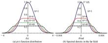
Weiwei XIAO, Han ZHANG, Xinying ZHAO, Yang MA, and Xiaoyan PANG
A vortex beam is a kind of beam with a spiral phase surface, and in the beam center there is a phase singularity, thus the intensity is zero. Vortex beams can theoretically carry Orbital Angular Momentum (OAM) with any mode, and the vortex beams of different OAM modes are orthogonal to each other. Because of these special properties, vortex beams have received extensive attention from researchers and have been widely applied in the fields of wireless communication, optical tweezers and microscopes. However, the most researches on vortex beams concentrated on the canonical ones, whose phase gradient is constant along a circular path around the vortex center. The canonical vortices can be simply expressed as Aein? (A is the amplitude of field, ? is azimuthal angle and n reperents the topological charge of the vortex), which in many circumstances are usually called ‘optical vortices’ for short. The ‘noncanonical’ means that the phase gradient of the vortex is not constant, while the topological charge is also the same as it in its ‘canonical’ counterpart. Actually, the noncanonical vortices were studied by several scientists, but only the forms of the noncanonical vortices satisfying the paraxial wave equation were taken into consideration. There, the ‘noncanonical’ vortices were also called ‘anisotropic’ vortices, since not only the phase but also the amplitude of such vortices was spatially anisotropic. The researches on the noncanonical vortex wave are mainly concentrated in the scalar field, such as the study of the trajectory of noncanonical vortices in free space, the phase singularity and energy flux of noncanonical vortex dipole Airy beams. Recently, PANG Xiaoyan et al proposed a new type of noncanonical vortex, named X-type (noncanonical) vortex. This vortex inherits and develops the conventional noncanonical vortex, i.e., it no longer has a constant phase gradient around the beam center, while the intensity keeps invariant azimuthally. In this article, the X-type (noncanonical) vortex with left-handed circular /right-handed circular polarization is studied in a tightly focusing system. In this tightly focused (vectorial) field, the Spin-Orbit momentum Interactions (SOIs) occur, and as we know that the SOIs play crucial roles in many circumstances and studying the optical behaviors involving SOIs continuous to attract a lot of attention. As it is shown in this article under the SOIs the X-type vortex shows interesting propagation properties. By applying Richards-Wolf diffraction theory, this three-dimensional (3D) focused field is expressed and analyzed. Here we mainly focus on the intensity distribution of this 3D field, and the behaviors of the total intensity on the focal plane and on the transverse planes along the beam propagation are discussed. The topological charge of the X-type vortex in this article is chosen as 1, the fundamental charge, and 2 the higher order charge. For the much higher orders, such as 3 or 4, the analyses of these fields can follow the same method that given in this article. The comparison between the behaviors of the field intensity for the incident field with left-handed circular polarization and the right-handed circular polarization are made, which also is discussed with the result in previous study for the linear polarization. It is found that the total intensity of the field shows the transverse focal shift in the focal plane and the rotation behavior along the propagation, and these properties of the intensity are distinguishing from those in the field without SOIs. The main conclusions are: First, the anisotropy parameter c of the X-type vortex is the main reason for generation of the transverse focal shift and the intensity rotation of the X-type vortex, and the semiaperture angle α, polarization state and the topological charge all have effects on manipulation of the intensity distribution. Second, both the rotation direction and the total rotation angle of the intensity pattern of the focused field are independent of the polarization state of the incident field. Third, the difference between the intensity distributions of the strong field for the incident wave with the left-handed circular polarization and the right-handed circular polarization is a result of the SOIs, and the same behavior for these two cases is that they have the same switch value c=1 on the focal plane, which is different from the switch value of the linear polarization. In the case of linear polarization (without the SOIs) the switch value of the anisotropy parameter is always smaller than or equal to 1, i.e., it changes with the system parameters. Fourth, for the second-order of the X-type vortex, although the transverse focal shift and the intensity rotation of the beams are different for the left-handed and right-handed circular polarizations, the distribution of the main vortices and the rotation behavior in two cases are the same. Our work may give a new way to explore the noncanonical vortices and will supply an additional method for tailoring 3D optical fields, which may have potential applications in optical tweezers and other fields.
Jan. 25, 2022Vol. 51 Issue 1 0151115 (2022)
Yakun WANG, Yuping TAI, and Xinzhong LI
As a composite optical field, Airy vortex beam possessing transverse and longitudinal superimposed modes has abundant intensity and phase distributions. However, the composite optical field is limited to the specific propagation direction and complex modulation of the propagation trajectory. To address these issues, based on the multicoordinate transformations, one-dimensional Airy beam, two-dimensional Airy beam and Airy vortex beam have been transformed in different coordinate systems, respectively. We have realized the orientation modulation of the two lobes of Airy beam and the embedded optical vortex in the range of 0-2π, independently. We have studied the propagation properties in the propagation distances of 0, 2, 6, and 10 cm in the case of the obtuse and acute angles between two lobes of the Airy beam and the Airy vortex beam with orthogonal lobes, respectively. The results of experiments and numerical simulations show that the generated optical field can propagate along arbitrarily appointed parabolic trajectories and directions in free space. In addition, a method for measuring topological charge is proposed by adding the shift factor d when the directions of the lobes are opposite. This proposed method enables in situ determination of the embedded optical vortexes' topological charge without the need for additional optical elements, and it is immune to environmental vibration and parasitic interference. Our results promote the applications of Airy vortex beam in particle manipulation and optical cleaning and provide an alternative scheme for the modulation of composite optical field.Measurement of the topological charge and the intensity profiles at different propagation distance via the experimental setup.
Jan. 25, 2022Vol. 51 Issue 1 0151116 (2022)
Tong XIAO, Changhui TIAN, Cuilian XU, and Zhiqiang GAO
In recent years, metamaterials have attracted great attention in stealth technology. As a special two-dimensional metamaterial, hypersurface is more suitable for the design of infrared radar compatible stealth structures. Based on optically transparent materials Indium Tin Oxide (ITO), Polyethylene Terephthalate (PET) and Polymethyl Methacrylate (PMMA), an optically transparent infrared radar compatible stealth composite metasurface is realized by using the idea of integrated design of infrared low emission layer and radar absorbing layer. The structure consists of three parts: functional layer, dielectric layer, and reflective back plate, with a total thickness of only 1.17 mm. By etching the ITO pattern on the surface of the functional layer and optimizing the pattern size of the pattern, the broadband absorption higher than 90% in the frequency range of 15.9~35.1 GHz in the microwave band is realized. At the same time, the infrared emissivity is reduced by increasing the ITO duty cycle on the surface of the functional layer, and the infrared emissivity on the surface of the structure is controlled at 0.25. Based on the analysis of the surface current of the material, the mechanism of super surface absorbing wave is expounded, and the influence of different patches on the absorbing wave ability is analyzed. Through the analysis of surface current, it is found that almost only the small square patch in the middle and four large square patches around form the resonant structure, while the four rectangular patches and the peripheral square patches make little contribution to the resonant consumption. When the middle rectangular patch does not exist, the bandwidth absorbed by 90% of the high frequency part can be increased by nearly 5 GHz, but it also means that the proportion of ITO on the surface of the structure is reduced, which affects the infrared emissivity of the whole structure. Through simulation experiments, the changes of the absorbing capacity of the designed structure at different incident angles are discussed. For TE mode, the structure can maintain high absorptivity when the incident angle is less than 30°. With the further increase of the angle, the absorptivity of the low-frequency part decreases more. For TM mode, the absorptivity of the structure is only about 0.8 when the incident angle is small. With the increase of the incident angle to 35°, the structure can maintain 90% absorptivity in the range of 20.1~35.0 GHz. It shows that the absorbing ability of the structure at large incident angle in TM mode is stronger than that in TE mode. In order to further verify the simulation results, the conductive ITO film deposited on the optically transparent PET substrate was etched into the designed structure by laser etching technology, and the experimental sample was processed, the sample size was 360 mm×360 mm. The microwave absorption capacity, infrared emissivity and visible light transmittance of the sample were measured respectively. The microwave absorption performance is tested in the microwave darkroom. The measurement system is composed of Agilent N5224a network analyzer and three pairs of broadband horn antennas. During the measurement, the metal base plate with the same size is selected for normalization, and then the reflectivity is measured. After calculation, the absorption curve is obtained. Considering the square resistance and size error of ITO in sample processing, it is considered that the experimental results are basically consistent with the simulation results. The optical transparency performance is measured by ultraviolet visible spectrophotometer (model: uv-3600 plus). After calculation, the average visible light transmittance of the overall structure is about 0.704. The results effectively show that the designed integrated infrared radar compatible stealth composite hypersurface has good optical transparency performance in the visible band. For the infrared emissivity of the designed structure, Tss-5x infrared emissivity tester (spectral response range: 2~22 μm) and FTIR spectrometer are used to measure the emissivity of the sample. ITO film of 6.0 Ω/sq, pet substrate and material samples etched with ITO pattern are measured respectively. In order to ensure the effectiveness of the measured data, each material is measured at five different positions, and the obtained infrared emissivity is 0.246, which is very close to the average infrared emissivity of the designed material sample obtained by direct measurement of 0.248. The infrared emissivity of the sample with the designed structure in the range of 3.0~14.0 μm is measured by FTIR spectrometer, which is about 0.25, which is close to the theoretical calculation value and the measurement value obtained by Tss-5x infrared emissivity tester. It can be considered that the designed structure has better infrared stealth ability. The structure has thin thickness, good broadband radar absorption performance, low infrared emissivity and visible light transparency.
Jan. 25, 2022Vol. 51 Issue 1 0151117 (2022)
Zhihua FAN, Yufei WU, Xiaoyu MA, and Shaolin ZHOU
In priciple, metasurfaces for phase regulation based on the generalized Snell’s law enable arbitrary wavefront or spatial phase tuning via ultrathin interface with deep subwavelength thickness. Specifically, such ultrathin metasurfaces are essentially composed of anisotropic meta-elements that are eleborately arranged to achieve phase modulations pixelwisely in a subwavelength-level local manner in a full range covering [0 2π]. However, most current metasurfaces lack of the flexibility of active tuning due to their post-factication passive nature. In this situtations, the ultracompact reconfigurable devices with high-level of integration become highly desirable for a few applications such as the active photonic, optoelectronic integration and so on. Therefore, this paper aims to combine the actively tunable property of newly emerging phase change materials with the framework of metasurfaces with the functions of phase tuning based on the generalized Snell's law. As proof of concept, the far-field switchable holographic imaging is reasonably demonstrated acting as one type of meta-switch for certain scenarios of controllable hologram generation. In detail, the phase change material of germanium antimony telluride (Ge2Sb2Te5, “GST” in short) alloy is integrated into the meta-atom design for the essential switchable control. For the amorphous-GST integrated device incident by the circularly polarized wave, the predefined anisotropic meta-atoms can achieve broadband (1.55~2.8 μm) geometrical phase modulation with the polarization conversion ratio (PCR) up to ~80%, producing the near-field holographic phase distribution for the far-field holographic imaging, i.e. the “on” state for our device. However, upon the phase change of GST to its crystalline state, the PCR of meta-atoms is minimized and the holographic phase and image reconstruction are then switched off. As a result, the phase-type photonic switch proposed in this paper have great potentials in active photonic and optoelectronic integration such as the spatial light modulation, wavefront engineering, holographic imaging.
Jan. 25, 2022Vol. 51 Issue 1 0151118 (2022)
Dongmei ZHOU, Aihuan WANG, Cuiran LI, Xiaosuo WU, and Baowan YAN
In recent years, the silicon-on-insulator platform has attracted much interest in implementing integrated optical circuits. Due to the high refractive index contrast between the waveguide and cladding, the silicon-on-insulator waveguide has a strong light confinement ability, which helps the device to achieve a compact structure size and large-scale integration. However, this high refractive index contrast causes silicon nanophotonic devices to have high polarization sensitivity so that TE and TM modes have different propagation characteristics in an identical silicon-on-insulator waveguide, which may disrupt the optical signals in optical interconnections and quantum communications. To tackle this problem, one solution is using a polarization beam splitter to polarize the TM mode and TE mode light. Considering future ultra-dense photonic integrated circuits, a compact PBS with high performance is desired. Therefore, the hybrid plasma waveguide is introduced into the design of the polarization beam splitter. The hybrid plasmonic waveguide consists of a high refractive index dielectric layer (e.g., Si), a metal cap (e.g., Ag), and a thin low-index material layer (e.g., SiO2) between the Si layer and the metal layer. Compared with the traditional dielectric waveguide, it has a significant birefringence effect, which can maintain the performance of the device and further reduce the size of the device.In this paper, we propose and optimize a novel hybrid plasmonic polarization beam splitter utilizing asymmetrical directional coupling between the dielectric waveguides and a hybrid plasmonic waveguide on the silicon-on-insulator platform, which is ultracompact, and low-loss. Employing phase-matching conditions and super-mode theory, this polarization beam splitter is elaborately designed. The device is a three-waveguide asymmetric directional coupler. The middle hybrid plasmonic waveguide, which has a dielectric-loaded structure to enhance the refractive index contrast, is defined as the input waveguide. And different silicon-based waveguides on both sides are used to couple and separate TE and TM modes. Compared with the traditional polarization beam splitter based on the directional coupler composed of the same waveguide, this device facilitates two different types of waveguides to enhance the structural birefringence, which provides the device with an ultra-short coupling length and high extinction ratio. In addition, the dependence of TE and TM modes on the middle waveguide is also weakened.In this design of the device, it is necessary to ensure that the input waveguide and the TM coupling waveguide are phase-matched in the TM mode, but not phase-matched in the TE mode. In the case of the TE coupling waveguide, the principle of phase matching for TE mode is similar. The finite element method is used to calculate the mode field distribution and effective refractive index of silicon waveguides and a hybrid plasmonic waveguide, and then determine the size of each waveguide according to the phase matching conditions, which provides a basis for device modeling and simulation analysis. And the 3D finite difference time domain method is used to study the mode characteristics and optimize the structure of the polarization beam splitter to obtain better performance parameters. The experimental results show that the coupling lengths for TE and TM modes are 4.2 μm and 4.6 μm, respectively, and the polarization conversion efficiency of the modes can reach 94.7% and 95.5%, respectively. It can be seen from the light propagation of the polarization beam splitter that when the TE polarization mode is launched from the input side of the hybrid plasmonic waveguide, it is gradually coupled to the TE coupling port in the coupling region, with scarcely any modes mixing. Similarly, when the TM polarization mode is input into the hybrid plasmonic waveguide, it is finally coupled to the TM coupling port. For the TE mode, the polarization extinction ratio value is -38.9 dB and the insertion loss is -0.5 dB at the wavelength of 1.55 μm. For the wavelength range from 1.48 μm to 1.62 μm, the insertion loss of the TE mode is less than 0.92 dB, and the polarization extinction ratio is lower than -28.3 dB. For the TM mode, the polarization extinction ratio is -34.7dB, and the insertion loss is 0.45 dB at the wavelength of 1.55 μm. In the 140 nm wavelength range centered at 1.55 μm, the insertion loss of the TM mode is less than 0.89 dB, and the polarization extinction ratio is lower than -34.6 dB. The above experimental results mean that the performance of the polarization beam splitter is not sensitive to the wavelength. In addition, the influence of fabrication tolerance of waveguide in polarization beam splitter on device performance is also studied. Within the fabrication tolerance range of waveguides, the insertion loss of the mode is less than 2.8 dB, and the extinction ratio is lower than -22.5 dB. The results show that the device has high fabrication tolerances. In summary, the polarization beam splitter designed in this paper has a high extinction ratio, low insertion loss, and the coupling length is only 4.6 μm. It has great potential application value in the ultra-small silicon-based optical integrated circuits in the future.
Jan. 25, 2022Vol. 51 Issue 1 0151119 (2022)
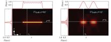
Ao TANG, Bin LAN, and Feng SHEN
High-power vortex lasers have good application prospects in optical processing and other fields. At present, most methods of generating vortex beams outside the cavity use phase-type devices, such as spiral phase plates and spatial light modulators, and these methods can not withstand high-power laser. The spiral mirrors can be used to generate high-power, but they can not flexibly modulate the vortex beam modes. Thus, the technology of generating mode-tunable high-power vortex beams is still a problem to be solve. In this paper, A method based on the Deformable Mirror (DM) with continuous surface to generate vortex beams is proposed. According to the helical symmetry phase of the vortex beam, the arrangement style of the actuators is designed as a ring, and by generating annular spiral wavefront to solve the DM can not fit singularity. Meanwhile, the annular spiral wavefront has the effect of suppressing side lobes. By comparing the mode purity of the annular spiral wavefront generating via the DM with different numbers drivers, the arrangement of driver arrays is determined, five rings and the number of drives in each ring from the inside to the outside is 15, 20, 25, 30, 35.Since the DM with continuous surface can not produce the ideal spiral wavefront, and the constant size beam used in simulation can not achieve the best effect of sidelobe suppression for the vortex beam with any mode. Therefore, there are high-frequency noise and high-order diffraction sidelobes in the vortex optical field generated by the DM designed. Hence, we add 4f filtering system to the optical path to remove they, and the expression of the radius of the main lobe of the vortex beam on the focal plane is derived as the radius of the filter hole. Finally, The sidelobe-free vortex beams with the topological charge equal to -5~5 are generated by simulation, whose amplitude distribution is a destructive ring, and the phase is quite close to the ideal spiral phase, furthermore, the mode purity is closed to 1 after filtering.The above results prove that the DM with continuous surface combined with the filter system can be used to generate a vortex beam with high mode purity. Moreover, the DM with continuous surface can flexibly generate different wavefront, and can withstand high-power laser, thus, this method has a good application prospect for generating high-power vortex beams with adjustable mode.
Jan. 25, 2022Vol. 51 Issue 1 0151120 (2022)
Yimunan XIE, Xiaoping JIANG, Sumei ZHOU, and Zhe YUAN
The plane microlens array is a plane array that is buried under the surface of the flat glass substrate,which consists of several microlens elements with uniform geometric dimensions and a three-dimensional gradient of refractive index according to a certain rule. There are many methods for making GRIN planar microlens arrays, including hot embossing technology, ion beam etching, the melted photoresist method, and so on. Each of these methods has certain advantages and limitations. The hot embossing technology has high pattern reproduction accuracy, but the demolding process is complicated. Using ion beam etching to fabricate microlens has good surface microstructure, but the production cost is high and production efficiency is low. The melted photoresist method has a simple manufacturing process, but the planar microlens array made by this method has poor thermal stability and is prone to aging. The fabrication process of GRIN planar microlens array using ion-exchanging method is relatively simple. The size of the lens element fabricated by ion-exchanging method can be less than 10 μm, the focal length can be less than 0.1 mm, and the thickness can be less than 0.1 mm. Moreover, the array structure and imaging uniformity are good. It has been widely used in artificial intelligence, portable equipment, integrated imaging, three-dimensional imaging, beam homogenization, beam shaping and other fields that require small-sized array optical elements. In this paper, circular aperture gradient index plane microlens arrays with different diameters are fabricated by ion-exchange technology and photolithography. By sampling in 6 time intervals during the ion-exchange process, the ion-exchanging depth and width of microlenses with different aperture sizes, the focal length, distortion and numerical aperture of lens elements were measured. The ratio of ion-exchange width to depth decreases with the increase of ion-exchange time, and the average diffusion rate of ions in the z-direction and r-direction gradually decreases. Moreover, that decreases faster for the flat microlens array with small opening diameter. As the ion-exchanging time increases, the focal lengths of the microlens arrays with two apertures gradually become shorter, and the focal lengths of the smaller aperture diameters are relatively shorter. The numerical aperture of the planar microlens arrays with different aperture diameters increases while the ion-exchange time increases, and its distortion decreases with the increase of ion exchange time. The rule that the optical characteristics of the gradient index planar microlens array changes with the ion-exchange time provides a reference for the production of the planar microlens array required in different optical systems.
Jan. 25, 2022Vol. 51 Issue 1 0151121 (2022)
Yu ZOU, Wenjing JIANG, and Wen OU
Devices which meet needs, low cost, miniaturization, low power consumption and so on, has become one of future research directions with the development of the Internet of Things. The development of MEMS technology has made infrared light sources take an important step in miniaturization and low power consumption. In gas sensors, chemical detection and other fields, infrared light sources are required to have a single frequency band, so that the component concentration sensitive to the corresponding wavelength can be identified more accurately. However, the commonly used MEMS infrared light sources are gray body light sources, which have a relatively wide emission spectrum and a relatively low emissivity. A narrow-band, high-emissivity light source can not only improve the sensitivity of detection, but also increase the photoelectric conversion rate and reduce power consumption. Recently the main method to improve the performance of MEMS infrared light source is to attach a layer of micro nano structure on the surface of the light source, which mainly includes nano-silicon structure, photonic crystal, grating, etc. Nano-silicon structure can significantly increase the emissivity, but its spectral distribution range is still wide. Due to their nonresonant nature photonic crystal emitters do not have very sharp bands or high emissivity and therefore do not significantly increase efficiencies. Grating can also achieve selective emission, however its bandwidth is slightly wider. To solve this problem, A metasurface structure based on surface plasmon is proposed in this paper. This metasurface is mainly composed of metal-insulator-metal, and the top layer is a layer of metal with a patterned cross structure. This structure has an electromagnetic resonance response to light, and the electrical response can be achieved by the fine metal periodic array on the top layer. And the size of the material structure can be designed to achieve a magnetic response to electromagnetic waves in the infrared band. When light propagates to the surface of this structure, a part of it will cause a collective oscillation of electrons and photons which is called surface plasmons. When the metasurface is covered on the MEMS light source, the electromagnetic waves of the same frequency propagated by the thermal radiation of the MEMS heating module will resonate and radiate in the metasurface and the electromagnetic waves of other frequency will be reflected by the underlying metal layer. A Narrowband light source with selectivity and high emissivity based on metasurface is made by this principle. Fortunately, the metasurface is perfectly compatible with current CMOS and MEMS processes. However, Previous models do not distinguish metasurface of different shapes so as to have no reference value to design the metasurface. So the design of metasurface is only determined by time-consuming numerical optimization. To make the design more easily, An improved lumped equivalent circuit model is proposed in this paper, which base on the equivalent circuit theory and equivalent impedance theory. The response of the cross-shaped metasurface to light is converted into a circuit composed of resistance, inductance, and capacitance for analysis in this paper. And the circuit mainly includes the resistance, inductance, and mutual inductance and capacitance of the upper and underlying metals. The impedance of the model is analyzed to obtain the information of light frequency, bandwidth and so on according to the impedance matching theory of electromagnetic waves. Then the influence of the structure size on the center frequency, bandwidth and emissivity of the light source can be calculated accurately. The influence of the change of each size in the structure on the performance of the light source is explored by changing a single variable through the control variable method, and the influence of the change of the corresponding size in the model on the light source is also analyzed. The laws they reflect are basically the same. Using the model, A light source with a wavelength of 4 μm, an emissivity up to 99.7%, and a bandwidth of only 87 nm is be designed. The emission spectrum calculated by the model is basically consistent with the simulation results, which proves the predictability of the model, and at the same time it is also testified time-consuming and complex numerical optimization can be avoid during design by using the model.
Jan. 25, 2022Vol. 51 Issue 1 0151122 (2022)
Detect the Orbital Angular Momentum of Vortex Beams after Phase Distortion Based on Machine Learning
Chenyin SHI, Hongyan WEI, Peng JIA, and Xinyu YUE
Vortex beams carrying orbital angular momentum can be used in free space optical communication and have greater data coding freedom. However, the atmospheric turbulence channel is the key factor that limits the performance of vortex free space optical communication. It carries different random disturbances of the Laguerre Gaussian beam wavefront phase with orbital angular momentum modes, so it cannot keep its original orthogonality; it may cause serious signal crosstalk and receive light signal phases and intensities of ups and downs. When the vortex beams carrying information are transmitted in the atmospheric channel, it will be disturbed by turbulence and cause phase distortion. Vortex beam orbital angular momentum detection methods mainly include optical methods and machine learning methods. However, the optical method needs to use more communication system elements, the operation is complicated and the detection of vortex beams with phase disturbance is not involved. At the same time, the current machine learning methods have not involved the detection of high range orbital angular momentum modes so far, and need to know the prior knowledge of atmospheric turbulence. Aiming at the problem of measuring the orbital angular momentum mode information of vortex beams after phase distortion, this paper proposes a method to detect the orbital angular momentum mode information of vortex beams disturbed by atmospheric turbulence by using the designed convolutional neural network. A turbulence model of anisotropic atmospheric turbulence is established based on the multiphase screening method. Laguerre Gaussian beams with different beam parameters are transmitted in the simulated turbulence channel, and the intensity image of the Laguerre Gaussian vortex beam with phase distortion is obtained at the receiver end. In addition, the size of the receiver plate is fixed, and different sizes of the receiver plate are used to receive vortex beams with different ranges of orbital angular momentum. Due to the randomness of atmospheric turbulence, 10 vortex light intensity images under atmospheric turbulence were randomly simulated as data sets to make the model universally adaptable. To achieve better recognition performance, a convolutional neural network structure was optimized, and the orbital angular momentum recognition model based on a convolutional neural network was designed with 12 layers. In this method, the phase-distorted Laguerre Gaussian vortex beam intensity image is input as sample data. The network uses the input data set for independent learning, and after multiple iterations, it can accurately detect the high range of orbital angular momentum information of the beam. The simulation results show that when the intensity of atmospheric turbulence is uncertain, the accuracy of the model for the detection of vortex beams with orbital angular momentum modes of 1~40, 1~100, and 1~160 is as high as 94%, 90%, and 86%, respectively. For the vortex beam with orbital angular momentum mode 100, the accuracy of detection after 1 km, 2 km, 3 km and 4 km reaches 90%, 80%, 79% and 78%, respectively. When the radial index p is 0, 1, 2 and 3, the recognition accuracy is 90%, 85%, 80% and 79%, respectively. When the waist radius was 0.02, 0.03, 0.04 and 0.05, the model recognition accuracy was 90%, 87%, 83% and 82%, respectively. When the wavelength is 1550 nm, 1310 nm and 850 nm, the recognition accuracy is 90%, 88% and 86%, respectively. The proposed method has high accuracy and learning efficiency, and there is no need to convert the scroll beam into a beacon beam before detection, which reduces the number of components in the communication system, greatly reduces the complexity of the system and improves the detection rate of the scroll beam. The research results are of great significance for the application of scroll optical communication systems.
Jan. 25, 2022Vol. 51 Issue 1 0151123 (2022)
Xiaowei JIANG, Sheng WANG, and Hua WU
Metamaterial Perfect Absorber (MPA) is currently a research hotspot because of its numerous advantages such as high absorption efficiency, ultra-thin thickness, simple structure and so on. Since Landy et al. first proposed an MPA with perfect absorption characteristics, different types of MPAs have been proposed, and the absorption wavelengths over microwave, terahertz, infrared, and visible bands have been identified. However, once the structural parameters of MPA are fixed, the absorption bandwidth of MPA almost cannot be dynamically adjusted, which will limit its applications in some particular fields. This paper proposes a bandwidth-tunable MPA which is composed of vanadium dioxide (VO2) and Au. The research group simulated and analyzed the MPA based on Finite Difference Time Domain (FDTD) method. In the simulation, a periodic boundary condition was added in x- and y-directions, and a perfect match layer was added in the z-direction as the boundary condition. The polarization of the incident light was set to be TM polarization (Along the x axis). Incident light was perpendicular to the surface of the structure, which indicated the incident angle θ is 0. The simulation results show that the tuning range of absorption bandwidth can achieve 0.378 μm by controlling the temperature of VO2, and the absorption wavelength of MPA covered visible and near-infrared light. To explore the physical explanation for the high absorption efficiency in different wavelengths, we analyzed electromagnetic field distribution in MPA in different wavelengths, and revealed that although the high absorption efficiency is caused by the incident-light-stimulated surface plasmons in MPA, the working mechanism in visible and near infrared wavelength is quite different. In visible light range, no matter vanadium dioxide is in metallic state or dielectric state, the high absorption efficiency is caused by Propagating Surface Plasmon (PSP). On the other hand, for near-infrared light, if vanadium dioxide is in dielectric state, the high absorption efficiency is due to the Localized Surface Plasmon (LSP); or if vanadium dioxide is in metallic state, the high absorption efficiency is due to Fabry-Perot (FP) cavity resonance. Our results show that the MPA has the potential to be used in applications such as optical integrated devices and thermal emitters.
Jan. 25, 2022Vol. 51 Issue 1 0151124 (2022)
Guiming ZHONG, Xiaoshuai HAN, Xin ZHANG, Junqiang LOU, and Jianqiang MA
Adaptive optics system can detect the wavefront distortion of the optical system in real time and then control the mirror deformation of a deformable mirror to compensate the wavefront aberrations, so that the optical system can reach or approach the diffraction limit. It plays an important role in the fields of astronomical imaging, visual science and high-energy laser. Deformable mirrors driven by piezoelectric materials are widely used in the adaptive optics systems due to their high driving force and fast response. Piezoelectric deformable mirrors can be divided into two categories. One is the piezoelectric actuator array deformable mirror which is driven by the discrete piezoelectric actuators through the connecting pillars to deform the thin mirror. It is mainly used for the applications which require high number of actuators and high correction bandwidth. The other one is the bimorph deformable mirror which is composed of one or more piezoelectric layers bonded with the mirror layer. The transverse piezoelectric effect of piezoelectric materials is used to drive the mirror to produce bending deformation. Bimorph deformable mirror has a high interactuator coupling value and a strong correction capability for low-order aberrations. The traditional piezoelectric actuator array deformable mirror is driven by stack piezoelectric actuators, which has the advantages of large deformation and high resonant frequency. However, the high price limits its applications. Chengdu Institute of Optoelectronics Technology of Chinese Academy of Sciences and Xinetics Company improved the actuator structure with transverse piezoelectric effect to improve the actuator density of the deformable mirror and promote the compactness of the overall system design. However, the manufacturing process is complicated and is mainly applied in the astronomical field. In order to reduce the cost, OKO Technologies has proposed a deformable mirror driven by piezoelectric ceramic tubes which are cheaper than traditional stacked actuators. The price is still expensive. In addition, YANG E H and Ma Jianqiang proposed a deformation mirror driven by piezoelectric thin film and piezoelectric thick film array of micro-piezoelectric actuators, respectively. These deformable mirrors have the advantages of low drive voltage and large stroke. However, the manufacturing process of such deformation mirrors using micro-machining technology is complicated. This kind of deformation mirror is still in the stage of principle prototype. In order to further reduce the cost of deformable mirror with piezoelectric actuator array, a low-cost deformable mirror driven by piezoelectric unimorph actuator array is proposed in this paper. The deformable mirror comprises a mirror, a piezoelectric unimorph actuator array, connecting pillars and a substrate. The piezoelectric unimorph actuators are hexagonally arranged on the substrate with corresponding through holes. The piezoelectric unimorph actuator consists of a copper layer and a piezoelectric layer with both sides covered by electrodes. When a voltage is applied to the piezoelectric actuator, the actuator bents due to the transverse piezoelectric effect. The out of plane displacement of the actuator is transmitted to the mirror through the connecting pillar fixed at the center of the piezoelectric unimorph actuator, resulting in the deformation of the mirror. When all the piezoelectric actuators work together, the mirror can produce a conjugate shape with the distorted wavefront to compensate the wavefront aberrations. A deformable mirror prototype with 19 actuators and an effective pupil of 50 mm was fabricated. The piezoelectric unimorph actuator is commercially available, which is made of a brass disc and a piezoelectric ceramic disc bonded together with the diameters of 15 mm and 11 mm, and the thickness of 80 μm and 70 μm, respectively. The substrate material is optical quartz glass with 19 through holes. The mirror is a 3-inch single crystal silicon wafer with a thickness of 350 μm. Since the materials used are all commercially available and the manufacturing process is relatively simple, the cost of the proposed deformable mirror is much lower than other types of piezoelectric actuator array deformable mirrors (especially the stacked piezoelectric deformable mirrors). In order to verify the performances of deformable mirror driven by piezoelectric unimorph actuator array, an adaptive optics test system based on Shack-Hartmann sensor is built. A microlens array with 33×33 lenses is used for the measurement. Sixty-five Zernike polynomials are used for wavefront aberration fitting. The characteristics of actuator stroke, correction performance, mirror performance and frequency response are performed experimentally. The experimental results show that the wavefront deformation of a single actuator of the fabricated deformable mirror can reach 10 μm under a voltage of 50 V. The deformable mirror can accurately reconstruct the first 14-term Zernike polynomial aberrations. The far-field spot after correction is close to the Airy disc. The first-order natural frequency of the deformable mirror can reach 1.8 kHz. Compared to the traditional piezoelectric actuator array deformation mirror, this deformation mirror has the advantages of large stroke, low working voltage and low cost. The actuator number can be further increased for the implementation of the deformation mirror with large diameter and high number of actuators. The proposed deformable mirror has a promising application in the low-cost adaptive optics systems and even in astronomical imaging applications.
Jan. 25, 2022Vol. 51 Issue 1 0151125 (2022)
Jianyun YAO, Xiaolin YING, Fuyang XU, Qiong WU, Haihua ZHANG, and Yong LI
The phase and amplitude of object light field can be simultaneously recorded by hologram, and all the depth cues required by human eyes can be provided by its reconstructed image. Therefore, holography is considered as an ideal true three-dimensional (3D) display technology. With the development of computer technology and electronic technology, computer-generated holography appears. The real and virtual scene can be recorded and reconstructed by Computer-Generated Hologram (CGH). It is more suitable for 3D display. However, the huge amount of computation is one of the bottlenecks to realize high-quality CGH based 3D display. Improving the computing speed is an important direction in the application research of CGH based 3D display. Layer-based algorithm is a critical approach to generate CGH. The three-dimensional object is divided into several parallel planes. Then, the complex amplitude diffracted by each layer of object onto the hologram plane is solved by Fast Fourier Transform (FFT). The complex amplitudes are superposed to form the complex amplitude of object light field on hologram plane. Finally, the hologram is obtained by interfering it with the reference light. The calculation speed is effectively improved, because FFT is used. However, the sample frequency of object plane and hologram plane is constrained by sampling theorem. The interpolation operation of data is adopted to archive this constraint. It reduces the calculation speed, especially when the aspect ratio of object plane or hologram plane is large. The mathematical model of Fresnel diffraction consists of integral term and coefficient term. The integral term of discrete object light field is a discrete-time Fourier transform, which is a periodic function. According to the theorem of digital signal processing, spatial interpolation leads to spatial frequency domain expansion and the spectrum is the periodic expansion of original one. Generally, a low-pass filter is used to filter the unexpected components. Fortunately, the human eye acts as a low-pass filter in 3D display. We can sample the object plane with human eye resolution and calculate one period of integral term. Then, obtain the integral term of hologram plane by periodic expansion. The computation amount of integral term is reduced. Moreover, the coefficient term can be decomposed into two independent parts: row coefficient and column coefficient. We can calculate one row and one column coefficients separately and then combine them into complete ones. The amount of calculation is further reduced. A novel fast algorithm is proposed to improve the computing speed of large size CGH, according to the characteristics of layer-based computer generated Fresnel hologram model. First, complete the following calculation for each layer. 1) Calculate the coefficients of row and column respectively. 2) Calculate a period of the integral term by using the FFT. 3) The calculated integral term is periodic expanded on the hologram plane, and the distribution of the diffraction field on the hologram plane is obtained by multiplying the integral term of each sample point and the coefficient which formed by the combination of the row and column coefficients of the sample. Then the diffraction fields of all layers are summed up and interfered with the reference beam to obtain the hologram. Experiments were carried out to verify the algorithm. Firstly, two holograms were generated by traditional algorithm and proposed one separately. The reconstructed images were compared. No difference was found. Secondly, the reconstructed images under three different viewing angles were taken by the camera. The occlusion relationship between the object and the background is correct. Continuous parallax changes can be seen when human eyes move. Thirdly, the reconstructed images at different distances were inspected. The depth information was reconstructed correctly. Fourthly, the relationship between reconstructed image quality and layer interval was inspected. When the layer interval meets the human eye resolution, the observed reconstructed image is continuous in each viewing angle. When the human eye resolution is not met, the layered reconstructed image is likely to appear in large angle tilt observation. Finally, the computing speed of different size of hologram was inspected. The experimental results show that the larger the hologram size is, the faster the proposed algorithm is. The number of layers has no effect on the speed improvement multiple of the proposed algorithm. When the sample point of volume is 1 174×1 174×41 points, and the hologram resolution is 11 700×11 700 pixels, the calculation speed of proposed algorithm is 13 times higher than that of traditional algorithm. In summary, the proposed algorithm not only ensures good reconstruction effect, but also significantly improves the computing speed of computer-generated Fresnel hologram. It has a good performance in the calculation of large-scale holograms. Further, after calculating one period of the integral term, the subsequent calculations are independent of each other. This makes it possible to further improve the computing speed of hologram by using parallel computing.
Jan. 25, 2022Vol. 51 Issue 1 0151126 (2022)
© Copyright 2018-2021 | Chinese Laser Press.
All Rights Reserved 沪ICP备15018463号-20