


Please enter the answer below before you can view the full text.
7+2=

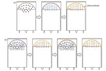
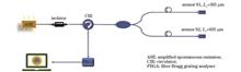
ObjectiveHigh-temperature photomultiplier tubes (PMTs) play an important role in oil logging. Till now, there has been a lack of their research and manufacturing capabilities domestically, and a significant gap in their performance compared to the world's advanced level. Therefore, it is urgent to develop independent and controllable technology for achieving domestic alternative high-temperature PMTs. The photocathode quality exerts a decisive effect on the performance of PMTs. It is necessary to optimize the photocathodes preparation techniques for high-quality photocathodes. To develop a Na-K-Sb high-temperature cathode that can be applied to high-temperature PMTs and further improve its photoelectric performance, we compare the performance of high-temperature PMTs fabricated by mono-evaporation and co-evaporation techniques and reveal the inherent mechanism affecting the performance. Additionally, we also test and evaluate the performance of the prepared high-temperature PMTs in practical applications.MethodsQuantum efficiency and photocathode sensitivity are tested to explore the effects of preparation techniques on the properties of high-temperature PMTs. The ability to distinguish energy peaks is studied by measuring the 137Cs energy spectrum after coupling PMTs with NaI (Tl) scintillation crystals using a multi-channel analyzer. The plateau characteristic curves of high-temperature PMTs prepared by different techniques are measured. To explore the underlying reasons for different performances, we test spectral response curves and high- and low-temperature curves on the two high-temperature PMTs. Meanwhile, the film thickness and surface morphology information of the Na-K-Sb high-temperature photocathode prepared by the two techniques are analyzed by scanning electron microscope, which can reveal the microscopic mechanism. The high-temperature PMTs coupled with high-temperature scintillators are placed in a chamber at 175 °C to study their performance in practical applications.Results and DiscussionsThe test results show that the high-temperature PMTs prepared by the co-evaporation technique exhibit better performance. Compared with the PMTs prepared by the mono-evaporation technique, the quantum efficiency is increased by 55.4% and the photocathode sensitivity is enhanced by 88.3%, with the energy resolution increasing by 15.7% and counting stability improving by 56.9%. This indicates that the proposed co-evaporation preparation technique is more suitable for preparing high-temperature PMTs with high performance. The analysis of the spectral response curve and the high- and low-temperature curves shows that the essential reason for significant performance improvement of PMTs prepared by the co-evaporation technique is that the Na-K-Sb high-temperature photocathode prepared by the co-evaporation technique has better photoelectric emission ability and weaker thermionic emission ability. The microscopic mechanism of different photoelectric emission ability and thermionic emission ability for the high-temperature photocathode is further revealed by microscopic characterization. It reveals that the Na-K-Sb high-temperature photocathode prepared by the co-evaporation technique has a more uniform thickness, a denser and smoother film, and better morphology uniformity. In practical applications, the prepared high-temperature PMTs show relatively poor energy resolution, plateau characteristics, and gain at 175 °C compared with like products internationally.ConclusionsWe study the effects of photocathode preparation techniques on the performance of high-temperature PMTs. The two preparation techniques for preparing high-temperature Na-K-Sb photocathodes are introduced, and their effects on the performance of PMTs are compared. The test results indicate that PMTs prepared by the co-evaporation technique have better quantum efficiency, cathode radiant sensitivity, energy resolution, and plateau characteristics. By analyzing the spectral response curve and high- and low temperature curves, we can conclude that the photocathode prepared by the co-evaporation technique has stronger photoelectric emission capacity and weaker thermionic emission ability, which is the fundamental reason for the performance improvement. Combined with the microscopic morphology characterization analysis, it is found that the photocathode film layer prepared by the co-evaporation technique is denser, smoother, and more uniform, which reveals the underlying mechanism for the different photoelectric emission and thermionic emission abilities between the two techniques. This mechanism can be applied to prepare other photocathode types, which helps promote the development of high-performance PMTs. In practical applications, the prepared high-temperature PMTs still show relatively poorer performance than like products internationally. Thus, advanced research on noise reduction of photocathode and CuBe sensitization technique is needed to improve the performance of high-temperature PMTs to the international advanced level.
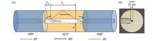
ObjectiveIn recent years, with the development of fiber optic sensing technology and increasing environmental monitoring demands, simultaneous multiple parameter measurement has caught more attention. However, currently various available sensors can only achieve measurement of 1-2 parameters, making it difficult to meet the requirements for simultaneous multiple parameter measurement in complex environments. For example, in structural health monitoring of large buildings such as bridges, it is necessary to simultaneously monitor strain, temperature, and humidity. However, existing sensor solutions mostly rely on multiple sensors for simultaneous measurement or adopt cascaded structures for three-parameter measurement, which is generally complex and costly. Therefore, the utilization of a single structure to achieve simultaneous monitoring of temperature, humidity, and strain in a multi-parameter fiber optic sensor has research significance. We propose a fiber optic sensor for simultaneously measuring temperature, humidity, and strain based on a single-mode-hollow-core-single-mode (S-H-S) structure. By utilizing the S-H-S structure to excite the coexistence of Fabry-Perot (FP), Mach-Zehnder (MZ), and anti-resonance (AR) effects, the simultaneous measurement of temperature, humidity, and strain is achieved within a single structure. We hope that our research can provide a more stable, low-cost, and compact solution for bridge health monitoring.MethodsWe achieve simultaneous measurement of three parameters by utilizing the coexistence of three sensing mechanisms in the S-H-S structure. Firstly, the coexistence principles of the three mechanisms are analyzed, and the performance parameter calculation formulas for FP, MZ, and AR effects are derived in this structure. Meanwhile, we analyze the generation principle of the AR effect, fabricate S-H-S structures with different structural parameters, and test the influence of structural parameters on sensing performance. Then, S-H-S structures with optimal parameters are fabricated and GO-PVA thin films are coated on the air-core fiber to enhance humidity sensitivity. The sensor performance changes before and after sensitivity enhancement are tested. In response to the humidity sensitivity varying with humidity changes, the humidity sensitivity range has been divided into two segments based on the application scenario, which leads to a higher linear correlation of humidity sensitivity. Finally, a temperature, humidity, and strain testing platform is set up to conduct performance tests for the three parameters. The matrix method is employed to eliminate cross-sensitivity among the three parameters, enabling the simultaneous measurement of the three parameters.Results and DiscussionsThe proposed S-H-S structure achieves the sensing mechanism coexistence of FP, MZ, and AR effects. In this structure, when the air core size of the hollow core fiber (HCF) is smaller than 10 μm, the reflection and transmission spectra of the S-H-S structure coexist with these three sensing mechanisms. The reflection spectrum of this structure exhibits FP interference and the envelope of AR fringes, while the transmission spectrum shows the superposition of MZ interference and AR (Fig. 3). S-H-S structures with different structural parameters are fabricated (Fig. 4), and the changes in reflection and transmission spectra under different parameters are compared (Figs. 5–7) to determine the optimal parameters for yielding the desired spectral fringe effects. The S-H-S structure is coated with GO-PVA to enhance sensitivity, improving the relative humidity sensitivity by 32%-715% (Fig. 9). Sensitivity tests for temperature, relative humidity, and strain demonstrate that the highest temperature sensitivity is 22.4 pm/℃ (Fig. 10), the highest relative humidity sensitivity is 37.5 pm/% (Fig. 11), and the highest strain sensitivity is 1.22 pm/με (Fig. 12). The temperature, relative humidity, and strain sensing of the sensor exhibit good linearity and stability within the target range. Comparison reveals that the proposed sensor outperforms traditional approaches in terms of smaller size, better performance, and lower cost.ConclusionsWe analyze the coexistence of FP, MZ, and AR effects in the S-H-S structure. The modulation effects of different parameters on the three mechanisms are discussed to highlight the flexibility of this structure in multi-parameter sensing. To meet the needs of bridge structural health monitoring, we design a optical fiber sensor capable of simultaneous measurement of temperature, humidity, and strain, and utilize GO-PVA hybrid sensitization. Experimental results demonstrate that the sensor achieves a maximum temperature sensitivity of 22.4 pm/℃, a maximum humidity sensitivity of 37.5 pm/%, and a maximum strain sensitivity of 1.22 pm/με, all with good linearity. By adopting transfer matrix techniques to eliminate cross-sensitivity, the simultaneous measurement of the three parameters is achieved within a single structure. The proposed sensor ensures performance and enables the simultaneous measurement of multiple parameters, while the single structure reduces the sensor's size and cost. It has significant application potential in areas such as long-distance bridge monitoring.
ObjectiveExtrinsic Fabry-Perot interferometers (EFPIs) are widely used in fiber optic sensors. In many applications, the measurand is a mixture of static and dynamic signals. However, laser interference demodulation algorithms used for dynamic signal measurement are significantly different from white light interference demodulation algorithms used for static signal measurement. Laser interference demodulation algorithms require laser wavelengths to remain stable, while white light interference demodulation algorithms require wavelength scanning to obtain the spectrum of the sensor to achieve measurement. Therefore, these measurement techniques can only measure different dynamic signals or different static signals and cannot achieve measurement of static/dynamic composite signals. For EFPI sensors, it is expected to achieve the measurement of static/dynamic composite signals through high-speed white light interferometry demodulation technologies. However, these demodulation technologies are still unable to meet the measurement requirements of high-frequency signals due to limitations in scanning speed. Some high-speed white light interferometry demodulation technologies rely on high-tuning-speed laser sources, but the bandwidth of such light sources is narrow, which limits the measurement range. At the same time, this type of technology requires a large amount of calculations and sometimes requires offline signal processing. Various laser interference demodulation algorithms have been proposed to extract dynamic signals from EFPI sensors. However, these demodulation techniques will collapse if the EFPI cavity length changes significantly since the cavity length and laser wavelengths must be strictly matched to obtain orthogonal signals. In this article, a correction symmetrical demodulation method for the measurement of static/dynamic composite signals is proposed. Static/dynamic composite signal demodulation is experimentally demonstrated.MethodsThe change in sensor cavity length is judged by the direct current component of the output signal of the symmetrical demodulation method. Then, the output signal is divided into stable segments and abrupt segments. The measurand is then re-demodulated segment by segment to improve the demodulation accuracy of the dynamic component. Phase differences calculated before and after the abrupt segment are used to compensate for the change in cavity length, and the demodulation accuracy of static components is improved. The process of static/dynamic composite signal demodulation is as follows: 1) the preliminary demodulation signal df is recovered through Eq. (11). 2) the signal df is divided into stable segments and abrupt segments. 3) the phase difference δ for each stable segment is calculated. 4) the average value of δ before and after the abrupt segment is used as the phase difference of the abrupt segment to re-demodulate the signal. Eq. (4) is then used to calculate cavity lengths before and after the abrupt segment, and the cavity length change of the abrupt segment is calibrated. 5) the measurand of each stable segment is re-demodulated and combined with the calibrated abrupt segment demodulation signals to obtain the complete output signal ds.Results and DiscussionsStatic/dynamic composite signals can be demodulated by the proposed demodulation method, which is experimentally demonstrated, as shown in Fig. 4. The cavity length change of the c-sym in Fig. 4(a) is 50.86 μm, which is consistent with the cavity length change measured by the white light interference demodulation algorithm. The measurement error of the static component is 2.07%. Figures 4 (b)-(e) show that the dynamic component of the c-sym remains consistent despite the cavity length changes significantly. The peak-to-peak amplitudes are 408.33 nm, 407.58 nm, and 402.17 nm. The amplitude variation is 1.53%. The power spectrum of the dynamic component of the c-sym is plotted in Fig. 5. The frequency is 100 Hz, which is consistent with the frequency of the input signal. The proposed demodulation method can be performed normally even if the cavity length changes up to 100 μm, as shown in Fig. 6. The frequency range of the proposed demodulation method is consistent with that of the symmetrical demodulation method and is not limited by the demodulation principle. The frequency range of the demodulator is only limited by the sampling frequency of the analog-to-digital converter and the bandwidth of electronic devices such as photodiodes. The analog-to-digital converter of the demodulator has a sampling frequency of 200 kHz. According to the Nyquist sampling theorem, the maximum frequency of the signal which the demodulator can demodulate is 100 kHz.ConclusionsIn conclusion, a correction symmetrical demodulation method for the measurement of static/dynamic composite signals is proposed. The demodulation capability of the demodulator to static/dynamic composite signals is experimentally investigated. The measurement of a cavity length change with an amplitude of 100 μm is achieved. The measurement error is about 2% for large changes in cavity length. The technique is applicable to static/dynamic composite signals applied on sensors with different cavity lengths.
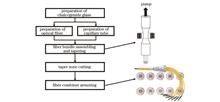
ObjectiveIn recent years, mid-infrared lasers have caught increasing attention because of their significant applications in a number of fields such as defense security, environment monitoring, and medical surgery. They mainly include solid state laser, gas laser, optical parametric oscillator, quantum cascade laser (QCL), and fiber laser. Among them, since QCL features small size, lightweight, and ultra-wide wavelength coverage (3-13 μm commercially available currently), it is considered a promising compact and practical mid-infrared laser. However, the output power of a single QCL is limited to 10 W level. Laser beam combining technology is considered an effective way to significantly improve the output power of QCL. In this technology, a higher power level is achieved by superposing the output power of multiple lasers. Compared with spatial beam-combining technologies such as spectral beam combining and coherent beam combining, optical fiber beam-combining technology has the advantages of compact structure and good robustness, and is the preferred technology for improving the output power of QCL. Thus, we aim to develop a compact mid-infrared combiner for the power enhancement of QCL.MethodsAs-S chalcogenide glass is employed to fabricate the optical fiber combiner because of its excellent thermal stability against crystallization and relatively high laser damage threshold. The chemical compositions of the core and cladding glass are As40S60 and As38S62 respectively. The fabrication of 7×1 fiber combiner includes the preparation of high-purity glass, optical fiber, and capillary tube, fiber bundle assembling and tapering, taper zone cutting, and fiber combiner armoring. The As40S60 and As38S62 chalcogenide glasses are prepared in low-OH quartz tubes by the vacuum melt-quenching method. The As-S optical fiber is fabricated by the rod-in-tube method, the cladding tube is by the rotational method, and the As38S62 capillary tube is by the combination of extrusion and thermal-drawing methods. The fiber bundle tapering is conducted on a self-made longitudinal tapering system. First, seven fibers with a length of about 50 cm are cut out, and one end of the fiber (about 8 cm long) is immersed in dimethylacetamide (DMAC) solvent to dissolve the surface polymer. The polymer-free ends of the seven fibers are then inserted into the As38S62 capillary tube with a length of about 12 cm, and the capillary tube is glued with the fiber bundle using a high-temperature adhesive. Subsequently, the fiber bundle is placed into the tube furnace of the longitudinal tapering system, the fiber-free end of the capillary tube is connected to a vacuum pump to maintain lower pressure inside the capillary tube, and the fiber bundle is tapered at about 270 ℃. Finally, the tapered region of the fiber bundle is cut and the obtained fiber combiner (without fusing output fiber) is armored.Results and DiscussionsThe fabricated As40S60/As38S62 fiber has a core diameter of 200 μm and a cladding diameter of 250 μm. It shows good transmission performance in the 2-6.5 μm with a background loss of about 0.5 dB/m. The losses at 3 μm and 4.6 μm are (0.56±0.04) dB/m and (0.63±0.05) dB/m respectively. Based on the fabricated fiber, the 7×1 fiber combiner is designed. The numerical simulation shows that the appropriate taper reduction ratio Ris 2-4, and the length of the taper transition zone should be more than 500 μm. Following the design, 7×1 fiber combiners with R of 3 and 4 are fabricated (Fig. 8). The taper transition zone is about 2 cm long. The cross-sectional images of the output end of the fiber combiners show that the fiber monofilaments are arranged in a good regular hexagonal shape, and the fiber bundles do not undergo significant deformation after being tapered. The measurements show that the port transmission efficiency ηof the fiber combiner is 90.7%-92.5% at 3 μm and 87.2%-90.8% at 4.6 μm when R=3, and it is 88.1%-91.4% and 85.1%-87.5% at 3 μm and 4.6 μm respectively when R=4 (Table 1).ConclusionsWe develop a 7×1 chalcogenide glass fiber combiner and investigate its mid-infrared transmission properties. The fiber combiner is formed by fusing and tapering an As40S60/As38S62 fiber bundle. The core and cladding diameters of the individual fiber are 200 μm and 250 μm respectively, with the numerical aperture of 0.38-0.35 (@ 2-6 μm). The taper ratio R of the final fiber combiner is 3 or 4, and the length of the taper transition zone is about 2 cm. The results show that when R=3, the port transmission efficiency of the fabricated fiber combiner at 3 μm and 4.6 μm is more than 90% and 87% respectively, and when R=4, it is more than 88% and 85% respectively. There is no obvious crosstalk between the fiber monofilament at the output end of the fiber combiner. The results indicate that the fabricated fiber combiner is an efficient laser combining device and is promising in mid-infrared laser power enhancement and wide spectrum synthesis.
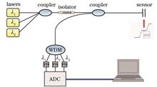
ObjectiveOptical fiber extrinsic Fabry-Perot interferometer (EFPI) sensing technology measures external physical quantities by detecting interference spectrum changes caused by variations in the sensor cavity length or refractive index of the medium inside the cavity. Compared to traditional sensing techniques, the EFPI sensor features high sensitivity, small size, and immunity to electromagnetic interference, and has extensive applications in measuring physical quantities such as pressure, temperature, vibration, displacement, and acceleration. Optical fiber EFPI sensors have been widely applied to aerospace, energy exploration, underwater acoustics, and defense industries, playing an increasingly important role. In complex environments, a single sensor often fails to provide detailed information about the target, which necessitates the integration of multiple sensors into an array for more accurate measurement. However, in optical fiber sensor arrays, crosstalk occurs during the transmission and demodulation of optical signals, and it is the interference among different channel signals. When the crosstalk in a multiplexing system exceeds -40 dB, the multiplexing capacity will be decreased with significant signal detection bias. Therefore, crosstalk has become a challenging problem hindering the development and applications of multiplexing technology in optical fiber sensor arrays. We propose a five-step phase shift demodulation scheme based on multi-wavelength demodulation. Compared to a single-wavelength demodulation scheme, the multi-wavelength demodulation scheme averages the demodulation results of the five-step phase shift signals at multiple consecutive operating points, reducing crosstalk in the sensor array and improving the interference resistance and reliability of the sensing system. Moreover, this demodulation scheme lowers the requirements for the extinction ratio of the optical switches in the sensor array and the cavity length consistency among different elements, thus promoting the development of large-scale multiplexing in optical fiber F-P sensor arrays.MethodsThe interference spectrum of the F-P sensor is obtained by utilizing white light interference (WLI) technology. The spectrum is sampled at regular intervals in terms of wavelength, and preliminary spectral data processing is performed by eliminating the envelope and fitting an ellipse. When the reflection spectrum has N wavelengths, Ns groups of five-step phase shift interference signals can be obtained. The phase relationship between each group of five-step phase shift interference signals is adopted to yield two orthogonal signals, and the changes in the beginning phase are derived by an arctangent algorithm. According to the relationship between phase and cavity length, averaging Ns groups of phase changes can be utilized to determine the dynamic cavity length changes of the F-P sensor. The feasibility of the proposed scheme is validated via numerical simulations. Compared to single-wavelength demodulation schemes, the multi-wavelength demodulation scheme reduces the impact of fundamental frequency crosstalk (FFC) and total harmonic crosstalk (THC). This scheme employs spectral information from multiple different wavelength sources and thus reduces crosstalk at different wavelengths, which allows the sensing signal to be transmitted and processed more accurately and stably.Results and DiscussionsAs the extinction ratio increases, both FFC and THC exhibit an approximately linear decreasing trend. Meanwhile, the FFC and THC of the multi-wavelength demodulation scheme are significantly lower than those of the single-wavelength demodulation scheme. When the extinction ratio reaches 25 dB, the FFC of the multi-wavelength demodulation scheme can be reduced to below -50 dB, while the single-wavelength demodulation scheme requires an extinction ratio of over 45 dB to achieve the same crosstalk level (Fig. 2). Furthermore, when the number of average wavelengths Ns=nλ02/2ΔλΔLint, the multi-wavelength demodulation scheme shows the best crosstalk suppression capability (Fig. 3). Additionally, both FFC and THC reach their minimum values when the demodulation parameter is close to π/2 radians, providing solid theoretical basis for the applications of the proposed scheme in optical fiber F-P sensor arrays (Fig. 5). As the cavity length differences increase, FFC and THC gradually exhibit fluctuations. This indicates that the multi-wavelength demodulation scheme can better suppress crosstalk under certain differences in the cavity lengths of elements S1 and S2 (Figs. 6 and 7).ConclusionsA five-step phase-shift demodulation scheme based on multi-wavelength averaging is proposed to suppress crosstalk in optical fiber F-P sensor arrays. A parallel multiplexing system based on fiber F-P sensors with two elements is established, and the crosstalk in the system is subjected to theoretical analysis and numerical simulations. The results indicate that the crosstalk magnitude among different channels in the sensor array is related to the extinction ratio ε, the average wavelength number Ns , the wavelength interval Δλm, and the cavity length variation among different elements. Numerical simulations conducted with controlled variables show that the FFC and THC of the multi-wavelength demodulation scheme are significantly lower than those of the single-wavelength demodulation scheme. Furthermore, the proposed scheme can meet the crosstalk requirements of the array with a lower extinction ratio, enabling the composition of larger-scale fiber F-P sensor arrays. Additionally, it exhibits better crosstalk suppression among elements with different cavity lengths, addressing the issue of cavity length consistency among different elements in the optical fiber F-P sensor array. This greatly reduces the fabrication complexity of the sensors and improves the scalability of the multiplexing system.
ObjectiveTraditional single-wavelength fiber lasers make it challenging to meet the increasing capacity demands for modern optical fiber communication systems. Employing multiple single-wavelength fiber lasers as light sources by wavelength division multiplexing technology is bound to increase system complexity and costs. Additionally, there are potential applications in multi-dimensional information fiber sensing for multi-wavelength fiber lasers. Therefore, multi-wavelength fiber lasers with stable performance have been widely studied and can be adopted to expand communication systems and meet the needs of multi-dimensional information fiber sensing. However, the problems for stable operation of multi-wavelength erbium-doped fiber laser (EDFL) are as follows. At room temperature, due to the homogeneous broadening of erbium-doped fiber, it is easy to cause mode competition, which reduces the stability of multi-wavelength fiber lasers with narrow wavelength intervals. Based on the dual-wavelength linear cavity EDFL, we select a simple linear cavity fiber laser structure, optimize the reflectivity and center wavelength of fiber Bragg grating (FBG), and realize a stable dual-wavelength laser output by the polarization hole burning (PHB) effect. Compared with the existing PHB schemes, the laser features a simple and compact structure, low cost, and good stability. We hope that our study will help realize dual-wavelength linear cavity fiber lasers with excellent performance at room temperature.MethodsWe study the influence of the structure of dual-wavelength linear cavity EDFL and FBG parameters (reflectivity and center wavelength) on the output performance of a dual-wavelength laser. Firstly, the output power and dual-wavelength laser spectra of 3 dB fiber loop mirror (FLM) and high reflectivity-FBG (HR-FBG) as the total reflector respectively, and low reflectivity-FBG (LR-FBG) as the output mirror are compared. Secondly, based on the double fiber Bragg gratings (DFBGs) as a cavity mirror, two HR-FBGs with the same reflectivity are adopted as the total reflector. The output power, dual-wavelength laser spectra, and power stability with the same reflectivity and different reflectivities are compared when two LR-FBGs are utilized as the output mirror. Finally, based on the first two groups of experiments, DFBGs are leveraged to constitute the cavity, and the reflectivities of the two HR-FBGs and the two LR-FBGs are equal respectively. The output power and dual-wavelength laser spectra of DFBGs with different center wavelength intervals (?λ of 4, 8, and 12 nm) are compared. Additionally, the long-term laser stability is analyzed, which includes the temporal stability of spectra, center wavelength changes, power fluctuations, and 3 dB bandwidth stability.Results and DiscussionsFirstly, the contrast experiment is carried out based on dual-wavelength linear cavity EDFL with FLM and HR-FBG structures. The results show that the slope efficiency of the two EDFL structures is basically equal. The optical signal-to-noise ratio (OSNR) based on the HR-FBG structure is still higher than that based on the FLM structure (Fig. 7), which indicates that the laser output performance of the linear cavity EDFL based on the HR-FBG structure is better. Secondly, in the dual-wavelength linear cavity EDFL based on HR-FBG structure, the influence of the same and different reflectivities of LR-FBG on the EDFL output performance is studied. The contrast experiment shows that the slope efficiency and OSNR of the two LR-FBGs with the same reflectivity are higher than those with different reflectivities, and the output power is more stable (Fig. 8). Finally, we study the effect of varying center wavelength intervals of DFBGs on the EDFL output performance. The contrast experiment shows that as the center wavelength interval of DFBGs gradually increases, the slope efficiency of the dual-wavelength linear cavity EDFL gradually decreases, and the OSNR of the two wavelength lasers gradually rises (Fig. 9). By adjusting the polarization controller (PC), the dual-wavelength laser output spectra of EDFL with three wavelength intervals will not hop with time. Constantly, the larger center wavelength interval leads to smaller center wavelength changes (Fig. 10), and smaller output power fluctuations and 3 dB bandwidth (Fig. 11).ConclusionsWe realize a dual-wavelength linear cavity EDFL based on DFBGs with a simple structure and output a stable dual-wavelength laser at room temperature by the PHB effect, with the output performance analyzed. The results show that the output performance of the HR-FBG structure is better than that of the FLM structure. When the reflectivities of the two LR-FBGs adopted as the output mirror is the same, the output performance is better than that under different reflectivities. Additionally, as the center wavelength interval of DBFGs gradually increases, the OSNR of EDFL gradually improves, and the dual-wavelength laser output gradually stabilizes, but its slope efficiency will decrease due to the gain characteristics of EDF at different wavelengths. Finally, we realize that the stable results in dual-wavelength linear cavity EDFL with the OSNR of 1550 nm and 1562 nm are about 50.24 dB and 51.19 dB. The center wavelength fluctuations are less than 0.030 nm and 0.035 nm, and the power fluctuations are less than 0.061 mW and 0.059 mW, with 3 dB bandwidth of ~0.146 nm and ~0.144 nm respectively. The output results are better in the dual-wavelength linear cavity.
ObjectiveWith the development of fiber communication, traditional multiplexing techniques cannot meet the demands for capacity. The utilization of orbital angular momentum (OAM) modes to carry information is a way to implement space division multiplexing (SDM) technology. This approach can greatly increase the capacity and spectral efficiency of fiber communication and show broad application prospects due to its unique advantages. Currently, transmitting OAM modes based on photonic crystal fiber (PCF) structures face problems such as difficulty in preparation and high loss. As research deepens, scholars attempt to solve these problems by utilizing anti-resonance fiber (ARF) to transmit OAM modes. The Fresnel reflection of the negative curvature tube in ARF cladding can enhance the confinement of the fiber core to the beam, further reducing the confinement loss (CL). Additionally, the preparation method of ARF is simpler than that of PCF, and fewer structural parameters make ARF easier to optimize for enhancing fiber performance. However, there is still a low number of transmission OAM modes in the current ARF design. Based on this, we propose an ARF composed of two sets of negative curvature anti-resonance tubes with different sizes. By introducing high refractive index materials in the ring core, more OAM modes can be transmitted, thereby improving the capacity of the fiber communication system.MethodsAn ARF is designed by introducing high refractive index materials into the ring core to organically combine total internal reflection and anti-resonance guiding mechanisms. In this ARF, the OAM mode is limited by total internal reflection in the ring core and the Fresnel reflection from the negative curvature tube of the cladding, which realizes the stable transmission of OAM modes in the fiber. Its structure includes a central air hole, an inner layer of high refractive index amethyst glass tube, an intermediate layer silica (SiO2) glass tube, and an outer layer of negative curvature tube. As the OAM mode number determines the capacity of the fiber communication system, and the radius of the central air hole, the thickness of Amethyst and SiO2 glass tubes are key factors affecting the OAM mode number. First, the control variates are adopted to optimize the three key parameters of ARF at the 1.55 μm wavelength. Considering the influence of dispersion on stable OAM mode transmission, the optimal structural parameters of ARF are determined by optimizing the thickness of the SiO2 glass tube, with the fundamental mode HE1,1 as the observation term. The optimization takes into account both the OAM mode number and dispersion. Based on this, the fiber bending resistance is analyzed. Secondly, considering the practical fiber applications, it is necessary to have a certain operating bandwidth. Therefore, the stable OAM mode transmission and fiber transmission characteristics in 1.5-1.7 μm are analyzed and discussed. Additionally, the effective refractive index, effective refractive index difference, dispersion, CL, mode purity, effective mode-field area, nonlinear coefficient, and numerical aperture (NA) are included. Finally, the effect of preparation errors on the fiber properties is analyzed and discussed.Results and DiscussionsFirst, in ARF, total internal reflection and anti-resonance are organically combined to support stable transmission of 130 OAM modes in 1.5-1.7 μm bands, which can greatly increase the capacity of the fiber communication system. Secondly, the transmission characteristics are analyzed, and the results show that the introduction of high refractive index materials in the core results in a larger effective refractive index difference ?neff between adjacent hybrid modes, with a maximum value of 6.08×10⁻³ (Fig. 9), which can inhibit the degradation of the OAM modes into linearly polarized (LP) modes. By optimizing the thickness of the intermediate layer SiO2 glass tube, the dispersion changes of the hybrid modes all exhibit a flat state, with a minimum dispersion change of 0.43 ps/(nm·km) (Fig. 10). A flat dispersion is beneficial for dispersion compensation. The negative curvature tubes in the outer layer are all in the anti-resonance state, which further enhances the restriction on photonic energy of the ring core and reduces the CL. The CL of hybrid modes maintains between 10-14-10-8 dB/m (Fig. 11). It is shown that this design ensures a large OAM mode number and has good fiber transmission characteristics and simplifies fiber preparation.ConclusionsWe design an ARF that supports stable OAM mode transmission and features excellent transmission characteristics and relatively simple preparation. Based on the finite element method, the ARF is modeled and simulated. The results show that 130 OAM modes can be stably transmitted within the range of 1.5-1.7 μm, a maximum effective refractive index difference is 6.08×10⁻³,and the minimum dispersion change rate is only 0.43 ps·nm-1·km-1. The CL maintains in the range of 10-14-10-8 dB/m and the highest mode purity reaches 99.26%. The maximum effective mode-field area is 187.38 μm2, the minimum nonlinear coefficient is 0.87 W-1·km-1, and NA is concentrated between 0.064-0.086. The proposed ARF applied to SDM has higher communication capacity and spectral efficiency and provides references for the study of transmitting OAM modes by anti-resonant structures.
ObjectiveElectro-optic modulators can change the phase and polarization state of incident light, therefore having a wide range of applications in many fields, such as optical communication, integrated optics, and super-resolution microscopy. They feature fast response and reliability. However, due to the differences among electro-optic modulator devices, the relationship between the applied voltage and the phase change in actual operation is not consistent with the corresponding relationship in the technical manuals. Meanwhile, when modulators are working at different wavelengths, applying the same voltage to the modulator results in different phase changes. Therefore, before utilization, it is necessary to calibrate the relationship between the phase change and voltage change of the electro-optic modulator. Since its modulation is linear, the slope of the function only needs to be obtained for subsequent experiments.Common calibration methods include the contour method and the Michelson interferometry method. The contour method employs two optical paths for interference, one of which passes through an electro-optic modulator to change the phase. Interference fringes are taken at a certain voltage interval. The displacement between two fringes is divided by the fringe period and then multiplied by 2π to obtain the phase difference which is combined with the voltage interval to get the half-wave voltage. This method is simple but requires repeated adjustment and correction, which is time-consuming and laborious. Additionally, the limitation of camera pixels reduces the accuracy. The Michelson interferometry method passes one of the interferometer arms through an electro-optic modulator, applies a voltage to produce a phase shift, and then moves this arm to change the optical path difference and make the interference fringes disappear to determine the phase difference. This method has high accuracy but requires optical path rebuilding with too much consumed time.To quickly and accurately calibrate the half-wave voltage of an electro-optic modulator without rebuilding an optical path, we study a method using cross-correlation in the frequency domain. The complex conjugate of the high-order spectrum of the previous interference fringe is multiplied by the high-order spectrum of the subsequent fringe to calculate the phase difference for calibrating half-wave voltage.MethodsWe adopt the phase angle of the cross-correlation function between multiple fringe images to determine the phase difference. After converting the fringe illumination light to the frequency domain, the high-order spectrum is extracted. In the spectra of multiple fringe patterns, the conjugate of the high-order spectrum of the previous one is multiplied by the next one to obtain the cross-correlation function of adjacent images. The angle of this function is the phase difference between two fringe images. The feasibility of this method is verified by generating fringe images with the same phase difference in Matlab. The optical path for experimental calibration is part of a structured illumination super-resolution microscopy system. This system achieves high-speed imaging based on electro-optic modulators and galvanometers. One optical path passes through a phase electro-optic modulator, while the other does not. Finally, the two beams interfere at the camera through a mirror to form fringes.Results and DiscussionsThe experiment applies voltage to the EOM through a computer-controlled acquisition card, with a voltage interval of 1 V and a voltage range of -10 V to 9 V. When the voltage is changed each time, the camera is controlled to acquire an image and save it. A total of 20 interference fringe images with equal interval displacement are collected. The 640 nm and 561 nm lasers are utilized for calibration, and the calibration results of the Michelson interferometry method serve as the correct results for accuracy consideration. To further eliminate the errors caused by interference, we take nine sets of fringe images for each laser wavelength, calculate the average value of the nine sets of results, and then compare this value with the accurate calibration value. The half-wave voltage obtained by calibrating the 640 nm using the Michelson interferometry method is 6.6 V, and the result obtained using this method is 6.57 V, with a difference of 0.03 V and an error of 0.45%. The half-wave voltage obtained by calibrating the 561 nm using the Michelson interferometry method is 5.87 V, and the result obtained by this method is 5.84 V, with a difference of 0.03 V and an error of 0.51%. After converting to phase difference, the phase difference calculated for 640 nm is 0.478 rad, the standard phase difference is 0.476 rad, and the difference is 0.002 rad. The phase difference calculated for 561 nm is 0.538 rad, the standard phase difference is 0.535 rad, and the difference is 0.003 rad. By employing the contour method to process the 640 nm image, the obtained half-wave voltage is 6 V, which has a larger error than the result obtained by this method. The half-wave voltage obtained by our method is close to that obtained by the Michelson interferometry method, with the same accuracy and faster speed.ConclusionsBefore adopting an electro-optic modulator, it is often necessary to calibrate the half-wave voltage. Previous methods such as Michelson interferometry require additional optical path construction, and the calibration process is slow and easily interfered by noise and jitter. Thus, the contour method is not accurate enough. Therefore, a method based on the high-order cross-correlation of the interference fringe frequency domain is proposed to calculate the phase difference between fringe images and calibrate the half-wave voltage of the electro-optic modulator. This method employs a specific mask to remove the 0th-order spectrum and extract the high-order spectrum. The complex conjugate of the high-order spectrum of the previous image is multiplied by the high-order spectrum of the next image to obtain the angle and then solve for the phase difference. The phase error in actual detection reaches 0.002 rad and the half-wave voltage error is 0.03 V, which meet the calibration requirements of electro-optic modulators. Since the proposed method has a large calibration speed and does not require optical path rebuilding, it can check whether the electro-optic modulator drifts at any time and whether corrections are needed or not.
ObjectiveThe continuous development of 3D display technology has brought society a new research field. Since 3D display technology based on computer generated hologram (CGH) features flexibility, repeatability, and convenience, most universities and research organizations have conducted in-depth research on it. With the increasing research on CGH theory and improving the performance of spatial light modulator (SLM) device structures, applications based on SLM have gradually become a research hotspot in holographic projection, holographic displays, virtual reality/augmented reality (AR/VR) displays, dynamic holography, and color holography. In 3D display, there is a multi-plane display method whose essence is between 2D and 3D, and the method employs a hologram that can display the same or different results at multiple locations. However, there are two main problems in the multi-plane holographic display. One is that the decreased reconstruction quality will accompany the increased number of planes in a multi-plane holographic display, and the other is the non-uniform distribution of the reconstruction image quality among each plane. The main reason is that the planes will interfere with each other, and the interference is random and relatively difficult to control. To improve multi-plane holographic display quality, we propose an improved weighted iterative multi-plane holographic display method. Meanwhile, to reduce the mutual influence among the planes in designing holograms, we introduce weights to control the constraints, and thus the quality distribution of the reconstructed images among multiple planes is more uniform and of higher quality by the constant correction of the weights during the calculation. The results show that the introduction of this method not only does not reduce the calculation speed but also leads to a more uniform quality distribution of the reconstructed image in the multi-plane holographic display. Additionally, the quality is improved to some extent, which provides a new idea for high-quality multi-plane display.MethodsOur design idea is based on the Gerchberg-Saxton (GS) iterative algorithm and is further improved by introducing weights on the holographic plane. Firstly, the output plane complex amplitude is composed according to the amplitude information of the known multi-plane target with random phases. Then, the inverse diffraction is carried out into the holographic plane at a known distance, and all complex amplitudes in the holographic plane are summed up in the weights. The total complex amplitude distribution of the holographic plane is obtained, and the weights are distributed in a weighting. In assigning the weights, the sum of all the weights should be 1. Initially, the weights of each plane are set to be equal. Then, the weights are corrected iteratively by the iterative optimization algorithm according to the CC value changes, and the purpose of setting the weights is to reduce the mutual influence among the planes. After summing up the weights, we ensure that the influences of the planes are balanced to make the distribution among the planes more uniform. Then we take the phase, keep it unchanged, and combine it with the plane wave amplitude to get the complex amplitude distribution of the holographic plane. Meanwhile, forward diffraction is conducted again to obtain the complex amplitude distribution of the output plane, then its phase is taken and combined with the target amplitude. This process is repeated until the results are satisfied.Results and DiscussionsOur core content is the weight correction for each plane, the specific correction idea is shown in Fig. 2, and the specific formulas for the correction are Eqs. (3)-(6). For two-plane holography, the quality of reconstructed images in each plane without introducing weights will be randomly distributed, and the reconstructed images in each plane will be qualitatively different when the introduction of the weights among various planes makes the reconstruction of the image distribution quality uniform (Figs. 4 and 12). It is discussed that for each plane with the same or different target images (Fig. 9), the quality of the reconstructed images of various target image types is different. Specifically, the quality of reconstructed images is relatively high under the same target images, and the quality of reconstructed results is poor when the target images are not the same. The differences between the two will become increasingly larger with the rising number of planes. Under the small number of planes, whether the target image is the same has little effect on the quality of the reconstructed image, and under the large number of planes, the quality of the reconstructed image is affected by whether the target images are the same or not (Figs. 6 and 10). For multi-plane holography, the most significant influence is the target image type, the number of planes, and the distance between neighboring planes (Figs. 13 and 14).ConclusionsTo reduce the mutual influence among the planes in the multi-plane display, we propose an improved weighted iterative multi-plane holographic display method by employing the weights. Finally, the control among the planes is controlled according to the interactions among the planes in the process of designing the holograms, and the distribution of the reconstruction image quality among the planes is more uniform. Additionally, without reducing the quality of the reconstructed image, the calculation speed will not be affected. The method is compared and analyzed by the simulation analysis and experimental verification of two to six different target images and the same target image to achieve a more uniform distribution of the reconstructed image quality among the planes. The quality of the reconstructed image is affected by the target image type, in which the quality is relatively high under the same target image, and it is poorer under different target images. The difference between them will become increasingly larger with the rising number of planes. In conclusion, introducing this method reduces mutual interference among reconstructed images in multi-plane holographic displays and their more uniform quality distribution.
ObjectiveOptical coherence tomography (OCT) is a pivotal biomedical imaging technique based on the low coherence interference principle. It facilitates the production of tomographic scans of biological tissues, extensively applied to medical fields such as ophthalmology and dermatology. However, the pursuit of heightened axial resolution compels OCT systems to harness broadband light sources, and it is an approach that inadvertently introduces dispersion effects and gives rise to imaging artifacts, blurring, and consequently diminished image quality. Therefore, it is necessary to conduct dispersion compensation in OCT systems. While hardware-based compensation techniques are plagued by increased costs and complexity, their efficacy remains limited, which spurs the exploration and application of more flexible dispersion compensation algorithms. However, commonly employed algorithms based on search strategies suffer from suboptimal adaptability and concealed computational intricacies. Thus, we introduce an innovative dispersion compensation algorithm established based on the concept of spatial pulse degradation resulting from dispersion. The algorithm integrated into frequency domain OCT system experiments eliminates the requirements for manual dispersion range adjustments. Meanwhile, it features notable computational efficiency to offset the shortcomings of conventional search strategies in adaptability and computational efficacy. The proposed method is proven to be instrumental in enhancing the engineering practicality of OCT systems and improving the quality of tomographic images.MethodsWe propose an efficient dispersion compensation algorithm grounded in spatial pulse degradation due to dispersion and apply it to frequency domain OCT system experiments. The algorithm consists of two parts including dispersion extraction and compensation. By adopting the principle that dispersion causes widening spatial pulse, the algorithm estimates the dispersion of the signal to be corrected and subsequently applies compensation. A linear equation establishes the relationship between the square of spatial pulse width and the square of second-order dispersion. Additional dispersion phases are generated numerically and integrated into the original spectral signal to yield new dispersion signals. After transformation to the spatial domain, these signals' spatial pulse widths are measured. By substituting these pulse width values into the equation set, the second-order dispersion of the original signal can be calculated. Finally, a dispersion compensation phase is constructed and incorporated into the original spectral signal's phase for dispersion correction.Results and DiscussionsTo validate the efficacy of this algorithm, we devise a swept source OCT (SS-OCT) system for data collection. The method is applied to correct dispersion in the point spread function (PSF) of the system and biological tissue images. The experimental results show that the algorithm's dispersion estimates exhibit a relative error of less than 10% when compared to actual dispersion values in different dispersion conditions (Table 1). After implementing this algorithm for dispersion compensation, notable enhancements are observed in the system's peak signal-to-noise ratio and axial resolution. In scenarios of similar correction efficiency, this algorithm surpasses the commonly employed iterative method by a factor of 5 in terms of speed and outpaces the fractional Fourier transform method by a remarkable 50-fold (Table 2). Furthermore, after applying dispersion compensation, the image quality is notably improved. The grape flesh image boundaries exhibit enhanced sharpness, with significantly enhanced internal tissue clarity and more concentrated image energy (Fig. 4). Additionally, human retinal images display clearer layer differentiation, accompanied by image contrast improvement (Fig. 5). These results collectively prove the algorithm's efficacy in enhancing image quality.ConclusionsWe introduce a novel high-efficiency dispersion compensation algorithm grounded in spatial pulse width. The algorithm mitigates axial broadening in PSF and enhances the system's signal-to-noise ratio. Notably, the algorithm's strength lies in its independence from prior knowledge about system dispersion or manual dispersion search interval selection. It accurately estimates system dispersion, and when compared with other search strategy-based algorithms, it demonstrates superior computing efficiency and achieves comparable compensation efficacy. The dispersion compensation experiments conducted on grape pulp and human retinal images yield effective results. The algorithm suppresses axial broadening blur, amplifies image contrast, and elucidates intricate structural features within biological tissues. These outcomes underscore the algorithm's capacity to proficiently rectify dispersion issues in OCT systems, thereby enhancing visual image quality. Nevertheless, certain limitations deserve consideration. Primarily, the algorithm's applicability is confined to addressing second-order dispersion, and higher-order dispersion tackling necessitates further exploration into the numerical relationship between spatial pulse distortion and higher-order dispersion. Furthermore, the algorithm exclusively addresses system dispersion, ignoring sample dispersion intricacies tied to specific sample structures and depths. Future research should explore depth-adaptive sample dispersion compensation, and leverage the algorithm's high computational efficiency to potentially enable depth-dependent dispersion compensation.
ObjectiveSpectroradiometers are used to determine the spectral characteristics and brightness of radiation sources, which are widely used in many different fields. This study is based on the circular variable filter type spectroradiometer, where the wavelength transmitted by the main spectroscopic component, the circular variable filter is linearly related to the angle, and the spectroradiometer is constructed with a unit detector. This type of spectroradiometer has the advantages of a wide spectral range and a wide temperature range for the target, so it has a wider range of applications. However, there are fewer studies on circular variable filter spectroradiometers in China and abroad, and the development of domestic machines for circular variable filter spectroradiometers is gradually being carried out in China. Radiation calibration is the process of converting the original signal measured by the instrument into a physical quantity with practical significance. The main methods of radiation calibration for infrared spectroradiometers are currently the single point method, the two points method, and so on. The single point method is suitable for cases with low resolution and a small amount of spectral measurement data. The two-point method is suitable for situations where the instrument has good linearity, and the number of measurement points is high. Due to the wide operating band of the circular variable filter type infrared spectroradiometer and the wide range of the target temperature, which causes non-linearity problems, the traditional two-point calibration method cannot achieve accurate radiation calibration. In this paper, a divisional linearity-based responsivity radiometric calibration method is proposed to solve this problem.MethodsThe radiometric calibration of circular variable filter spectroradiometers is based on the divisional linearity method, which is used to solve the non-linearity problem of this type of spectroradiometer due to the large temperature range of the measurement target and the wide operating band. The main technical principle is to divide the temperature interval of the target to be measured into several subintervals, collect the measured spectrums corresponding to several different temperature blackbodies in the target temperature interval, and calculate the responsivity function at each temperature. During the infrared spectroscopy measurements, the target spectrum is compared with the spectrums of different temperature points recorded in the interval to determine the upper and lower limits of the temperature subinterval to which the target to be measured belongs. Based on the responsivity function calculated for the subinterval, a linear interpolation is performed to find the responsivity function of the target to be measured for radiometric calibration. In addition, external ambient temperature variations, atmospheric disturbances, and the instrument's thermal radiation are taken into account in the calibration process.Results and DiscussionsIn this paper, we propose a divisional linearity-based responsivity radiometric calibration method, which can effectively solve the non-linearity problem caused by the wide wavelength range and wide temperature range of the target measurement by zoning the target temperature into sub-regions. We compare the difference between the measured calibration data and the theoretical Planck curve at different temperatures. Figure 12 shows the relative deviation of the radiometric calibrations of two detectors at different blackbody temperatures. Figure 12 shows that the relative deviations of the radiometric calibrations are better than 1% for most of the band intervals for both detectors. The large relative deviations in some bands are due to two reasons: 1) the low responses of the InSb detector in the 2.4-3 μm region and the MCT detector in the 13.5-14.3 μm region are due to the low signal-to-noise ratio of the collected signals in this region, which affects the calibration accuracy; 2) the InSb detector in the 4.2-4.5 μm region is due to the interference of CO2 atmospheric absorption in this band. The interference of CO2 atmospheric absorption exists. The experimental results show that this method can effectively meet the radiometric calibration requirements, and the calibration results are in good agreement with the theoretical values, with an equivalent temperature deviation of less than 2%.ConclusionsThe large temperature range and the wide operating band of the circular variable filter spectroradiometer make for a significant non-linear response in the radiometric calibration process. Different temperature targets also have different degrees of responsiveness, so the traditional two-point method does not work well for radiometric calibrations. In addition, external ambient temperature variations, atmospheric disturbances, and the instrument's thermal radiation are taken into account in the calibration process. In this paper, a divisional linearity-based radiometric calibration method is proposed, which can effectively solve the non-linearity problem caused by the wide wavelength range and temperature range of the target measurement by zoning the target temperature into sub-regions. The experimental results show that the method can effectively meet the radiometric calibration requirements, and the calibration results are in good agreement with the theoretical values, with an equivalent temperature deviation of less than 2%. The zoned linear radiometric calibration method in this paper is also applicable to other spectroradiometers of the spectral type to solve the non-linearity problem caused by the measurement of targets with a wide wavelength and temperature range.
ObjectiveSilicon-based modulators feature small size, low power consumption, and easy integration. However, compared with lithium niobate modulators, they suffer poor linearity, which limits their performance in analog communication systems such as radio over fiber access networks. Various improvement methods have been proposed to improve the linearity of silicon-based modulators, including optimizing the p-n junction design, modifying the doping concentration of the p-n junction, and adopting novel waveguide structures, electrode structures, and driving methods. However, these methods generally require altering the physical characteristics or structures of the devices or adding additional driving circuits. The modulator linearity is typically fixed once the device fabrication or packaging is completed, which makes it difficult to change afterward. Currently, there is a lack of compensation schemes for Si modulator linearity after device fabrication or packaging. Therefore, we want to propose a way from the system perspective to conduct the performance compensation caused by the poor linearity of Si modulators.MethodsIn our paper, a novel enhanced maximum-ratio combined receiver (EMRC-Rx) is proposed and demonstrated through proof-of-concept experiments, and it is conducted to mitigate the system performance degradation caused by the low linearity of Si modulators when the modulators are deployed in passive optical network (PON)-based access networks. The EMRC-Rx leverages the advantages of both direct detection receiver (DD-Rx) and lite coherent detection receiver (Lite CO-Rx) by utilizing the maximum signal-to-noise ratio contribution from both the receiver types to significantly improve receiver sensitivity and mitigate the system performance degradation. The proposed EMRC algorithm considers the contribution of multiple Lite CO-Rx components to the output signal-to-noise ratio, thereby increasing the proportion of signal-to-noise ratio in the lite coherent receiver and further enhancing the receiver sensitivity. As a result, the EMRC-Rx in the Si modulator system could achieve similar performance compared with the MRC-Rx in the lithium niobate modulator system. The EMRC-Rx consists of three components including DD-Rx, Lite CO-Rx #1, and Lite CO-Rx #2 (Fig. 3). The results of the three components are aggregated and calculated by the EMRC algorithm from Equation 1 to obtain the final output of the EMRC-Rx. The corresponding digital signal processing flow for DD-Rx, Lite CO-Rx #1, and Lite CO-Rx #2 is illustrated in Fig. 3.Results and DiscussionsThe experimental results show that when the bit error rate (BER) exceeds the KP4-FEC threshold at 1.0 × 10⁻⁴, the receiver sensitivity of EMRC-Rx is improved by 5.5 dB and 8.8 dB compared with standalone DD-Rx and Lite CO-Rx respectively, with corresponding improvements in error vector magnitude (EVM) of 32.5% and 41.1% (Figs. 8 and 9). Finally, the system performance is significantly improved. Through further comparative experiments with lithium niobate modulators, the EMRC-Rx based on Si modulators can improve the receiver sensitivity by 3.5 dB and 7.9 dB respectively compared with the Lite CO-Rx and DD-Rx employing lithium niobate modulators (Fig. 11). A comparable system performance with the MRC-Rx in the lithium niobate modulator is realized. The results indicate that the EMRC-Rx can compensate for the performance degradation caused by the low linearity of Si modulators. For the entire experimental system, the optimal range for the frequency spacing between the downlink and uplink optical carrier is 10 GHz to 18 GHz. Beyond this range, the system performance starts to degrade (Fig. 9). Considering that DD-Rx, Lite CO-Rx #1, and Lite CO-Rx #2 all occupy a certain bandwidth, the total bandwidth utilization within the photodetector (PD) bandwidth is calculated as 70.45%. At different fiber transmission distances (0-40 km), the EMRC-Rx performance is significantly superior to other receivers (Fig. 10).The bandwidths of the Si modulator and PD employed in our paper are 33 GHz and 22 GHz respectively. By employing higher-order signal modulation schemes and larger bandwidth PDs, further improvements in transmission rates can be achieved and frequency overlap is avoided. On the other hand, the signal beating in the PD indicates that signal-signal beating interference (SSBI) occurs when the two sidebands of the downlink signal beat each other, which can distort across the entire baseband range. However, when the spacing between the carrier and sidebands is sufficiently large, the influence of SSBI is significantly reduced. In the proposed system, Lite CO-Rx #1 and Lite CO-Rx #2 have a significant guard band, allowing them to remain unaffected by SSBI (Fig. 12). As for the DD-Rx component, the left half of the signal may be influenced by SSBI. However, due to the high carrier-to-sideband power suppression ratio (CSPR) in the system, it is sufficient to minimize the influence of SSBI. Therefore, the effect of SSBI in the system in our study can be generally considered negligible.In terms of system cost, compared with other reported representative lite coherent systems, the proposed EMRC-Rx does not introduce additional hardware but mainly differs in the digital signal processing part where the EMRC algorithm is employed. The additional digital signal processing can optimize receiver sensitivity and mitigate the performance degradation caused by the low linearity of Si modulators. The higher receiver sensitivity not only reduces the correction costs of system error but also allows for higher split ratios in the optical distribution network (ODN), further decreasing the deployment costs of PON. From a system perspective, leveraging the advantages of silicon-based devices in CMOS compatibility and large-scale production can further reduce equipment costs when Si modulators are extensively deployed in PONs. Additionally, for distributed units (DUs) and remote radio units (RRUs), integrating more chip-level devices such as lasers, detectors, passive components, and amplifiers can reduce costs and power consumption, which is beneficial for both operators and end-users.ConclusionsWe propose an EMRC-Rx that leverages the advantages of both direct detection and coherent detection to significantly improve receiver sensitivity and mitigate the system performance degradation caused by the low linearity of Si modulators. By employing EMRC-Rx, the system can ensure consistent transmission performance both under low-received power and high-received power scenarios. During the experimental validation, EMRC-Rx demonstrates superior performance compared with other receivers, making it a promising solution to the challenges associated with Si modulator linearity in optical communication systems. The proposed EMRC-Rx is an algorithm-based linearization compensation scheme specifically designed for Si modulators. It serves as a system-level performance optimization solution for devices after fabrication or packaging to fill a current gap in the industry. Our study provides a valuable guidance for the construction of high-reliable and low-cost photonic integrated access networks based on silicon modulators in the 5G era.
ObjectiveLaser circumferential detection systems actively detect all-round targets by emitting laser beams and feature good initiative, good directionality, and less susceptibility to electronic interference. The emission optical system is an important part that determines the detection range of the system and affects the detection accuracy. In the emission optical system, cylindrical lenses and aspherical lenses are usually adopted to change the divergence of semiconductor laser light sources, and the complex surface spliced by prisms and cylindrical mirrors and aspherical cylindrical lens arrays make the energy uniform within the active area. However, the outgoing light field of the above method is still a linear beam, and the areas where the emission fields meet are prone to non-crossing or excessive crossing, which will damage the energy uniformity within the entire field of view (FOV) and affect the anti-interference ability and detection accuracy of laser circumferential detection. To improve the uniformity of the outgoing light field and enhance its effective area, we propose a forward-tilt detection scheme using a conical FOV.MethodsThe partition scheme of the laser circumferential detection system generally places the transmitting and receiving system evenly in the radial missile direction, usually divided into four to eight quadrants. We use a six-partition layout and set the beam's forward tilt angle to 60°,detecting the target in advance and obtaining relevant information. A single partition is mainly divided into three parts: fast-axis and slow-axis collimation, slow-axis beam expansion and homogenization, and forward-tilt detection. Firstly, the output beam of the semiconductor laser is collimated in both meridional and sagittal directions by employing an aspheric lens. Then, a Powell prism is utilized to realize beam expansion and homogenization in the sagittal direction. Finally, a deflection prism is leveraged to ensure that the forward tilt angle of the beam is 60°, and a complete conical FOV is assembled by a cylindrical lens in the sagittal direction. Additionally, we describe how to obtain the initial parameters of the aspherical lens, the principle of the Powell prism for beam expansion and homogenization, and the beam deflection in the deflection prism.Results and DiscussionsBased on the principle of equal optical paths, the initial parameters of the aspherical lens are obtained by ray tracing in the meridian and sagittal directions (Table 2). The optimized fast axis divergence angle and slow axis divergence angle of the beam are ±0.6° and ±0.5°. By adopting the interactive design of ZEMAX and LightTools, the laser beams approximately achieve a flat-top distribution in the sagittal direction on the four target planes, with irradiance uniformity exceeding 86%. According to the refraction law and total reflection conditions to be met when the beam deflects in the prism, the low melting point glass D-ZLAF85A is selected as the prism material, and the apex angle of the prism is set to 27.2°. Meanwhile, an extended polynomial surface is employed for optical path compensation to ensure that the angle between the missile beam and axis at different apertures is the same as 60° to generate a conical FOV. The optimized extended polynomial [Eq. (7)] is obtained. After the deflection prism, a beam expanding and broadening cylindrical lens is added in the sagittal direction. When the radius curvature of the cylindrical lens and its distance from the deflection prism are adjusted, the six partitions will be spliced into a complete circular FOV. The entire system [Fig. 8(b)] has a FOV angle of ±0.75° on the meridian plane, and each partition covers a FOV of ± 30° on the sagittal plane, and the six partitions realize a 360° FOV without blind spot detection. The irradiance uniformity of the annular FOV in the circumferential direction can reach more than 91%, and the energy utilization rate can reach over 98%.ConclusionsAiming at the requirements of the circumferential detection system for the detection distance, emission divergence angle, and energy uniformity, we propose a six-quadrant partition scheme based on the conical detection FOV and design a set of emission optical system with a forward tilt angle of 60°. The entire system can emit at a divergence angle of ±0.75° on the meridian plane, and cover a 360° FOV on the sagittal plane to achieve circumferential detection. It can be placed horizontally on a plane perpendicular to the missile axis. Meanwhile, the irradiance uniformity of the beam on the four target planes is greater than 90%, and the energy utilization rate is as high as 98%. Considering the actual processability, the Powell prism and the deflection prism are made into one piece by molding to achieve a more compact structure. The optical system consists of only three lenses to meet the requirements of engineering and light weight applications.
ObjectiveFringe projection profilometry has been widely used due to its high accuracy, high robustness, and non-contact characteristics. In this paper, we aim to improve the speed and accuracy of the fringe projection profilometry method, especially its performance in jittery environments. In-depth research is conducted. Typical optical 3D sensing technologies mainly include photometric stereo vision, binocular multi-eye stereo vision, time of flight method, laser line scanning method, defocus shape recovery method, and structured light projection method. Structured light projection also includes stripe projection and speckle projection methods. The decoding schemes in fringe projection profilometry are divided into the spatial phase unwrapping method and the temporal phase unwrapping method. The former only requires one phase map to recover the absolute phase, but it relies on the phase values of adjacent pixels, which cannot achieve reliable decoding for discontinuous or isolated objects. The latter projects a series of patterns for decoding, and the absolute phase value corresponding to each pixel is independently calculated, independent of the surrounding pixels. Therefore, theoretically, any shape of the object surface can be unfolded. In the binary fringe method, in order to enhance the contrast of the stripe pattern, binary fringes are used instead of projecting sinusoidal fringes. However, traditional methods require more stripes. For example, the classic method of stripe edge detection requires adding reverse stripes to achieve accurate stripe decoding and positioning. The goal of this paper is not only to reduce the number of stripes but also to effectively improve the accuracy of localization.MethodsEdge localization of binary fringes is a key issue. Song et al. proposed a three-dimensional measurement method based on stripe edge detection. The use of binary stripes instead of sinusoidal stripes as projection patterns greatly enhances the contrast of stripe patterns. At the same time, edge points of binary fringes are detected to reduce interference caused by infrared imaging. Ye et al. combined the stripe edge detection method with near-infrared light to perform a three-dimensional reconstruction of dynamic scenes. However, the stripe edge detection method itself has no resistance to potential jump errors that may occur during the decoding process. To eliminate jump errors, Feng et al. proposed a global codeword correction method that restores continuous and complete point cloud information. By combining stripe edge detection with the global codeword correction method, it is possible to achieve 3D measurements with higher accuracy than traditional phase shift methods. When the measured object experiences shaking, there will be a deviation between the forward and reverse binary fringes, causing the edge points of the two to no longer be in the same position. The stripe edge detection method will calculate the edge points, resulting in a deviation. By taking the periodic ambiguity of gray code order as an example, which is four pixels, the stripe edge detection encoding scheme requires the same number of reverse stripes to be combined. In other words, an additional double of the corresponding reverse stripe projection must be added to solve for edge points. Further, jitter often causes positioning deviation, which leads to errors. That is an important source of error. The performance in a jitter environment will be improved by using a new method in this article. The proposed method does not require specialized projection of reverse stripes corresponding to forward binary stripes and can achieve accurate edge point localization using adjacent images.Results and DiscussionsThe method proposed in this article can effectively eliminate the problem of inaccurate edge point positioning caused by jitter. Furthermore, the effectiveness and accuracy of the method are validated through measurement experiments in jitter scenarios. In the new scheme, only one cyclic reverse stripe pattern needs to be added at the beginning and end of the binary stripe sequence. In the method proposed in this article, the reverse stripe corresponding to the forward binary stripe is not necessary. In addition, achieving accurate edge point positioning is based on adjacent images to obtain the final accurate information. The traditional stripe edge detection method can cause offset in the forward and reverse binary fringes in jitter scenarios, resulting in errors. The new method accurately corrects errors and achieves good results. The experimental results demonstrate that the new method achieves precise positioning of binary stripe edge points through adjacent three frame stripe images. The measurement object is used as the standard to measure the quality of the measurement results. The results are shown in Table 1. The proposed new scheme reduces the number of stripes and uses three adjacent cyclic reverse stripes to locate edges, resulting in more accurate edge points.ConclusionsIn terms of edge localization of binary fringes, this method not only reduces the number of fringes but also effectively resists positioning offset caused by jitter. Compared with the traditional stripe edge detection encoding scheme, in the traditional scheme, a reverse stripe with the same number of stripes as the original encoding is required to obtain the encoding result. The method proposed in this article can achieve more accurate results with fewer stripes, which is significantly superior to traditional methods.
ObjectivePhotoelectric detection plays an important role in various fields such as fluorescence microscopes, photodetectors, and medical three-dimensional imaging. With the emergence of photomultiplier tubes (PMTs), avalanche photodiodes (APDs), and other new photoelectric devices, the photoelectric detection effect is further strengthened. PMT achieves high sensitivity detection by photoelectron multiplication, but it features expensiveness, fragility, large size, and high pressure operation, which makes it have limited practical applications. Meanwhile, APDs based on the avalanche effect can generate avalanche current amplification under light excitation, but it is limited by gain, volume, process compatibility, and other factors in practical applications. Single-photon avalanche diode (SPAD) has been applied to various fields such as robotic radar detection, target tracking, and autonomous driving due to its low power consumption, high sensitivity, and low noise characteristics. Most of the SPADs proposed in recent years have high photon detection probability (PDP) under high overbias voltage or enlarge the multiplication region to achieve higher detection probability, but this will affect the junction capacitance and then the time jitter of the device. Thus, we design a SPAD device compatible with most of the processes, which can achieve high PDP at low overbias voltage and has a small dark count rate (DCR).MethodsThe basic working mechanism of SPAD is characterized by applying technology-computer-aided-design (TCAD) software. Silvaco TCAD software is employed to simulate the device structure and obtain electrical characteristic results from the Atlas Simulator. The Selberrherr model (impact ionization model) built into TCAD software is adopted for analyzing the operating mechanism, and the Newton iteration method is for numerical calculation. Then, a SPAD device with N+/P-well is designed based on a 180 nm standard bipolar CMOS-DMOS (BCD) process, and the device performance is tested by qE-IPCE-K6517B UV detector photoelectric response system and semiconductor analyzer. Additionally, based on the Cadence circuit simulation platform, VerilogA programming language and circuit combined hybrid model are built to simulate SPAD quenching and I-V curve, which provides guidance for SPAD design in the future.Results and DiscussionsSimulation results show that the N+/P-well structure has a large electric field and current density in the avalanche multiplication region. The breakdown voltage of the device is about 12.8 V, and photo-generated carriers in the depletion region collide with lattice atoms to create new electron-hole pairs. This chain reaction makes the number of charge carriers in the depletion layer increase in an avalanche manner, and the current flowing through the PN junction rises sharply. Breakdown voltage testing of the flow sheet device indicates that the photocurrent in the linear region of the SPAD can reach the sub-microamperage level. The test results show that the device's PDP can reach 42.7% under the overbias voltage of 1 V, peak wavelength is 560 nm, and DCR is 11.5 Hz/μm2. The built model is verified to be consistent with the measured principle of the device, and an avalanche pulse can be generated when a photon arrives and is passively quenched by a quench resistor. The matching results of light and dark currents can well fit the measured I-V characteristics of SPAD.ConclusionsA SPAD device with high PDP is designed based on a 180 nm standard BCD process. The device has good spectral responses in the range of 440-740 nm. An N+/P-well with a radius of 10 μm is adopted to form a PN junction as the sensing region, and a protective ring that effectively prevents edge breakdown is formed by the N-well. The basic working mechanism of SPAD is characterized by applying TCAD software. The actual electrical parameters of the device are also obtained by the established test platform. The test results show that more than 30% PDP can be achieved in the wavelength range of 480-660 nm at an overbias voltage of 1 V. At 560 nm, the peak PDP is 42.7% and the DCR is 11.5 Hz/μm2. Finally, the VerilogA hybrid model verifies the good agreement between the simulated and measured results.
ObjectiveWith the rapid development of communication technology, the coverage area, transmission bandwidth, energy efficiency ratio, and device size of communication networks have higher requirements. Optical communication network using lightwave as the information carrier has become a very competitive technology development direction due to its characteristics of ultra-wide bandwidth, low delay, and low loss. Electro-optic modulator (EOM) is one of the most important optoelectronic devices in optical communication systems and microwave photonic systems, and its characteristics directly affect the performance of optoelectronic information systems. The function of the EOM is to convert the signal from the electrical domain to the optical domain and then to process and transmit the signal. After a period of rapid development of optoelectronic technology, the entire system has gradually developed from discrete optical devices to board-level interconnection and on-chip integration, especially the array and multifunctional integration needs of optoelectronic information systems make highly integrated optoelectronic chips an inevitable trend of technological development. In order to meet the application requirements of a larger range, higher speed, and higher energy efficiency of photoelectric information processing, the development of integrated electro-optic modulators with larger bandwidth, lower half-wave voltage, and smaller volume is one of the important directions of photoelectric integration technology.MethodsThe silicon-organic hybrid (SOH) integrated EOM with traveling-wave electrode structure is investigated. The mathematical model of an EOM with the traveling-wave electrode is established, and the effects of the group refractive index of lightwave, effective refractive index of microwave, and characteristic impedance of the modulator on the electro-optic modulation response bandwidth are analyzed. Under the guidance of the theoretical model, the traveling-wave electrode structure of the SOH-integrated EOM is optimized, and the fabrication of the silicon optical waveguide device and the on-chip polarization of the electro-optical polymer are completed by the domestic process platform.Results and DiscussionsAccording to the theoretical model, the corresponding electro-optical bandwidths under different impedance matching and velocity matching conditions are simulated, and the matching state under the maximum bandwidth condition is that the speed between the lightwave and the microwave is perfectly matched, and the characteristic impedance of the modulator is slightly greater than the system impedance (50 Ω), as shown in Fig. 6 and Fig. 7. The electrode structure of the modulator is simulated and optimized, and the electrical bandwidth is greater than 80 GHz. The effective refractive index of a microwave is about 3.3, and the characteristic impedance is about 37 Ω. The fabrication and on-chip polarization of the modulator chip are completed (Figs. 10-12), and the electrical tests of the modulator are carried out. The measured electrical bandwidth of the modulator is greater than 60 GHz, and the characteristic impedance of the electrode is calculated to be about 45 Ω, with an effective refractive index of 4.5 (Fig. 13 and Fig. 14). The final modulation effect of the modulator is tested, and the electro-optic modulation bandwidth greater than 50 GHz is obtained (Fig. 16).ConclusionsIn this paper, the traveling-wave electrode structure model of SOH-integrated EOM is established, and its working principle is theoretically deduced in detail. The effects of electrode characteristic impedance and microwave effective refractive index on the response bandwidth of electro-optic modulation are analyzed. On this basis, an SOH integrated EOM is designed and fabricated, and the high-performance electro-optic modulation is obtained by exploring the on-chip polarization process of electro-optical polymer material. The experimental system is set up to test and analyze the characteristics of the modulator chip, and the 3 dB electro-optic modulation response bandwidth of 50 GHz is measured. The experimental results are in good agreement with the theoretical calculation results, which verifies the validity of the structure model of the traveling-wave electrode. The theoretical modeling analysis and experimental research work in this paper provide a good foundation for further improving the performance of SOH-integrated EOMs.
ObjectiveSpace division multiplexing (SDM) technology has emerged to break through the transportation capacity limitations. As an important technical route to achieve SDM, mode division multiplexing (MDM) technology features high information density, low transmission cost, and low energy consumption. According to our investigation and research findings, there are many in-depth studies and reports on the implementation of various components in MDM systems. However, there is little research on the mode splitter. In MDM systems, mode-sensitive components have selectivity for input and output waveguide modes, and mode splitting based on a traditional mode demultiplexer is difficult to meet the requirements. Therefore, employing a mode splitter that does not change the mode order is an important method to improve the flexibility of MDM systems. The silicon-based mode splitter is a key device for constructing an on-chip MDM system to realize flexible routing of different modes. We propose a compact silicon-based mode splitter based on an adjoint optimization design algorithm and adopt the 3D full-vectorial finite-difference time domain (3D-FV-FDTD) for simulation verification. The simulated results show that the performance of the designed mode splitter meets the design targets, such as small size, low insertion loss and crosstalk, and large bandwidth. Thus the splitter can be applied to on-chip MDM systems, providing a viable device for high-capacity on-chip optical communications and optical interconnects.MethodsTraditional design depends on the researchers' experience to achieve design goals by optimizing structure parameters. By contrast, the inverse design method is a goal-oriented approach that utilizes inverse algorithms to design various structures, which could reduce design complexity and improve design efficiency. We leverage an inverse design method to optimize the structure. The whole design process is divided into five steps as shown in Fig. 3, including initializing structure parameters, simulating and calculating gradient, binarization, designing for manufacturing, and exporting files. Step 1 is determining the design target and initializing structure parameters. The designed mode splitter is composed of three rectangular waveguides and a functional region (Fig. 1). Step 2 is simulating and calculating gradients. The adjoint algorithm can calculate the derivatives of all points in the space and requires only two simulation processes in each iteration. The derivatives of all points could fine-tune the structure. Step 3 is forcing the material index to values at the upper and lower bounds to create a structure that can be defined by etching. Step 4 is designing for manufacturing. The minimum feature size in the design is constrained based on the target photolithography process. The final step is exporting the files, where the mode splitter based on inverse design can separate the TE0 mode and TE1 mode, and the characteristics such as crosstalk, insertion loss, and fabrication tolerance are analyzed by the 3D-FV-FDTD method.Results and DiscussionsSimulation results show that the optimized mode splitter can efficiently separate the TE0 mode and TE1 mode. When the TE0 mode is input, the insertion loss and crosstalk at the center wavelength are calculated to be 0.14 dB and -23.8 dB respectively, and when the TE1 mode is input, the insertion loss and crosstalk are 0.48 dB and -22.45 dB respectively (Fig. 6). The operating bandwidth covers 150 nm, and the insertion losses of TE0 and TE1 modes are lower than 0.44 dB and 1.16 dB, respectively. Additionally, we analyze 13 mode splitters with fabrication errors from -30 nm to 30 nm. At the center wavelength, when the TE0 mode is input, the insertion loss and crosstalk at the center wavelength are lower than 0.87 dB and -14.29 dB respectively, and when the TE1 mode is input, the insertion loss and crosstalk are lower than 1.59 dB and -10.45 dB respectively (Fig. 6). The ±15 nm fabrication tolerance is analyzed based on the 3D-FV-FDTD method. The insertion losses of the two modes are lower than 0.79 dB, with the crosstalk lower than -18.37 dB (Fig. 7).ConclusionsWe propose and optimally design an on-chip silicon mode splitter based on the inverse algorithm incorporating an adjoint algorithm. The high performances of insertion loss and mode crosstalk are achieved within the operating wavelength from 1500 nm to 1650 nm. The optimized mode splitter can be obtained within 148 iterations, in which each iteration only requires two FDTD simulation steps. The simulation results show that at the center wavelength, the insertion loss and mode crosstalk of the TE0 mode are less than 0.14 dB and -23.8 dB respectively, and those of the TE1 mode are less than 0.48 dB and -22.45 dB respectively. The fabrication tolerances of the optimized mode splitter are also investigated with the fabrication errors of ±30 nm. A competitive performance can also be kept with an overall error of ±15 nm. A compact footprint of only 5.5 μm×4 μm and a wide operating bandwidth are realized. Our mode splitter could be applied to on-chip MDM systems, providing a viable device for high-capacity on-chip optical communications and optical interconnects.
ObjectiveOptical frequency domain reflectometry (OFDR) systems feature high precision, high resolution, large range, strong real-time performance, and high signal-to-noise ratio. Therefore, OFDR technology has broad application prospects in aviation, transportation, and communication. After decades of this technological development, the bottleneck for its further development is that it is difficult to realize the sweep light source and optimize the signal processing, and the performance, precision, and resolution of the system are directly affected by the frequency-modulated linearity of the light source. At present, the light source employed in the system is a mechanically tuned diode laser with a wide frequency-modulated range and a narrow linewidth, but it is difficult to reduce the cost and extend the service life. The direct current modulation of distributed feedback semiconductor (DFB) lasers is a potential high-quality light source for OFDR systems because of its low cost and simple frequency modulation, but the phase noise and poor linearity of frequency modulation must be solved. Thus, we discuss the frequency modulation nonlinearity of light source in the OFDR system, such as the location difference of the sensor unit, low sensor precision, narrow sensor range of the sensor, and poor system adaptability, and propose an open-loop correction method combined with an optoelectronic phase-locked loop closed-loop correction for DFB laser.MethodsThe method of open-loop correction combined with photoelectric phase-locked loop closed-loop correction for DFB lasers is adopted to control the continuous, fast, and large-range frequency scanning linearization of DFB lasers. As a result, it becomes a high-quality light source for the OFDR system and improves the OFDR resolution. First, based on the direct current modulation characteristics of DFB lasers and the idea of iterative open-loop correction, the DFB laser is initially corrected, and the correction effect is evaluated by the time-frequency curve of the beat signal and the FFT power spectrum curve. Then, the closed-loop correction method is introduced, and the closed-loop correction is realized by constructing the corresponding oscillator, loop filter, and phase discriminator structure in the photoelectric phase-locked loop. The correction results are evaluated, and the fixed fiber length is measured for the sweep frequency nonlinearity correction system and the uncorrected DFB laser to show the correction effect.Results and DiscussionsFor the uncorrected DFB laser, the beat signal center frequency is 238.8 kHz, the 3 dB bandwidth is 39.5376 kHz, the power is -59.18 dBV, and the nonlinearity of the light source is 16.55% (Fig. 6). After the open-loop correction, the sweep nonlinearity of the DFB laser is reduced to 174 kHz, the bandwidth of 3 dB is reduced to 6 kHz, the power is -48.22 dBV, and the light source nonlinearity is reduced to 3.45% (Fig. 7). Meanwhile, the central frequency of the beat frequency signal is 169.4 kHz, the 3 dB bandwidth is reduced to 132.169 Hz, and the nonlinearity is reduced to 0.078% after the closed-loop correction of the photoelectric phase-locked loop, with the power of -35.09 dBV (Fig. 8). The proposed method has a good correction effect on the sweep nonlinearity of DFB lasers. Additionally, in the experiment of measuring the optical fiber length, the maximum error between the measured and true values of the system is 0.3006 m in the range of 0-15 m for the uncorrected light source (Table 1), which continues to increase the optical fiber length. The beat signal power is very close to the noise power, and the low signal-to-noise ratio makes the beat signal cannot be distinguished. The maximum error between the measured and true values is 3.79 mm (Table 2). The system shows a longer measuring range and a smaller error, and the corrected system exhibits stronger stability with a maximum standard deviation of 112.2 μm for repeatability system measurements over a 50 m probe range (Fig. 11).ConclusionsWe put forward the method of open-loop correction combined with photoelectric phase-locked loop correction for DFB lasers to solve the frequency modulation nonlinearity of DFB laser source in the OFDR system, thus improving the resolution of OFDR systems. The experiment shows that the nonlinearity of the corrected light source is reduced to 0.078%, and the central frequency power of the beat frequency signal is increased by 21.1 dB compared with the uncorrected one. The maximum error of 3.79 mm is achieved in the detection range of 50 m and the maximum standard deviation of repeatability measurements is 112.2 μm. The maximum detection distance of 50 m in the final experiment does not represent the detection limit of OFDR technology based on direct current modulation of DFB lasers. The important indexes closely related to the maximum detection distance are the frequency modulation nonlinearity and the light source linewidth. The experiment proves that the maximum detection distance of the system increases with the reduced frequency modulation nonlinearity of the light source, and the light source linewidth directly affects its coherence length. Therefore, the further reduction of frequency modulation nonlinearity helps further increase the maximum detection distance of the system by a more accurate open-loop correction method with narrower linewidth and higher-power DFB lasers, improving the resolution and detection distance of the OFDR system. In the future, the resolution and detection distance of the OFDR system can be further improved by a more accurate open-loop correction method or DFB lasers with narrower linewidth and higher power.
ObjectiveWater provides an important chemical contribution to the function and degradation of biological systems, plays a central role in regulating cell volume, nutrient transport, waste removal, and thermal regulation, and serves as a medium for biological reactions. Coherent anti-Stokes Raman scattering (CARS) imaging, as an important tool in biomedical applications, has the advantages of chemical specificity, free of label, high sensitivity, and so on, and it is widely used in brain tumor analysis, disease pathology analysis, and pharmacokinetics. Therefore, it is of great significance to study the CARS imaging light source for water molecules.MethodsTwo synchronous mode-locked fiber lasers are constructed using the mode-locking scheme of a nonlinear amplifying loop mirror (NALM). A portion of the pulse output of the erbium-doped fiber laser is output by pulse amplification module and frequency doubling module, which is called pump light, while another portion of the pulse is injected into the ytterbium-doped fiber laser to achieve pulse synchronization. The output pulse of the injected ytterbium-doped fiber laser is then amplified and emitted as Stokes light. An appropriate central wavelength fiber Bragg grating (FBG) is selected to control the central wavelength of the output pulse in the ytterbium-doped fiber laser, ensuring that the frequency difference between the two lasers and the vibration frequency of water meet the resonance condition. Finally, a dichroic mirror (DM) is used to spatially combine the pump light and Stokes light. The synchronous two-color pulses are injected into a commercial microscope (Olympus, FV1200) for CARS imaging.Results and DiscussionsIn the experiment, a master-slave injection passive synchronous two-color fiber light source is built, consisting of pump light and Stokes light. The central wavelengths of the two outputs are 783 nm [Fig. 3(a)] and 1040.6 nm [Fig. 2(c)], respectively. The pulse widths are 146.0 fs [Fig. 3(a)] and 9.1 ps [Fig. 2(d)], with an output power of 146 mW and 2 W, respectively. The relationship between repetition frequency variation and cavity length mismatch with and without injection is studied. The maximum synchronous mismatch distance reaches 347 μm [Fig. 3(c)]. Finally, CARS imaging of fresh mouse ear subcutaneous adipose tissue is performed at 3156 cm-1, as shown in the purple channel in Fig. 3(d). The distribution of intercellular water can be clearly observed.ConclusionsIn this paper, a CARS passive synchronous fiber laser for water is designed and constructed. The main pulse is injected into the slave laser cavity to achieve pulse synchronization. The relationship between frequency variation and cavity length mismatch with and without injection is studied. CARS imaging is performed on fresh mouse ear subcutaneous adipose tissue at 3156 cm-1, and the imaging results are satisfactory. The passive synchronous two-color laser is expected to promote the application of CARS technology in the field of fast, real-time, and efficient pathology detection.
ObjectiveThe ever-shrinking feature size of integrated circuits aggravates the subwavelength lithography gap, causing unwanted shape deformations of printed layout patterns. Although various resolution enhancement techniques (RETs) used to improve wafer printability are used to improve the imaging fidelity, certain layout regions may still be susceptible to the lithography process with pinching and bridging hotspots that may produce open or short circuits. Therefore, the identification of lithography hotspots is particularly important in physical verification. In this study, we propose a hotspot detection method to improve the precision and recall of pinching- and bridging-type areas by embedding squeeze-and-excitation networks (SENets) into a pretrained YOLOv3 model. We also address hotspot and non-hotspot data imbalances by data augmentation from a lithographic perspective. Experimental results on the 2012 International Conference on Computer-Aided Design (ICCAD 2012) dataset verify the merits of the proposed deep learning-based network.MethodsYOLOv3 uses a single network to generate candidate regions within which the locations and classifications of objects are detected and identified. The training of YOLOv3 is more effective with a single network structure. SENet is an attention mechanism that focuses on the channel features. SENet provides information regarding the importance of each channel in the feature map, enabling the network to focus on important channels while suppressing less important channels. To better distinguish lithographic hotspots from non-hotspots, SENet was embedded in the YOLOv3 network architecture to improve the representation ability between different channels in the feature map. The structure of the improved YOLOv3 is shown in Fig. 4, where SENet is enclosed in the dotted box. Imbalanced datasets cause the network to focus more on learning the features of non-hotspots, thereby reducing the performance of hotspot detection. Considering the symmetry and light source in the lithography process, a change in the direction of the layout pattern does not alter its properties, and the number of layout patterns can be increased by flipping the original layout pattern. Fig. 5 shows the flipping data augmentation method.Results and DiscussionsIn this study, the effectiveness of the lithographic hotspot detection task was verified by comparing the improved and the original YOLOv3 structures. In the experiments, the intersection over union threshold is set to 0.5, and the confidence threshold is set to 0.8. The experimental results are presented in Table 3. Although both the improved and original YOLOv3 networks show similar detection capabilities, the accuracy of the improved YOLOv3 is not significantly different from that of the original YOLOv3 on benchmarks 1,2, and 4, and the accuracy of the improved YOLOv3 is significantly greater than that of the original YOLOv3 on benchmarks 3, 5, and 6. To verify the effectiveness of the SENet proposed in this study in the lithographic hotspot detection task, a reference attention mechanism, convolutional block attention module (CBAM), was also tested by replacing the SENet in the dotted box of Fig. 4. CBAM is an attention mechanism that includes both spatial and channel attention mechanisms. The training and test settings of the CBAM detection network are consistent with those of the SENet detection network. The test results are listed in Table 4. The lithographic hotspot detection network embedded with the CBAM can accurately identify hotspots. In terms of accuracy, the performance of YOLOv3 embedded with the CBAM is the same as that of YOLOv3 embedded with the SENet on benchmarks 1, 3, and 5. For the other benchmarks, the accuracy of YOLOv3 embedded with the CBAM is significantly lower than that of YOLOv3 embedded with the SENet. According to this analysis, the proposed method, in which YOLOv3 is embedded with the SENet, outperforms the CBAM and the prevailing methods in the literature.ConclusionsLithographic hotspot detection is a key step in the physical verification process of very large-scale integration circuit (VLSI). The pattern on the wafer is easily affected by lithographic printing, and a sensitive layout pattern produces unwanted hotspots. The geometries of hotspots and non-hotspots are extremely similar, exacerbating overfitting in deep learning-based approaches. In this study, embedding the SENet in the YOLOv3 network can focus the network on important channels in hotspot and non-hotspot feature maps. By taking advantage of the symmetry of lithography imaging, the problem of data imbalance can be addressed by flipping the hotspot samples. In the ICCAD 2012 dataset, benchmark 1 was pretrained, whose training parameters were used as the initial weights of benchmarks 2 to 6 to accelerate the training speed and improve the performance of the network. The test results show that the average recall of the proposed method is 1.00, accuracy is 0.45, and F1 score is 0.62. Compared with the prevailing methods in the literature, the proposed deep learning network with the SENet improves the detection performance of lithographic hotspots.
ObjectiveCamera calibration is significant in machine vision and is widely applied to 3D reconstruction, defect detection, visual navigation, etc. To improve the calibration result accuracy for intrinsic and extrinsic parameters, we propose a camera calibration optimization method based on the adaptive extended Kalman filter (AEKF) algorithm. Zhang's calibration method based on a 2D plane target is a commonly adopted camera calibration approach. Kalman filter (KF), extended Kalman filter (EKF), and unscented Kalman filter (UKF) have been introduced to further enhance the accuracy of Zhang's calibration method. The predicted value of the previous moment and observation value of the current moment are employed to accurately predict the state vector, providing an efficient and precise method to estimate the camera calibration state. EKF algorithm linearizes the nonlinear state equation by performing a first-order Taylor expansion of the nonlinear function and neglecting the other higher-order terms. Some scholars have applied the EKF algorithm to the camera calibration and yielded better calibration results than Zhang's calibration method. The introduction of a state estimation method can improve the camera calibration accuracy. However, the initial parameter setting of process and observation noises in the EKF algorithm, which affects the optimization of the camera calibration parameters, greatly depends on the user's judgment and choice, and has certain limitations and poor robustness in noisy environments. Therefore, we want to propose a method to perform the EKF-based camera calibration method without dependence on the initial parameter setting, update the process and observation noise covariance matrices employing the innovation between the predicted and observed values, and exhibit good robustness in noisy environments.MethodsEKF cannot automatically select and adjust the process and observation noises in the camera calibration, which makes the camera calibration accuracy overly dependent on the user's judgment and inputs of the initial parameters. Thus, the innovation between the predicted and observed values is utilized to update the process and observation noise covariance matrices to adaptively adjust the variation of the process and measurement noises. To address the problems of existing methods, we build a camera projection model based on the imaging principle of the lens and develop an adaptive innovation-based EKF camera optimization calibration method. The unit quaternion is adopted to represent the rotation matrix, the intrinsic and extrinsic parameters of the camera are the state vectors, and the image coordinates of the detected feature points on the two-dimensional checkerboard target are the observation vectors to build the process and measurement model of the AEKF algorithm respectively. The extracted feature points are filtered point by point to obtain the optimal estimation of intrinsic and extrinsic parameters of the camera, and the process and observation noise covariance matrices are updated during the iterative process with the change of the innovation. Meanwhile, the reprojection error is utilized to assess the optimization algorithm performance, and different noise levels are added to validate the algorithm robustness. The EKF-based camera calibration optimization method is introduced to solve the problems that nonlinear filtering depends on the initial parameter setting, the fixed initial parameter is unfavorable to the filtering process under noise changes, and the EKF has poor robustness in noisy environments.Results and DiscussionsThe process and observation noises in the captured images vary during the actual calibration. To overcome the limitation of EKF's inability to adaptively adjust the process and observation noises in camera calibration, we design the innovation between predicted and observed values to update the process and observation noise covariance matrices. AEKF algorithm is presented to optimize the intrinsic and extrinsic parameters of the camera, becoming more suitable for actual applications and eliminating the reliance on fixed initial values for the process and observation noises set by human interventions. A virtual camera and a virtual checkerboard target are constructed based on the camera model. The intrinsic and extrinsic parameters of the virtual camera (state vector) and the 2D image coordinates of the feature points (observation vector) are obtained. Additionally, the reprojected error of the proposed AEKF algorithm is lower than that of other methods (Table 1), which improves calibration accuracy for the virtual camera. The experiments are carried out using a USB camera and an industrial camera respectively. The optimized calibration results of the AEKF algorithm exhibit lower reprojection errors (Figs. 8 and 11) and demonstrate faster convergence and smaller oscillations during the iterative process. The proposed AEKF algorithm still has low reprojection error in the case of gradually increasing noise, which indicates that it has high robustness (Figs. 9 and 12). The effectiveness of the AEKF algorithm is verified by simulation and experiments. The calibration results obtained by the USB camera and industrial camera improve by 61.17% and 12.17% compared with Zhang's calibration method respectively. This algorithm outperforms UKF and EKF in noisy environments in calibration accuracy and robustness, making it applicable to various machine vision fields such as 3D reconstruction, visual navigation, robot localization, and defect detection.ConclusionsThe proposed AEKF algorithm modeled by the camera projection is employed to optimize the intrinsic and extrinsic parameters of camera calibration, which can improve the mapping accuracy between pixel coordinates and world coordinates. Experimental results demonstrate the effectiveness and feasibility of the AEKF algorithm, leading to a reduction in reprojection errors of camera calibration results. The process and observation noise covariance matrices are updated based on the innovation during the iteration process to eliminate the reliance on the user's judgment. The reprojection error of camera parameters using the AEKF algorithm is significantly lower than that of the EKF algorithm and Zhang's calibration method. Meanwhile, the reprojection error of the AEKF algorithm under the environment of gradually increasing noise is generally lower and grows slowly compared with that of UKF and EKF. Additionally, this algorithm has high accuracy and robustness and can enhance the accuracy of the calibration results, providing better assurance for tasks such as image processing, 3D reconstruction, pose estimation, and machine vision.
ObjectiveKnown as frequency-selective surfaces (FSSs), artificial electromagnetic metamaterials are periodic structures that selectively transmit or reflect electromagnetic waves. However, traditional passive FSSs with fixed electromagnetic filtering characteristics have limitations in complex modern environments. To this end, active frequency-selective surfaces (AFSSs) with switchable, reconfigurable, and tunable functionalities have caught attention for their flexible electromagnetic wave control capabilities. Although many researchers have devoted considerable efforts to developing AFSS structures with various advantageous features, limited attention has been paid to independent control of different polarizations. To satisfy the demand for polarization independent control in various applications, we propose a novel AFSS structure with four operating modes. The design allows independent modulation of transmission and reflection for TE or TM polarized wave at different frequency bands, providing dual-polarization transmission, TE or TM single-polarization transmission, and full-polarization shielding functionalities. Furthermore, the AFSS structure demonstrates excellent angular stability, ensuring almost consistent performance within an incidence range of 0°-45° for all operating modes. This characteristic is vital for practical applications that require stable functionality under varying incident angles. Finally, the presented polarization independent multi-mode AFSS structure exhibits promising potential in spatial filtering and radome applications that require specific polarization control.MethodsWe propose a novel multi-mode switchable AFSS structure with polarization independent control capability and excellent angular stability. The design involves a multi-layer filtering structure that enables the desired polarization independent control functionality. Specifically, we carefully design orthogonal top and bottom FSS structures to independently control TE and TM polarizations. Meanwhile, by integrating PIN diodes between adjacent unit cells in the top and bottom layers, we achieve the capability to switch among different operating modes. To enhance the understanding of the structure's working mechanism, we build TE and TM equivalent circuit models of the unit cell for analysis, with various polarized incident waves considered. Subsequently, we investigate the changes in the real and imaginary parts of the impedance for both transmission and shielding modes, providing valuable insights into transmission window generation. Furthermore, we present detailed TE and TM polarized transmission and reflection results for each operating mode at various incident angles. Additionally, we visualize the corresponding electric field distribution to effectively illustrate the working states. This comprehensive analysis highlights the versatility and adaptability of the proposed structure. Finally, to emphasize its advantages, we compare the proposed AFSS structure with some recent similar designs. The comparison demonstrates the unique strengths and benefits of our approach, making it a promising candidate for diverse applications requiring independent polarization control.Results and DiscussionsThe proposed structure provides multi-mode switchability and polarization independent control, enabling four operating modes including dual-polarization transmission, TE polarization transmission and TM polarization reflection, TE polarization reflection and TM polarization transmission, and full-polarization shielding. In the transmission mode, the real parts of the TE and TM polarized input impedance of the structure closely match 377 Ω at 3.6 GHz and 4.6 GHz respectively, with their imaginary parts approaching zero. Both of them effectively match the air impedance, and consequently efficient transmission of both polarizations is achieved at these frequencies (Fig. 4). The structure achieves mode switching by adjusting the bias states of the top and bottom PIN diodes, ensuring that each mode exhibits highly stable performance independent of the others. Additionally, the structure demonstrates sound angular stability within an incidence range of 0°-45° (Fig. 5). Based on these functionalities, the proposed structure has great application prospect in spatial filtering, antenna enclosures, and other relevant fields.ConclusionsWe present a novel polarization independent control multi-mode switchable frequency-selective surface filter/shield. The structure is designed based on the equivalent circuit model with a multi-layer FSS architecture, where PIN diodes are loaded on the top and bottom layers to achieve independent control of TE and TM waves. By setting different bias voltages on the diodes, the structure can switch among the four operating modes, enabling transmission or reflection control of TE and TM waves. In the transmission mode, the structure forms low-insertion-loss transmission windows at center frequencies of 3.6 GHz and 4.6 GHz for TE and TM waves respectively. In the shielding mode, electromagnetic waves are prevented from penetrating the structure. Within the incident angle range of 0°-45°, each mode exhibits stable performance, and the working states of different polarizations are not affected by other modes. In conclusion, the multi-mode reconfigurable AFSS design has promising application potential in wireless communication systems.
ObjectiveBound state in the continuum (BIC) has been widely employed in designing metamaterials with high quality factor (Q-factor) resonances. BIC is a state that can still maintain localization in the continuum and can be explained by phase-canceling interference. When the system parameters are continuously adjusted, the coupling of the BIC resonance mode to all radiated waves disappears, which leads to an infinitely long lifetime and an infinitely high Q-factor. If the vanishing of the coupling constants is due to symmetry, the BIC is also called symmetry-protected BIC. Ideal BICs exist only in lossless and infinite structures, exhibiting infinite Q-factors and vanishing resonance linewidths, or transmission spectra with zero linewidths. In practice, the BIC can be changed to quasi-BIC by breaking the symmetry and generating a leakage resonance. Although the Q-factor and resonance linewidth will be limited at this point, the metamaterial can still have an ultra-high Q-factor with promising applications in sensors.MethodsBy setting up two pairs of split ring resonators (SRRs) with high refractive index in a periodic cell, we design a terahertz all-dielectric metamaterial (Fig. 1). Based on the symmetry-preserving principle of superlattice modes, we obtain observable quasi-BIC (QBIC) modes by varying the distance between the two SRRs. Meanwhile, the variation rule of the Q-factor is obtained by calculating the energy distribution of the multipole to determine its resonance mode as shown in Fig. 4 and by changing the different structural parameters as shown in Fig. 6. Additionally, the transmission spectra with different background refractive indices are simulated to evaluate the sensing performance of the proposed metamaterial.Results and DiscussionsWe simulate the transmission spectra of this all-dielectric SRR structure with different asymmetry parameters, and the Q-factor of QBIC decreases significantly under the increasing asymmetry parameter. The relationship between the Q-factor and the asymmetry parameter follows an inverse quadratic ratio. Fig. 4(a) shows the multipole scattering energy distribution at a=0 μm (BIC) and Fig. 4(b) shows the multipole scattering energy distribution at a=12 μm (QBIC). Near the resonant frequency of 0.6467 THz, the electric quadrupole increases significantly and dominates the far-field scattering energy distribution.ConclusionsWe design a terahertz sensor based on an all-dielectric metamaterial structure, with the Q-factor of the sensor as high as 2420. By simulating and analyzing the sensing performance of the designed metamaterial, the sensor achieves a sensitivity and an FOM of 254.8 GHz/RIU and 509.6 when the refractive index of the material to be measured varies from 1.00 to 1.04 respectively, and the sensor performance can be further improved by optimizing the structure. The sensor features a simple structure, low fabrication cost, and high sensitivity and FOM, and can be adopted as one with a high-sensitivity refractive index.
ObjectivePhotoacoustic molecular imaging has been extensively applied to biomedical research. The accurate quantification of molecular probe concentrations has paramount importance in relevant disease investigation. Nevertheless, during in-vivo detection, the signals emitted by exogenous probes are often mixed with those originating from endogenous biological tissues, thereby diminishing the quantification accuracy of probe concentrations. Traditional photoacoustic molecular imaging relies on the linear photoacoustic effect, and some methods have been proposed to enhance the concentration quantification accuracy under complex environments. One approach is based on multi-wavelength detection, but multi-wavelength switching complicates the signal acquisition process and reduces the quantification speed. Another approach is proposed according to single-wavelength background subtraction, while it lacks universality due to reliance on employing molecular probes with switchable responses. Consequently, it becomes an urgent need to develop a concentration quantification method predicated on single-wavelength excitation that does not depend on specific probe responses to advance photoacoustic molecular imaging. The Grüneisen-relaxation nonlinear photoacoustic effect exhibits promising potential to meet this need. Unlike the linear relationship between signal amplitude and absorption coefficient in the linear photoacoustic effect, the Grüneisen-relaxation (GR) photoacoustic effect shows a quadratic nonlinearity between the two physical parameters. Based on this, we propose a method for quantifying concentrations using the Grüneisen-relaxation nonlinear photoacoustic effect by single-wavelength excitation. This approach adopts the nonlinear relationship between the two physical parameters to improve the ratio between the target and background signals, effectively diminishing the background interference. Consequently, we present a novel and promising solution for improving the concentration quantification accuracy.MethodsTo demonstrate the advantages of our method, we conduct theoretical numerical simulations followed by experimental validations to assess its feasibility. For the first experiment, we first construct a Grüneisen-relaxation nonlinear system. Subsequently, we perform an experiment using phantom samples comprising red dye (representing the target component) and blue dye (representing the background component). This initial experiment serves as a preliminary validation of the principle feasibility of our method. Then, we validate the feasibility of the method in a simulated scenario that is close to in-vivo photoacoustic molecular imaging. In the second experiment, we utilize a sample consisting of the molecular probe Rhodamine 6G (representing the target component) and hemoglobin (representing the background component) to simulate the scenario in which the probe encounters interference from endogenous components.Results and DiscussionsThe numerical simulation results from concentration quantification in different signal-to-background ratios (RSB) are shown in (Table 1). The error coefficients of the linear and GR nonlinear methods can be visually represented as different sides of a triangle in Fig. 1(a). The sum of two perpendicular sides of the triangle corresponds to the error coefficient of the linear method, while the hypotenuse length represents the error coefficient of the nonlinear method. According to the triangle inequality, the sum of the lengths of any two sides of a triangle is always greater than the length of the third side. Therefore, the error coefficient of the linear method consistently exceeds that of the nonlinear method. Consequently, the quantification results obtained from the nonlinear method exhibit a closer approximation to the actual value of the target component compared to those obtained from the linear method. Fig. 1(b) illustrates the relative error of the concentration quantification results. Compared with the linear method, the nonlinear method not only performs well at high RSB values but also significantly reduces the concentration quantization error at low RSB (RSB=1). Therefore, the method has good applicability over a wide range of RSB values. For the experimental results, Figs. 4(a) and 6(a) show the concentration quantification outcomes for both pigment and molecular probes respectively. The relative errors of the quantification results for both methods are depicted in Figs. 4(b) and 6(b). The experimental results show a decrease in concentration quantification errors for both methods with the increasing RSB. Additionally, the quantification results obtained from the nonlinear method are always closer to the actual concentration of the target component. The consistency between the experimental and theoretical results not only confirms the reliability of the proposed method but also validates its error suppression capability, affirming its robust applicability in diverse scenarios.ConclusionsWe present a novel method to suppress background interference and improve the concentration quantification accuracy. Compared to conventional linear single-wavelength methods, the proposed method yields concentration quantification results closer to the target component concentration. Meanwhile, the relaxed generation conditions associated with the Grüneisen-relaxation nonlinear effect render this method highly versatile and applicable in various situations. We provide a novel approach to the concentration quantification of photoacoustic molecular imaging and lay a foundation for future applications.
ObjectiveTwo-photon excitation microscopy is a powerful tool for studying brain neuronal activities. The imaging speed of traditional two-photon excitation microscopy technologies based on mechanical point-by-point laser scanning is relatively slow, which prevents the real-time observation of neuronal activities. Additionally, femtosecond lasers with high repetition rate are essential for high-speed two-photon excitation microscopy to achieve high signal intensity within a short pixel dwell time. We demonstrate a parallel GHz ultrafast laser scanning technology using acousto-optic deflection to exploit new potential for high-speed two-photon microscopy. The high-speed GHz ultrafast laser scanning system is built in the 920 nm wavelength range. By adjusting the temporal and spatial arrangement, 33 distinguishable parallel GHz ultrafast laser scanning beams are simultaneously generated within a frequency range of 15-31 MHz.MethodsWe adopt high-speed single-pixel parallel signal detection. The 920-nm femtosecond laser with a high repetition rate is split into two polarized beams using a polarizing beam splitter. One beam experiencing multitone-frequency modulation via an acousto-optic modulator serves as the reference beam, and the other beam is deflected by the radio frequency (RF) encoding technology. A time-domain signal with a random initial phase for each frequency drives the acousto-optic deflector to generate a one-dimensional laser beam array. The light spot is characterized by a CCD camera, then a delay line is employed to adjust the spatio-temporal overlap of the two beams to achieve interference. The electrical signals generated by the photodetector are digitally sampled by a high-speed data acquisition card and then are applied with a fast Fourier transform (FFT). Each laser beam is tagged with a specific frequency.Results and DiscussionsFrequency encoding design is performed within an RF range of 55-71 MHz to generate multitone RF driving signals with 33 frequencies, and each with a random initial phase. The duration of an arbitrary waveform cycle is set at 32.76 μs (Fig. 2). Although initially set with uniform amplitudes, the Fourier spectra of the loaded multi-frequency driving signals show variations after passing through the waveform generator and RF amplifier (Fig. 3). The acousto-optic deflector generates a one-dimensional laser beam array with relatively uniform intensities of the spots (Fig. 5), validating the correctness of the encoding scheme. After achieving spatio-temporal overlap, the photodetector detects typical beating signals with a duration of 32.76 μs (Fig. 8). A final RF spectrum of 33 uniformly spaced beating frequencies after performing FFT is obtained by multiple averaging (Fig. 10). The proposed parallel scanning technology presents promising applications in high-speed two-photon microscopy.ConclusionsWe design a high-speed parallel scanning system based on a 920 nm GHz ultrafast laser. The diffraction efficiency of the acousto-optic deflector is optimized, and a double-peak pattern is found within the driving frequency range of 30-90 MHz, with a 3 dB bandwidth of approximately 40.2 MHz. By designing an RF encoding scheme, the system generates 33 frequencies simultaneously. The generated diffraction laser beam array shows a nearly uniform intensity distribution. By adjusting the spatio-temporal overlap, each laser beam is frequency-tagged with a specific frequency. The RF spectrum of the beating signals after performing FFT is obtained by averaging the data multiple times to generate 33 distinguishable beating frequencies in the frequency range of 15-31 MHz. This confirms that the system can serve as a high-speed 0.9 μm two-photon laser parallel scanning light source.
ObjectiveFinding materials with third-order nonlinearity is one of the most important research areas in the field of optical materials. Because of its high refractive index, high nonlinearity, and adjustable properties with components, chalcogenide glass has obtained many excellent results in all optical switching, optical limiting, optical communication, and other fields. Ultrafast dynamics is the exploration of the microscopic state of materials, and the change of the state of microscopic particles is the direct cause of the change in the macroscopic properties of materials. The study of ultrafast dynamics can observe the change of microscopic particle motion, clarify the mechanism of optical nonlinearity, and obtain the dynamics parameters. However, studies on the ultrafast dynamics of chalcogenide glass are still lacking. Therefore, on the basis of enhancing the nonlinearity of chalcogenide glass, the ultrafine dynamic process of chalcogenide glass is discussed in this paper, which provides an important reference for further understanding of its optical nonlinearity mechanism and developing related devices.MethodsThe experimental samples in this paper were prepared by co-evaporation technique. In the evaporation process, we set different evaporation rates of Ge28Sb12Se60(GSS) powder and Bi particles to obtain (Ge28Sb12Se60)100-xBix chalcogenide glass films with different Bi content and thickness of 50 nm. The elemental composition of each sample with a specific composition was measured by energy disperse spectroscopy (EDS). The transmission and absorption spectra of each sample in the wavelength range of 400-2000 nm were measured and calculated using a UV-3150 spectrometer. The optical band gap (Eg) of the prepared sample is calculated according to the classical Tauc equation, and the nonlinear absorption coefficient of the sample is measured at 532 nm by the picosecond Z-scan method. Finally, the effect of Bi doping on the ultrafast dynamics process of GSS in chalcogenide glass was investigated by the PO pump-probe method and the introduction of a three-energy level system. The optical nonlinear mechanism was studied, and the related dynamics parameters were obtained.Results and DiscussionsIn the wavelength range of 400-2000 nm, with the increase in Bi element content from 0% to 19.4%, the transmission curve (Fig. 3) of the samples decreases significantly and accompanies by redshift, while the absorption curve (Fig. 3) of the samples increases gradually, and the absorption coefficients in the visible wavelength region (the strong absorption region) reach the magnitude of 104-105 cm-1. The results of the calculation of Tauc's equation show that the optical band gap of the samples decreases from 1.81 eV to 1.14 eV with the increase in Bi content (Table 2), which is caused by the broadening of the energy band of the samples and the decrease in the cohesive energy of the system. The nonlinear absorption curves of the samples obtained from the picosecond Z-scan experiment all show a "valley" shape (Fig. 5), which is a typical feature of the reverse saturation absorption behavior, and the increase in Bi doping leads to the decrease in the "valley depth", which indicates that Bi doping plays an obvious enhancement role in the nonlinear absorption. Finally, the maximum nonlinear absorption coefficient β=3.78×10⁻⁶ m/W is obtained, which is nearly four times higher than that of the original chalcogenide glass (GSS) film. Subsequently, the absorption dynamics curves of the samples obtained by the PO pump-probe method (Fig. 7) demonstrate that the optical nonlinear absorption mechanism of the samples is excited state absorption, and the doping of Bi elements leads to an increase in the first excited state absorption cross-section of the samples up to the order of 10-19, which is the main reason for the enhancement of the nonlinear absorption, and it leads to the increase in the excited state lifetimes.ConclusionsGSS thin films with different Bi contents were prepared by co-evaporation technique, and their transmission and absorption spectra showed a trend of redshift. It was found that the inclusion of Bi element significantly enhanced the reverse saturation absorption characteristics of GSS, and its nonlinear absorption coefficient β increased from 0.98×10⁻⁶ m/W to 3.78×10⁻⁶ m/W, which enhanced nearly four times. The enhancement effect was realized by broadening the energy band and reducing the cohesive energy of the system after doping Bi into the GSS system, thus reducing the optical band gap. On this basis, the ultrafast dynamics were investigated by using the PO pump-probe technique and introducing a simplified three-energy-level system. The measured dynamics curves show no "sharp valley" at the zero moment and a long trailing tail afterward, indicating that the nonlinear absorption mechanism of the Bi doped GSS film was excited state absorption, and the excited state lifetime was on the order of ns. The specific value of the first excited state absorption cross section of the samples was also obtained, which reached the order of 10-19, and the doping of Bi elements, which were less electronegative and weakly electron-binding, increased to achieve the nonlinear enhancement. These results provide a valuable reference for the study of ultrafast dynamics of chalcogenide glass and the development of chalcogenide glass-related photonics devices.
ObjectiveChromatic aberration caused by dispersion usually degrades the system imaging quality in optical imaging systems. Therefore, a large number of researchers have used various methods to correct chromatic aberration in devices and systems. However, chromatic aberration is of practical value in certain specific areas, such as wavelength-controlled optical zoom by chromatic aberration, so that mechanical moving parts are no longer required in zoom systems with fast, continuous, and repeatable zoom by only changing the incident wavelength. It effectively improves the detection efficiency of optical systems and promotes the development of optical zoom systems in the direction of integration and miniaturization. Optical metasurfaces have powerful multi-dimensional light field modulation capabilities. Metasurface planar lenses, namely metalenses, are realized based on the local abrupt phase introduced by sub-wavelength structures, which allow complex and bulky conventional lens sets to be converted into single-layer structures with multi-functional integrated modulation characteristics. In addition, the dispersion of a metalens is more pronounced than that of a conventional refractive lens, but the zoom mode and axial zoom range of conventional diffracted metalenses are influenced by the inherent diffraction dispersion, and its resolution is constrained by the diffraction limit. To address this challenge, one method of designing super-resolution wavelength-controlled zoom metalenses has been proposed by simultaneously modulating the phase, dispersion, and amplitude. After enhancing the axial zoom capability of the metalens, we utilize a hierarchical particle swarm optimization (HPSO) algorithm to further compress the point spread function of the metalens, which makes the full width at half maximum (FWHM) of the metalens close to or even less than the diffraction limit (0.5λ/NA).MethodsFirst, the relation between the focal length and angular frequency, i.e., the dispersion constraint relationship, is set to n=2, and the theoretical group delay (GD) and group delay dispersion (GDD) are obtained by Taylor expansion. Then, the unit structure database is created. The wavelength range is set to 68-80 μm, and 37 wavelengths are sampled at equal intervals. The amplitude and phase of the unit structure within the bandwidth are sequentially calculated by the commercial software FDTD Simulation. The simulated GD and GDD of each structure are obtained by fitting the simulated data. In order to minimize the fitting error, the unit structures with R2 values of fitting accuracy less than 0.98 are screened out to create the unit structure database, which consists of more than 30000 different structures. In order to cover a larger range of group delay, the simulated data points are shifted. In the next step, based on the unit structure database, a reasonable matching error is set to create ring-band-dataset by dispersion engineering. The structures in each ring-band-dataset have similar dispersion and different amplitude, thus randomly selecting structures from the datasets can achieve a zoom metalens. Although the above zoom metalenses have a greater axial zoom capability than conventional diffracted metalens, none of their FWHM values within the bandwidth is less than the diffraction limit. Finally, in order to further compress the point spread function of the metalens while keeping the zoom capability of the metalens unchanged, each structure located in the ring is selected from the created datasets, and the amplitude of the metalens is optimized by using the vectorial angular spectrum method (VASM) and the HPSO, resulting the FWHM of the metalens close to or even less than the diffraction limit.Results and DiscussionsThe focal length variation of the zoom metalens operating in the range of 68–80 μm basically meets the demand of set value, and the zoom range is about 80.6 μm while that of the conventional diffracted metalens with the same diameter is about 53 μm. Hence, the zoom capability of the zoom metalens is about 1.52 times that of the conventional diffracted metalens (Fig. 8 (a)). The FWHM of the conventional diffracted metalens is close to the diffraction limit within the bandwidth, and none of its focal spots is less than 0.5λ/NA. However, the optimized zoom metalens operating in 73-78 μm (i.e., λ16-λ31) achieves super-resolution focusing (Fig. 8 (b)). Although the focal spots of other wavelengths are still limited by the diffraction limit, the spot size of the zoom metalens can be effectively compressed by amplitude modulation compared with the randomly composed metalens. The two-dimension intensity profiles of the zoom metalens (n=2) and the conventional diffracted metalens (n=1) along the propagation direction are depicted in the figure, which shows that the range of the focal shift of the zoom metalens is larger than that of the conventional diffracted metalens.ConclusionsThe existing optical zoom systems usually require mechanical scanning, and these systems are complex, bulky, and difficult to be integrated. To meet this challenge, we propose a wavelength-controlled optical zoom metalens with enhanced axial zoom capability by simultaneously modulating the phase and dispersion. Affected by the diffraction effect, the resolution of the randomly composed zoom metalens cannot break the diffraction limit. Therefore, on the basis of maintaining the preset zoom performance by adjusting the matching error of GD and GDD, we utilize the HPSO algorithm to further compress the point spread function of the zoom metalens. Simulation results show that the axial zoom capability of the designed zoom metalens is about 1.52 times that of the conventional diffracted metalens, and the transverse resolution within the working bandwidth (68-80 μm) is approaching the diffraction limit. Particularly, the resolution is less than the diffraction limit in the range of 73-78 μm. Due to the response characteristics of the unit structure within the operating bandwidth, a few unit structures can be selected in the center and edge rings, and the range of amplitude is relatively small, resulting in limited device diameter and focusing efficiency. The unit structure database will be further expanded to provide more choices for amplitude modulation, thereby realizing a high-performance broadband super-resolution wavelength-controlled optical zoom metalens and providing a core element for a highly compact, high-resolution, and non-moving zoom system.
ObjectiveSurface-enhanced Raman scattering (SERS) is the significant enhancement of Raman spectral intensity of the target molecules adsorbed on metal nanostructures with rough surfaces under the excitation of incident light waves. SERS enables rapid and non-destructive analysis based on the unique fingerprint features of analytes, achieving high specificity and spatial resolution at the single-molecule level. It has been widely applied to various fields such as biology, chemistry, and life sciences. In a three-dimensional SERS platform, the laser confocal volume is three-dimensional space, meaning that within the same three-dimensional laser confocal area, the three-dimensional substrate has higher effective utilization. Many researchers have demonstrated that the porous anodic aluminum oxide (AAO) template is an excellent SERS substrate. However, AAO-based SERS substrates still face challenges such as complex preparation processes and reliance on large-scale equipment. We primarily utilize the liquid-liquid interface self-assembly technique to prepare morphology and size-controllable monolayer Ag nanoparticles (AgNPs) and assemble them onto AAO, creating a novel flexible and open nanocavity-assisted SERS substrate. On this substrate, we conduct experiments for detecting R6G molecules at ultralow concentrations and multiple molecules simultaneously.MethodsFirst, in 40 mL deionized water, 170 mg of polyvinyl pyrrolidone (PVP) and 170 mg of AgNO3 solid are added sequentially, and the mixture is continuously stirred using a magnetic stirrer. After completely dissolving the solids, 400 μL 5 mol/L NaCl solution is added to the mixed solution, and the stirring is continued at room temperature in the dark for 15 min to produce an AgCl colloid solution. Next, 2.8 mL 0.5 mol/L NaOH solution and 2.5 mL AgCl colloid solution are added sequentially to 20 mL 50 mmol/L L-ascorbic acid (AA) solution. The mixture is stirred at room temperature in the dark for two hours. The prepared solution is centrifuged at 4000 r/min for 45 min and sonicated for 30 min to remove residual organic substances, especially PVP, and this process is repeated at least four times. The resulting AgNPs colloid is stored at 4 °C. Subsequently, 5 mL AgNPs colloid is added to a petri dish, and then 5 mL n-hexane is added to form an oil-water interface. 500 μL 0.1 mmol/L (3-Mercaptopropyl) trimethoxysilane (MPTMS) is added to the n-hexane layer, and the presence of MPTMS plays a crucial role in forming dense packing and a monolayer. Ethanol is slowly (0.5 mL/min) added to the AgNPs colloid, making AgNPs in the colloid gradually adsorb onto the oil-water interface. After the n-hexane evaporates, a layer composed of AgNPs can be observed on the upper surface of the solution. Finally, the AAO is fully immersed in the AgNPs colloid and then pulled out vertically, which leads to a large-area coverage of AgNPs on the AAO and creates an AAO-AgNPs composite structure.Results and DiscussionsSEM analysis of the substrate [Figs. 1(c) and (d)] shows that Ag particles are concentrated inside the AAO template pores. Random statistical analysis of 100 Ag particles reveals an average particle size of 35.65 nm [Fig. 1(e)]. The average gap between 50 randomly selected Ag particles is measured to be 1.14 nm [Fig. 1(f)], and the SERS performance of the prepared samples using rhodamine 6G (R6G) is evaluated as the analyte molecule. The main Raman characteristic peaks of R6G are located at 611, 772, 1363, and 1650 cm-1 [Fig. 2(a)]. With the increasing R6G concentration, the Raman spectral intensity also rises accordingly. The maximum enhancement factor (AEF) is calculated to be 2.38×10¹⁰. Importantly, even at an R6G concentration of 10-16 mol/L, typical Raman characteristic peaks can still be detected [Fig. 2(b)]. Thus, the detection limit of AAO-AgNPs as an SERS substrate reaches 10-16 mol/L. Additionally, the relative standard deviation (RSD) of each dataset is calculated to quantify the substrate's uniformity, yielding RSD values of 6.46% at 611 cm-1 and indicating good sample uniformity. Furthermore, Raman tests are conducted on samples stored at room temperature after 24, 72, 120, and 168 h by employing 10-8 mol/L R6G as the analyte molecule [Figs. 3(c) and (d)] to assess the time stability of the samples. The Raman spectral intensity shows no significant changes compared to the original sample, indicating good time stability. Additionally, mixed solutions containing 10-8 mol/L R6G, 10-6 mol/L CV (crystal violet), 10-4 mol/L MG (malachite green), and 10-8 mol/L thiram solution are also tested, which shows that the substrate possesses good capability for practical molecular detection [Figs. 3(e) and (f)].ConclusionsWe conduct preparation, numerical analysis, characterization, and testing of the AAO-AgNPs composite structure, yielding significant findings. The structure demonstrates an extremely low detection limit (10-16 mol/L) and an RSD of 6.46% in R6G molecule detection, with a maximum analytical enhancement factor of approximately 2.38×10¹⁰. Furthermore, the structure exhibits excellent multi-molecule detection ability. The AAO template features low cost, high sensitivity, high reproducibility, and multi-molecule detection, becoming a promising candidate for applications in SERS sensors. Future research can combine various types of AAO templates, and investigate different forms of metal nanostructures integrated with AAO templates and optical fibers to meet the demands of long-distance and flexible SERS technology applications.
ObjectiveVortex beams with orbital angular momentum, helical phase wave front, and dark void intensity distribution have caught extensive attention since their discovery, and boast important application prospects in quantum entanglement, optical imaging, nonlinear optics, optical communication, and other fields. Meanwhile, their helical phase wave front can be described as exp(ilθ), where θ is the azimuth and l is the topological charge, with any rational number taken theoretically. However, the beam radius depends on the topological charge and its central dark spot will increase with the rising l value, which makes the applications of the vortex beams with large lvalue in transmission and coupling difficult. Under the maximum l limit, reducing the interval between adjacent topological loads can increase the mode types and improve the communication capacity. For example, the mode resolution Δl of orbital angular momentum (OAM) is changed from 1 to 0.1, the available modes are expanded by ten times, and the communication rate can be greatly improved. In recent years, the OAM research has gradually extended to the fractional field. The generation of fractional OAM beams and the accurate mode measurement are of significance for high-quality information transmission. Therefore, we construct an improved residual network to identify the modes of fractional vortex beams with different turbulence intensities and transmission distances. To this end, the convolutional neural network is adopted to improve the mode detection accuracy and communication reliability.MethodsWe construct a new convolutional neural network I-ResNet to identify the modes of fractional vortex beams transmitted by different distances under different turbulence intensities. I-ResNet network based on the ResNet50 network adds a deconvolution layer and maximum pooling between the last residual block and Ave Pool, deepens the number of network layers to 51 layers, and improves the operation sequence of the residual block to BN normalization, ReLU activation function, Conv, dropout layer, and until the next BN. The pre-trained model migration on the ImageNet image dataset is applied to the mode recognition task of fractional vortex beams. Compared with the existing references, our study numerically simulates the fractional vortex beam datasets of five types of mode resolutions and corresponding ten OAM modes under three turbulence intensities and three transmission distances. The number of light intensity images is greatly increased to provide sufficient sample number for I-ResNet to improve the network robustness. By learning and training a large number of samples, the built network structure can accurately identify the beam modes. Additionally, two sets of fractional vortex beams with different mode resolutions are set up to test the network, which proves that the network has strong generalization ability. Then, by comparing the training results of different network models, it is further verified that the built network can improve the recognition accuracy.Results and DiscussionsThe simulation results show that the constructed network can identify the beam modes accurately with sound generalization. At a transmission distance of 500 m and Δl≥0.1, the three turbulence intensities can be identified 100% correctly [Fig. 6(a)]. When the transmission distance is 1000 m, the recognition accuracy can reach 100% with Cn2=10-14m-2/3 and Δl≥0.15, the fractional vortex beams with small mode resolution are greatly affected by the turbulence intensity, and the accuracy of Δl=0.1 is 94.7% [Fig. 6(b)]. Under the transmission distance of 1500 m, with the increasing turbulence intensity, the beam interference degree grows, which causes longer learning time, and increasing iteration number in which the accuracy and loss rate reach stability (Fig. 8). The I-ResNet network has better performance against strong turbulence than ResNet50, and the correct recognition rate is improved by 6.1 percentage points (Table 4). Under the same transmission distance, the smaller value of the mode integer part results in greater influence exerted by strong turbulence and a more obvious decline in recognition accuracy (Fig. 7). The network is proven to have strong generalization ability by the test set confusion matrix (Fig. 10).ConclusionsWe construct I-ResNet, improve the network structure and operation order of residual blocks based on the ResNet50 network and apply the pre-trained model on the ImageNet image dataset to the mode recognition task of fractional vortex beams. The simulation results show that the recognition accuracy of I-ResNet is improved, especially under strong turbulence, and the recognition accuracy is more significant. Under the transmission distance of 1500 m, the accuracy can reach 100% with Cn2=10-16m-2/3 and Δl≥0.05. The recognition accuracy can reach 96.5% with Cn2=10-14m-2/3 and Δl=0.15. With the increasing turbulence intensity or transmission distance, the recognition accuracy decreases. Therefore, the results have a certain guiding significance for designing free-space optical communication systems.
SignificanceAs the entrance technology of metaverse, augmented reality (AR) is highly likely to become the next generation computing platform. Near-eye display is the core foundation for the development and application of AR technology and is the direct medium for people to receive virtual information and combine reality. Near-eye display optical systems are the core component of AR, and the maturity of the display module is part of AR technology popularization. The vergence-accommodation conflict (VAC) of near-eye display systems is a key challenge restricting the large-scale AR application.Human beings obtain 80% of external information by human eye vision. To obtain the 3D display effect, near-eye display optical systems will simulate the real scenes through both eyes, displaying the independent pictures of the two eyes with certain parallax to make the brain perceive the 3D display effect. Meanwhile, the eye lens is always focused on the virtual image plane of the micro-display of the optical system, which indicates the fixed eye accommodation distance. Due to the setting of the left and right eye images with parallax, the brain will perceive the distance of the 3D image objects, and then the convergence distance of human eyes will change with the built-in image source. As a result, a mismatch is caused between the convergence distance and the accommodation distance, which is a VAC problem. When the user is in this state for a long time, visual fatigue, dizziness, and vomiting will occur. The VAC problem in the near-eye display optical system causes the display scene to deviate from people's perception in the real world, which brings bad user experience and is a major challenge to be solved for the long-term utilization and popularization of AR devices.ProgressVAC is an insurmountable technical challenge in the development of AR display technology. We classify its solutions to provide references for selecting solutions suitable for different technical development needs, and review current VAC solutions, classifying them as solutions without depth information, with partial depth information, and with complete depth information (Fig. 2). In the VAC solutions without depth information, we mainly introduce Maxwellian display technology, which takes the image as a single point beam through the eye lens photocentric position and subsequently images it directly onto the retina. Thus, the limitation that the eye lens must be forced to focus can be addressed, which means the human eye lens can observe the image in different diopter states and the VAC problem can be overcome. Lin et al. implemented a MEMS-based Maxwellian display system to achieve a 33°×22° display field of view with an exit pupil distance of 10 mm, converging the imaging beam into a 5 μm spot with the best imaging quality when the spot is at the photocentric position of the human eyes. The Maxwellian technique requires the converging light to form a beam point that matches the pupil position, resulting in the natural limitation and drawback of this solution in the exit pupil range and needs to be matched with a corresponding pupil extension technique.In the VAC solutions with partial depth information, we mainly introduce multi-focal plane display technology (physical multi-focal plane and virtual multi-focal plane) and adjustable focus display technology. Cheng et al. equipped two microdisplays to implement a two-focal plane AR near-eye display module by spatial multiplexing [Fig. 6(c)]. The display solution achieves a 40° display field of view, an exit pupil distance of 20 mm, and an eyebox aperture of 6 mm, enabling two different focal planes at 1.25 m and 5 m distances.In the VAC solutions with complete depth information, we introduce integrated imaging and computational holography solution. Hua et al. employed an integrated imaging unit as a stereo microdisplay image source combined with a free-form prism to form an AR near-eye display module with depth information, achieving a 33.4° display field of view, an exit pupil distance of 19 mm, and an eyebox aperture of 6.5 mm [Fig. 9(a)]. Zhang et al. achieved complex amplitude wavefront reconstruction of image information by cascading amplitude holograms to provide complete depth information for AR near-eye display. Finally, the undesirable effects of VAC are eliminated to achieve a 4.8° display field of view (9.4× secondary magnification) with an exit pupil distance of 10 mm.Conclusions and ProspectsWe present a systematic review of VAC solutions in AR near-eye display optical systems. Meanwhile, the focus is on the basic principles of the VAC problem and the technical features, implementation methods, and representative literature of current near-eye display optical solutions.The VAC problem is contrary to the physiological characteristics of human eyes in daily observation and is an inevitable difficulty for AR to enhance viewing comfort. In current VAC solutions, Maxwellian near-eye display, variable focus, and multi-focal plane near-eye display solutions have relative advantages in design and image quality.
ObjectiveSince Lorenz-Mie theory was put forward, the scattering and absorption of electromagnetic waves by tiny particles have been widely studied. In recent years, coated media spheres have caught extensive attention from scholars due to their wide applications in various fields, including radar cross section (RCS), nanomaterials, and spectroscopy. Owing to different values of dielectric constants and magnetic permeability in various directions of anisotropic materials, significant changes occur in the internal electromagnetic field of a uniaxial anisotropic coated (UAC) sphere when a laser is incident from different directions, which significantly influences its surface RCS. The previous literature mainly studies the electromagnetic scattering of a single planar wave and a single Gaussian beam on coated spheres. However, in the optical manipulation of small particles, it is easier to employ two or more beams to capture and manipulate the particles than adopting only one laser beam. Therefore, it is essential to investigate the electromagnetic scattering problem of a UAC sphere by dual focused Gaussian beams for achieving optical manipulation of coated spheres.MethodsBased on the generalized Lorenz-Mie theory (GLMT), we study the scattering characteristics of a UAC sphere which is induced by two focused Gaussian beams with arbitrary directions. According to the orthogonality of spherical vector wave functions (SVWFs), the expression of dual Gaussian beam in terms of SVWFs is derived. By introducing the Fourier transform, the electromagnetic field expansion in the anisotropic coated area is obtained. The electromagnetic fields in each region of the UAC sphere are expanded in terms of the SVWFs, and by combining the boundary conditions, the scattering coefficients and the radar scattering crosssection of uniaxial anisotropic coated sphere illuminated by two Gaussian beams are obtained.Results and DiscussionsThe effects of the incident angle of dual beams, particle inner diameter, the ratio of coating thickness to the inner diameter, electrical anisotropy, and magnetic anisotropy on scattering intensity are analyzed. The results indicate that when the two Gaussian beams irradiate the coated sphere along different directions, the RCS will exhibit two maxima in the incident direction. Meanwhile, when the two beams propagate in opposite directions, the RCS of the E plane always exhibits a symmetrical distribution, while the RCS of the H plane exhibits two minima at ±90°, but the angular distribution does not show any significant changes (Fig. 3). As the waist width of the dual beams increases, both the E plane and H plane RCS will continuously rise due to the larger illuminated area on the UAC sphere (Fig. 4). The RCS increases with the rising inner radius of the particle around 0° and 180°, but becomes oscillatory around ±90°. When the inner radius is larger than the wavelength, the RCS value will increase slowly and tend to be stable if the inner radius increases continuously (Fig. 5). The variation of thickness, dielectric constant, and magnetic permeability of the anisotropic coating can bring significantly changed electromagnetic field in the coated region, leading to more complex scattering phenomena. Changing the ratio of coating to internal radius shows that with different angles, different variations occur in RCS (Fig. 6). When the electrical anisotropy is equal to 1, the coating material is isotropic and the RCS reaches the maximum at 90°. However, with the anisotropy increase or decrease, the RCS will reduce. The angular distribution of the whole E plane RCS will become more oscillatory with the rising electrical anisotropy. Contrary, the electrical anisotropy changes do not affect the RCS angular distribution on the H plane (Fig. 7). By varying the magnetic anisotropy of the UAC sphere, the magnetic anisotropy changes have a much greater influence on the RCS angular distribution of H plane than that of E plane (Fig. 8).ConclusionsBased on the GLMT, we provide a method to calculate the RCS of the UAC sphere irradiated by dual beams. Theoretically, this method is suitable for spherical particles with arbitrary coating thickness and inner radius, and the spherical shell particles made of different anisotropic materials can be simulated and analyzed by changing the particle parameters. By comparing the RCS angular distribution of a degenerate UAC sphere under the illumination of dual Gaussian beams with the results in literature, it is confirmed that our theory and program are accurate. The theory and numerical analysis are expected to provide a theoretical basis for the scattering and optical operations of anisotropic coated particles by multiple lasers.
ObjectiveWe aim to study the influence of photosynthetic activity change on chlorophyll fluorescence yield and explore the error source of measuring algae chlorophyll a concentration by living fluorescence method, so as to provide an important basis for the subsequent development of on-site accurate detection method of algae chlorophyll concentration in water based on living fluorescence method.MethodsWe use ACT2&FastOcean FRRF algal fluorescence meter (CTG Company, UK) to measure the photosynthetic activity parameter Fv/Fm. After 15 min dark adaptation of the algal sample (the photosynthetic reaction center of the algal sample is fully open), we selecte an excitation light source of 450 nm (the characteristic excitation wavelength of Chlorella pyrenoidosa) and measure the chlorophyll fluorescence induction curve. According to the basic parameters of the curve, the maximum photochemical quantum yield Fv/Fm is calculated. We use HJ897-2017 water quality determination of chlorophyll aspectrophotometry to measure the concentration of chlorophyll aof sample algae. In the experiment, the Hitach7000 fluorescence spectrophotometer is used to measure the three-dimensional fluorescence spectrum of Chlorella pyrenoidosa, as shown in Fig. 1(a). The characteristic fluorescence spectrum region of Chlorella pyrenoidosa (excitation wavelength range of 380-500 nm and emission wavelength range of 660-750 nm) is selected, and the fluorescence intensity of living algae is obtained by fluorescence region integration method. The fluorescence yield, namely the fluorescence intensity per unit of chlorophyll a, is further obtained. Three groups of parallel samples are allocated for the experiment, and the final test results are taken as the average value, so as to study the change rule between photosynthetic activity and fluorescence yield of Chlorella pyrenoidosa.Results and DiscussionsUnder the DCMU toxicity stress, the chlorophyll fluorescence yield and photosynthetic activity of Chlorella pyrenoidosa with different mass concentrations have the opposite trend under the DCMU stress. With the increase in DCMU mass concentration, Fv/Fm value changes from 0.605 to 0.229, showing a gradual downward trend, with a decline of 62%; η value changes from 245 (μg·L-1)-1 to 678 (μg·L-1)-1, showing a gradual upward trend, with an increase of 177%. The variation trend of each group of experiments is the same; the repeatability is high, and the data fluctuation range is within 5%. The variation relationship between photosynthetic activity and fluorescence yield is independent of algae mass concentration. Therefore, there is a significant negative correlation between photosynthetic activity and fluorescence yield. Chlorophyll fluorescence yield and photosynthetic activity of Chlorella pyrenoidosa cultured in different mass concentrations for two hours under different light intensities show a reverse trend. With the increase in light intensity, Fv/Fm value gradually increases, and η is gradually decreasing. The changing trend has nothing to do with the algae mass concentration. When the light intensity increases from 5600 to 44800 lx, the photosynthetic activity value decreases from 0.563 to 0.388, with an average decrease of about 26%. The chlorophyll fluorescence yield increases from 241 (μg·L-1)-1 to 453 (μg·L-1) -1, with an average increase of 80%. In addition, the changing trend of each group of experiments is the same, with high repeatability, and the data fluctuation range is within 10%. In the temperature experiment, the chlorophyll fluorescence yield and photosynthetic activity of Chlorella pyrenoidosa samples with different mass concentrations also show the opposite trend, and the fluctuation range of each group of repeated experimental data is within 3%. With the increase in temperature, Fv/Fm value rises slowly and then decreases rapidly, and η trend of change has nothing to do with the mass concentration of algae. At 5-25 ℃, Fv/Fm increases from 0.566 to 0.605, with an average increase of 7%, and η changes from 253 (μg·L-1)-1 to 284 (μg·L-1)-1, an average decrease of 2%. At 25-50 ℃, Fv/Fm decreases from 0.605 to 0.376, with an average decrease of 38%, and η rises from 284 (μg·L-1)-1 to 473 (μg·L-1)-1, an average increase of 91%. By simulating three environmental conditions to change the photosynthetic activity of Chlorella pyrenoidosa, the effect of the change of photosynthetic activity on the change of fluorescence yield is studied. The results show that the change range of photosynthetic activity of Chlorella pyrenoidosaa is 0.229-0.605, and the change range of fluorescence yield is 235-668 (μg·L-1)-1. There is a negative correlation between photosynthetic activity and fluorescence yield of Chlorella pyrenoidosa. The linear fitting results between photosynthetic activity and fluorescence yield measured under three environmental conditions are y=-1073x+866, y=-1012x+1018, and y=-1354x+827, and the linear goodness R2 between the two is above 0.91. It can be seen that the change of photosynthetic activity is an important factor affecting the change of fluorescence yield, and it is the error source of inaccurate measurement of in vivo fluorescence method.ConclusionsThe photosynthetic activity of Chlorella pyrenoidosa is changed by toxic stress, illumination, and temperature control, and three different growth environments are simulated to study the influence of changes in the photosynthetic activity of algae on the change of chlorophyll fluorescence yield. The results show that in three different growth environments, with the change of photosynthetic activity, the chlorophyll fluorescence yield of algae changes. The photosynthetic activity of algae is an important factor affecting the yield of chlorophyll fluorescence. With the increase in photosynthetic activity, the yield of chlorophyll fluorescence shows a downward trend. There is an obvious negative correlation between the two, and the correlation coefficient R2 can reach more than 0.91. This study is an in vivo fluorescence method, which can provide an experimental basis for the subsequent improvement of the measurement accuracy of the in vivo fluorescence method.
ObjectiveCompared with traditional mechanical connection methods, the glued structure has obvious advantages in terms of high connection efficiency, small stress concentration, wide applicability, and lightweight structure. Silicone adhesive is a high-performance adhesive widely used in aviation, automobiles, electronics, and other industrial fields. It can maintain good bonding strength in high and low temperature environments and has good water resistance, chemical stability and resistance, and corrosion properties. During use, the bonded structure is exposed to environmental external forces, and the interface of the bonded layer will generate internal stresses. Internal and interface stresses may cause debonding defects in the bonded structure, leading to the failure of the entire bonded structure, thus seriously threatening the safety of use. Therefore, for the safe use of adhesive structures, it is of great significance to use non-destructive and accurate methods to conduct research on the mechanical properties of organic silicone.MethodsIn this article, the terahertz time-domain spectroscopy system was used to study the stress characteristics of silicone adhesives. Terahertz spectrum detection is a non-destructive measurement method that can avoid damage to the sample. Terahertz waves have high time resolution and good penetration in non-metallic materials. Taking organic silicone adhesives as the research target, a transmission terahertz polarization time-domain spectroscopy system was built. By measuring the transmission spectrum of the adhesive film in the terahertz band, the optical response of the adhesive film in the terahertz band under different stress states was analyzed. The stress optical coefficient of the organic silica gel film was calculated using two parameters: the refractive index difference of the organic silica gel and the spectral retardation information. In addition, a reflective terahertz time-domain spectroscopy system was established to analyze the relationship between the stress of the organic silica gel and the terahertz delay time under different thicknesses by changing the stress state of the organic silica gel film. Terahertz time-domain spectroscopy was used to characterize the stress characteristics of organic silica gel.Results and DiscussionsFirstly, the stress optical coefficient of the organic silica gel film was calculated using a transmission terahertz time-domain spectroscopy system. By receiving signals through the terahertz detection device, the terahertz time-domain waveforms of the organic silicone film under different stress conditions were obtained (Fig. 3). By calculating the refractive index curves of organic silicone under different forces in the frequency range of 0.2-1.0 THz, the refractive index changed in the range of 1.77-1.87. It can be found that with the increase in tensile stress, the refractive index value of organic silicone adhesive gradually increases (Fig. 5). The refractive index differences of the rubber film before and after stress were obtained in five groups of different terahertz frequency bands, and the stress optical coefficient of the silicone rubber was calculated (Fig. 6). Secondly, the phase difference curves of the adhesive film under different forces in the frequency range of 0.2-1.0 THz were obtained. As the tensile stress increased, the value of the phase difference gradually increased, and the slope changed (Fig. 7). The calculated stress optical coefficient of organic silica gel in the frequency band of 0.2-1.0 THz was 0.18 MPa-1. Finally, the reflective terahertz time-domain spectroscopy system was used to detect the adhesive film under stress. The terahertz time-domain waveforms under six stress states were measured. It can be seen that as the tensile stress increased, the peak time of the echo on the lower surface of the adhesive film gradually moved forward (Fig. 10). The delay time difference of terahertz spectrum was extracted, and the relationship between stress magnitude and delay time difference was established (Fig. 12). A formula for the relationship between the delay time difference of terahertz time-domain spectroscopy and the tensile stress of organic silicone adhesive was obtained.ConclusionsWe study the stress characteristics of organic silicone adhesives based on terahertz time-domain spectroscopy technology. In terms of measuring the stress optical coefficient of the adhesive, the terahertz time-domain transmission spectrum information is used to establish the organic silicon adhesive in the range of 0.2-1.0 THz. The refractive index difference of the silicone film changes with the magnitude of the tensile stress, and the corresponding stress optical coefficient is 0.18 MPa-1. According to the mapping relationship between the terahertz time domain spectral time information and the stress on the material, the spectral phase delay method is used to measure the obtained stress optical coefficient of 0.18 MPa-1, which verifies the feasibility of using terahertz time-domain spectroscopy to characterize the stress optical coefficient. In addition, based on the reflective terahertz time-domain spectroscopy system, the results of the organic silica gel film under different stress states are obtained. Based on the terahertz time domain spectral information, the characterization relationship between the tensile stress and the delay time difference of the adhesive film under the thickness of 2 mm and 3 mm is established respectively. Compared with the theoretical formula, the mean square error of the results is below 0.06, and the correlation coefficient is greater than 0.9. The final formula for the relationship between the delay time difference ΔT of terahertz time-domain spectrum and the thickness dand tensile stress σof the adhesive film is given as ΔT=2.05dσ. The research results indicate that this method can quantitatively characterize the magnitude of adhesive film stress using the delay time difference in terahertz time-domain spectral information. A new non-destructive testing method for measuring the stress situation of adhesive is proposed, further providing a reliable basis for evaluating the stress state of adhesive structural materials.
ObjectiveSolid powder (flour, gunpowder, pharmaceuticals, etc.) is the most common raw material for industrial production. The proportion consistency of raw material components is one of the most important indicators to guarantee the production process and product qualification rate. Among them, the moisture content of solid powder is an important factor for the disproportionate component ratio. Before actual production, solid powder undergoes transportation and storage, which inevitably exchanges moisture with the environment, resulting in unknown moisture content changes. Therefore, the rapid detection technology of the moisture content of solid powder is significant for controlling industrial production process and product quality. Currently, methods adopted for moisture content testing include weightlessness method, microwave, and near infrared spectroscopy techniques. The weightlessness method is time-consuming and does not meet the needs for rapid testing, while microwave technology requires frequent calibration and maintenance, and is not suitable for measuring flammable and explosive substances. Near-infrared (NIR) spectroscopy is a less penetrating technique reflecting only surface moisture content and is usually not applicable to measurements of low moisture content. Terahertz spectroscopy is a new detection technology developed in recent years, and the detection method based on it features non-destructiveness, rapidness, and efficiency. Water molecules are highly refractive and absorptive in the terahertz bands, making terahertz spectroscopy a technique with unique potential for water content measurement. HMX is a high-performance explosive that is employed as an energy material for missiles, solid propellants, and other strategic weapons. The rapid moisture content detection of HMX powder is vital for the quality control of related weapons.MethodsFirstly, it is necessary to design a pretreatment method for water-containing specimens suitable for terahertz spectroscopic measurements and to design specimen molds applicable for transmission terahertz time-domain spectroscopy systems. The time-domain spectra of samples with different moisture content gradients are measured by the system, and the refractive indices and absorption coefficients of the samples with different moisture concentrations are obtained by preprocessing the time-domain spectral data. Meanwhile, the computed terahertz refractive indices and absorption coefficients are smoothed by the Savitzky-Golay method to reduce prediction errors. Secondly, a water content analysis method based on support vector machine regression (SVR) is investigated. A modeling method incorporating specimen mass and terahertz refractive index is proposed to solve the problem of poor generalization of regression models based on refractive indices or absorption coefficients. The correlation coefficient R2 of the prediction set and the root mean square error (RMSE) of the set are utilized as model evaluation indices. On this basis, the genetic algorithm (GA) and particle swarm algorithm (PSO) are leveraged to optimize the regularization parameter (C) and kernel function (γ) for SVR modeling, which further improves the model accuracy.Results and DiscussionsAs shown in Fig. 5, water content shows a significant correlation with both terahertz refractive index and absorption coefficient. Additionally, we build different regression models based on terahertz spectra combined with quality parameters and employ the R2and RMSE of the prediction set as the model evaluation coefficients. The regression modeling results based on terahertz spectroscopy are shown in Fig. 6(a), with a refractive index-based modeling R2 of 0.689 and RMSE of 0.221%, and an absorption coefficient-based modeling R2 of 0.957 and an RMSE of 0.072%. A fourth set of data is adopted for external validation and the results are shown in Fig. 6(b) to verify the generalization of the above model. The predicted R2 based on refractive index is 0.597 with RMSE of 0.243%, and the predicted R2 based on absorption coefficient is 0.888 with RMSE of 1.120%. The results show that the accuracy of the external validation results is low, which proves that the above regression model has poor generalization. On this basis, we propose two kinds of regression models for the fusion of mass and terahertz spectral data. The first one is that the mass is directly fused with the terahertz spectral data as feature data, and the second is that the mass is fused with the terahertz spectral data as a scaling factor for scaling. The regression results of the fused model are shown in Fig. 7, with R2 of 0.695 and RMSE of 0.219% for the direct fusion modeling based on refractive index, and R2 of 0.974 and RMSE of 0.059% for the direct fusion modeling based on absorption coefficient. Scale factor fusion modeling based on the refractive index has an R2 of 0.980 and an RMSE of 0.048%, and that based on absorption coefficient has an R2 of 0.975 and an RMSE of 0.054%. Additionally, the model is externally validated, and the results are shown in Fig. 8, which indicates that the mass proportional fusion method not only improves the modeling accuracy but also enhances the generalization more effectively. Finally, two optimization algorithms are proposed to optimize the parameters of the SVR regression model based on the fusion model, and the optimized results are shown in Fig. 9. In the figure, both the GA and PSO can further improve the modeling accuracy, with the optimal accuracy of PSO-SVR modeling based on the fused refractive index.ConclusionsTaking HMX as an example, we investigate a moisture content detection method for solid powder based on terahertz spectroscopy. Currently, terahertz spectroscopy measurements require careful consideration of pre-processing methods to avoid moisture exchange during both the sample preparation and measurement processes. Although different moisture levels can lead to variations in refractive indices and absorption coefficients, models based solely on these parameters tend to exhibit limited generalization. This limitation arises from the fact that variations in HMX volume fraction can also influence terahertz refractive indices and absorption coefficients. Therefore, we propose a modeling approach that integrates mass with refractive indices to enhance the model generalization. Finally, our findings provide valuable insights into moisture content detection in solid powder based on terahertz spectroscopy.
ObjectiveThin film lithium niobate (TFLN) electro-optic modulation devices feature large bandwidth, low loss, and small half-wave-voltage length. However, lithium niobate materials cannot be directly applied to light source fabrication, and current integrated electro-optic modulation systems still require an external III-V laser chip. Three main methods for integrating light sources on the wafer level include flip-chip, micro-transfer printing, and heterogeneous integration. The micro-transfer printing and heterogeneous integration both involve fabricating structures of the laser devices, and the on-chip output power in most reports is less than 10 mW, which is difficult to meet practical applications. In contrast, flip-chip integration based on butt coupling with a high-power laser chip that has passed a stability test can not only achieve high-level integration on the TFLN chip but also has been verified to obtain an on-chip output power larger than 60 mW. However, most TFLN devices are based on the ridge waveguide due to the difficult fabrication, and dry etching of TFLN always results in an end facet with an angle between 40° and 80°, which drastically decreases the coupling efficiency of integrating photonic dies on the chip. On the other hand, low-loss coupling among devices with different mode sizes is still a problem for TFLN. To this end, we propose a spot size converter (SSC) design and prove its effectiveness.MethodsAs shown in Fig. 1, the proposed SSC is divided into two parts. Part 1 is the SiN ridge waveguide that is directly connected to the inclined section of the TFLN waveguide, and part 2 is designed to convert the mode distribution similar to the target device through a SiN core waveguide and two thin layers of SiON, with the entire mode converter cladding of SiO2. This structure reduces the crucial requirements for dry etching of lithium niobate materials as SiN fabrication is more mature. Based on the structure in Fig. 1, we first improve the conversion efficiency between the SSC and the TFLN (part 1) by optimizing the thickness of the un-etched slab layer (H1), the etched thickness (H2), and the width of the ridge waveguide (W1) near the ridge parameters of TFLN [with the refractive index of SiN (n=2.0) similar to that of TFLN]. By employing the structural parameters of part 1, we then optimize the conversion efficiency of part 2. Since most target components have symmetry mode distribution, it is convenient to optimize the efficiency with relatively few parameters. For example, the top and bottom thin layers of the SiN are set to symmetrical distribution, which means we only need to optimize the SiN width at the end face (W2), the thickness and width of the SiN thin layer (W3 and H3), and the distance between them (G). Three-dimensional simulation is applied to analyze the conversion efficiency of different parts.Results and DiscussionsThe overall efficiency of the SSC is defined by η=η1×η2×η3,where η1 and η2 are the conversion efficiency of part 1 and part 2 respectively, and η3 is the mode overlap between the target DFB and the SSC at the left facet. After optimization, η1 is larger than -0.11 dB as discussed in Fig. 2, and the efficiency is insensitive to the inclined angle between TFLN and SiN ridge waveguide. Even if the inclination angle of TFLN is 20°, the efficiency is still larger than -0.23 dB [Fig. 8(a)], which significantly reduces the impact on dry etching of the TFLN. η2 is larger than -0.17 dB after optimizing W2, W3, and G as shown in Figs. 3 and 4, and η3 is -0.24 dB for the target DFB [Fig. 3(d)]. These results prove that the overall efficiency η is -0.52 dB. Furthermore, the SSC conversion efficiency for different wavelengths is shown in Fig. 5, and more designs suitable for single-mode fibers with a mode diameter of 10 μm and small mode field spot with a diameter of 3 μm are presented in Fig. 6. Further, the design is insensitive to fabrication tolerances as shown in Fig. 8. This provides a feasible solution for reducing the size of integrated devices and improving the overall performance. The proposed SSC is of significance for on-chip coupling with various passive (active) waveguides when TFLN facet treatment is difficult, especially for high-power hybrid integrated systems on TFLN with a DFB laser by flip-chip, with the typical processing illustrated in Fig. 7.ConclusionsA filling material based on a similar refractive index with SiN is designed as the core part of an SSC that is compatible with different mode sizes for hybrid integration of DFB laser on TFLN by flip-chip. The SSC conversion efficiency can be greater than -0.28 dB (including part 1 and part 2). The proposed scheme avoids the disadvantage of reflection when the high inclination section after TFLN dry etching is directly adopted as the coupling end face and can improve the performance of integrated TFLN electro-optic modulation on the chip. Three-dimensional simulation results show that the designed structure is insensitive to fabrication tolerances, which provides a feasible solution for reducing the size of integrated devices, decreasing costs, and meeting high-density integration requirements.
ObjectiveGa2O3 exhibits remarkable properties, including broad bandgap, high breakdown field strength, high Baliga quality factor, robust thermal stability, and favorable optical absorption characteristics. These distinctive attributes render it highly suitable for power devices, solar-blind ultraviolet (UV) detection, and UV light-emitting applications. To date, reports concerning Ga2O3 thin film synthesis via solution-based methods are comparatively scarce. Pulsed laser deposition and radio frequency sputtering entail costly equipment, while chemical vapor deposition exhibits a relatively low deposition rate. Conversely, solution-based approaches offer benefits encompassing minimal environmental impact and cost, procedural simplicity, and the capacity to yield large and uniformly coated surfaces. However, challenges endure the Ga2O3 film synthesized via the solution method, manifesting as reduced crystallinity and inadequate absorption of solar-blind UV light. The content of impurities in precursor solutions, Ga3+ concentration, film drying and annealing temperatures, as well as the ambient atmosphere, collectively influence the impurity content, crystallinity, and surface morphology of Ga2O3 films, consequently shaping their optical and electrical traits. To mitigate impurities in the solution, we employ 1,2-diaminopropane containing two amino groups as a stabilizer and devise precursor solutions featuring elevated Ga3+ concentrations to curtail the usage of reagents beyond gallium sources. Elevated drying and annealing temperatures are harnessed to amplify film crystallinity. Furthermore, we delve into the crystalline attributes, surface morphology, optical characteristics, bandgap properties, and electrical performance disparities among Ga2O3 films subjected to annealing within nitrogen, air, and oxygen environments, simultaneously probing the defect energy levels within these films.MethodsIn this investigation, 2-methoxyethanol, gallium nitrate hydrate, and 1,2-diaminopropane function as a protective solvent, a metal precursor, and a stabilizer respectively to maintain sol stability. This results in a precursor solution with a Ga3+ molar concentration of 2.0 mol/L. The precursor solution is applied via spin-coating onto quartz glass substrates, followed by being dried at 200 ℃. Subsequently, annealing at 1100 ℃ for 1 h takes place under nitrogen, air, and oxygen atmospheres, utilizing a tube furnace. X-ray diffraction analysis is performed to assess the crystal structure of the film across different annealing atmospheres. Scanning electron microscopy is employed to characterize film morphology. UV-Vis spectrophotometry is utilized to gather transmittance and reflectance spectra. Photoluminescence spectroscopy is applied to scrutinize the luminescent properties of the films under varying annealing conditions. Small-area ion sputtering is utilized to establish Au electrode contacts on the surface of the Ga2O3 film, and the I-V characteristics of the Ga2O3 film are subjected to testing.Results and DiscussionsAfter being annealed in nitrogen, air, and oxygen atmospheres, the Ga2O3 films display pronounced crystallinity, featuring average crystal sizes of 23.5 nm, 24.9 nm, and 28.1 nm, respectively (Fig. 1). Nitrogen-annealed Ga2O3 films show the highest density, the most uniform morphology, and the greatest thickness of 222 nm (Fig. 2). The films exhibit transmittance exceeding 80% within the visible light spectrum while allowing less than 10% transmission of 190 nm UV light, indicating favorable selective absorption of solar blind UV light [Fig. 3(b)]. In addition, the bandgap widths of Ga2O3 films annealed in nitrogen, air, and oxygen atmospheres are 5.10 eV, 5.07 eV, and 5.18 eV, respectively [Fig. 3(d)]. Photoluminescence spectra disclose that nitrogen-annealed Ga2O3 films emit the most intense luminescence, suggesting an abundance of radiative recombination defects. The defects potentially stem from heightened gallium or oxygen vacancies due to reduced crystallinity. In contrast, oxygen-annealed Ga2O3 films exhibit feeble luminescence, signifying diminished radiative recombination defects and effective suppression of UV-blue light emission (Fig. 4). Defect energy levels in Ga2O3 films are scrutinized via photoluminescence spectra (Fig. 5). Comparable analyses for other samples unveil a correlation between positions of donor energy levels and bandgap width (Table 1). It can be obtained from the I-V characteristic curve that the resistance of the Ga2O3 films annealed in nitrogen, air, and oxygen atmospheres is 5.32×10⁹ Ω, 9.19×10⁹ Ω, and 5.83×10¹⁰ Ω, respectively. By comparing the resistances of diverse samples, a link between resistance alterations and photoluminescence intensities is revealed (Fig. 6). When the Ga2O3 film demonstrates favorable density, its resistance primarily hinges on internal radiative recombination defects. Consequently, nitrogen-annealed Ga2O3 films exhibit augmented conductivity.ConclusionsWe employ a solution-based approach to deposit Ga2O3 films on quartz glass substrates and conduct high-temperature annealing at 1100 °C within nitrogen, air, and oxygen atmospheres. The outcomes from XRD, SEM, UV-Vis, PL, and I-V assessments are as follows. 1) Films annealed in nitrogen, air, and oxygen atmospheres exhibit elevated crystallinity, featuring average crystal sizes of 23.5 nm, 24.9 nm, and 28.1 nm, respectively. They demonstrate preferable absorption of selective solar-blind UV light with bandgap widths of 5.10 eV, 5.07 eV, and 5.18 eV, respectively. Moreover, these films annealed in nitrogen, air, and oxygen atmospheres manifest elevated resistances attributed to the participation of deep energy levels D2, D3, and D4 as donors, yielding resistances of 5.32×10⁹ Ω, 9.19×10⁹ Ω, and 5.83×10¹⁰ Ω, respectively. 2) Films annealed in nitrogen show superior density, uniformity, and thickness (222 nm), concurrently presenting heightened radiative recombination defects, which in turn result in diminished resistance. 3) Under the annealing condition of 1100 ℃ for 1 h, nitrogen-annealed Ga2O3 films evince superior morphology, optical properties, and electrical performance, unveiling their potential for electronic and optoelectronic applications.
ObjectiveAs the main ion supplier of the electrochromic process, the electrolyte layer is one of the most important components for electrochromic devices. Currently, researchers mainly focus on composite electrolyte and limit concentration. There are few studies about the relationship between electrolyte concentration and electrochromic performance, especially cycle stability. Therefore, we aim to investigate the electrochromic performance of tungsten oxide films before and after the cyclic voltammetry-based cycling test in electrolytes with varied lithium perchlorate (LiClO4) concentrations (0.1, 0.5, 1.0, and 2.0 mol/L). The results show that the film using the 1.0 mol/L electrolyte possesses the shortest coloring and fading time. The charge capacity is as high as 25.2 mC?cm-2, and the decay rate of film at 1.0 mol/L electrolyte is only 25.4% after 6000 cycles. We reveal the influence of electrolyte concentration on electrochromic performance, which is of significance for the development and design of tungsten oxide-based electrochromic devices.MethodsTungsten oxide films are prepared on ITO bases by the radio frequency (RF) magnetron sputtering method. The thicknesses of the films are measured by a step meter (Bruker-DektakXT), and the scanning electron microscopy (SEM) images are conducted on Zeiss-Sigma 500 at a voltage of 15 kV. The crystalline structure of tungsten oxide films is examined on an X-ray diffractometer (Philips-X'Pert) by Cu Ka radiation. The LiClO4 is dissolved in propylene carbonate (PC) solution to prepare LiClO4-PC electrolytes with varied LiClO4 concentrations (0.1, 0.5, 1.0, and 2.0 mol/L). The response time, cycle performance, and diffusion coefficient of the tungsten oxide film are evaluated by chronoamperometry and cyclic voltammetry tests at a CHI760E electrochemical workstation. The modulation rate is characterized by ultraviolet-visible spectrophotometry (Shimadzu-UV3150).Results and DiscussionsThe prepared amorphous tungsten oxide films exhibit a nano-size peak-like surface structure at a constant thickness of about 500 nm (Fig. 1). The electrochromic properties and cyclic stability of these tungsten oxide films at different concentrations of LiClO4-PC electrolyte (0.1, 0.5, 1.0, and 2.0 mol/L) are evaluated. After 6000 CV cycles, the films in 0.1 mol/L and 1.0 mol/L electrolytes demonstrate a higher optical modulation rate (Figs. 2 and 5). In terms of response time, the film in 1.0 mol/L electrolyte shows the shortest coloring and bleaching time both before and after the cyclic voltammetry test (Figs. 3 and 6). Additionally, the film in the 1.0 mol/L electrolyte exhibits an initial charge capacity of 25.2 mC?cm-2 (Fig. 4). After 6000 CV cycles, its charge capacity is still as high as 18.8 mC?cm-2 with the lowest decay rate of 25.4%, which is superior to the films in the electrolytes at other concentrations (Fig. 7). Meanwhile, the film in the 1.0 mol/L electrolyte shows the weakest ion stacking effect and the highest ion diffusion coefficients (Figs. 7 and 8). The SEM results also demonstrate that it has the best integrity after 6000 CV cycles (Fig. 9).ConclusionsWe explore the influence of electrolyte concentration on the electrochromic performance of tungsten oxide films. The results reveal that there is no significant difference in the optical modulation rate at various LiClO4 electrolyte concentrations. However, the film using the 1.0 mol/L electrolyte possesses the shortest response time and the best cyclic stability. Its charge capacity decreases from 25.2 to 18.8 mC?cm-2 after 6000 CV cycles, with a lower decay rate of 25.4%. The best film integrity of the tungsten oxide after 6000 CV cycles further proves the improved cyclic stability of the 1.0 mol/L electrolyte. In conclusion, in 1.0 mol/L LiClO4-PC electrolyte, the tungsten oxide film shows optimal electrochromic performance, especially long-term cyclic stability. This could be attributed to the fact that the diffusion coefficients of lithium ions of the tungsten oxide film in the 1.0 mol/L electrolyte are significantly higher than those of other concentrations, weakening the lithium ion stacking effect. The proposed concentration-performance relationship of tungsten oxide films is significant for the mechanistic study and future development of electrochromic devices.
ObjectivePerovskite solar cells (PSCs) have attracted considerable research interest due to their large absorption coefficients, long diffusion lengths, tunable bandgap, and high charge mobility. The power conversion efficiency (PCE) of PSCs has increased from 3.8% in 2009 to 26.08% in 2023. However, their mass-scale production is limited by the inherent instability of the perovskites, which decompose easily during reaction with moisture, oxygen, light and heat. Formamidinium-cesium (FAC) mixed cations perovskites have demonstrated excellent thermal stability and suitable bandgap for solar spectrum absorption. On the other hand, the carrier mobility of Br- is higher than that of I-. Therefore, we choose Cs-doped FA1-xCsxPbBr3 (FACsPbBr3) thin films to study optical properties and construct high-efficient and stable PSCs. However, experimental PCE verification of PSCs is costly and time-consuming. Numerical simulation provides a simple and effective way to evaluate the PSCs performance and explore new possible device architectures. The complex dielectric function is an important optical parameter. Fundamentally, the complex dielectric functions are critical for simulating the external quantum efficiency (EQE) of the PSCs. Furthermore, determining the bandgap from the complex dielectric functions provides information on the band structure and enables the detection of temperature-dependent phase changes. We prepare Cs-doped FA1-xCsxPbBr3(x=0, 0.05, 0.10, 0.15) perovskite thin films and study the corresponding complex dielectric functions by spectroscopic ellipsometry (SE). The resultant complex dielectric functions are then employed to simulate EQE. Meanwhile, the temperature-dependent EQE simulation of FA0.95Cs0.05PbBr3 PSC is also performed. We hope that the basic findings can help design highly efficient and stable PSCs and understand the relationship between the complex dielectric functions and EQE of PSCs.MethodsFACsPbBr3 thin films with different Cs doping concentrations are prepared by one-step anti-solvent method, and the surface morphology of samples is characterized by atomic force microscopy (AFM). Additionally, the crystal structure of the samples is studied using a D8 Advance X-ray diffractometer, and the effects of Cs-doped concentrations on the surface morphology and crystal structure of the prepared samples are investigated. The optical properties of the samples are analyzed by SE. The resultant complex dielectric functions are adopted to simulate the short-circuit current density (Jsc), open-circuit voltage (Voc), fill factor (FF), and PCE of the devices. The doping effects on the PSCs performance are discussed in detail. Next, the temperature-dependent ellipsometric measurements (303-423 K) and room temperature absorption measurement of the sample with the highest simulated EQE are performed. Based on the temperature-dependent complex dielectric functions, the influence of temperature and absorber thickness on both the simulated EQE and the short-circuit current density of the device is studied.Results and DiscussionsThe prepared FACsPbBr3 thin films exhibit smooth and compact surface morphology with pebble stone-like structures, indicating the high quality of the samples (Fig. 1). When the doping concentration increases to 0.1, the appearance of the δ-phase non-perovskite structure is observed in the XRD pattern (Fig. 1). The ellipsometric measurements show that the amplitude of the complex dielectric functions decreases with the increasing doping concentrations (Fig. 2). The EQE simulation shows that Cs doping improves the PCE, but excessive Cs doping degrades PCE of the devices, which might be attributed to the appearance of the δ-phase. The maximum PCE can reach up to 23.47% under the doping concentration of x=0.05 (Table 1). Furthermore, an increase in bandgap with the rising temperature is observed based on the temperature-dependent dielectric functions of FA0.95Cs0.05PbBr3. Additionally, an orthogonal-tetragonal phase transition is observed around 393 K (Fig. 5). The temperature-dependent EQE simulation of FA0.95Cs0.05PbBr3 perovskite solar cell shows that the maximum PCE of the device can stabilize at about 23.47% and exhibits little dependence with temperature. However, there is a rapid EQE decrease in the near-infrared region with the increasing temperature, which reduces the device bandwidth (Fig. 6).ConclusionsWe prepare Cs-doped FA1-xCsxPbBr3 (x=0, 0.05, 0.10, 0.15) perovskite thin films by a one-step anti-solvent method. The complex dielectric functions of FACsPbBr3 thin films are studied by SE, and the temperature-dependent complex dielectric functions and absorption spectra of FA0.95Cs0.05PbBr3 are researched by spectroscopic ellipsometry and UV-visible spectrophotometer respectively. The optical bandgaps obtained by SE are consistent with that obtained by absorption spectra. The EQE simulation results show that Cs doping can improve the device performance. When the doping concentration is 0.05, the PCE can reach up to 23.47%, but excessive Cs doping concentration will introduce non-perovskite δ-phase, decreasing the device performance. According to temperature-dependent ellipsometric measurements, we find that the bandgap increases with the rising temperature, and there is an obviously orthorhombic-tetragonal phase transition at about 393 K. With the increasing temperature, the device PCE slightly decreases, while the short-circuit current slightly increases. However, the light absorption capability of the device in the NIR region obviously reduces with the increasing temperature. The response bandwidth reduction could be attributed to the increased bandgap. Thus, by considering the performance and stability of the devices, FACsPbBr3 PSCs with a Cs-doped concentration of 0.05 have the best overall photovoltaic performance.
ObjectiveAccurately measuring the focal spot size of the electron linear accelerator is important for the optimized design and performance evaluation of high-energy industrial CT systems. However, due to the high energy, high dose rate, and strong penetration ability of X-ray generated by the electron linear accelerator, there are difficulties in accurate measurement of the focal spot size. Currently, the main test standard for the focal spot size of the electron linear accelerator is the "Sandwich" test method proposed in the IEC 62976—2021 (or stacking test method in GB/T 20129—2015). However, this method is not only cumbersome in the actual measurement, but also seriously affected by human factors during film exposure, processing, and streak counting. Meanwhile, the thicknesses of the metal and plastic sheets of the "Sandwich" test module have a significant influence on the measurement results of the focal spot size. To this end, we propose a silt translation scanning test method which is more objective, accurate, and better repeatable than the "Sandwich" test method.MethodsThe limitations of the "Sandwich" test method are analyzed by experiments and simulations. First, two measurements of the focal spot size of the 9 MeV electron linear accelerator are conducted using the "Sandwich" test method with reference to IEC 62976—2021 and GB/T 20129—2015. The differences between the two measurements are compared and the reasons are analyzed. Then we employ the Monte Carlo particle simulation software BEAMnrc to construct the electron linear accelerator and simulate the effect of different metal and plastic sheet thicknesses of the "Sandwich" test module on the focal spot size measurement results. After analyzing the disadvantages of the "Sandwich" test method, the device structure and measurement principle of the slit translation scanning test method are presented. The focal spot size of a 9 MeV electron linear accelerator is measured several times using the slit translation scanning test method for comparison with the "Sandwich" method. Finally, to further validate the accuracy of the proposed test method, we deduce the focal spot size of the electron linear accelerator by measuring the spatial resolution of the CT system and compare it with the results measured by the slit translation scanning test method.Results and DiscussionsIn the actual measurement of the "Sandwich" test method, it is difficult to precisely control the exposure dose and exposure time of the film, which affects the stripe contrast of the film. Meanwhile, the developing and fixing process of the film is easily affected by the environment, developer concentration, developing and fixing time, and other factors to result in poor repeatability of the measurement results. Figs. 3 and 4 show that the measurement result error for the same electron linear accelerator can be more than 30%. Additionally, the simulation results in Fig. 5 and Table 1 indicate the measurement error of the focal spot size obtained from different thicknesses of metal and plastic sheets of the "Sandwich" test module can be up to ±12.5%. Therefore, the influence of different metal and plastic sheet thicknesses on the measurement error must be considered in the "Sandwich" test method. For the slit translation scanning test method, Table 2 and Fig. 9 reveal that the maximum error of its multiple measurements is only ±0.95%, and the measurement is little affected by the dose rate fluctuation of the electron linear accelerator and not affected by the exposure time. Thus, the measurement repeatability is good. In addition, the focal spot size of the electron linear accelerator calculated by equation (2) is the same as that measured by the slit translation scanning test method. Thus, the focal spot size measurement results of the slit translation scanning test method are more accurate and objective than the "Sandwich" test method of IEC 62976—2021 and GB/T 20129—2015.ConclusionsWe study and design a new set of measurement methods and devices for focal spot size, which is the slit translation scanning test method and device to address the shortcomings of the "Sandwich" test method for the focal spot size measurement of electron linear accelerator, as specified in IEC 62976—2021 and GB/T 20129—2015. The "Sandwich" test method is not only cumbersome in practice, but also greatly influenced by the environment, experimental conditions, and human subjective factors during the film exposure, processing, and streak counting. Additionally, theoretical simulation reveals that the thicknesses of the metal and plastic sheets of the "Sandwich" test module introduce a measurement error of more than ±12.5%. To verify the new measurement method, we conduct experiments such as focal spot size measurement and verification of spatial resolution of high-energy industrial CT. The experimental results demonstrate that compared with the "Sandwich" test method, this new method provides objective, accurate, and repeatable measurement results. These findings are of significance for the performance evaluation of electron linear accelerators and optimized design of high-energy industrial CT systems.