


Please enter the answer below before you can view the full text.
7-4=

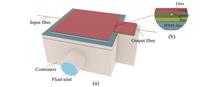
ObjectiveA variable optical attenuator is a key component for wavelength division multiplexing (WDM) transmission node power equalization, optical amplifier gain flattening, multiplexing point channel balancing, and receiving node power management in fiber optic communication. A fiber optic type variable optical attenuator has the advantages of simple structure, low insertion loss, low cost, and easy to interface with other optical fibers and waveguide structure, and is widely used. The adjustment accuracy and attenuation range are very important parameters of the variable optical attenuator, and there are few products with high adjustment accuracy and large attenuation range. In this paper, based on the traditional dislocation-type optical fiber variable optical attenuator with large dynamic range, the fluid pressure/pressure regulation is transformed into optical fiber micro-displacement control, which is easy to realize the micro-displacement precision control of optical fiber products to replace the high cost precision mechanical adjustment instrument of such products. In addition, the device meets the requirements of optical networks for attenuators, can work in a wide range of attenuation, and has low insertion loss and low wavelength-dependent loss, as well as compact structure,low cost, and high accuracy. According to the VOA optical power adjustment curve, film thickness can be selected to achieve configurable VOA optical attenuation accuracy.MethodsThe designed variable optical attenuator device is fabricated by ultra-precision processing technology. It contains components such as the polydimethylsiloxane (PDMS) elastic film, optical fiber carrying platform, and constant pressure pump. The adjustment of fluid pressure is transformed into micro-displacement control of the optical fiber by driving the ejection of the film through the fluid constant pressure pump, thus realizing the lateral dislocation of the docking fiber, and the optical attenuation is realized based on the dislocation of the ejected film driven by the fluid constant pressure pump and the docking fiber, while the adjustable accuracy of the optical intensity coupling efficiency is achieved by selecting the appropriate film thickness. We use the COMSOL Multiphysics software and three-dimensional finite difference time domain (FDTD) method to simulate and calculate the driving kinetic behavior and optical coupling efficiency of VOA, respectively. And in the experimental measurement stage, by replacing the film thickness of the device and adjusting the input pressure of the constant pressure pump, the trace mechanical dislocation and optical attenuation data are measured and the coupling efficiency is calculated, and then the relationship among the movement of the fiber-bearing platform, optical attenuation, and pressure control, and relationship between the wavelength-dependent loss and the optical attenuation of VOA with different film thickness and control pressure are derived. Finally, the relationship between the configuration of the film thickness and the precision of the variable optical attenuator is fitted numerically.Results and DiscussionsThe experimental results show that the variable attenuation range of this attenuator is greater than 60 dB (Fig. 3) with an insertion loss of 1.24 dB (Fig. 5) and a wavelength-dependent loss less than 1 dB (Fig. 6) under appropriate film thickness conditions. The variable optical attenuator is used for repeatability experiments at the wavelength of 1550 nm with satisfied performance. The response time of the device is less than 50 ms. In order to study the influence of film thicknesses on the regulation accuracy of the configured VOA, the film thicknesses are set to 0.3 mm, 0.4 mm, and 0.5 mm, and the pressure interval is 12.2 Pa. The accuracy of the VOA is measured, and the worst regulation accuracy of the VOA with film thicknesses of 0.3 mm, 0.4 mm, and 0.5 mm can be obtained when the dynamic range of the VOA is 10 dB. When the dynamic range of VOA is set equal to or greater than 40 dB, there is an inflection point for the change of the slope of the curve, and the worst adjustment accuracy of VOA can be taken as 0.16 dB, 0.15 dB, and 0.11 dB respectively near the inflection point. When the dynamic optical attenuation range of the variable optical attenuator is set to 10 dB and 40 dB, the adjustment accuracy is better than 0.04 dB and 0.11 dB for a film thickness of 0.5 mm, respectively (Fig. 7). The tuning accuracy will be higher when the film thickness increases.ConclusionsA variable optical attenuator with configurable adjustment accuracy is proposed to achieve transverse dislocation and optical attenuation of docked optical fibers by driving the film to pop up the fiber for lateral displacement. Both the numerical analysis and experimental measurement results show that the variable optical attenuator has an insertion loss of 1.24 dB, a return loss of -54 dB, a wavelength dependent loss of less than 1 dB, and a dynamic range of 60 dB. The thickness of the film of the device can affect the adjustment accuracy, and the relationship between the adjustment accuracy and the film thickness can be obtained by fitting the optical attenuation curve. This device can transform the adjustment of fluid pressure/pressure into precise control of transverse micro-displacement of fiber, which provides a new idea for the development of fiber optic products.
1) The differences in the system PM noise when the compensation interferometer and the sensor are adjacent and separated are analyzed theoretically. The results reveal that the amplitude difference in the system PM noise under the two structures is 20lg(τ2/τ).2) When the compensation interferometer is adjacent to the sensor, the PM noise and random noise on the transmission fiber can be greatly reduced by the optical differential effect. A smaller path-matched difference indicates a more significant optical differential effect, and the returned PM noise on the transmission fiber can be effectively suppressed.3) When the compensation interferometer is separated from the sensor, the PM noise is only related to the arm difference of the sensor, which is independent of that of the compensation interferometer or their optical path-matched difference. As the arm difference of the sensor grows, the PM noise also increases.4) The optimal PMDI structure is obtained. In the design of a remotely interrogated OFS system with internal modulation of PGC, the compensation interferometer should be well shielded from sound and vibration. When the requirements of the internal modulation of PGC and PM for arm differences are satisfied, the optical path-matched difference should be as small as possible. Meanwhile, the compensation interferometer should be adjacent to the sensor. The optical differential effect of this structure can be used to suppress the PM noise and low-frequency random noise on the transmission fiber.ObjectiveThe interferometric optical fiber sensing (OFS) system based on the beam interference principle has the advantages of a wide working frequency band, small volume, and invulnerability to electromagnetic interference. It is of great significance for national security, oil and natural gas exploration, seismic detection and warning, etc. The Mach-Zehnder and Michelson interferometer structures are commonly used in practical OFS systems. Among them, the OFS system with path-matched differential interference (PMDI) is one of the research hotspots for its simple structure, high optical energy utilization rate, and flexible demodulation schemes. Up to now, the interference of the conventional PMDI structure is usually perfectly matched, and the compensation interferometer is located at the emitter or receiver end. This structure has the following problems when it is applied to the remotely interrogated OFS system: 1) the pickup noise accumulates along the remote transmission fiber and will be finally converted into great system noise by the optical differential effect; 2) in the remotely interrogated OFS system, optical frequency modulation or phase modulation (PM) is required to suppress the phase noise induced by stimulated Brillouin scattering (SBS). As the interference of the conventional PMDI structure is usually perfectly matched, external carrier signals cannot be directly loaded into the interferometer, which means the conventional PMDI structure is no longer applicable. Although the carrier signals could be loaded on one arm of the interferometer by a piezoelectric transducer (PZT) or an electro-optic modulator (EOM), this will destroy the passive property of the system and also introduce some electrical noise. In view of the above-mentioned defects, the paper proposes an improved PMDI structure for remotely interrogated OFS applications. Through numerical simulation and experimental verification, the optimal PMDI structure for remotely interrogated OFS systems is obtained. We hope that the conclusions drawn in this paper can provide a theoretical and experimental reference for the comprehensive design and noise suppression of remotely interrogated OFS systems.MethodsThis paper studies the influence of the PMDI structure on the noise of a remotely interrogated OFS system with phase generated carrier (PGC) techniques. Firstly, the influence of different PMDI structures on PM noise is analyzed. Through numerical simulation and experimental verification, the optimal PMDI structure for the remotely interrogated OFS system is obtained. Then, the influence of different path-matched differences on the PM noise of the system is studied. Finally, the phase noise background with different optical path-matched differences is measured experimentally.Results and DiscussionsThe differences in the system PM noise when the compensation interferometer and the sensor are adjacent and separated are analyzed theoretically. The results show that the amplitude difference in the system PM noise under the two structures is . When the compensation interferometer is adjacent to the sensor, noise caused by environmental disturbance to the lead fiber can be greatly reduced by the optical differential effect (Fig. 2). When the compensation interferometer is separated from the sensor, the PM noise is only related to the OFS arm difference, which is independent of the arm difference of the compensation interferometer or their optical path-matched difference. When the OFS arm difference increases, the PM noise also rises (Fig. 3).ConclusionsThis paper first theoretically analyzes the influence of different structures and arm differences of the compensation interferometer and the sensor on the noise in the remotely OFS system of PMDI. Then, it designs an experiment for verification. The results show that the theory is in good agreement with the experiment, and the following conclusions are drawn.
Results and Discussions For the SMSP-MSF with a regular hexagonal lattice, with the increase in the diameter d11 of the gold-coated hole (Fig. 2) or the decrease in the thickness t of the gold layer (Fig. 4), the modal effective index of SPP mode increases gradually. With the increase in the diameter d11 of the gold-coated hole or that in the thickness t of the gold layer, the peak value on the loss curve for the x-polarized core mode increases first and then decreases (Fig. 3 and Fig. 5). After optimizing the structural parameters for each defect core and each gold-coated hole, six resonant wavelengths are evenly distributed in the whole interested band where the x-polarized core mode, defect core mode, and SPP mode resonate. The superposition of the six loss peaks forms a relatively flat and ultra-wide single-mode single-polarization transmission band. For the SMSP-MSF with a square lattice, the x-axis is the direction of the fast axis of the core but the slow axis of the defect cores. Even when the modal effective indexes of the x-polarized core mode and defect core mode have similar values, the difference between the modal refractive indexes of the y-polarized core mode and defect core mode is still very large. Therefore, the confinement loss ratio and polarization extinction ratio between the x-polarized and the y-polarized core modes are quite large in the whole interested wavelength range (Fig. 10).ObjectiveThe conventional single-mode single-polarization micro-structured fibers (SMSP-MSFs) achieve their SMSP property by coupling the unwanted polarized core mode to the cladding defect mode. This design method has contradicted the requirement on the number of air-hole layers outside the defect core, which further leads to the tradeoff between the confinement loss ratio Γ and polarization extinction ratio. In this paper, a novel kind of SMSP-MSFs based on a "coupling-coupling-absorption" mechanism is proposed for the first time to the best of our knowledge. In order to construct the proposed SMSP-MSFs, some gold-coated holes are introduced outside the cladding. The energy in unwanted polarized core mode is firstly transferred to the gold-coated areas through double coupling, namely, coupling from core to defect and coupling from defect to gold-coated area. Then, it is strongly absorbed in the gold-coated area by surface plasmon resonance. As a result, SMSP-MSFs with broadband single-mode single-polarization transmission can be achieved.MethodsBased on the above mechanisms, two broadband SMSP-MSFs are proposed. The first SMSP-MSF has a regular hexagonal lattice. The birefringence is introduced in the core by symmetrically enlarging two air holes around the core. In the cladding, air holes at the middle of every side of the fourth hexagonal air hole ring are reduced to different diameters to form six defect cladding cores. Besides, six air holes with different sizes are drilled outside the cladding, and then they are coated with a layer of gold of different thicknesses. By optimizing the structural parameters of the SMSP-MSF, the energy of the x-polarized core mode can be coupled to the gold's surface plasmon polariton (SPP) mode through the defect core mode at multiple wavelengths, due to the resonance among those modes. Then, the energy is strongly absorbed by the SPP mode, which results in a great increase in the lossof the x-polarized core mode. For this SMSP-MSF, the influences of the gold-coated hole's diameter and the gold layer's thickness on the position of the resonant wavelength and the confinement lossof the x-polarized core mode are studied respectively by the full vector finite element method. The second SMSP-MSF has a square lattice with one rectangular inner core and two rectangular defect cores. While the long sides of the core and the defect core are placed along the y and x axes, respectively, the directions of the fast axes of the core and the defect core are perpendicular to each other. When the modal effective index of the x-polarized core mode (which is its fast axis) is adjusted to have a similar value with that of the x-polarized defect core mode (which is its slow axis), the difference between the value of the modal effective indexes of the y-polarized core mode and y-polarized defect mode is still very large. This guarantees strong energy coupling between the core mode and defect mode in the x-polarized direction but very weak coupling between the core mode and defect mode in the y-polarized direction. After the energy in the x-polarized defect core mode is coupled to and absorbed by the SPP mode in the gold-coated air holes, an SMSP-MSF whose x-polarized core mode has large confinement loss but y-polarized core mode can transmit with low confinement loss can be achieved. For this SMSP-MSF, confinement losses for both polarized core modes are numerically computed around 1.55 μm by using the full vector finite element method. The modal field distribution of both polarized core modes is studied. The single-mode single-polarization bandwidth of this SMSP-MSF is analyzed.ConclusionsIn this paper, two novel ultra-broadband SMSP-MSFs are proposed for the first time based on mode coupling mechanism and surface plasmon resonance effect. The influences of the structural parameters of the SMSP-MSFs on both polarized modes' confinement loss are studied. For the SMSP-MSF with a regular hexagonal lattice, the coupling of x-polarized core mode, defect core mode, and SPP mode at multiple wavelengths is realized by introducing six different defect cores in the cladding and constructing six different gold-coated areas outside the cladding. The x-polarized core mode, defect core mode, and the SPP modes resonate simultaneously at 1.320 μm, 1.388 μm, 1.440 μm, 1.490 μm, 1.570 μm, and 1.640 μm. The energy in the x-polarized core mode is transferred out and absorbed by the SPP mode in a wide wavelength band efficiently. This results in an SMSP-MSF with a single-mode single-polarization wavelength band of larger than 380 nm. For the SMSP-MSF with a square lattice, the fast axis of the core and the defect core are perpendicular to each other. By this mechanism, strong coupling between the x-polarized core mode and x-polarized defect core mode, as well as weak coupling betweenthe y-polarized core mode and y-polarized defect core mode, can be achieved at the same time. After optimization of the structural parameters, the x-polarized core mode shows a confinement loss of 113.57 dB/m at 1.55 μm, while the y-polarized core mode's confinement loss is only 2.54×10⁻⁴ dB/m. The confinement loss ratio and polarization extinction ratio of the square-latticed SMSP-MSF can reach as high as 5×10⁵和113 dB, respectively. The two SMSP-MSFs proposed in this paper can be used in the areas of fiber sensors, fiber optic gyroscopes, in-line polarizers, coherent optical communication systems, etc.
Results and Discussions In this study, the neural network is trained and tested by selecting training and testing sets in four receiving planes with a height of 0 m, 0.5 m, 1.0 m, and 1.5 m, respectively, and the average errors of the four receiving heights are 1.01 cm, 1.14 cm, 1.36 cm, and 3.87 cm, respectively. The maximum positioning errors are 3.50 cm, 3.60 cm, 5.31 cm, and 12.79 cm, which can meet the demand for indoor positioning. Comparing the ISSA-ELM neural network positioning method proposed in this paper with the traditional three-sided measurement method, BP neural network, and that based on the L-M algorithm, the positioning accuracy is improved by more than 90%. At four different receiving planes with different heights, the ISSA-ELM neural network positioning method improves the positioning accuracy by 30.34%, 30.06%, 48.48%, and 45.42%, respectively, compared with the SSA-BP neural network, and it improves the positioning accuracy by 20.47%, 19.72%, 42.86%, and 42.32%, respectively, compared with the ELM neural network. The ISSA-ELM neural network positioning method shows great advantages in terms of positioning accuracy. By comparing the cumulative probability distribution of positioning errors of different methods, it is found that 90% of the positioning points of the positioning method proposed in this paper have an error of less than 7.32 cm, and the overall positioning error is significantly lower than that of other methods. In addition, the training time of the optimized ELM neural network using ISSA is only 0.0454 s, which is 35.14% lower than that of ELM, and thus the method has obvious advantages in terms of training time. The average positioning time of the ISSA-ELM neural network positioning method is 3.5 ms, which indicates a low positioning delay and meets the actual positioning requirements.ObjectiveWith the rapid development of the fifth-generation (5G) mobile communication and Internet of Things (IoT) technologies and the dramatic increase in the number of public indoor environments, research in the field of location estimation and tracking has shown great practical significance. The current mainstream global positioning system (GPS) and other various indoor wireless positioning technologies based on radio frequency communication cannot realize indoor precision positioning. Visible light communication (VLC) has attracted widespread attention from the academic community because of its performance advantages such as spectrum without authentication, high speed, environmental protection, energy saving, safety, economy. Therefore, visible light positioning technology has a broad application prospect. Specifically, the positioning method based on received signal strength indication (RSSI) is widely used for indoor visible light positioning with the advantages of high accuracy, low cost, and no clock synchronization. In recent years, research on machine learning (ML) and neural networks has developed rapidly, and various optimization algorithms and improvement schemes for indoor visible positioning have been proposed by integrating neural networks and RSSI positioning methods. Most of the previous studies on indoor visible light positioning based on neural networks only consider direct light and ignore the reflection of ceilings, walls, and indoor objects. In the actual environment, the existence of reflection will seriously affect the transmission of light signals and thus reduce the positioning accuracy, which cannot meet the actual needs when direct radiation is used to consider the positioning problem. At the same time, due to the difference in the distribution of light signals at different heights in the room, the height of a receiver will also directly affect the positioning accuracy and positioning error. In addition, the randomness of the initial weights and thresholds of the neural network can easily make the neural network fall into a local optimum. Using the intelligent search algorithm to determine the initial weights and thresholds of the neural network can both solve this problem well and accelerate the training speed of the network. In summary, this paper uses Circle chaotic mapping to improve the sparrow search algorithm (SSA) and optimize the extreme learning machine (ELM) neural network, and the paper proposes a positioning method combining ISSA-ELM neural network and RSSI based on Circle chaotic mapping optimization to achieve indoor visible light positioning with low latency and high accuracy. This method has taken into account the role of ceiling, wall, and ground reflections.MethodsThis study establishes an indoor visible light positioning model based on ISSA-ELM neural network and divides the positioning process into three stages. The first stage is the RSSI data acquisition stage, which establishes an indoor visible light positioning channel model based on the principle of VLC, arranges multiple LED light sources on the ceiling of the room, and uses multiple photoelectric detectors (PDs) in the receiving plane to receive and process RSSI signals from each LED light source respectively, and the real coordinates of the receiver are combined to determine the training set and test set of the neural network. The second stage is the neural network training stage. In this paper, we use an optimized ISSA based on Circle chaotic mapping optimization to determine the initial weights and thresholds of the ELM neural network, and the optimized SSA is not easy to fall into a local optimum and has a faster convergence speed. The neural network training uses the training set collected in the first stage, takes the RSSI data as the input of the neural network and the position coordinates corresponding to the PDs as the output of the neural network, trains the neural network, and establishes a prediction model for indoor visible light positioning. The third stage is the prediction model testing stage, in which the RSSI data are used as the input of the neural network using the test set selected in the first stage, and the predicted coordinates of the neural network are compared with the real coordinates of the test points, and the performance of the prediction model is evaluated using the positioning error and root mean square error function.ConclusionsIn this study, an ISSA-ELM neural network-based indoor visible light positioning method is proposed. The method firstly uses the ISSA algorithm to determine the initial weights and thresholds of the ELM neural network, which effectively avoids the problem of the weak generalization ability of the neural network brought by random initialization of weights and thresholds and speeds up the training speed of the ELM neural network to some extent. Secondly, considering the reflection of ceilings, walls, and floors inside the room, an indoor visible light positioning system based on the ISSA-ELM neural network is built. In a room of 5 m×5 m×3 m, it achieves low latency and high accuracy positioning with a neural network training time of 0.0454 s, average positioning time of 3.5 ms, and average positioning error of less than 4 cm. Finally, the ISSA-ELM method proposed in this paper is compared with seven other classical indoor visible light positioning methods. The results show that the positioning performance of the proposed method is superior, and the positioning error is reduced by 20.47%, 19.72%, 37.91%, and 42.32% in terms of four heights of 0 m, 0.5 m, 1.0 m, and 1.5 m, respectively, compared with the ELM neural network. The ISSA algorithm plays an obvious optimization role. In summary, the method proposed in this paper has fast positioning speed and high positioning accuracy, which can meet the positioning requirements of most indoor application scenarios.
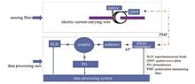
Results and Discussions Various optimization algorithms are compared and analyzed. When the energy spectrum entropy function is taken as the fitness function, the particle swarm optimization (PSO) algorithm has the best performance, but its time cost is too high. The grey wolf optimization (GWO) and HPO algorithms are the second best, and the HPO algorithm is better when the time cost and the iterations are taken into account. In this case, the HPO algorithm is better than the other optimization algorithms, as shown in Table 2. In addition, the main data processing methods are compared and discussed. When the signal-to-noise ratio (SNR), mean square error (MSE), and correlation coefficient are taken as the evaluation criterions, the OVMD-ICA has the highest SNR, the minimum MSE, and the largest correlation coefficient. The SNR should be greater than 30 dB according to the applicable standard of the electronic current transformer. The Wavelet (sym10), VMD-wavelet, and OVMD-ICA can suffice for the requirement, as shown in Table 3. The OVMD-ICA can achieve the optimal noise reduction effect, and the current resolution is 3 mA.ObjectiveThe fiber current sensor based on the Faraday effect and Ampère's circuital law can measure the current accurately. It has many advantages, such as excellent insulation characteristics, simultaneous measurement of the alternating current (AC) and direct current (DC), flexible sensor diameter, and digital output. However, it can hardly measure the microcurrent because the magnetic field generated by the weak current is small, and the Verdet constant of the sensing fiber is tiny (about 1 μrad/A when the wavelength is 1300 nm). Therefore, the current resolution of the fiber current sensor is limited. The methods to improve the current resolution mainly include the following: improving the optical path structure, increasing the number of optical fiber loop turns, and improving the Verdet constant of the sensing fiber. However, these methods have the disadvantages of complex operations and high costs. The data processing method is a promising scheme to improve the current resolution. To meet the requirements of information sources for independent component analysis (ICA) and improve the performance of variational mode decomposition (VMD) to deal with impact noise, this paper proposes the co-clustering algorithms of ICA and VMD with the parameters optimized by the hunter-prey optimization (HPO) algorithm.MethodsThis paper proposes the co-clustering algorithms of ICA and VMD with the parameters optimized by the HPO algorithm. Firstly, the random Gaussian noise, shot noise, impact noise, and output signal are measured. The output signal and noise characteristics of the fiber current sensor are analyzed. Secondly, the key parameters of VMD are optimized by the HPO algorithm. With the energy spectrum entropy function as the fitness function, the modal parameter K and the quadratic penalty factor α are obtained by the HPO algorithm, and VMD is realized with the two parameters. Third, the virtual channels of ICA are constructed. The mode functions are classified by the setting of the threshold of the correlation coefficient to construct the virtual channels for ICA. In this way, the application conditions of ICA are satisfied. Finally, the FastICA algorithm is applied for denoising.ConclusionsMore outstanding performance can be achieved in terms of the operation time, required iterations, and search for the globally optimal solution when the parameters of VMD are optimized by the HPO algorithm. The mode functions are classified by the setting of the threshold of the correlation coefficient to construct the virtual channels for ICA, and the FastICA algorithm is applied for denoising. The SNR of the output signal is enhanced, and the MSE is reduced by OVMD-ICA. By this algorithm, the SNR can be improved by at least 5 dB, and the resolution and measurement of 3 mA weak current can be realized.
Results and Discussions Firstly, to compensate for the shortage of quantization capability of fixed-resolution conventional images, the paper designs a photometric stereo-based image reconstruction method to achieve high-contrast normal mapping reconstruction of the blade surface at the image quantization level (Fig. 11). In addition, in terms of insufficient sampling descriptors for small defects, the multi-angle and multi-pose dataset is constructed from real blade images, and the loss function of the super-resolution model is improved by Charbonnier loss based on pixel loss. Additionally, the appropriate hyper-parameters are configured to reconstruct the high resolution and enhance the sampling resolution. The resolution-enhanced images can improve the original image pixel count to two to four times the original (Fig. 15), enhancing image details. Eventually, the super-resolution of small defects at both quantization and acquisition levels is enhanced (Fig. 19). The proposed enhanced reconstruction method finally uses the traditional Canny operator to identify the defect boundary of the blade surface. The experimental results show that the proposed method is immune to two-dimensional ambiguity and can improve the detection rate of minor defects on the metal blade surface by up to 24.3% (Table 5) compared to the traditional method.ObjectiveAiming at the difficulty of detection caused by low contrast and insufficient descriptors of micro defects in metal engine blades, this paper proposes a super-resolution image reconstruction technique to enhance micro defects. Various kinds of tiny defects may occur during the manufacturing and use process of metal aero-engine blades, which will have a huge impact on the appearance of the product or even the overall function. Therefore, the detection of tiny defects on the metal surface has profound significance for the overall product quality control and loss assessment of parts. Current detection methods are mostly based on manual detection, which has low reliability. The main factors that make it difficult to identify defects accurately are unclear feature boundaries and low contrast between defect contours and background, other noise in images or the two-dimensional ambiguity interference, and tiny defects with insufficient image descriptors for accurate identification. To address the above problems, researchers have proposed corresponding solutions from the perspective of image enhancement and fusion reconstruction. However, both image enhancement and image fusion methods start from the overall image information, such as adjusting the histogram, contrast, and other comprehensive attributes of the image to strengthen the features of the target, which are prone to problems such as negative optimization and two-dimensional ambiguity interference. Therefore, this paper performs image enhancement from the imaging principle and designs the image feature enhancement technique from the quantization and sampling aspects of image digitization respectively.Methods The image digitization includes two processessampling and quantization. With 8 bit grayscale images as examples, the discretization of the continuous coordinates of the image space is called sampling, and the grayscale values of some points, also called sampling points, in the space represent the image. The conversion of the grayscale values of the sampled pixels from analog to discrete quantities is called the quantization of the image grayscale, which determines the gray-level resolution of the image. The super-resolution quantization sampling enhancement technique for images of tiny defects on metal surfaces mainly focuses on contrast enhancement, resolution enhancement, elimination of two-dimensional illumination unevenness, and stain effects of tiny feature details of images. It can reveal low-contrast and border-unclear details in a way that can be more easily recognized by human eyes and computers while retaining the original clear features of images. In this paper, image enhancement is performed from the principle of imaging technology, and a two-dimensional super-resolution enhancement technique with fused image acquisition and quantization is designed. As the photometric stereo has the characteristics of refined normal mapping reconstruction, this paper proposes an image enhancement reconstruction technique based on photometric stereo and image hyper-segmentation to address the problems of existing methods. For the shortcomings of the quantization level in the digitization process, it uses photometric stereo technology for the high-contrast display to highlight the image contour features, overcoming the deficiency in the previous image with low contrast of fine features and vulnerability to two-dimensional ambiguity interference. For the deficiency of sampling resolution level in the image digitization process, the image hyper-segmentation reconstruction method is introduced to solve the problems of insufficient details and discrete image descriptors caused by the hardware bottleneck in the traditional photometric stereo technology.ConclusionsThe application of the image super-resolution reconstruction technique proposed in this paper can effectively improve the recognition rate of metal blade surface defects and reduce the false detection rate caused by two-dimensional ambiguity. The experimental results show that the recognition rate of minor defects on the metal blade surface can be improved by 24.3% compared with the traditional method. Especially in the case of stains on the blade surface and poor lighting effect of grayscale images, the image quantization contrast enhancement can shield the non-defective features such as stains and strengthen the display contrast of the surface, and the image sampling information enhancement can be pixel intensive and reduce the defects ignored due to too few pixels. The proposed method has a good prospect of application in industrial static inspection. Compared with the existing methods, the proposed method is applied in the image input preprocessing stage and can be easily integrated before the defect detection operator, which is conducive to promotion and popularization. Subsequently, it is possible to extend the applicability and improve the robustness of image fusion reconstruction with two-dimensional information enhancement by utilizing a streamlined and lightweight network to conduct targeted data training on detection objects and integrating the hardware structures of photometric stereo.
Results and Discussions The constructed 3D light-sheet microscopy imaging system based on the cooperation of the liquid zoom lens and the galvanometer mirror has good 3D imaging performance. As the drive current of the liquid zoom lens increases, the magnification of the system remains unchanged (Fig. 4). The displacement distance of the object-side principal plane has a linear relationship with the current applied to the liquid zoom lens (Fig. 5), and the axial position of the scanning light sheet has a linear relationship with the applied voltage of the galvanometer mirror (Fig. 6). For every 1 mV increase in the applied voltage of the galvanometer mirror, the liquid zoom is required. Specifically, when the applied voltage of the galvanometer mirror increases by 1 mV, the applied current of the liquid zoom lens needs to be increased by 1.73 mA. The position of the light sheet is moved by 3.00 μm, and the axial scanning range of the system, namely, the moving range of the object-side principal plane, can reach 507 μm (Fig. 7). The imaging experiments of fluorescent microspheres demonstrate that the lateral field of view of the system can reach 1970 μm×1300 μm (Fig. 9), and the actual detection field of view is 1970 μm×1300 μm×507 μm; the lateral resolution of the system is 1.32 μm, and the axial resolution is 12.75 μm (Fig. 10). The fluorescent microsphere samples are imaged by the 3D light-sheet microscopy imaging system to verify the correctness of the synchronous control timing of the liquid zoom lens, the galvanometer mirror, and the camera. The 3D reconstruction of the obtained light-sheet image is used to verify the feasibility of the system for 3D imaging of actual samples (Fig. 11). This paper employs the imaging of zebrafish embryos to verify the feasibility of the device for 3D imaging of thick biological samples (Figs. 12 and 13).ObjectiveWith the advancement of science, the research objects of life science have changed from monolayers of cells to organs and even in-situ measurement of animals. The study of biological samples relies heavily on three-dimensional (3D) volumetric imaging to provide structural and functional information about the samples. At present, there are mainly two methods to obtain the structure of biological tissue at different levels for 3D imaging of thick biological samples, i.e., the movement of samples and the simultaneous movement of the light sheet and the detection objective lens. The former can cause instability problems, while for the latter, the imaging speed is limited by inertia, and the magnification of the system changes during axial scanning. To capture the dynamic state of samples and avoid distortion of recorded data, we should ensure the volumetric imaging is performed in parallel at tremendously high speeds or by multiple planes sequentially, ideally without any sample movement. Therefore, we set up a 3D light-sheet microscopy imaging system based on the cooperation of the liquid zoom lens and the galvanometer mirror and design a synchronous control acquisition imaging system for the galvanometer mirror, the liquid zoom lens, and the camera to enable 3D imaging of the entire samples without sample movement. We use microspheres and zebrafish embryos to demonstrate the feasibility of the system to image thick biological samples. This study provides a feasible method for the 3D topographical observation of thick biological samples.MethodsIn this paper, we set up a 3D light-sheet microscopy imaging system based on the cooperation of the liquid zoom lens and the galvanometer mirror and design a synchronous control acquisition imaging system for the galvanometer mirror, the liquid zoom lens, and the camera. First, we use a double telecentric optical path as the imaging optical path, and thus the displacement of the principal plane of the system changes linearly with the focal length of the liquid zoom lens, while the magnification of the system remains constant. Then, we analyze the relationship between the power control range of the liquid zoom lens and the axial scanning range of the system and the relationship between the applied voltage of the galvanometer mirror and the scanning range of the light sheet. Next, the control timing relationship among the galvanometer mirror, the liquid zoom lens, and the camera is obtained by the imaging of the fluorescent microspheres. Afterward, the field of view and the resolution of the system are analyzed by the imaging of the standard fluorescent microsphere samples. Finally, the 3D imaging performance of the system is evaluated by the imaging results of microsphere samples and zebrafish embryos.ConclusionsWe set up a 3D light-sheet microscopy imaging system based on the cooperation of the liquid zoom lens and the galvanometer mirror and design a synchronous control acquisition imaging system of the galvanometer, the liquid zoom lens, and the camera. By the adjustment of the galvanometer mirror and the liquid zoom lens, the sample excitation by the light sheet is synchronized with the imaging to obtain the sample image stacks of different sections for 3D reconstruction and 3D imaging of the samples. When the imaging objective lens with a magnification of 10 and an NA of 0.3 is used, the axial scanning range of the system is 507 μm, and the lateral field of view reaches 1970 μm×1300 μm; the lateral resolution is 1.32 μm, and the axial resolution can reach 12.75 μm. The magnification of the imaging system remains constant during the axial scanning process, which can meet the requirements of the imaging experiments and related studies of a certain size of biological samples, and the imaging of zebrafish embryos demonstrates the imaging feasibility of thick biological samples. It is expected that liquid zoom lenses with larger apertures and better focusing performance will emerge soon, and with high-speed cameras, high-speed volumetric imaging of large biological samples can be achieved, or with line scanning for the suppression of sample scattering, the imaging performance of large biological samples can be improved.
Results and Discussions Ten repeated experiments are carried out to validate the subnano-scale measurement method. The piezoelectric ceramics nanopositioner is used for unidirectional scanning at an interval of 50 nm for 10 scans. The mean of the displacement measurements for the 10 sets of data is 50.0254 nm, with a standard deviation of 0.114 nm, which demonstrates that the proposed method can achieve subnano-scale precision displacement measurement. Moreover, 40 validation experiments are performed for 10 μm and 30 μm displacements separately to validate the method over a large measurement range. For the 10 μm displacement, the results display a mean of 10.0149 μm, with an average relative error of 1.577% and a standard deviation of 0.2040 μm. In the case of the 30 μm displacement, the mean is 30.0057 μm, with an average relative error of 0.368% and a standard deviation of 0.1453 μm. It is proved that the proposed method can achieve precision displacement measurement over a large range. Simulations are carried out to validate the aberration correction scheme based on the differential evolution algorithm. For a standard displacement of 30 nm, the displacement measurements before and after correction are 32.033 nm and 30.332 nm, with relative errors of 6.78% and 1.11%, respectively. The results demonstrate the effectiveness of the correction method.ObjectiveAccurate precision displacement measurement systems are of great importance to the revolution in human scientific research and the iterative upgrade of industrial manufacturing. The research on vortex beams is developing rapidly, with promising applications. The vortex beam has a spiral phase, and each photon of the beam carries orbital angular momentum. With the continuous improvement of the production and detection technology for vortex beams, the research on their applications in precision displacement measurement has been on the increase. In this study, to address the contradictory problems of a large range and high accuracy in precision displacement measurement, a precision displacement measurement system with interference of conjugated vortex beams is designed and built. It is expected that this solution can provide new research ideas and technical ways for high-accuracy and large-range displacement measurement, which is of positive significance to the development of contemporary science, technology, and industry.MethodsA precision displacement measurement method based on the interference of conjugated vortex beams is proposed in this study, with the interference pattern of conjugated vortex beams as the source of displacement data. By establishing the mathematical relationship between rotational angle radian of the pattern and displacement and designing the experimental data processing algorithm for subnano-scale displacement and large-measurement-range displacement, accurate precision displacement measurement results can be obtained by accurate extraction of the rotational angle radians. Then, an optical system is designed and simulated according to the modified Mach-Zehnder structure for the measurement scheme (Fig. 5). An experimental system is developed and experimentally tested to verify the effectiveness of the proposed method (Fig. 6). In addition, aberrations in the optical system can be corrected by differential evolution algorithms to improve the accuracy of the displacement measurement system.ConclusionsIn this study, a new precision displacement measurement method is established on the basis of interference of conjugated vortex beams. The interference pattern of conjugated vortex beams is used as the source of displacement data, and a mathematical relationship between rotational angle radian of the pattern and displacement is established. An optical design is carried out, an experimental system is set up, and the proposed method is validated. The results of the 10 sets of experimental measurements demonstrate a mean of 50.0254 nm, with a standard deviation of 0.114 nm at a displacement of 50 nm, which indicates the validity of the proposed method. Meanwhile, the proposed experimental system can also perform precision displacement measurements over a large measurement range, and the experimental results show that the proposed method can be used for a measurement range of at least 30 μm. In addition, the system aberrations in the vortex beam interference process are fitted, and the measurement accuracy of the proposed method can be improved by reasonable compensation of the optical system. The proposed system renders a new research idea and technical approach for displacement measurement with high accuracy and a large range, and provides the basic theoretical and technical support for precision displacement measurement in fields such as lathe processing, the semiconductor industry, and aerospace.
Results and Discussions For N-step PSP, M-coded (in this paper, M=3) patterns can mark NM fringe orders, which can effectively improve the number of fringe orders. In this paper, four conventional sinusoidal phase-shifting patterns provide a high-quality wrapped phase, and three quasi-sinusoidal coded patterns can be used to extract the corresponding fringe order map independently. The results (Table 1) of several planes with known heights show that the reconstructed planes with different heights are very close to the corresponding standard planes, which verifies that the proposed temporal phase unwrapping method can accurately obtain the corresponding fringe orders of wrapped phases. To obtain fringe orders, both Gray-code and phase-code methods require rounding operation, which generates round-off errors. Overall, the existing stair-shaped codes have high sensitivity and great difficulty in determining numerous fringe orders due to complex shapes or texture variations. Facing complex surfaces with a large range of reflectivity, the proposed N-ary sinusoidal codewords are considerably self-adaptable to non-uniform reflectivity due to the loose quantification processing. The analysis of theory and experimental results indicates that the proposed coding method has higher coding efficiency and robustness than intensity-code methods, and is more flexible and concise than phase-code methods while breaking the limitation of the total number of fringe orders to recover the absolute phase more accurately. The validity and superiority of the proposed method are confirmed by experiments.ObjectivePhase-shifting profilometry (PSP) has been widely used in various three-dimensional (3D) scenes due to its high accuracy and robustness. In fringe projection profilometry (FPP), unwrapping the phase map in (-π, π] is an inevitable consideration. Phase unwrapping algorithms are commonly divided into two types: spatial phase unwrapping algorithms (SPUAs) and temporal phase unwrapping algorithms (TPUAs). Conventionally, TPUAs are more suitable for measuring discontinuous objects as they can identify fringe orders pixel by pixel. TPUAs are also employed in real-time 3D measurement because of the development of hardware and defocusing systems. Numerous TPUAs have developed at a fast pace in the past few decades, mainly including multi-frequency, intensity-code, and phase-code ones. Multi-frequency methods suffer the low accuracy of the low-frequency patterns and the complicated selection among different frequencies. Intensity-code methods, mainly N-ary Gray codes with concision and high efficiency, directly use intensity information to generate the fringe order map, but they can barely measure colorful objects. In phase-code methods, massive codewords are coded into the phase domain with a depth of only 2π, and the difference between adjacent quantized phases may be too small to ensure the correct decoded codewords for a large number of fringe orders. Essentially, the proposed sinusoidal codewords are directly extracted from N-step phase-shifting patterns to replace additional stair-shaped codewords in intensity-code and phase-code methods. By contrast, the proposed fringe-order encoding method based on N-ary sinusoidal codewords performs outstanding coding flexibility and efficiency while breaking through the limitations of the number of fringe orders in phase-code methods and overcoming the sensitivity to reflectivity in Gray-code methods.MethodsA temporal phase unwrapping method based on N-ary coding is proposed to realize the 3D measurement of colorfully complex objects. When measuring an object with a large range of overall surface reflectivity, traditional stair-shaped patterns face the difficulty of quantization of an excessive number of fringe orders. During encoding, N-ary sinusoidal codewords are successively extracted from sinusoidal phase-shifting patterns to replace traditional quantized gray codewords. It is worth noting that the edges of the extracted N-ary codewords coincide with the 2π discontinuities of wrapped phases to reduce the mismatch. By numeral system conversion, N-ary sinusoidal codewords are embedded into different periods of projected patterns to achieve the encoding of fringe orders. During decoding, the differences between coded patterns and N-step sinusoidal phase-shifting patterns can be first used to calculate N-ary quantized patterns by a loose operation [Eq. (5)], and then a unique fringe order can be obtained by reverse numeral system conversion. To remove the mismatches caused by the defocusing and noise of the system, a fringe-order self-correction method [Eq. (10)] is used to correct the jump errors around the 2π discontinuities of wrapped phases. Finally, the absolute phase can be obtained by the collation of the corrected fringe orders and wrapped phases. In this paper, an object [Fig. 5 (a)] with several planes of known height is measured to verify the feasibility of the proposed method, and some colorfully complex scenes [Figs. 8 (a)-(c)] in our daily life are further measured to demonstrate its high performance.ConclusionsA temporal phase unwrapping method based on N-ary coding is proposed. By extracting the codewords from phase-shifting patterns to replace additional stair-shaped codewords in the existing TPUAs, the proposed method makes encoding and decoding more flexible and efficient. The experimental results demonstrate that the proposed self-coding method features high robustness for measuring sharply discontinuous and colorful objects in practice.
Results and Discussions The multifunctional Stokes-Mueller polarimeter based on embedded phase sensing is applied to the measurement of a lung cancer tissue section. 10 positions are selected from the normal and malignant areas for polarization and phase measurement, respectively. The results show that the morphology and arrangement of cells in different areas are not the same. In the malignant area, the arrangement of cells is disorderly, and the number of cells increases exceptionally due to excessive proliferation. Quantitative analysis shows that the depolarization and absolute-phase values of the malignant area are both large. That is, normal and malignant tissues have different refractive indexes, and this is crucial for optical diagnosis (Figs. 5 and 6). The malignant area has more cells than the normal area, and it also has a depolarization value higher than that of the normal area in both the whole image and a single cell (Table 1). The refractive index values of the cells in the malignant area measured at the wavelengths of 600, 633, and 700 nm are all larger than those of the cells in the normal area. To be precise, the refractive index values of the cells in the normal area measured at the three wavelengths are 1.383, 1.384, and 1.377, respectively, while those of the cells in the malignant area are 1.518, 1.516, and 1.511, respectively (Table 2). Therefore, depolarization parameters of polarization decomposition and the refractive index derived from the absolute phase can be used to determine whether a tissue is abnormal or early cancerous.ObjectiveSince polarization imaging technology can extract richer structural and optical information of samples and is highly sensitive to changes in subwavelength microstructures, it has a bright application prospect in biomedicine. The Mueller matrix has been widely used in the pathological diagnosis of cancers because it can quantitatively provide complete polarization information of biomedical specimens. However, the existing Mueller imaging polarimeter loses the absolute phase information of the sample, and the relative phase information cannot reflect the change law of the phase to be measured. Absolute phase, as a basic property of light, quantifies the phase characteristics determined by the physical thickness and refractive index coefficient of the sample and reflects the changes to be measured. As one of the most important optical properties of biological samples, the refractive index has been proven to be useful for describing the optical properties of biological tissues and evaluating pathological tissues. As an absolute-phase detection method, the quadriwave lateral shearing interferometer is highly suitable for phase microscopic imaging and the measurement of absolute phase information of samples due to its advantages, such as no need for additional wavefront reference beam, no special requirements on the light source, and simple structure. However, the applications of the quadriwave lateral shearing interferometer in the pathological diagnosis of cancer tissues are rarely reported. Therefore, an embedded absolute-phase detection instrument needs to be developed to meet the detection requirements of different types of samples.MethodsAs the existing Mueller imaging polarimeter loses the absolute phase information of the sample, a multifunctional Stokes-Mueller polarimeter based on embedded phase sensing is built. Specifically, the analysis of the polar decomposition equation for the Mueller matrix shows that the Mueller matrix does not retain the absolute phase information of the polarized light, but only contains the phase delay information of polarized light. Then, the self-developed quadriwave lateral shearing interferometer is integrated into the polarimeter. A multifunctional Stokes-Mueller polarimeter based on embedded phase sensing is thereby obtained, and it solves the problem of missing absolute phase in the measurement results obtained by the Mueller matrix polarizer. Finally, the phase distribution of the sample is reconstructed by MATLAB according to the collected interferogram, and the refractive index is calculated. With a lung cancer tissue section as the research object, in addition to the extraction of polarization information of the biological sample, the refractive index is measured on the basis of the absolute-phase value. This instrument can serve as a new quantitative diagnostic index and enrich the measurement function of the polarizer.ConclusionsThe multifunctional Stokes-Mueller polarimeter based on embedded phase sensing solves the problem of missing absolute phase in the measurement results obtained by the Mueller matrix polarizer. The refractive index of the sample is measured on the basis of the absolute phase, and it can serve as a new quantitative diagnostic index for cancer diagnosis. An experiment is conducted with a lung cancer tissue section as the research object, and the results show that the depolarization parameter and refractive index of the malignant area are all larger than those of the normal area. The distinction between the normal and malignant areas can thus be achieved. The developed instrument can not only extract polarization parameter, but also quantify the refractive index information of the tissue. In this way, it further expands the functions of the traditional Mueller polarimetric imager. The combination of polarization information and phase information can provide a more comprehensive quantitative evaluation index for cancer diagnosis. In the future, this instrument can assist researchers in the preliminary screening of indicators, which reflects the application potential of the proposed instrument in pathological diagnosis research.
Results and Discussions In order to verify the accuracy of the proposed measurement method, a semi-physical simulation test is carried out in the laboratory by using a high-precision two-dimensional rotating platform to simulate the rotating device of the artillery, and a field test is carried out in a artillery factory. Both semi-physical simulation test and field test have verified the measurement accuracy and repeatability deviation of the measurement system. The semi-physical test results show that the measurement accuracy of barrel altitude angle is better than 0.09° [Fig. 5(a)], and that of direction angle is better than 0.15° [Fig. 5(b)]. The repeatability deviation of both angles is better than 0.0035° (Fig. 6). The field test results show that the measurement accuracy of the measurement system for altitude angle is better than 0.15° (Table 1), while that for direction angle is better than 0.12° (Table 1), and the repeatability deviation of both angles is better than 0.0035° (Fig. 9). The field test results are basically consistent to those of semi-physical simulation test, and the repeatability deviation is very low, which shows that the measurement method is highly robust to external disturbances such as light instability.ObjectiveThe artillery adjustment accuracy directly affects the hitting accuracy of the artillery, and it is a key performance parameter of the artillery. The system deviation of a fire control system before artillery equipment or after serving for a period of time is generally large, which results in a large deviation between the actual direction of the barrel and the setting direction of the system. The accuracy of artillery adjustment can be evaluated by using high-precision barrel pointing measurement, and the system deviation of the fire control system can be corrected by using pointing measurement data to improve the hitting accuracy. At present, the double theodolite method is widely used for barrel pointing measurement. The theodolite needs to acquire the horizontal angle and zenith angle data of observation points in the form of artificial sighting, and the measured data need to be manually input into the computer to calculate the barrel pointing. The low measurement efficiency and low degree of automation restrict the production efficiency of the artillery, and it is difficult to meet the rapid calibration requirement of the fire control system in future battlefield environments.MethodsThe visual measurement method features non-contact, speediness, high accuracy, and easy integration. In this paper, a new method of barrel pointing measurement based on binocular vision is proposed. With corner points of a chess board fixed on the barrel as cooperative marking points, images taken by two cameras when the barrel is at zero position and measuring position are automatically analyzed by image processing, and the pixel coordinates of cooperative marking points in the images taken by two cameras are calculated and used to analyze barrel rotation. It is proposed to decompose the rotation of the barrel into two revolving movements, with only the direction angle and altitude angle changing, respectively. On this basis, measurement equations are established, and the direction angle and altitude angle are decoupled. The direction quantity of the plumb line in the camera coordinate system is obtained by plumb line measurement, and the relationship between the camera coordinate system and the geodetic coordinate system is established, with the initial value of the barrel in the geodetic coordinate system obtained. Then, LM (Levenberg-Marquardt) algorithm is used to optimize the barrel pointing, and the final result of barrel pointing is obtained.ConclusionsIn this paper, an artillery barrel pointing measurement system based on binocular vision is built, and measurement equations are derived. The measurement system software is developed, and the functions of system calibration and measurement are integrated to realize automatic measurement. The introduction of plumb line in the measurement method brings the advantage of low operation difficulty compared with the existing visual measurement methods and improves the convenience of visual measurement methods in the application of barrel pointing measurement. Barrel pointing measurement can be accomplished when the cooperative marking points are arranged arbitrarily without installation error calibration. The semi-physical test and field test results prove that the method presented in this paper has the advantages of high measurement accuracy, high robustness, and full-automation. It provides a new scheme for the pointing measurement of artillery barrel, which can realize the automatic measurement of artillery barrel pointing in future battlefield environments and has broad application prospects.
Results and Discussions Specifically, the microscopic images of six typical types of pixels are presented (Fig. 4). To prevent the problems of low detection accuracy, low goodness of fit, and poor robustness of the detection model resulting from insufficient samples of inkjet-printed OLED pixels, this paper extends the number of initial samples collected by a data augmentation algorithm (Fig. 5). The sample datasets are built (Table 1), and the defects in the inkjet-printed OLED pixel images with defects of different types are detected. According to the results, the method proposed in this paper performs best in detecting two types of defects, namely, single-class satellite points, and failures to cover the whole bank. It delivers the second-best results in detecting the overflow of overlarge ink droplets from the bank and the mix of multiple types of defects (Table 2). Subsequently, the paper compares the defect detection area under the curve (AUC) values of the proposed method and the current unsupervised defect detection methods based on feature space, i.e., semantic pyramid anomaly detection (SPADE) and patch distribution modeling (PaDiM), on the inkjet-printed OLED pixel image dataset. Then, taking the single-class satellite points as an example, this paper compares the effectiveness of different methods in defect segmentation on the inkjet-printed OLED pixel image dataset (Fig. 6). By contrast, the performance of SPADE algorithm severely degrades, and this is caused by the lack of customized feature learning. The model proposed in this paper can capture the feature distribution of defect-free images well in a small amount of data, indicating the effectiveness of the proposed method in detecting inkjet-printed OLED pixel defects.ObjectivePreparing organic light-emitting diode (OLED) displays by inkjet printing technology is a research direction for next-generation display technologies. This technology is a material-saving deposition technology characterized by simple process, low cost, low power consumption, and capability for mass production, and it has thus been widely used in the electronics industry. The inkjet printing process imposes an extremely strict requirement on the accuracy of the process parameters, and printing defects are prone to occur when the parameters are outside the error ranges. In the preparation process, the printed OLED pixel image consists of repetitive and equally spaced horizontal and vertical lines, and this background texture varies with illumination conditions. The variation in texture, the low contrast of the defective pixels, and the changing size of the defective area pose a great challenge to the detection of printing defects. The possible printing defects are divided into two main categories: film-forming integrity defects in printed OLED pixels and film thickness uniformity defects in printed OLED pixels. Among them, film-forming integrity defects include the presence of satellite points, failure to cover the whole bank, overflow of overlarge ink droplets from the bank, and a mix of multiple types of defects. Automatic optical inspection (AOI) technology is widely used for the detection of OLED defects. Although most of the existing methods achieve favorable results in detecting the defects on the OLED panel surface, they tend to ignore the detailed features of defects in printed OLED pixels when they are applied to detect such defects. They are insufficient in the cases of limited printed pixel images and tiny pixel defects and consequently fail to deliver favorable results in pixel defect detection when the quality of printed OLED pixel images is reduced. To effectively improve the accuracy of the detection of OLED pixel defects and achieve the intelligent detection of inkjet-printed OLED pixel defects, this paper proposes an extended feature pyramid network (FPN) and applies it to the task of detecting OLED pixel defects.MethodsThe features are enhanced by fusing the feature pyramids at different levels. A dedicated feature extraction module for small targets is added to enhance the sensitivity of the detection of OLED pixel defects. Then, an additional high-resolution pyramid layer is used to extract credible regional details, and the channel capacity is reduced by fusing the two pyramid layers at bottom to fully utilize the information from the underlying feature map. Finally, transfer learning is applied to limited samples to address the problem of low goodness of fit caused by insufficient sample data.ConclusionsThis paper proposes a detection method for OLED pixel defects based on an extended FPN. According to the features of inkjet-printed OLED pixel defects, the paper extends the original FPN, effectively obtains regional details at different levels of the hierarchy, and integrates semantic information from higher levels in a pyramidal manner to enrich the underlying features and enhance the contrast of details. More accurate detection of OLED pixel defects is thereby achieved. In addition, combined with ResNet18, the method proposed in this paper attains a robust generalization ability for a limited amount of OLED pixel image data. The results show that compared with other methods, the proposed method demonstrates superior performance, with a defect detection rate of 99.8% and a defect segmentation accuracy of 88.8% on the inkjet-printed OLED pixel dataset. Therefore, the proposed method can achieve favorable detection results on such small sample datasets and largely meets the industrial demand of OLED mass production in large sizes.
Results and Discussions A strategy is proposed to eliminate the phase ambiguity of the twin-Fock state. Numerical simulation results verify that the strategy can eliminate phase ambiguity, and the phase sensitivity of the fluctuation of the estimator is better than the standard quantum limit in the whole phase interval. The main work is as follows: firstly, based on the related literature, the numerical simulation of the coincidence count measurement of the twin-Fock state light source and the single-photon light source in the Mach-Zehnder interferometer is carried out. Then the measurement strategy proposed in this paper is simulated, and the effectiveness of the simulation results is analyzed. Finally, the reduction sensitivity of the measurement strategy is given, and the whole phase interval is sampled to obtain statistical data. Furthermore, the unbiasedness of the estimator is verified numerically. The standard deviation of the measurement is compared with the theoretical expectation, the standard quantum limit, and the Heisenberg limit. The maximum likelihood estimation of the multi-output method for the twin-Fock state without bias phase was previously available, and it can be found that its likelihood function has two maximum points in a phase period. In this paper, we propose that when using multi-output measurement and maximum likelihood estimation, there is only one maximum point in a phase period if we combine the measurement results with the bias phase and without the bias phase to obtain the joint likelihood function. This paper gives an analysis of this phenomenon based on the approximation of linear combination estimators of maximum likelihood estimators. By generalizing the joint likelihood function measurement method of binary-outcome measurements to the multiple-output case, we find that it is possible to reduce the phase estimator from 4 to 2 in using only the twin-Fock state. Through the relationship between the maximum likelihood estimator and the inverse function estimator in the case of multiple outputs [Eqs. (9)-(14)], we have semi-analytically explained the reason why this method works. We then use the single-photon state for joint measurement, which ultimately eliminates phase ambiguity. Using the Monte Carlo method, we simulate the measurement process, and the results have validated our analysis results (Fig. 3). Finally, we calculate the Fisher information and the Cramer-Rao lower bound (CRB) of our measurement scheme as the analytical analysis of phase sensitivity. The numerical simulation results (Fig. 4) show that our estimator can beat the standard quantum limit.ObjectiveMetrics play a central role in science and engineering. It is concerned with the final reachable accuracy of parameters or phase estimation and the construction of measurement schemes to achieve this accuracy. By combining quantum mechanics and basic theories of statistics, quantum metrics find that the final lower limit of estimation accuracy is related to input state preparation, phase accumulation modes, and measurement schemes, and the main goal is to break through the standard quantum limit and reach the Heisenberg limit of measurement accuracy. In recent years, due to the progress of experimental conditions, quantum metrics have been widely used in the frontier fields such as gravitational wave detection and atomic clocks. A major research direction of quantum metrics is phase estimation in optical interferometers, which was first proposed in research on the input coherent light and compressed light in Mach-Zende interferometers by Caves et al., and its theoretical phase sensitivity can reach the physical limit (Heisenberg limit). In recent years, other kinds of non-classical light sources have also been studied, such as the NOON state and twin-Fock state. The NOON state is a numerical light source that can theoretically reach the Heisenberg limit, while the twin-Fock state has theoretical phase sensitivity up to the Heisenberg scale and is more robust to photon loss than the NOON state. However, coincidence count detection for the twin-Fock state results in a multi-peak structure of the phase distribution (i.e., the likelihood function), which is the so-called phase ambiguity. Aiming at this problem, we propose a simple scheme to eliminate phase ambiguity and analyze its performance.MethodsA binary-outcome photon counting and joint likelihood function measurement are employed in this work, where the detection event with an equal number of photons is a measurement outcome. All the other detection events are treated as another outcome. We generalize it to a multi-output scenario and use single-photon states for joint measurement. According to the relationship between the maximum likelihood estimator and the inverse function estimator in the case of multiple outputs, we have semi-analytically explained the reason why this method works. Using the Monte Carlo method, we simulate the measurement probabilities of the six-photon twin-Fock state and the single-photon state and get a numerical simulation of the measurement scheme, where the experimental imperfection is added artificially.ConclusionsWe propose a simple scheme to eliminate phase ambiguity of coincidence count detection for the twin-Fock state. Our scheme relies on a sequence of the N-photons Fock states and the single-photon state that are injected into the interferometer to realize a single-peak structure of the total phase distribution, which determines the maximum likelihood estimator. Phase uncertainty of the estimator can beat the standard quantum limit over the entire phase interval.
Results and Discussions With a hollow hexagonal aluminum bar as the research object, the proposed method is used to conduct 3D reconstruction and thermal deformation research (Fig. 4). In the 3D reconstruction experiment, the maximum reconstruction deviation between the reconstructed surface and the fitted surface is about 0.004 mm, and it is mainly concentrated in the splicing area, while the deviation in other areas is relatively stable. The stereo reconstruction angle also proves that the system has stable performance and high accuracy (Fig. 6). In the thermal deformation research experiment, the proposed method can be used to obtain the average height of the first and last frame images in the vertical direction of the B and C surfaces of the part, respectively (Table 1). It can be seen that the maximum change in the height of surface B of the part is 0.5467 mm, and that of surface C is 0.5589 mm (Fig. 7). Then, the height change of surface A of the part processed by the system are directly compared with that of surfaces B and C processed by the proposed method during the cooling process, and comparison is carried out every 30 frames from frame 0 to 1290. There are 44 frames of comparison images (Fig. 8). Finally, the finite element analysis software ANSYS is used to simulate the part, and the steady-state simulation is selected. The temperature of the part rises from 20 ℃ to 310 ℃ in simulation experiments. It can be seen that the maximum thermal deformation of the part in the vertical direction is 0.5500 mm, which indicates that the thermal deformation of the part along the z direction is 550.0 μM when the temperature difference is 290 ℃ [Fig. 9 (b)].ObjectiveThe application of digital image correlation (DIC) technology is very extensive, and the technology has high practical value in biotechnology, civil engineering, aerospace, medical application, and other fields. With the continuous advancement of related technologies, the demand for full-field deformation measurement and 3D shape reconstruction of objects has increased accordingly. This requires the DIC technology to not only have higher measurement accuracy but also be more economical and practical, so as to make itself be applied to more fields. In recent years, many scholars have done a lot of research on the full field strain and deformation measurement by DIC, and they have made many valuable research results. Among them, the multi-camera DIC system has been proven to have high measurement accuracy, and it is feasible to achieve full field or double surface deformation measurement. However, in actual use, the system takes a long time to be built and involves a complex operation and high economic costs, and there is interference between multiple cameras. The rotation of a single camera is used to realize the full field deformation measurement of the measured object under different load conditions. In other words, the camera is continuously moved to rotate around the same measured object, and it will shoot and record in multiple different positions, so as to finally cover all the required fields of view. The system has low cost, complex operation, and low accuracy. In view of the problem that a monocular camera is difficult to be used in full-field deformation measurement and the complexity of multiple cameras in full-field deformation measurement, a new method of full-field deformation measurement by using a double-sided mirror-assisted dual-camera system is proposed.MethodsThis research adopts a coordinate transformation method based on camera calibration. In other words, the transformation from the real camera coordinate system to the virtual camera coordinate system is realized through the double-sided mirror, and then the transformation from the real object to the virtual image is realized. It is assumed that the camera coordinate system of L coincides with the world coordinate system of the binocular DIC system (Fig. 3). Therefore, the conversion relationship between the world coordinate system of the virtual binocular DIC system and that of the real binocular DIC system is equivalent to the conversion relationship between the camera coordinate systems of L′ and L. First, it is necessary to find out the positional relationship between the coordinate system oc-xcyczc and the O1-X1Y1Z1. The rotation and translation matrices between the camera coordinate system oc-xcyczc and O1-X1Y1Z1 can be obtained through camera calibration. Then, an intermediate coordinate system is introduced, namely, the coordinate system O2-X2Y2Z2, which is a rotating coordinate system of O1-X1Y1Z1. According to the imaging law of the plane mirror and the nature of the Euler angle, the rotation and translation matrices from the coordinate system ov-xvyvzv to the coordinate system O2-X2Y2Z2 can be obtained, and then the rotation and translation matrices from the coordinate system ov-xvyvzv to the coordinate system O1-X1Y1Z1 can be obtained. Finally, the conversion relationship between the real camera coordinate system and the virtual camera coordinate system can be calculated by synthesizing the above results.ConclusionsA new method of full field deformation measurement using a double-sided mirror-assisted binocular DIC system is proposed. With a hollow hexagonal aluminum bar as the measuring object, the thermal deformation results of three outer surfaces are measured during the cooling process from 310 ℃ to 20 ℃, and they are compared with the simulation results of the finite element software. The results show that the change curves of the three outer surfaces of the part along the height direction basically coincide with the simulation results, and the absolute error between the calculated average thermal deformation values of A, B, and C surfaces along the height direction of the part by using the proposed method and the simulation results is 2.8 μm. The relative error is only 0.51%. It can be seen that the proposed method not only overcomes the limitation that a monocular camera cannot realize full field measurement but also discards the complexity of a multi-camera DIC system.
Results and Discussions The light absorption intensity of the all-fiber capacitive device based on the GO/PS composite increases with the driving voltage [Fig. 5 (a)], which indicates that the absorption characteristics of the device can be effectively adjusted by the electrical field. The feasibility of the experiment is also verified. To further observe the difference in the optical transmission efficiency of the device under positive and negative voltages, the variation in the optical transmission capability of the device with the driving voltage under a low pump power (35 mW) is tested [Fig. 5 (b)]. The results show that the device achieves higher modulation efficiency under the positive voltage due to the properties of n-type semiconductors caused by slight doping. The nonlinear optical absorption characteristics of the GO in the modulator can be adjusted by the driving voltage, and the intracavity loss can thereby be modified. On this basis, the variation of the insertion loss of the GO/PS modulator is studied when the driving voltage increases from -60 V to 60 V. As the positive bias voltage reaches up to 20 V, the insertion loss of the device is reduced from 2.30 dB to 0.86 dB [Fig. 7 (b)]. Then, the device is applied to the all-fiber mode-locked ring laser system (Fig. 6). The results show that the laser achieves the switching among three operating modes: continuous wave, Q-switched mode locking and continuous wave mode locking under a certain range of the modulation voltage (a range from 0 V to 20 V). This all-fiber electro-optic modulator also reduces the pulse width of the mode-locked signal to 20 ps. Radio-frequency (RF) spectral measurements are conducted to characterize the stability of the fiber laser. The RF spectra of the mode-locked laser are measured [Fig. 9(d)]. The signal-to-noise ratio (SNR) of the RF signal can reach up to around 60 dB at 21.40 MHz. To further verify the stability of the laser, the average output power of the laser in 180 minutes is measured (Fig. 10). According to the results, the all-fiber mode-locked ring laser based on the GO/PS electro-optic modulator can work steadily for a long time.ObjectiveShort-pulse fiber lasers have attracted great interest in numerous fields, including fiber communication, laser medical treatment, bioengineering, and material processing, owing to their compact structure, high efficiency, and robust stability. Physically, mode locking is an effective method to obtain ultrashort pulses, and it can be divided into active mode locking and passive mode locking. Passive mode locking based on saturable absorbers (SAs) has been widely studied. Among the SA materials, two-dimensional (2D) materials, such as graphene, black phosphorus, and molybdenum disulfide (MoS2), are promising candidates due to their distinctive nonlinear saturable absorption ability, ultrafast recovery rate, and low cost. Plenty of passively mode-locked fiber lasers based on 2D materials have been developed to achieve different operating modes, such as continuous wave, Q-switched mode locking, and continuous wave mode locking by changing the pump power. However, due to the relatively fixed optical absorption characteristics of 2D materials, switchable operating modes of a mode-locked laser system are difficult to achieve without external modulation. The present study reports a novel kind of electro-optic modulator that is composed of graphene oxide (GO) and polystyrene (PS) microspheres and exhibits adjustable absorption characteristics under the action of an external electric field. The designed modulator, with a high optical transmission capability, enables electrically modulated fiber lasers to be switched among various operating modes, including continuous wave, Q-switched mode locking, and continuous wave mode locking. The proposed basic strategy and findings are expected to facilitate the design of new switchable ultrashort-pulse lasers based on electro-optic modulators.MethodsThe GO/PS all-fiber capacitive device is mainly prepared on a quartz substrate by the microelectronic printing process, and the main preparation process is presented in Fig. 1. Improving the modulation efficiency of the device requires a straightforward, low-cost, and effective approach in which PS microspheres can enhance the interaction area between the laser and the material by creating a local field to restrict the divergence of the evanescent light. The modulation characteristics of the modulator can be studied by measuring the optical characteristic curve of the device. The results show that the saturated absorption by the GO in the modulator can easily be achieved at 1550 nm when the driving voltage is applied, indicating enhanced optical transmission efficiency. Finally, an all-fiber mode-locked ring laser system is studied and constructed. The operating mode of the laser can be actively switched by integrating the device with the laser system and applying different electrical fields.ConclusionsThis study presents the preparation, characterization, and analysis of a novel all-fiber capacitive device based on the GO/PS composite, which can serve as a saturable absorber in all-fiber mode-locked ring laser systems. Due to the variation of chemical potential and internal carrier concentration of the GO, the optical absorption characteristics of the GO can be adjusted by an external electrical field. The effective interaction area between the GO and the evanescent light is strictly limited by the device specification. For this reason, an effective method of combining the GO with PS microspheres is adopted. According to the principle of optical waveguides, the evanescent light leaked from the fiber is confined to the GO/PS microspheres. A local field is thereby created, ultimately enhancing the effective utilization of the evanescent light. The mode switching of the laser is successfully implemented by changing the driving voltage, and the pulse width of the mode-locked pulse signal is reduced to 20 ps. In addition, the insertion loss of the device is lowered from 2.30 dB to 0.86 dB and the average output power of the laser is increased from 1.09 mW to 1.52 mW by adjusting the amplitude of the applied voltage. The proposed all-fiber capacitive device is expected to further promote the development of switchable pulsed fiber lasers due to its compatibility and high modulation efficiency.
Results and Discussions The results reveal that the external cooling field can significantly improve the efficiency of cumulative heat transfer from the substrate to the deposited samples, so as to reduce the porosity and improve the density of the deposited samples (Fig. 4). Ultrasonic vibration assistance by its unique acoustic flow effect and acoustic cavitation effect promotes the accumulation and floating of small bubbles in the molten pool, and the number and size of pores are significantly reduced, with the eutectic phase at the grain boundary refined. Under optimized external field-assisted conditions, the optimal mechanical properties of the deposited samples are obtained. Specifically, the yield strength, tensile strength, specific elongation, and micro-hardness are 234 MPa, 385 MPa, 17.1%, and 125.84 HV, respectively (Fig. 6 and Fig. 7).1) Compared with the air cooling condition, the water cooling cycle assisted to alleviate the heat accumulation problem of the LMD formed Al-Mg-Sc-Zr samples, and improved the density and mechanical properties of the deposited samples. This shows that higher solidification cooling rate plays an optimization role in LMD forming of Al-Mg-Sc-Zr alloy. The tensile mechanical properties are improved from 339 MPa tensile strength, 159 MPa yield strength, and 14.1% elongation under air cooling condition to 385 MPa tensile strength, 234 MPa yield strength, and 17.1% elongation under ultrasonic vibration assistance condition.2) Under the assistance of ultrasonic vibration with a frequency of 20 kHz, the porosity defects of the LMD formed Al-Mg-Sc-Zr alloy samples were significantly reduced, and the mechanical properties such as strength and hardness were significantly improved. The acoustic cavitation, acoustic flow effect, and molten pool stirring effect generated by ultrasonic vibration provide sufficient escape velocity for the floating of pores in the molten pool, reduce the size of α-Al grains and eutectic phases at grain boundaries, and finally improve the mechanical properties of Al-Mg-Sc-Zr alloy samples. The tensile properties of ultrasonic assisted forming specimens are 385 MPa tensile strength, 234 MPa yield strength, and 17.1% elongation.ObjectiveAl-Mg alloy modified by Sc/Zr microalloying is used to realize the generation of high-performance aluminum alloy materials. It has many advantages, such as high specific strength, strong corrosion resistance, low hot crack sensitivity, high thermal stability, and good creep resistance, and is widely used in aerospace, rail transit, chemical engineering, and other fields. The additive manufacturing process can adjust and control the deposition process window. Although it can inhibit the generation of solidification defects to a certain extent and improve the metallurgical structure, it is still unable to achieve the preparation of high-strength, high-density, and high-performance aluminum alloy bulk deposition samples. Multi physical field assisted metal solidification has always been an important means to achieve traditional casting products to break dendrites, refine grains, and reduce workpiece defects, which has important reference significance for improving the microstructure and mechanical properties of additive manufacturing components. To achieve the preparation of high-strength and high-density Al-Mg-Sc-Zr alloy, we use the laser melting deposition (LMD) technology to prepare the bulk samples of this alloy under different process conditions.MethodsThe purpose of this study is to clarify the influence of different external field assisted processing conditions on the pore defect derivation behavior, tensile stress, and other mechanical properties during LMD. The heat transfer conditions in the deposition layer are controlled by air cooling (AC) and water cooling (WC) substrates. At the same time, the influence of ultrasonic vibration on the pore defect inhibition behavior and mechanical properties such as micro-hardness and strength of the samples is studied. In order to provide some process reference and data support for the preparation of large size, high-performance,and high-density aluminum alloy parts by LMD technology, and to break through the limitation of SLM technology forming cavity size, the effects of water-cooling conditions and ultrasonic vibration assistance on the microstructure, pore defect evolution, and mechanical properties of deposited samples are studied by means of the metallographic microscope, scanning electron microscope, micro-hardness test, and room-temperature tensile test.ConclusionsAl-Mg-Sc-Zr alloy bulk samples were prepared by LMD technology under different external field conditions. The influence of air cooling, water cooling, and ultrasonic vibration assistance conditions on the microstructure, tensile, and other mechanical properties of the deposited samples was studied. It was clarified that grain refinement and the inhibition of pore defects were the key factors to improve the micro-hardness and tensile mechanical properties of the deposited samples. The conclusions are as follows:
ObjectiveSurface plasma polaritons (SPPs) have been greatly promoted in recent years in the field of nano-photonology. There have been many studies which show that the SPPs can be generated on the surface of graphene and dielectric, and plasma induced transparency (PIT) effect due to the interaction between the incident light and the structure as an abnormal transmission phenomenon has been studied generally. With the advantage of dynamic modulation, the graphene has greater advantages than the precions metal materials in PIT effect, which has been proven to play a key role in the next generation of photonic devices such as photoelectric switches, sensors, and slow-light devices. The PIT effect based on patterned graphene metamaterials has evolved towards multi-layered complex structures that can achieve very excellent electromagnetic properties. However, complex patterned graphene is difficult to be produced and put into use limited by the development of nanomanufacturing technology. It is very significant to study the simple structure and high quality PIT effect for the manufacture and application of PIT devices in experiment and real life. At the same time, designing simple, manufacturable structures to produce high-quality multi-mode PIT is of great significance to the development of the SPPs field. It will also greatly promote the rapid development and application of photonic devices based on PIT effect.MethodsIn this paper, the PIT effect of monolayer patterned graphene metamaterials is studied by combining numerical simulation of electromagnetic field via finite-difference time-domain (FDTD) and theoretical calculation via coupled-mode theory (CMT). We design a single-layer metamaterial structure composed of graphene blocks and graphene strips, use FDTD solution for electromagnetic field simulation calculations to observe the transmission and power field local, and thus analyze the interaction between the light-dark mode and the incident light. Next, by deducing the theoretical formula of graphene surface conductivity, the effect of gate voltage applied changing with the Fermi level of graphene on the dielectric constant of graphene is obtained. By studying the effect of different Fermi level graphene on the PIT effect, the relevant application design scheme is proposed. CMT is widely regarded as two or more time model and spatial coupling electromagnetic wave general law of the most effective theory in recent years. In this paper, the structures of bright and dark models are used as two resonators for the analysis of mode coupling effect, through rigorous formula derived theoretical material transmittance formula. Finally, we compare numerical simulation results and theoretical calculation results to verify the rationality and correctness of the simulation calculation.Results and DiscussionsIn this paper, a simple monolayer patterned graphene metamaterial is designed to achieve high quality PIT effect (Figs. 1 and 2). By changing the size of the gate voltage to dynamically regulate the Fermi level of graphene, we find that with the increase of Fermi level, the PIT spectral pattern has an obvious blue shift phenomenon, and the resonance effect of each resonance point is also significantly enhanced. Meanwhile, the simulation results obtained by FDTD are highly consistent with the theoretical calculation results obtained by CMT (Fig. 4). Dynamic adjustment of the PIT spectrum is realized by adjusting the Fermi level of graphene, multimode synchronous and asynchronous switches can be designed at the frequencies of 2.16, 3.01, and 3.84 THz, the amplitude modulations of three frequencies are 95.77%, 83.42%, and 95.58%, respectively, and the extinction ratio is up to 13.73 dB (Fig. 5). Through cross-sectional comparison with different kinds of metamaterial photoelectric switches, it is found that the switch designed can realize a high amplitude modulation system with a simpler structure (Table 1). Finally, by calculating the group refractive index, we obtain the slow light characteristics of materials at different Fermi energy levels. The materials can achieve the highest group refractive index of 180 (Fig. 6) which provides a new scheme and guidance for simple slow light devices.ConclusionsIn this paper, we propose a simple graphene metamaterial structure to achieve high quality PIT effect. The dynamic tuning of PIT effect is achieved by using the properties of graphene with applied gate voltage to change the Fermi level. By analyzing the PIT effect at different Fermi levels, it is not difficult to find that as the Fermi level of graphene increases, PIT effect has obvious blue shift and resonance enhancement. At the same time, we also put forward the theory of a synchronous asynchronous photoelectric switch design, which can reach 95.77% in 2.16 THz switch modulation amplitude. The realization of high quality photoelectric switch with simple structure provides a new scheme and idea for the development of nano photoelectronic devices. At the end of the article, we discuss its slow light effect through calculating the group refractive index of the metamaterial. The maximum group refractive index of 180 can be achieved, which provides a scheme and guidance for the design and application of slow optical devices.
Results and Discussions With the increase in sintering temperature from 180 ℃ to 240 ℃, the resistivity of the sintered samples decreases gradually, and the shear strength increases. High temperatures afford a large sintering driving force, which can accelerate the sintering and diffusion of nanoparticles. Therefore, nano-silver sintered at a high temperature has the characteristics of compactness and low resistivity. Nano-silver has better electrical conductivity and mechanical properties in the case of a higher sintering temperature (Fig. 2). The bonding layer of the high-power LED chip has a compact structure without holes and cracks. Moreover, the interfaces between the nano-silver layer and the upper and lower substrates exhibit good metallurgical bonding, which indicates that the LED sintered with nano-silver paste has excellent packaging quality (Fig. 3). The surface temperature of LED samples packaged with different bonding materials increases slowly with the increasing driving current. Compared with SAC305 solder, nano-silver has lower interface thermal resistance after sintering, which can improve the heat dissipation performance of LED devices and achieve lower operating temperature (Fig. 4). Due to the high thermal conductivity of nano-silver, the heat of the LED chip is dissipated faster (Fig. 5). The low interface thermal resistance of nano-silver is contributed to reducing the chip temperature and thereby lowering the junction temperature, which helps improve the reliability of LED devices (Fig. 6).ObjectiveLight emitting diodes (LEDs) are semiconductor light emitting devices based on the electroluminescence principle of p-n junction. Due to the advantages of high lighting efficiency, long life, environmental protection, energy saving, and compact structure, they have been widely used in the field of lighting and backlight display, such as road lighting, indoor lighting, automobile headlights, TV backlight, and mobile phone flash. With the increasing demand for lighting and display, LED technology is developing toward high power and high density. Therefore, luminescence performance has become an important indicator. Research shows that the luminescence performance of LEDs can be improved by employing the embedded ceramic circuit board technology and doping metals and other chemical compounds. However, the influence of LED heat dissipation on luminescence performance cannot be ignored. As the electro-optic conversion efficiency of LED is less than 60%, part of the input electric energy is converted into heat, and more heat is generated by the LED chip with the increase in the input power. For avoiding thermal damage to LED chips under high temperatures, it is significant to enhance the heat dissipation performance of LEDs, which can thereby improve the luminescence performance of high-power LEDs. This paper uses nano-silver paste for high-power LED packaging and systematically investigates the thermal resistance and luminescence performance of a nano-silver sintered interface in a high-power LED. Further, the paper analyzes the resistivity, bonding strength, and micromorphology of the nano-silver bonding layer at different sintering temperatures and compares the thermal resistance, junction temperature, and optical properties of LED devices sintered with nano-silver paste and Sn-Ag-Cu (SAC) solder.MethodsThe nano-silver paste in this study is the silver paste after pressureless sintering. The chip used is a vertically packaged high-power blue LED chip with a direct plated copper (DPC) ceramic substrate, and the packaging substrate is a hexagonal copper substrate. Firstly, the chip and packaging substrate were cleaned by ultrasonic wave with acetone and anhydrous ethanol solution to remove the oil stain and impurities on the metal layer surface. Then, the nano-silver paste was coated on the hexagonal copper substrate by screen printing. The metal welding layer on the back of the DPC ceramic substrate containing chips was aligned to the copper substrate line layer and placed horizontally. After that, the LED samples were put into an oven for sintering to obtain the packaged high-power LED devices. Finally, the thickness of nano-silver films sintered at different temperatures was measured by a step profiler, and the sheet resistance of the sintered silver films was determined by a four-probe tester. The shear strengths of bonded joints were tested by a multifunctional shear force tester. The crystal structure of nano-silver paste after sintering was detected by X-ray diffraction. A scanning electron microscope (SEM) was used to observe the cross-sectional microstructure and fracture surface of the bonding joints. The cross-sectional structure of the high-power LED was observed under an optical microscope. A thermal imaging system was used to record the surface operating temperature of the high-power LED. The junction temperature change and structural thermal resistance of the LED devices with different bonding materials were tested by a thermal resistance tester. In addition, a photoelectric analysis system was adopted to test the emission spectrum and light output power of LED samples.ConclusionsIn this paper, high-power LED devices are fabricated by nano-silver sintering technology, and the interface thermal resistance and luminescence performance of the bonding layer are emphatically investigated. The experimental results illustrate that with the increase in the sintering temperature, the resistivity of nano-silver decreases, and the bonding strength of joints increases. The interface of the nano-silver sintered LED bonding layer is compact and crack-free, forming good metallurgical bonding. The LED sample sintered with nano-silver paste has a lower working temperature and lower total thermal resistance than that sintered with SAC305 solder, and the interface thermal resistance of the LED sample sintered with SAC305 solder is 8.9% higher than that of the nano-silver sintered one. These findings indicate that nano-silver has higher thermal conductivity and better heat dissipation performance. In addition, the luminous efficiency of the aged LED sample sintered with nano-silver paste is invariably higher than that of the sample sintered with SAC305 solder at different input currents.
Results and Discussions In the ablation experiments with the burst-mode femtosecond laser, no burn marks occur on the edge of the ablation pit (Fig. 3). The ablation edge is consistent with the rectangular scanning pattern without distortion. There is no collapse caused by rising temperatures and water evaporation around the ablation pit, which shows that no obvious thermal effects appear in the process of ablation. From the perspective of the shape of the ablation pit, the taper of the ablation pit generated by the burst-mode femtosecond laser is small (Fig. 4), which is conducive to improving the thrombus removal rate during surgery. Moreover, the linear relationship between the depth of the ablation pit and the equivalent energy density is great in the range of low energy density, which is convenient to obtain the expected ablation depth by adjusting the laser parameters. Compared with that of the burst-mode femtosecond laser, the ablation depth of the traditional mode femtosecond laser is smaller under the same equivalent energy density. Additionally, there are obvious slopes and large taper in the ablation pit, which may lead to reduced thrombus clearance rate during surgery. The ablation thresholds calculated by the fitting curves of the traditional mode and the burst mode are about 1.093 J/cm2 and 0.104 J/cm2, respectively. The ablation threshold of the traditional mode is about 10.5 times that of the burst mode. The energy density required to obtain 250 μm ablation depth with the traditional mode is 31.87 J/cm2, while that with the burst mode is only 19.19 J/cm2. Therefore, the burst-mode femtosecond laser can effectively reduce the ablation threshold and improve the ablation efficiency.ObjectiveThromboembolism and thrombosis are the important causes of arterial occlusive diseases. Rapid thrombus removal is one of the key strategies in the treatment of arterial thrombotic diseases. Currently, the most thrombus removal is achieved through surgery. However, conventional thrombus removal procedures, such as open surgery and minimally invasive surgery, have low thrombus removal rate and the risk of vessel wall damage and rupture. As a new laser technology, the burst-mode femtosecond laser has the potential to solve these problems. It shows low thermal effect and high ablation efficiency in industrial precision machining, which is expected to provide a new solution for thrombus removal technology. However, there is a lack of experimental data to verify the actual ablation effects on thrombus with the burst-mode femtosecond laser. The ablation effect with the burst-mode femtosecond laser based on animal blood clot samples is studied in this paper. The experimental results show that the burst-mode femtosecond laser improves the ablation efficiency and reduces the ablation threshold, which has great clinical research and development potential.MethodsIn this study, the ablation experimental platform is established with femtosecond laser and high-speed galvanometer. The laser can output both traditional mode pulses and burst-mode pulses, and the repetition rate is adjustable. In addition, a pair of aperture stops and a pair of reflectors are set in the platform to adjust beam diameter and fold optical path, respectively. The fresh edible duck blood clots purchased in the market are used as ablation samples. During the ablation experiments, the glass tube containing the blood clot samples is inserted into the sample bracket fixed on the z-axis lifting platform. To facilitate detection and observation, a single-layer large-area scanning method is proposed to carry out the ablation experiments. According to repetition rate, pulse energy, scanning speed, and pulse output mode, 12 experimental groups are set up. The three-dimensional super depth of field microscope is adopted to observe and record the images and data of ablation pits. The ablation threshold is obtained by fitting multiple groups of experimental data. Through the comparison and analysis of the ablation results with burst-mode femtosecond laser and traditional mode femtosecond laser in the same equivalent energy density, the differences in the ablation effects under the above two modes are explored.ConclusionsIn this paper, the ablation effects of burst-mode femtosecond laser and traditional mode femtosecond laser are analyzed. Compared with the traditional mode femtosecond laser, under the same energy density, the burst-mode femtosecond laser has higher ablation efficiency and smaller ablation pit taper, which is beneficial to improving the thrombus removal rate. The ablation thresholds calculated by the fitting curves of the traditional mode and the burst mode are about 1.093 J/cm2 and 0.104 J/cm2, respectively. The ablation threshold of the traditional mode is about 10.5 times that of the burst mode. In Rayleigh length, the energy density of burst-mode femtosecond laser has a great linear relationship with the ablation depth, which is helpful to control the expected ablation depth by adjusting the laser parameters. This study shows that the burst-mode femtosecond laser has great clinical research and development potential to become a novel type of thrombus removal technology.
Results and Discussions In the experiment of exercise-induced facial blood perfusion changes, the P and AC values of 2 out of 11 subjects show inconsistent trends [Figs. 6(a) and 6(b)],and the accuracy is 81.82%. Although the accuracies of research methods in Ref. [15] and Ref. [18] are 90.90% (Table 1), the proposed imaging method can avoid the noise interference of facial contours, eyes, and lips and accurately present the high perfusion distribution of the forehead and cheeks [Fig. 6(c)], which indicates its good imaging quality and stability. In the experiment of heat-induced blood perfusion changes in the limbs, the changing trend of the P value is consistent with that of the AC value in the initial state or after heating as shown in Figs. 7(a) and 7(b). In other words, the P value can correctly reflect the change in skin blood perfusion of limbs. In addition, the presented method can image the symmetrical distribution of blood perfusion in the limbs in the initial state or after heating as shown in Figs. 7(c) and 7(d). The intervention experiment demonstrates that the blood perfusion diagrams of the intervened hand (foot) show a significant increase in blood perfusion, which is in sharp contrast with that of the unheated hand (foot) as shown in Figs. 7(c) and 7(d). This indicates that the proposed method can accurately image the changes and distribution of blood perfusion on the skin surface of limbs and has wide applicability.ObjectiveBlood carries necessary oxygen and nutrients for the metabolism of trillions of cells in the human body. When an organ or tissue lacks blood perfusion, irreversible damage can be caused to cells. Therefore, blood perfusion assessment plays an important role in understanding the functions of tissue, as well as predicting and diagnosing related diseases. The common blood perfusion measurement techniques in the clinic are laser Doppler and laser speckle contrast analysis, but they can only measure blood perfusion information at specific locations on the skin surface, and the measurement results are extremely sensitive to the location of the probe. Meanwhile, the measurement methods are relatively complex, and expensive instruments are required. In this study, a method of skin blood perfusion measurement based on imaging photoplethysmography (IPPG) is presented. The imaging method, with simple operation and easy implementation, is stable and has wide applicability, which has potential research value for daily skin blood perfusion monitoring and disease diagnosis of abnormal perfusion.MethodsA video acquisition system with a white light source and a sampling rate of 25 frame/s is used to obtain human skin image sequences. For a stable distribution image of skin blood perfusion, the Lucas-Kanade (LK) optical flow method is firstly used to dynamically track the feature points of the skin image to obtain the location offset of the skin area. Then, the image is corrected by affine transformation to reduce the tiny motion noise of the human body and improve the quality of the IPPG signal. After that, a sliding window is used to traverse the image, and Spearman correlation coefficients for the average signal of the spatial pixel of each sliding window and that of the whole skin area are obtained. Finally, the correlation topographic map imaging is performed to obtain skin blood perfusion distribution images. The spatial distribution of blood perfusion in facial capillaries of 11 healthy subjects before and after exercise is experimentally studied, the P value is proposed as a quantitative index of blood perfusion images, and the proposed method is compared with infrared thermal imaging and other existing research methods. The alternating component (AC) of the IPPG signal is used as the reference standard for blood perfusion to verify the performance of the proposed imaging method. In addition, the blood perfusion of limb skin of subjects is changed through heating induction experiments, and the correctness of blood perfusion imaging of limb skin before and after heating is analyzed to verify the applicability of the proposed method.ConclusionsA non-contact skin blood perfusion imaging method based on IPPG technology is proposed. The LK optical flow method is used to dynamically track the feature points of the skin image and reduce motion artifact noise in videos, and thus the quality of the IPPG signal is significantly improved. Spearman correlation coefficient is used for skin correlation topographic imaging to obtain the blood perfusion distribution image. The P value is proposed as the quantitative index of blood perfusion images, and the AC value is taken as the reference. The accuracy of the proposed method can reach 81.82%, and the overall imaging accuracy is better than that of other existing research methods. Meanwhile, the proposed method can image the changes and distribution of blood perfusion in the soles of feet with the thickest epidermis, which indicates that it is suitable for the imaging of blood perfusion distribution in the whole skin. In the future, the proposed method can be applied to the study of diseases with abnormal microcirculation perfusion, such as skin cancer, systemic sclerosis, and diabetic feet. In addition, it can be used in combination with endoscopy or laparoscopy for minimally invasive surgeries or for locating cancer tissue with abnormal perfusion.
Results and Discussions The relationship between the phase change and the applied voltage is shown in Fig. 5. It shows the phase of liquid crystal layer is proportional to the applied voltage in the range from 1.56Vrms to 2.50Vrms. When V1V2, the liquid crystal lens operates in the positive lens state; conversely, it operates in the negative-lens state. Thus, the proposed liquid crystal lens is positive-negative tunable by adjusting the driving voltages V1 and V2. From Fig. 7, the number of interference fringes increases with the increase of |V1-V2|, which indicates that the optical power of the lens is electrically adjustable, and it is positive-negative tunable. The concentric interference fringes (Fig. 7) also indicate the high performance of the liquid crystal lens. The phase profiles extracted from Fig. 7 are shown in Fig. 8(a). The scatter points are measurements, and the curves are fittings. It can be seen that the phase keeps a parabolic phase distribution in all states. In addition, the phase shift from the edge to the center of the lens is 22.4π for the positive lens and 21.4π for the negative lens, which basically agrees with the 22π measured in Fig. 5. The results imply that the optical power or focal length of the lens can be accurately designed as long as the phase response curve is obtained, which can provide effective guidance for the design of liquid crystal lenses. The measured optical power [Fig.8(b)] of positive and negative lens states is proportional to the voltage difference |V1-V2|, which is in good agreement with Eq. (7).ObjectiveThe electrode patterns of liquid crystal lenses are used to generate an inhomogeneous electric field by controlling the rotation of the liquid crystal molecules, thus producing a lens-like phase distribution. In the last few decades of development of liquid crystal lens, many different structures have been proposed, such as hole-patterned electrodes, concentric electrodes, modal lenses, and some other variations of these structures. With the development of liquid crystal lenses, the performance has been significantly improved, and many associated problems, such as small aperture, high driving voltage, slow response, and disclination line, have been solved. Despite of this, the traditional liquid crystal lenses still face some problems that hinder the practical application of liquid crystal lenses. For traditional liquid crystal lenses, the voltage distribution formed by electrode is affected by many parameters, such as the voltage frequency, voltage phase, size of aperture, and thickness of liquid crystal layer. Therefore, it is difficult to obtain a parabolic voltage profile of an ideal liquid crystal lens for the traditional liquid crystal lenses, which increases the aberrations. To improve the performance of a liquid crystal lens, an electrode design that generates a parabolic voltage profile is desired. On the other hand, traditional liquid crystal lenses need high-resistance layers to enlarge aperture size. However, the properties of high-resistance layers usually change over time, resulting in changes in the properties of the liquid crystal lenses. The faced problems by traditional liquid crystal lenses have become an obstacle to the mass production of liquid crystal lenses. The primary objective of this study is to design a high-performance liquid crystal lens with ideal phase profile, which also overcomes the associated drawbacks of traditional liquid crystal lenses mentioned above.MethodsThe proposed liquid crystal lens combines the electrode structure design and the linear response range of liquid crystal materials to improve the performance. The designed electrode structure is used to generate a parabolic voltage profile, and the parabolic phase profile can be achieved when the driving voltage is controlled within the linear response range. To measure the linear response range of the LC material, a liquid crystal cell with plane electrodes (not patterned) on the inner faces of two substrates is fabricated. One plane electrode is grounded, and the other is applied on a voltage. Increase voltage and record normalized intensity captured by complementary metal oxide semiconductor camera. Then the phase can be extracted from record normalized intensity, and the linear response range can be obtained. The designed electrode is processed by photolithography, and the polyimide layer is spun and rubbed on electrodes to align nematic director parallel to the substrate surfaces. Then two substrates are separated by 50 μm spacers and optically aligned facing each other's interior surface with an opposite rubbing direction. Finally, the liquid crystal material is injected into the gap between the two substrates and the liquid crystal cell is sealed using the UV curing adhesive. The phase profiles are extracted from interference fringes obtained by use of polarization interferometry.ConclusionsA design method of a high-performance liquid crystal lens based on the linear response range of liquid crystal materials is proposed, and the performance of the lens is verified by experiments. The driving method of the liquid crystal lens is simple, the structure is simple, the driving voltage is low, and the phase follows the parabolic distribution. In theory, an equation is established according to the requirement of parabolic voltage distribution, and the corresponding analytical expression of the electrode structure is obtained by solving the equation. Through the analysis, it can be seen that the optical power of the liquid crystal lens is positive-negative tunable, and the optical power is proportional to the difference between the two driving voltages. Experimentally, the electrode is developed by lithography. A liquid crystal lens with an aperture of 4 mm and a liquid crystal layer of 50 μm is fabricated, and the interference fringes are obtained by polarization interference principle. The experimental results show that the phase of the liquid crystal lens keeps the ideal parabolic distribution during the zoom process, which verifies the high performance of the liquid crystal lens and the accuracy of the design method. In addition, the experimental results show the optical power of the liquid crystal lens is proportional to the difference of two driving voltages, which is consistent with the theoretical analysis.
ObjectiveThe silicon-based photonic crystal (PhC) is an artificially manufactured periodic dielectric material, whose unique band gap effect enables optical devices based on this structure to have the advantages of low loss and small size. In recent years, silicon-based PhC devices such as beam splitters, electro-optic modulators, optical switches, mode multiplexers, and optical add-drop multiplexers (OADMs) have received widespread attention from scholars in various countries due to their small size and easy cascading performance in the highly integrated optical communication system. Of various PhC-based devices, OADM, a key device in wavelength division multiplexing (WDM) systems, has attracted more and more attention from researchers. To meet the requirement of the highly integrated optical communication system, OADM design faces three possible challenges that cannot be ignored, namely, low insertion loss, compact size, and easy cascading performance. Moreover, with the advent of 5G, dense wavelength division multiplexing (DWDM) has become a key technology for increasing transmission capacity in optical fiber communication systems. As DWDM devices occupy an important position in optical communication systems, more requirements are posed for OADM design in channel spacing and crosstalk. In this study, we propose an OADM for DWDM systems based on PhCs. The device has low insertion loss, channel crosstalk, small size, and compact structure and can expand channels through cascading to achieve DWDM with channel spacing of 0.8 nm, which has great application potential in highly integrated large-capacity communication systems.MethodsThis paper designs an OADM on the basis of a two-dimensional (2D) PhC triangular lattice plate of air holes in silicon. In the designed PhC plate in silicon, the circular air holes are arranged in a triangular lattice and periodically distributed along the 2D X-Y planes. The designed structure contains two different Aubry-André-Harper (AAH) bichromatic potential cavities, i.e., the resonant cavity and the reflection cavity. The resonant cavity couples the light intensity at the working wavelength, and the reflection cavity reflects the light intensity at the working wavelength. First, we design a PhC AAH cavity, which is the key component of the proposed OADM device. It is composed of one-dimensional PhCs arranged according to different lattice constants based on the design principles of the AAH cavity model. Then, we model the basic structure of the designed OADM according to the coupled mode theory. Theoretical transmission spectra are derived to determine the optimal parameters of the OADM structure. After that, we calculate the parameters of the proposed device by the three-dimensional finite-difference time-domain (3D-FDTD) method for verification. In addition, we design a tapered structure for further optimization of the PhC OADM device on the basis of the modified step theory.Results and DiscussionsFirst, the theoretical spectra of the adding-dropping process based on Eqs. (12)-(17) present a clear trend that the transmission can reach resonant cavity 1 as is close to . The following four rules must be satisfied to achieve this ideal condition of the theoretical model: 1) two resonant cavities have the same resonant frequency ; 2) the amplitude coupling attenuation coefficients of the two resonant cavities to the bus waveguide are equal, which is ; 3) the phase delay of the light wave from one cavity to another is (n is a non-negative integer); 4) the amplitude coupling attenuation coefficient of resonant cavity 1 to the input waveguide and the bus waveguide is . Second, when the above four rules are met, the parameters of the design device are calculated by the 3D-FDTD method. The numerical results show that the proposed device can add/drop light intensity at the operation wavelength of 1556.2 nm and 1555.4 nm. The PhC AAH reflection cavity and tapered structure are designed to reduce the leakage of the light wave at the working wavelength on the bus waveguide and the mode mismatch loss at each port, which make the insertion loss and crosstalk lower than 0.51 dB and -29.54 dB, respectively. The line width is 0.2 nm due to the high Q value of the AAH cavity. However, the comparison of the theoretical and numerical spectra [Fig. 5 (b) and Fig. 6 (c)] demonstrates that the two transmission spectra overlap, but the highest transmittance obtained by the simulation is lower than the theoretical transmittance. This is because the simulation algorithm based on the 3D-FDTD method is more comprehensive than the coupled mode equation in the calculation of such loss as the coupling loss between waveguide and resonant cavity and that between silicon waveguide and PhC waveguide, the vertical direction loss of the resonant cavity, and the transmission loss of the PhC waveguide. In addition, the spectra of ports 1, 2, and 3 obtained by simulation are consistent with the spectral trend derived from the theoretical equations in Section 2.1.ConclusionsAn OADM based on PhCs for DWDM is proposed. The theoretical model of the three-port filter is built, and the transmission spectrum is derived on the basis of the coupled mode theory. The 3D-FDTD method is used to calculate transmission performance to verify theoretical results. The device has low insertion loss, channel crosstalk, and small size (19.35 μm×13.33 μm) and can expand channels through cascading to achieve DWDM with channel spacing of 0.8 nm, which has great application potential in highly integrated large-capacity communication systems.
Results and Discussions According to the self-designed vertical Micro-LED epitaxial structure (Fig. 1), the structure and parameters of Micro-LEDs with different sizes are modeled by using Sentaurus TCAD simulation software (Fig. 2), and the switching voltage is about 2.9 V (Fig. 3). The radiation recombination rate of Micro-LEDs decreases with the decrease in size (Fig. 4), and the light extraction efficiency decreases with the decrease in Micro-LED size (Fig. 6). From the perspective of the influence of radiation recombination rate and light extraction efficiency on Micro-LED miniaturization (Table 1), the small-size effect will lead to the decrease in the luminous intensity of Micro-LED unit pixels. If we want to keep the luminous intensity of the Micro-LED unit pixel constant, it is necessary to reduce the loss of Micro-LEDs, and the switching loss is one of the key factors of Micro-LED loss. In other words, reducing the switching loss can improve the small size effect of Micro-LEDs. The brightness of a blue-green LED of 300 μm can reach 546862 cd/m2 (Fig. 7). By improving the parameters (Table 2), designing the PMOS driving backplane, and bonding PMOS devices and Micro-LED devices through indium bumps (Fig. 10), we can draw the following conclusions according to the simulation of Micro-LEDs driven by PMOS driving circuit (Table 4). Compared with a single Micro-LED driven by PMOS, the Micro-LED driven by PMOS has a shorter switching delay time, less switching loss, and better driving effect. Compared with PMOS plus current limiting resistor driving single Micro-LED, direct PMOS driving single Micro-LED has a shorter switching delay time, less switching loss, and better driving effect. When a PMOS current limiting resistor is applied to drive a single Micro-LED, a smaller resistance of the connected current limiting resistor is often accompanied by a shorter switching delay time, less switching loss, and better driving effect. The Micro-LED with a blue-green light of 300 μm is used for experimental verification (Fig. 21), and the same conclusion is obtained.ObjectiveMicro light emitting diode (Micro-LED) is a kind of self-emitting device, and its single pixel can produce high brightness, which can realize the control of each pixel and single-point light driving. It has a very broad application prospect. Micro-LED display surpasses the current mainstream liquid crystal display (LCD) and organic light-emitting diode (OLED) display in terms of power consumption, resolution, contrast, and lifetime, which represents significant progress in the display field. However, the application of Micro-LED still faces challenges such as small size effect, chip and backplane technology, and bonding and driving technology. In this research, we use simulation software to design the structure parameters of Micro-LEDs and light them up, design the PMOS driving backplane, explore the small-size effect of Micro-LEDs, and study how to optimize the driving to improve the small-size effect of Micro-LEDs. We hope that our research will help overcome the current challenges faced by Micro-LEDs and realize the large-scale use of Micro-LEDs as soon as possible.MethodsIn this paper, the optimization of driving is studied to improve the small size effect of Micro-LEDs. Firstly, the structure and parameters of Micro-LEDs of 10 μm, 38 μm, 100 μm, and 300 μm are modeled by the simulation software of Sentaurus TCAD, and the small-size effect of Micro-LEDs is explored through the change in Micro-LED switching loss caused by the change in radiation recombination rate and light-emitting efficiency under small size, and the Micro-LED of 300 μm blue-green light is lit. Next, a PMOS device of 0.18 μm is designed as the driving backplane through Sentaurus simulation, and the PMOS device and Micro-LED device are bonded through indium bumps. Then, the simulation of PMOS driving circuit driving a single Micro-LED, the simulation of PMOS plus current-limiting resistors with different resistance values driving a single Micro-LED, and the simulation of PMOS driving two Micro-LED pixels are carried out to simulate the driving of array pixels. Finally, the driving effect is judged by comparing the switching delay time, and the experimental verification is carried out by using a blue-green Micro-LED of 300 μm.ConclusionsIn this paper, the Micro-LED's small size effect is studied. It is found that with the decrease in Micro-LED's size, its radiation recombination rate, light output power, and light extraction efficiency gradually decrease, which leads to the decrease in Micro-LED's unit pixel luminous intensity. In order to keep the luminous intensity constant, it is necessary to reduce the Micro-LED's loss, and the switching loss is one of the key factors of Micro-LED's loss. In other words, reducing the switching loss can improve the Micro-LED's small size effect. In view of the small-size effect of Micro-LED, the process of driving Micro-LED by driving circuit is simulated, and the research on reducing switching loss is carried out. In this paper, a PMOS device of 0.18 μm is designed. The PMOS device and Micro-LED device are bonded by an indium bump, and the simulation of PMOS driving circuit driving single Micro-LED and array Micro-LED is carried out. By comparing the switching loss caused by switching delay time, the driving effect is judged. It is found that the Micro-LED driven by PMOS array has a shorter switching delay time, less switching loss, and better driving effect than that driven by PMOS alone. Compared with PMOS plus current limiting resistor driving single Micro-LED, direct PMOS driving single Micro-LED has a shorter switching delay time, less switching loss, and better driving effect. When a PMOS current limiting resistor is applied to drive a single Micro-LED, a smaller resistance of the connected current limiting resistor is often accompanied by a shorter switching delay time, less switching loss, and better driving effect.
Results and Discussions In cylindrical coordinates, the Lommel function can be mathematically expanded as the superposition of Bessel functions, and the expression of PLBs can be derived by the Fourier transform of the Lommel function. We can readily learn from the expression of PLBs that the ring radius of PLBs is independent of the order, which is consistent with the characteristics of perfect vortex beams. Then, we theoretically simulate several kinds of PLBs with different parameters (Fig. 1). Finally, PLBs are experimentally generated. By the Lohmann-type detour phase coding method, the amplitude and phase of the complex wavefront of Lommel beams are coded simultaneously. The algorithm steps for constructing a binary CGH are given in Fig. 2, and on the basis of the algorithm, the binary CGH for generating Lommel beams is constructed (Fig. 3). The binary CGH of Lommel beams with other parameters can also be easily obtained by the same method proposed in this paper. We machine binary CGHs into binary amplitude masks by the holographic direct-writing printing system. The calculated CGHs are of 35000 pixel×35000 pixel, with the size of a pixel of 318 nm×318 nm, and hence the size of machined binary masks is 11.0 mm×11.0 mm. We construct an experimental setup to generate PLBs by using the machined binary amplitude masks (Fig. 4). The +1 order diffraction of masks is filtered by a keyhole, and then by the Fourier transform of Lommel beams, the PLBs are obtained and recorded by a scientific CCD camera (Flare 4M180-CL) (Fig. 5). It can be observed that the generated PLBs are in good agreement with their theoretical results. In addition, the orbital angular momentum of the PLBs is studied analytically, and the relationship between orbital angular momentum and mode of the fifth-order PLBs is plotted (Fig. 6).ObjectiveNon-diffractive beams have been widely researched since their birth. The Lommel beams are a kind of nondiffractive beams, which have a complex structure and can be described by Lommel functions. The optical morphology of the non-diffractive Lommel beams can be modulated by three parameters, i.e., the topological charge n, the asymmetry parameter c0, and the rotation angle ?0. Apparently, Lommel beams differ from the one-parameter non-diffractive beams (Bessel beams, vortex beams, and Airy beams) and two-parameter non-diffractive beams (Mathieu beams and parabolic beams). The structure of three-parameter Lommel beams is more complex, and their optical morphology is more abundant than that of the one-parameter and two-parameter non-diffractive beams. For a traditional vortex beam, its structure is a bright ring around the middle dark core, and its topological charge affects the size of the bright ring radius. To solve this problem, researchers introduce the perfect vortex beam. The main optical property of the perfect vortex beam is that it has a ring vortex structure with stable size, namely that the size of the ring is independent of the topological charge. At present, perfect vortex beams mainly include classical perfect vortex beams and perfect elliptical vortex beams. This study attempts to produce perfect beams with more abundant optical morphology. In other words, we hope to generate perfect Lommel beams (PLBs) on the basis of diffraction-free Lommel beams, and the optical morphology of the produced PLBs can be adjusted by the three parameters at the same time.MethodsClassical perfect beams are generated through the Fourier transform of Bessel beams. In this paper, we use the Fourier transform of Lommel beams to generate a new kind of perfect beams, i.e., PLBs. Complex amplitude modulation, namely that the amplitude and phase of beams are modulated simultaneously, is necessary for the generation of Lommel beams with a complex structure. It is easy to construct the amplitude modulation and phase modulation elements separately for beam generation, but the accurate alignment of the two elements is difficult. To produce high-quality Lommel beams, we need to introduce an encoding method to construct the complex amplitude modulation element, where the main purpose of encoding is to encode the amplitude and phase information of wavefront in one modulation element. Generally speaking, amplitude modulation is relatively easy. We adopt the Lohmann-type detour phase encoding method to modulate the complex amplitude of beams, which uses the diffraction effect of irregular grating, and by changing the grid spacing of local grating, we can obtain the required phase information at a certain diffraction level. With this encoding method, we construct a binary computer-generated hologram (CGH) that can produce Lommel beams. In the hologram, we can realize the amplitude modulation of beams by opening a rectangular optical aperture in the sampling unit of the hologram. Moreover, we can also realize phase modulation of beams by changing the two structural parameters of the aperture, i.e., the area of the aperture and the distance between its center and the sampling center. Then, the obtained binary CGHs for generating Lommel beams are machined into a mask with high resolution and high pixel number by the homemade holographic direct-writing printing system. For mask machining, first, the designed photolithography file (i.e., hologram) is automatically divided into a series of unit patterns with 600 pixel×600 pixel. These patterns are automatically input into a digital mirror device in accordance with their sequences and are scanned line by line for projection exposure on a Tianjin-III silver halide dry plate. When the lithography is completed, the silver halide dry plate is processed to obtain the amplitude mask. Finally, a high-quality Lommel beam is generated by the machined mask. On this basis, PLBs can be obtained by the Fourier transform of the generated Lommel beams.ConclusionsWe introduce and generate a type of new perfect vortex beams, i.e.,PLBs. Firstly, the theoretical mechanisms of PLB generation are deduced. Then, the experimental generation system is constructed to generate PLBs. The experiment system is mainly divided into two parts. The first part is to generate high-quality Lommel beams by the Lohmann-type detour phase encoding method, and the second part is to generate PLBs by the Fourier transform of the generated Lommel beams. The ring radius of the generated PLBs is not dependent on the topological charge value, and the optical distribution of PLBs can be controlled by three parameters, namely, the order, modulus of asymmetric parameters, and angle. This means that PLBs are perfect vortex beams with three degrees of freedom.
Results and Discussions Fig. 2 presents the theoretical results for three types of vortex light intensity distributions and average OAM values. It shows that as the area of SSOO increases, the dark hollow structure inside the intensity disappears, which means that in the propagation with a large-area SSOO, the TC of the input beam cannot be recognized according to the distribution of the intensity of the beams. Figs. 3 and 4 are the theoretical results for the Fourier intensity distributions and phase distributions, respectively. It can be seen that when the obstructed area of the SSOO is larger than one half, methods based on the Fourier intensity and the phase distributions lost their efficiency, while the average OAM always keep around the value of the input TC. It means that in the case of a large-area SSOO, the method based on the averaged OAM works well. Fig. 7 presents the experimental results of the Fourier-transformed intensity distribution and the average OAM of three types of off-axis vortex beams. The input TC equals 1. The comparison between Fig. 7 and Fig. 3 shows that the experimental results agree with theoretical predictions. Table 1 is the theoretical results of the average OAM of the UIS beam and the RIS beam under the obstruction of SSOO when different spiral offsets are considered. It shows the robustness of the average OAM method in perturbations of spiral offset. Table 2 is the results of the average OAM of two types of off-axis vortex beams under SSOO at a TC value of -1. It indicates that this method can recognize the magnitude as well as the sign of the TC. Table 3 is the results of the average OAM under SSOO at different off-axis perturbations. It shows that this method can give the right value of TC when the wandering perturbation is as high as 1.2w.ObjectiveTopological charge (TC) is a key factor to characterize the orbital angular momentum (OAM) of vortex beams. Accurate determination of TC is an essential prerequisite for the applications of OAM beams in optical communication and sensing. In complex environments, wandering perturbation and opaque obstacles destroy the amplitude and phase of the optical field and put challenges to accurate measurements. In this paper, we propose a method to determine the TC of obstructed wandering vortex beams. According to the theoretical results of the propagation of two uniform off-axis multi-center vortex beams and a random off-axis wandering vortex beam through a sector-shaped opaque obstacle (SSOO), it is observed that the averaged OAM of wandering vortex beams can reveal the TC of the input field, and even wandering perturbation and large-angle SSOO are encountered. Experimental measurement of the averaged OAM is carried out based on a single cylindrical lens (CL), and the results agree with the theoretical predictions. Results show that the method proposed here works well when the methods of light intensity, Fourier transform, and phase distribution fail to determine the TC in extremely complex environment such as the angle of SSOO of 270° and large wandering perturbations.MethodsIn this work, three types of multi-center off-axis vortex beams, namely, the beams of uniform off-axis coherent superposition (UCS), uniform off-axis incoherent superposition (UIS), and random off-axis incoherent superposition (RIS), are studied both in theory and experiment. In the theory part, utilizing an equivalent matrix method (EMA), we obtain the propagation of the three types of vortex beams after the SSOO. Theoretical results of the distribution of the light intensity, Fourier intensity, and phase are presented. According to the ABCD propagation law of a tilted CL, the average OAM of the three types of beams is calculated for various input topological charges. In the experimental part, the intensity distribution is detected, and the average OAM is obtained using a single 45o-tilted CL.ConclusionsIn this paper, the characteristics of the average OAM, optical intensity, Fourier intensity, and phase distribution of the wandering vortex beams obstructed by SSOO are investigated theoretically and experimentally. The results show that the detection method based on the average OAM can correctly reveals the absolute value and sign of the TC of the input beam when the wandering vortex beam is obstructed by the angle of SSOO of over 180°. Moreover, this method works robustly when off-axis perturbations and vortex center misalignment are encountered.
Results and Discussions The simulation results show that when the code length is 2×105 bit, the reconciliation speed after optimization is 2.17 times that before optimization. The reconciliation speed using parallel acceleration in OpenCL/FPGA heterogeneous platform is more than 4 times that in the single CPU platform (Fig. 4). As the code rate increases, the signal noise ratio (SNR) asymptotic threshold RSN increases and the reconciliation speed decreases (Fig. 4). This is because the number of rows of the check matrix declines after the code rate increases, namely that the number of check nodes reduces, and a higher SNR is required to complete the decoding. The same reason leads to more iterations required for higher code rates, longer average reconciliation time, and lower reconciliation speed. The increase in reconciliation speed only makes sense if it ensures that the security key can be obtained. When the code rate is 0.1-0.4, the reconciliation efficiency β is higher than 95% and the security key can be obtained (Fig. 5). The multi-dimensional reconciliation algorithm requires high precision for floating-point numbers, and FPGA uses a variety of approximations in its implementation, which reducing the complexity of the implementation at the expense of computational accuracy. This leads to a higher SNR asymptotic threshold and lower reconciliation efficiency with the heterogeneous scheme. After optimizing the algorithm, the reconciliation speed of the FPGA-accelerated device already exceeds that of the GPU-accelerated device (Fig. 6). This is because loop optimization and memory optimization can significantly improve FPGA decoding performance.ObjectiveQuantum key distribution (QKD) is the earliest practical technology in the field of quantum communication, which has absolute security in theory. There are two kinds of QKD systems according to their source encoding dimensions: continuous-variable QKD (CV-QKD) and discrete-variable QKD (DV-QKD). Compared with DV-QKD, CV-QKD systems have such advantages: 1) modulation and decoding of CVs do not require special devices and can be implemented effectively by standard telecommunication networks; 2) the detection efficiency of homodyne or heterodyne detector used by CV-QKD is higher than that of the single-photon detector used by DV-QKD at room temperatures. Shannon's theorem suggests that the longer code length suffices for a more stable performance. Therefore, the CV-QKD system generally adopts great code length, and the number of optical pulses involved in data reconciliation reaches 105. However, such a long block length brings about a much high calculated quantity. This inevitably results in a low speed of data reconciliation, which restricts the throughput and the key rates of the CV-QKD system. Given this, the paper adopts hardware devices to accelerate the decoding process. Open computing language (OpenCL) can process data at high speed by means of parallel computation. FPGA is highly parallel and can achieve high performance with ultra-low power consumption. Therefore, the combination of OpenCL and FPGA for accelerated computing becomes a good solution.MethodsTo tackle the problem of low computing speed of data reconciliation in the current continuous variable quantum key distribution system, this paper proposes an eight-dimensional data reconciliation algorithm by adopting a high-performance FPGA board as the acceleration device on the OpenCL heterogeneous computing framework. According to the characteristics of FPGA, the algorithm is optimized as follows. 1) The expression of for loops is optimized so that the OpenCL compiler can better understand the intention of the designer to generate a more effective FPGA hardware structure. 2) Memory optimization: according to the characteristics of the belief propagation algorithm for low-density parity-check code (LDPC) decoding, a dumbbell-type core architecture and information transmission mode within and between cores is designed. 3) Aggregated access data read pattern is applied to reduce the number of parallel work items. The program written in OpenCL after the above optimization has also achieved good performance. Then, simulations are performed with the optimized algorithm on a CPU/FPGA heterogeneous platform. The results are compared with the experimental results of the CPU platform.ConclusionsTo address the problem of slow computing speed of data reconciliation in CV-QKD systems, heterogeneous computing is adopted to accelerate decoding. The reconciliation system takes LDPC codes close to the Shannon limit as the error correction codes and the eight-dimensional data reconciliation algorithm as the reconciliation scheme. A CPU/FPGA heterogeneous platform is built with the OpenCL framework. After a series of optimizations of the OpenCL code based on the characteristics of the FPGA, the reconciliation speed is increased by 116.72% to 97.59 kbit/s. The loop optimization provides the largest improvement of up to 56%, while the dumbbell-type core architecture can also improve performance by nearly 42% by reducing access memory consumption. Simulations are performed at different code rates on CPU and FPGA heterogeneous platforms separately. The results show that the reconciliation speed using the parallel acceleration of heterogeneous platforms is more than 4 times that of single CPU platforms. The reconciliation speed of CPU/FPGA heterogeneous platforms has exceeded that of CPU/GPU heterogeneous platforms while ensuring that a security key can be obtained.
Results and Discussions The X-ray diffraction (XRD) results show that the diffraction peak of the (100) crystal plane is the strongest, which indicates that all MoS2 QDs are 2H phase MoS2. The as-prepared MoS2 QDs-1 has better crystallinity and smaller average grain size of 3.88 nm than MoS2 QDs-2 (Fig. 2). In addition, the number of layers for MoS2 QDs-1 is about 6, and that for MoS2 QDs-2 is about 13 (Fig. 3). These results indicate that MoS2 QDs-1 has fewer layers. Since the average grain size and the number of layers for MoS2 QDs-1 are better than those of MoS2 QDs-2, the band gap and photoluminescence properties of MoS2 QDs-1 are better than those of MoS2 QDs-2 by the quantum confinement effect. The ultraviolet-visible (UV-vis) absorption spectra show that the optical band gap of MoS2 QDs-1 is 3.65 eV [Fig. 5(a)], and the fluorescence photoluminescence (PL) spectra reveal that the fluorescence intensity of MoS2 QDs-1 is stronger than that of MoS2 QDs-2 [Figs. 6(a) and 6(b)]. When the excitation wavelength is increased from 270 nm to 360 nm, the positions of the emission peaks of MoS2 QDs-1 and MoS2 QDs-2 show an obvious red-shift phenomenon. The luminescence intensity of MoS2 QDs-1 and MoS2 QDs-2 are the highest when excited at wavelength of 310 nm, and the corresponding emission peak positions are at 430 nm and 420 nm, respectively. This red-shifted emission peaks may originate from the thermal fluorescence properties and polydispersity of K-points in the Brillouin zone of MoS2 QDs, or some changes occurred during the fluorescence excitation process in the MoS2 QDs themselves, such as agglomeration. The 1931 CIE images of MoS2 QDs-1 and MoS2 QDs-2 show their strongest emission domains at (0.16, 0.15) and (0.16, 0.16), respectively [Figs. 6(c) and 6(d)]. In addition, we use quinine sulfate as the reference material, and the fluorescence yield of MoS2 QDs-1 (10.8%) is significantly higher than that of MoS2 QDs-2 (7.2%) through the calculation formula of fluorescence quantum yield.ObjectiveMolybdenum disulfide quantum dots (MoS2 QDs) have potential applications in the fields of sensing, fluorescence detection, and photocatalysis due to their excellent physicochemical properties such as controllable size and strong quantum confinement effect. The performance of MoS2 QDs is closely related to their size and number of layers. How to obtain MoS2 QDs with controllable size and number of layers is still a difficult problem. In this study, the MoS2 QDs with a small average grain size and few layers are synthesized by a facile and energy-intensive hydrothermal method. The effects of different sulfur sources (glutathione and L-cysteine) on the photoluminescence properties of MoS2 QDs are systematically studied. The MoS2 QDs prepared with glutathione as the sulfur source have a smaller average grain size, fewer layers, and better photoluminescence in comparison to L-cysteine-based MoS2 QDs. We hope that our basic strategy and findings can be helpful on the design of high-quality MoS2 QDs.MethodsFirstly, 0.0468 g of (NH4)6Mo7O24·4H2O is dissolved in 2.5 mL of deionized water, and its pH value is adjusted to 6.5 with 10% mass fraction of ammonia water. Then, 0.254 g of glutathione and the above solution are added to 10 mL of ionized water (molar ratio of Mo∶S=1∶3) and stirred for 8 min until complete dissolution. Next, the mixed solution is transferred to a polytetrafluoroethylene stainless steel autoclave with a size of 50 mL and placed in an oven at 200 ℃ for 24 h. Then, the solution obtained from the reaction is placed in a sand core filter (0.22 μm) to filter out suspended particles, and the solution supernatant is collected after centrifugation at 4 ℃ and 10000 r/min for 15 min. Finally, the supernatant is dialyzed in a dialysis bag (the interception molecular weight of the dialysis bag is 10000 u) for 24 h, and the solution is collected and stored in a refrigerator at 4 ℃ and labeled as MoS2 QDs-1. Similarly, we weighes 0.0983 g ammonium molybdate as molybdenum source and 0.200 g L-cysteine as sulfur source (molar ratio of Mo∶S=1∶3) to prepare MoS2 QDs-2.ConclusionsIn this study, homogeneous dispersed MoS2 QDs are successfully obtained by a one-step hydrothermal method using glutathione and L-cysteine as sulfur sources respectively. Among them, the MoS2 QDs-1 sample has a smaller average size (3.88 nm), a lower average height (4.75 nm), a smaller optical band gap (3.65 eV), and a higher fluorescence quantum yield (10.8%) in comparison to MoS2 QDs-2 sample. Therefore, the structural and optical properties of the MoS2 QDs-1 sample are better under these experimental conditions. The carbon chain of glutathione (C10H17N3O6S) is longer than that of L-cysteine (C3H7NO2S), which is beneficial to the nucleation of nanocrystals. In addition to providing a sulfur source, glutathione can also act as a surfactant to inhibit the growth of crystal nuclei. Consequently, compared with L-cysteine, MoS2 QDs with a smaller average size and lower average height are more easily obtained from glutathione as a sulfur source, and the optical properties and photoluminescence properties of MoS2 QDs are affected by their sizes and number of layers. The average size of MoS2 QDs-1 is smaller than that of MoS2 QDs-2. Meanwhile, MoS2 QDs-1 has fewer layers. Therefore, MoS2 QDs-1 has a better optical band gap and higher fluorescence quantum yield.
Results and Discussions The DMZI-UAV-based combination security system achieves high identification accuracy of five typical sensing events. Although the corresponding time-domain waveforms of the five typical sensing signals are highly similar to each other, their corresponding STFT spectral distributions show significantly different features (Fig. 6). In this experimental test, the image of the original data consists of two parts: one is the two-dimensional STFT spectrogram corresponding to the one-dimensional vibration sensing signal, and the other is the real-time image captured by the camera mounted on the UAV (Fig. 7). Specifically, 5800 samples are collected and processed during the field test to verify the feasibility and the effectiveness of the proposed model. The size of the data collected by the DOFVS system is 3000, and the size of the data captured by the UAV is 2800 (Table 1). During training, the labeled images in the training set are trained for 150 epochs in the YOLOv5s network model after parameter adjustment. After about 100 epochs, the classification loss and localization loss tend to be stable, and the mAP@0.5:0.95 remains above 90% (Fig. 8). Then, the comparison of the identification and classification results of three different datasets shows that the overall identification performance of the original one-dimensional data is significantly lower than that of the Mel spectrum identification scheme and the STFT identification scheme (Table 3). The results reveal that the dataset of the third scheme can obtain better event identification performance, which greatly enhances the analysis and processing ability of vibration signals. Finally, in the testing phase, the detection time of the proposed model is at the level of milliseconds, which can fully meet the real-time detection requirements of practical engineering applications (Table 4).ObjectiveThe distributed optical fiber vibration sensing (DOFVS) system is a pre-alarm system based on security monitoring technology, which can realize continuous distributed detection and measurement of vibration events along single optical fiber links. The DOFVS system has many advantages such as high positioning accuracy, a large monitoring range, simple structure, and easy installation, and it has been widely and successfully used in many vibration sensing fields, such as long-distance oil and gas pipeline leak detection, security monitoring of transmission line networks, and perimeter security monitoring. However, due to the complexity and diversity of its application environment, the DOFVS system still faces problems such as low reliability and poor stability in practical applications. In our research, we propose an intelligent sensing detection scheme, which combines the DOFVS system and artificial intelligence (AI). This scheme can significantly improve the practical reliability and stability of the DOFVS system in engineering applications.MethodsThis paper proposes an accurate detection scheme for multiple optical fiber vibration sensing events based on the You Only Look Once version 5s (YOLOv5s) model by integrating the dual Mach-Zehnder interferometer (DMZI) system and the quadrotor unmanned aerial vehicle (UAV) monitoring system. When an intrusion event occurs, the DMZI system transmits the location of the disturbance point to the UAV via Qgroundcontrol. After the UAV flies to the disturbance point, the camera on it can automatically capture and photograph the surrounding environment of the vibration position in real time and then transmit the real-time image information back to the ground station through the first-person view (FPV). First, the DMZI system and the UAV system are controlled by the ground station Qgroundcontrol. Second, the short-time Fourier transform (STFT) is performed to obtain the corresponding two-dimensional spectrum from the one-dimensional time-series signal. Third, the spectrum of the two-dimensional vibration signal and the corresponding original images captured by the UAV are jointly sent into the YOLOv5s-based convolutional neural network (CNN) model for identification and classification. Fourth, massive experiments are carried out to verify the effectiveness and feasibility of the proposed scheme. The mean average precision (mAP) and identification times of the five sensing events are measured to demonstrate the performance of the proposed scheme.ConclusionsAccording to the application requirements, this paper proposes and designs a vibration identification scheme based on the DMZI-UAV-fused security system, which is realized by the combination of STFT and the YOLOv5s algorithm. By the DMZI-UAV-based combination security monitoring system, the features of the optical path signal from the perspective of time and frequency can be effectively extracted. Moreover, the proposed scheme can also discriminate and classify the intrusion events in the actual space with high efficiency. The method based on the YOLOv5s algorithm can automatically extract features, which avoids the low robustness problem in manual feature extraction. The effectiveness of the method is verified by the detection of five common sensing events, namely, no intrusion, waggling, knocking, crashing, and fence kicking. The training results show that the mAP for the five sensing events is all above 95%. Furthermore, the field test results demonstrate that the proposed scheme can accurately identify and classify five typical sensing events, with mAP of 96.6%. Meanwhile, compared with traditional machine learning and other deep learning schemes, the proposed scheme has a significantly shorter response time that can be controlled within 5 ms. Therefore, we believe that the proposed scheme can improve the reliability and stability of the DMZI DOFVS system in practical engineering applications.
Results and Discussions The average interface width of the deposited W/Si multilayers is 0.30 nm, and the thickness varies from 2.894 nm to 2.918 nm over the 320 mm length (Fig. 4). In the range of 320 mm length and 20 mm width, the root mean square (RMS) error of the thickness is 0.30% and 0.19%, respectively. The average interface width of the Ru/C multilayers is 0.32 nm, and the thickness varies from 3.060 nm to 3.095 nm over the 320 mm length (Fig. 7). In the range of 320 mm length and 20 mm width, the RMS error of the thickness is 0.39% and 0.20%, respectively. The surface roughness of the W/Si multilayers and the Ru/C multilayers is 0.098 nm and 0.139 nm, respectively (Fig. 8). In the spatial frequency range of 1-7 μm-1, the PSD of the Ru/C multilayers is less different from that of the W/Si multilayers, while in the spatial frequency range of 7-50 μm-1, the PSD of the Ru/C multilayers is significantly higher than that of the W/Si multilayers. The surface roughness of the Ru/C multilayers is larger than that of the W/Si multilayers, which is consistent with the GIXR test results. The non-specular scattering results indicate that the interface roughness of the W/Si multilayers is smaller than that of the Ru/C multilayers (Fig. 9). Based on the above researches, W/Si and Ru/C double-channel multilayers are deposited on the surface of a Si plane mirror with a size of 350 mm×60 mm×50 mm. The measured thicknesses of both multilayer stripes are around 3.06 nm. The estimated reflectivity of the W/Si multilayers at 8.04 keV is 68%, and the reflectivity at 18.00 keV, 21.50 keV, and 25.00 keV is 70%, 76%, and 81%, respectively. The reflectivity of the Ru/C multilayers at 8.04 keV is 65%, and the reflectivity at 10.00 keV, 14.00 keV, and 18.00 keV is 72%, 79%, and 82%, respectively.ObjectiveMultilayer mirrors are widely used as X-ray monochromators in synchrotron radiation facilities. Compared with crystal monochromators, multilayers have variable period thicknesses and can be applied at different energies. At the same time, the energy bandwidth of the multilayers is 1-2 orders of magnitude larger than that of the crystals, which can provide higher photon flux. As mirrors in synchrotron radiation beamlines operate under grazing incidence conditions, larger mirrors are usually required to fully receive the beam. In addition, a double-channel multilayer composed of two different structural material pairs is usually deposited on the surface of the mirror to make the beamline cover a wider energy range. In recent years, China's synchrotron radiation facilities have been continuously upgraded and built, including the Shanghai Synchrotron Radiation Facility (SSRF) and Beijing High Energy Photon Source (HEPS). In some beamlines, single-channel multilayer mirrors are no longer sufficient, and double-channel multilayer mirrors are required. Driven by these applications, a large-size double-channel multilayer mirror is developed in this paper.MethodsThe double-channel multilayers used a combination of W/Si and Ru/C multilayers, and Ru/C multilayers and W/Si multilayers work in the energy range of 10-18 keV and 18-25 keV, respectively. The W/Si and Ru/C multilayer samples are fabricated in a linear magnetron sputtering system. The base pressure before the deposition is 9.5×10⁻⁵ Pa and the working gas uses high-purity argon (volume fraction of 99.999%). A series of experiments are first carried out on Si wafers mainly to optimize the quality and thickness uniformity of the multilayers. The uniformity in the length direction can be ensured as long as the stability of the motion rate is guaranteed, and the uniformity in the width direction can be controlled by installing a crescent-shaped mask in front of the target. Then, W/Si and Ru/C double-channel multilayers are deposited on the surface of a high-precision Si plane mirror based on the optimized results. The areas of the two multilayer stripes are both 320 mm×20 mm, and the interval is less than 3 nm. After deposition, the multilayer samples are characterized by grazing incidence X-ray reflectometry (GIXR) at 8.04 keV using an X-ray diffractometer. The GIXR curve is fitted by IMD software to obtain thickness, density, and interface width. The non-specular scattering tests of the multilayers are also conducted on an X-ray diffractometer. The surface morphologies of the multilayers are measured by atomic force microscopy (AFM) and then one-dimensional power spectrum density (PSD) functions are calculated.ConclusionsA W/Si and Ru/C double-channel multilayer mirror is fabricated in this paper. After process optimization, within the range of 320 mm length and 20 mm width, the RMS error of the thickness of the W/Si multilayer is 0.30% and 0.19%, and that of the Ru/C multilayers is 0.39% and 0.20%, which has almost reached the world-class level. Finally, on the basis of the optimized experimental results, W/Si and Ru/C multilayers are deposited on a high-precision Si plane mirror with a size of 350 mm×60 mm in two stripes, and the estimated reflectivity (8.04 keV) is 68% and 65%, respectively. The multilayer mirrors can meet the requirements of the beamline and are successfully applied in the membrane protein beamline of SSRF. In future research, uniformity can be improved by increasing mask fabrication, mounting accuracy, and substrate movement rate stability.