


Please enter the answer below before you can view the full text.
6+4=
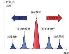
The principles and characteristics of the three main DOFS technologies based on Raman scattering, Brillouin scattering and Rayleigh scattering were compared and summarized, and the research and application status of DOFS systems in the fields of transmission line dancing and lightning strike monitoring at home and abroad were introduced. The shortcomings of overhead transmission line dancing and lightning monitoring technology based on distributed optical fiber sensing were analyzed. It was pointed out that key technologies such as distributed amplification, optical pulse coding, multi-parameter fusion and synesthesia integration would be the next stage of development trend and research hotspot in this field.
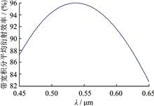
An optimal design method of high polychromatic integral diffraction efficiency(PIDE) was proposed for DOE working within wide incident angle. Through the maximization design of comprehensive PIDE (CPIDE), the design wavelength and the design incident angle were obtained, and the microstructure height could be calculated. The effect of diffraction efficiency on the modulation transfer function of hybrid optical systems was analyzed. A hybrid eyepiece system with DOE was optimized with three lenses. Considering the diffraction efficiency of the DOE, the MTF of the eyepiece system at the maximum field of view was higher than 0.42. This method could provide the basis for image quality evaluation of hybrid optical systems.
As the active layer of TFT, the quality of the IGZO film is very important. IGZO deposition process was investigated and studied to improve the uniformity and stability of the Vth in IGZO TFT process. Firstly, the position of the glass was adjusted to ensure that it was in the middle of the mask. The effect of the angle on the improvement of the uniformity of the thickness of the IGZO film was analyzed to ensure the best magnet swing angle. Finally, the stability of the Vth in the IGZO TFT was ensured by controlling the oxygen pressure in the IGZO process.
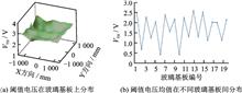
By modifying the lighting fixture of the LCD box and adding a logic operation small box and optical probe, the transmittance of the LCD box was tested. The polarizer was attached to white glass, the polarizer carrier was slotted, and the driving voltage of the LCD box was measured and programmed to match and test the transmittance of the LCD box and module products; Through experiments, it was found that the transmission rate of the optimized and renovated lighting fixture test LCD box was consistent with the fluctuation trend of the module transmission rate, which could meet the needs of LCD box transmission rate screening. Products with high transmission rate fluctuations were intercepted in advance, effectively avoiding the waste of back-end module materials.
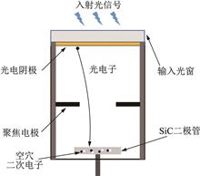
Based on silicon carbide(SiC) wide bandgap semiconductor material and device, the hybrid compatibility of design and fabrication of wide bandgap device and ultra-high vacuum device was realized. A novel hybrid photodetector based on SiC was developed. The effective diameter of the photosensitive surface of the device could reach 25 mm. The electronic bombarded gain was nearly 200 times, and the full width at half maximum(FWHM) of response signal was 4.5 ns. It provided a solid foundation for the theoretical research and engineering application of vacuum and solid‑state hybrid photodetector.
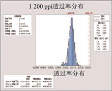
With the continuous development of near-eye display technology, the next generation display technology has more stringent requirements on resolution. In this work, a Langmuir-Blodgett transfer printing (LB-TP) technology was used to realize high-performance quantum-dot light-emitting diodes (QLEDs) with a resolution of 12 700 pixels per inch (ppi). The external quantum efficiency (EQE) of the red QLED device prepared by this method was as high as 15.27%. In addition, a white ultra-high resolution QLED device with an EQE of 4.9% was successfully realized. This work could provide a route for manufacturing of the next generation high resolution display.
A kind of transistor based on graphene heterojunction thin film was introduced, which was fabricated by femtosecond laser technology. According to the principle of preparing graphene by reducing graphene oxide, the graphene was directly prepared on the substrate of Si by femtosecond laser. Finally, the graphene hetero junction thin film transistor (GHTFT) obtained a current on-off ratio of 3.05 × 10². Compared with the graphene transistor before, this value increased by 102. At the same time, the relationship between the current on-off ratio of GHTFT and reduced graphene oxide with different levels was studied. The results showed that with the higher level of reduced graphene oxide, the current on-off ratio of GHTFT was greater, which indicated that femtosecond laser could effectively adjust the electrical properties of GHTFT. In addition, because of the difficulties in preparing graphene at present, the method mentioned in this paper could effectively avoid the transfer process and chemical process. And due to high efficiency, the femtosecond laser could also improve the preparation efficiency of graphene transistors.
An experimental and simulation approach was used to investigate the impact of copper (Cu) content (Cu/In+Ga, CGI) in nanoparticles ink on the performance of copper indium gallium selenide selenium (CIGSSe) solar cells. Firstly, CIGSSe solar cell devices was prepared using different CGI inks and their absorber layers were characterized using scanning electron microscopy (SEM), Hall effect measurements, and Raman spectroscopy. The results showed that as the copper content increased, the crystal growth of the absorber layer gradually improved, and the carrier concentration increased. However, the Cu2-xSe phase became more prominent on the surface. The best experimental conversion efficiency was achieved with CGI of 1.03, and a photovoltaic conversion efficiency of 10.09%. Then a corresponding device simulation model was established to obtain the photoelectric conversion performance, device band structure, and recombination rate distribution of CIGSSe devices with different CGI. The simulation results showed that as the copper content increased and the carrier concentration increased, the open-circuit voltage of the device increased. However, when the carrier concentration exceeded 1018 cm-3, a steep band bending phenomenon appeared on the absorber layer surface, which increased the occurrence of tunneling interface recombination, thereby affecting the device efficiency. Therefore, both the experimental and simulation results suggested that it could be necessary to control the Cu content when preparing CIGS thin-film solar cells to promote crystal growth, reduce interface recombination, and improve device efficiency.
In the study, n-type organic semiconductor material N2200 was doped in p-type organic semiconductor material PDVT-10 to form a trapping center with synaptic characteristics. Metal semiconductor junction formed by contact between organic semiconductor PDVT-10 and silver metal as the source electrode was combined to introduce Schottky barrier, so as to limit the source-drain current of organic synaptic devices, and finally reduce device energy consumption. In addition, the operating current of the devices exhibiting biological synaptic behavior was on the order of 10-10 A, such as excitatory postsynaptic current and other basic synaptic behavior. The scheme has provided a simple and efficient strategy for constructing brain-like neuromorphic computing networks.
A physical layer circuit applied to the data interface of display driver chips was proposed based on Mobile Industry Processor Interface (MIPI) protocol. In response to the increasing speed requirements for data transmission and the issue of offset voltage causing the duty cycle of the output signal to deviate by 50%, which affected the accuracy of high-speed sampling, a multi-stage amplifier structure was adopted to achieve high-speed channels and programmable current source was used for adaptive calibration of offset voltage, reducing the error caused by offset voltage in transmission. The circuit was designed using SMIC 110 nm CMOS technology. The results of post simulation showed that adaptive calibration could reduce the input offset voltage of -30 mV~35 mV to -1 mV~1.2 mV, and the transmission rate of single channel could reach 1.5 Gbps, achieving high-speed and high-precision data transmission.
Purification process of quantum dots could exert great effect on the optical and electrical properties of Cesium lead bromine (CsPbBr3) perovskite quantum dots (PQDs). In this paper, a simple and feasible complex ligand passivation strategy was proposed to modify the surface defects of PQDs. Guanidine bromide (GuaBr) and didecyl dimethyl ammonium bromide (DDeAB) were introduced to modify perovskite quantum dots in the purification process. This ligand passivation strategy could effectively suppress vacancy defects and improve its electrical performance. Finally, based on the quantum dots modified by complex ligands, the green PeLED device could show low performance roll and the maximum brightness of 15 786 cd/m2.
Research progress was summarized on the application of capacitive touch screen in airborne ruggedized display. Compared with the airborne ruggedized display module based on light guide panel, infrared touch screen and resistive touch screen interaction, the airborne ruggedized display module based on capacitive touch screen interaction not only has high touch accuracy and stable performance, but also has a high degree of interaction freedom, which could support real multi-touch and draw, zoom and other operation methods. The paper focuses on the application status of G+G and G+F capacitive touch screens in airborne ruggedized displays, and the application prospects of OGS, On-cell and In-cell capacitive touch screens in airborne ruggedized displays. When the capacitive touch screen formed a large-scale application in the airborne ruggedized display, it would greatly improve the combat performance of military fighters.
The wide-band gap organic material PTB7-Th: PC71BM was used as the front cell, the narrow-band gap organic material PTB7-Th: IEICO-4F was used as the rear cell, and the MoO3/Au/ZnO film was used as the interconnecting layer (ICL) to fabricate a tandem cell. MoO3 / Au / ZnO film was prepared by evaporation and sputtering, which not only had high light transmittance, but also good resistance to solvent erosion. In addition, in order to further reduce the erosion of the solution to the front cell when the cell active layer was spin-coated, chloroform with a low boiling point was selected as the solvent of the rear cell and the dynamic spin coating method was used to reduce the solvent volatilization time. Finally, a tandem organic solar cell with the power conversion efficiency (PCE) of 9.35 % was obtained, which had higher PCE and an open circuit voltage (Voc) of up to 1.4 V compared with single-junction organic solar cells. The results showed that MoO3/Au/ZnO thin films could have great advantages in the preparation of tandem solar cells.
In order to correct distorted images in near-eye display, an image pre-distortion algorithm based on nonlinear fitting and forward mapping interpolation was proposed.The radial basis function fitting algorithm was used to get a more precise mapping relationship between the fitting original image and the pre-distorted image. The compactly supported radial basis function (CSRBF) interpolation algorithm based on forward mapping was used for image gray reconstruction to obtain better correction effect of image distortion. The experimental results showed that the fitting error of the radial basis function fitting algorithm could be reduced to less than 1 pixel, reaching to sub-pixel level. The pre-distortion algorithm had a good correction effect on the distortion produced by the near-eye optical system, which could make the display image clear and complete.