


 View fulltext
Advanced Photonics
Co-Editors-in-Chief
Xiao-Cong (Larry) Yuan, Anatoly Zayats
The authors demonstrate a two-way interaction where the photonic mode affects the liquid film geometry while the latter in turn affects propagation properties of the photonic mode.
Pengfei Xu, and Zhiping Zhou
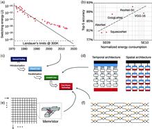
Conventional electronic processors, which are the mainstream and almost invincible hardware for computation, are approaching their limits in both computational power and energy efficiency, especially in large-scale matrix computation. By combining electronic, photonic, and optoelectronic devices and circuits together, silicon-based optoelectronic matrix computation has been demonstrating great capabilities and feasibilities. Matrix computation is one of the few general-purpose computations that have the potential to exceed the computation performance of digital logic circuits in energy efficiency, computational power, and latency. Moreover, electronic processors also suffer from the tremendous energy consumption of the digital transceiver circuits during high-capacity data interconnections. We review the recent progress in photonic matrix computation, including matrix-vector multiplication, convolution, and multiply–accumulate operations in artificial neural networks, quantum information processing, combinatorial optimization, and compressed sensing, with particular attention paid to energy consumption. We also summarize the advantages of silicon-based optoelectronic matrix computation in data interconnections and photonic-electronic integration over conventional optical computing processors. Looking toward the future of silicon-based optoelectronic matrix computations, we believe that silicon-based optoelectronics is a promising and comprehensive platform for disruptively improving general-purpose matrix computation performance in the post-Moore’s law era.
Jul. 06, 2022Vol. 4 Issue 4 044001 (2022)
Zhihao Zhou, Wei Liu, Hengzhe Yan, Xianfeng Chen, and Wenjie Wan
The control of thermal emission is of great importance for emerging applications in energy conversion and thermometric sensing. Usually, thermal emission at ambient temperature is limited to the mid- to far-infrared, according to the linear theory of Planck’s law. We experimentally demonstrate a broadband nonlinear thermal emission in the visible-NIR spectrum within a quadradic nonlinear medium, which emits visible thermal radiation through a pump-driven nonlinear upconversion from its mid-IR components even at room temperature, unlike its linear counterpart which requires ultrahigh temperature. The broadband emission is enabled by the crucial random quasi-phase-matching condition in our nonlinear nanocrystal powders. Moreover, nonlinear thermal emission also permits visible thermometry using traditional optical cameras instead of thermal ones. This scheme paves the way to understand thermal radiation dynamics with nonlinearity in many fields, such as nonlinear heat transfer and nonlinear thermodynamics.
Jul. 06, 2022Vol. 4 Issue 4 045001 (2022)

Dual-modulation difference stimulated emission depletion microscopy to suppress the background signalArticle Video
Wensheng Wang, Chuankang Li, Zhengyi Zhan, Zhimin Zhang, Yubing Han, Cuifang Kuang, and Xu Liu
Stimulated emission depletion (STED) nanoscopy is one of the most well-developed nanoscopy techniques that can provide subdiffraction spatial resolution imaging. Here, we introduce dual-modulation difference STED microscopy (dmdSTED) to suppress the background noise in traditional STED imaging. By applying respective time-domain modulations to the two continuous-wave lasers, signals are distributed discretely in the frequency spectrum and thus are obtained through lock-in demodulation of the corresponding frequencies. The background signals can be selectively eliminated from the effective signal without compromise of temporal resolution. We used nanoparticle, fixed cell, and perovskite coating experiments, as well as theoretical demonstration, to confirm the effectiveness of this method. We highlight dmdSTED as an idea and approach with simple implementation for improving the imaging quality, which substantially enlarges the versatility of STED nanoscopy.
Jul. 06, 2022Vol. 4 Issue 4 046001 (2022)
Quanlong Yang, Dongyang Wang, Sergey Kruk, Mingkai Liu, Ivan Kravchenko, Jiaguang Han, Yuri Kivshar, and Ilya Shadrivov
Control of terahertz waves offers a profound platform for next-generation sensing, imaging, and information communications. However, all conventional terahertz components and systems suffer from bulky design, sensitivity to imperfections, and transmission loss. We propose and experimentally demonstrate on-chip integration and miniaturization of topological devices, which may address many existing drawbacks of the terahertz technology. We design and fabricate topological devices based on valley-Hall photonic structures that can be employed for various integrated components of on-chip terahertz systems. We demonstrate valley-locked asymmetric energy flow and mode conversion with topological waveguide, multiport couplers, wave division, and whispering gallery mode resonators. Our devices are based on topological membrane metasurfaces, which are of great importance for developing on-chip photonics and bring many features into terahertz technology.
Jul. 05, 2022Vol. 4 Issue 4 046002 (2022)
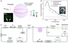
Simultaneous ultraviolet, visible, and near-infrared continuous-wave lasing in a rare-earth-doped microcavityArticle Video
Bo Jiang, Song Zhu, Linhao Ren, Lei Shi, and Xinliang Zhang
Microlaser with multiple lasing bands is critical in various applications, such as full-color display, optical communications, and computing. Here, we propose a simple and efficient method for homogeneously doping rare earth elements into a silica whispering-gallery microcavity. By this method, an Er-Yb co-doped silica microsphere cavity with the highest quality (Q) factor (exceeding 108) among the rare-earth-doped microcavities is fabricated to demonstrate simultaneous and stable lasing covering ultraviolet, visible, and near-infrared bands under room temperature and a continuous-wave pump. The thresholds of all the lasing bands are estimated to be at the submilliwatt level, where both the ultraviolet and violet continuous wave upconversion lasing from rare earth elements has not been separately demonstrated under room temperature until this work. This ultrahigh-Q doped microcavity is an excellent platform for high-performance multiband microlasers, ultrahigh-precision sensors, optical memories, and cavity-enhanced light–matter interaction studies.
Jul. 09, 2022Vol. 4 Issue 4 046003 (2022)
Zhixia Xu, Jie Chang, Jinye Tong, Daniel F. Sievenpiper, and Tie Jun Cui
Controlling energy flow in waveguides has attractive potential in integrated devices from radio frequencies to optical bands. Due to the spin-orbit coupling, the mirror symmetry will be broken, and the handedness of the near-field source will determine the direction of energy transport. Compared with well-established theories about spin-momentum locking, experimental visualization of unidirectional coupling is usually challenging due to the lack of generic chiral sources and the strict environmental requirement. In this work, we design a broadband near-field chiral source in the microwave band and discuss experimental details to visualize spin-momentum locking in three different metamaterial waveguides, including spoof surface plasmon polaritons, line waves, and valley topological insulators. The similarity of these edge waves relies on the abrupt sign change of intrinsic characteristics of two media across the interface. In addition to the development of experimental technology, the advantages and research status of interface waveguides are summarized, and perspectives on future research are presented to explore an avenue for designing controllable spin-sorting devices in the microwave band.
Jul. 19, 2022Vol. 4 Issue 4 046004 (2022)

Chengkuan Gao, Prabhav Gaur, Shimon Rubin, and Yeshaiahu Fainman
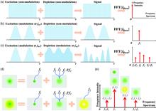
Understanding light–matter interaction lies at the core of our ability to harness physical effects and to translate them into new capabilities realized in modern integrated photonics platforms. Here, we present the design and characterization of optofluidic components in an integrated photonics platform and computationally predict a series of physical effects that rely on thermocapillary-driven interaction between waveguide modes and topography changes of optically thin liquid dielectric film. Our results indicate that this coupling introduces substantial self-induced phase change and transmittance change in a single channel waveguide, transmittance through the Bragg grating waveguide, and nonlocal interaction between adjacent waveguides. We then employ the self-induced effects together with the inherent built-in finite relaxation time of the liquid film, to demonstrate that the light-driven deformation can serve as a reservoir computer capable of performing digital and analog tasks, where the gas–liquid interface operates both as a nonlinear actuator and as an optical memory element.
Jul. 25, 2022Vol. 4 Issue 4 046005 (2022)
Xin Ye, Xiao Qian, Yuxin Chen, Rui Yuan, Xingjian Xiao, Chen Chen, Wei Hu, Chunyu Huang, Shining Zhu, and Tao Li
Microscopy is very important in research and industry, yet traditional optical microscopy suffers from the limited field-of-view (FOV) and depth-of-field (DOF) in high-resolution imaging. We demonstrate a simultaneous large FOV and DOF microscope imaging technology based on a chip-scale metalens device that is implemented by a SiNx metalens array with a co- and cross-polarization multiplexed dual-phase design and dispersive spectrum zoom effect. A 4-mm × 4-mm FOV is obtained with a resolution of 1.74 μm and DOF of 200 μm within a wavelength range of 450 to 510 nm, which definitely exceeds the performance of traditional microscopes with the same resolution. Moreover, it is realized in a miniaturized compact prototype, showing an overall advantage for portable and convenient microscope technology.
Jul. 27, 2022Vol. 4 Issue 4 046006 (2022)
© Copyright 2018-2021 | Chinese Laser Press.
All Rights Reserved 沪ICP备15018463号-20