


Abstract
Quantum vortices of light carrying orbital angular momentum stand as essential resources for quantum photonic technologies. Recent advancements in integrated photonics offer the potential to create and control quantum vortices using fully integrated circuits, eliminating the need for intricate free-space alignment, modulation and the stabilization of bulky optical elements. However, generating quantum vortices in planar optical waveguides and circuits poses challenges, owing to the complexities of confining and guiding twisted photons and, importantly, the difficulties in preparing the quantum superposition and entanglement of vortex states. Here we report the realization of entangled quantum vortex emitters, leveraging programmable integrated nanophotonic circuits. These circuits enable the generation and arbitrary control of resilient vortex entanglement in free space, coherently transitioning from on-chip-created path entanglement. This capability is facilitated by a chip-to-free-space interfacing quantum technology that combines reprogrammable integrated quantum photonics with advanced classical free-space beam structuring. The emitters operate in a plug-and-play manner, enabling swift reconfiguration within microseconds. Validation of multidimensional genuine entanglement is achieved through quantum tomography and measurement of the dimension witness. Our work demonstrates integrated quantum vortex devices that combine the versatility of the on-chip processing quantum information with the robustness of transmitting quantum vortices in free space, opening new avenues for applications in quantum communication, quantum light detection and ranging, and quantum computation and storage.
Main
Quantum vortices embody ubiquitous singular phases in light and matter1,2,3. In particular, optical vortices carrying orbital angular momentum (OAM) in light beams and single photons exhibit distinctive helical-phase structures4,5,6, enabling them to potentially encode a large amount of quantum information. Extensive efforts have been made to explore the quantum entanglement of optical vortices, leading to many important achievements, for example, in strong violation of nonlocality7,8, large-quanta entanglement9,10, multiphoton multidimension entanglement11,12, multimode quantum storage13,14, high-capability quantum key distribution15,16 and teleportation17,18.
The ongoing advancement of quantum technologies with optical vortices demands fully integrated, robust and rapidly reconfigurable OAM devices5,6. Integrated photonics offers a promising avenue for generating and manipulating optical vortices as demanded. However, planar optical waveguides and circuits face challenges in confining and guiding OAM modes due to the difficulty in maintaining helical phases in non-circularly symmetric waveguides19,20,21. This limitation thus hinders the direct generation of the quantum entanglement of OAM modes in waveguides, particularly when intricate nonlinear-optical processes for OAM are imposed. Alternatively, the emerging technology of chip-to-free-space interfacing combines the versatility of photonic circuits in waveguides with the robustness of beam shaping in free space, presenting a promising solution. With this technology, integrated devices can precisely control phases and amplitudes, enabling the free-space formation of helical beams by emitting multiple tailored beams out of waveguides, eventually twisting the wavefront. Pioneering efforts have encompassed both passive and reconfigurable approaches for tailoring the emitted beams. For example, a single microring with multiple passive grating emitters has been realized for classical OAM emitters22,23, OAM lasers24,25 and OAM combs26,27,28. Programmable integrated photonic devices29,30 with multiple individually reconfigurable phase emitters have been explored to shape beams or vortices in free space, for classical telecommunication and light detection and ranging31,32,33,34 and for quantum communication35,36. Moreover, on a single quantum chip, capabilities have been demonstrated for generating and manipulating multidimensional multiphoton entanglement37,38,39 and the processing of quantum information40,41,42, whereas going beyond a single quantum chip out to free space, entanglement distribution and the teleportation of polarized43,44 and spatial modes35 have been reported. Despite the remarkable progress made in reconfigurable light control in waveguide circuits and free-space light-beam shaping, generating the entanglement of vortex states in integrated optical devices remains experimentally challenging. Table 1 summarizes the silicon-based integrated entangled photon-pair sources that have been demonstrated across various degrees of freedom, excluding the OAM entanglement source.
Table 1 Comparison of silicon-based integrated photonic entangled photon-pair sources using various degrees of freedom

Here we demonstrate entangled quantum vortex emitters with programmable integrated photonic circuits. This achievement is realized through the demonstration of a fully integrated optical chip-to-free-space quantum interface, coherently converting robust on-chip path entanglement into OAM entanglement that can reliably transmit in free space. The integrated device performs a Fourier transform on the waveguide modes at different positions to generate a transverse phase gradient and then maps the linear phase to a helical phase, emitting the entangled vortices into free space. The device integrates all components for the generation of plug-and-play vortex entanglement, and it enables the arbitrary and rapid operation of five-mode OAM entanglement by manipulating path entanglement using universal multimode interferometers. The integrated entangled vortex devices can be scaled up to generate more vortices in larger dimensions. The conceptual advancement of chip-to-free-space quantum interfacing not only enables the generation of vortex entanglement with integrated optics but also opens new avenues for practical quantum communication, quantum light detection and ranging, multimode quantum storage and light-atom-based quantum computing applications.
We propose a scheme of generating entangled quantum vortices. It first creates a multi-qudit path-entangled state39 where every qudit is prepared across a number of m waveguiding paths or modes, and it then converts the state to a multi-qudit OAM entangled state where every qudit has a topological charge of l. A coherent conversion of path entanglement and OAM entanglement is shown in equation (1):

where is the logical basis of path-encoded qudits, is the logical basis of OAM-encoded qudits, n represents the number of qudits and d is the local size of every qudit (d is chosen as an odd integer). This scheme enables the generation of an array of entangled vortices with a number of n vortices and a local size of d. Importantly, path entanglement could be arbitrarily operated by universal linear-optic circuits, so that arbitrary OAM entanglement can be generated with integrated optics, beyond any other possible approaches.
Figure 1 shows an integrated-optic device for generating and manipulating the entanglement of two vortices with a local size of five, as an example. Five-dimensional path-entangled qudits are generated by coherently exciting spontaneous four-wave-mixing (SFWM) sources that produce two degenerate single photons (Supplementary Fig. 1)37. The path qudits can be individually manipulated using five-mode universal linear-optic circuits45, yielding arbitrary operations of path entanglement. One key device is the integrated path-to-OAM converter that works as the chip-to-free-space interface, which can be considered as a fully integrated version of the inverse mode sorter using discrete bulk optics46,47 that has been used widely for efficient OAM detection48 and the generation of OAM entanglement49. Our integrated path-to-OAM converter includes three stages: (1) Fourier transform in an on-chip Rowland circle50, which transforms the path mode at the mth input waveguide (a total number of d inputs) to the superimposed mode with a transverse phase gradient of 2πmj/N at the jth output waveguides (j ∈ [0, 1, …, N − 1], where N = 16 is the number of outputs), as shown in Fig. 1b. (2) Phase compensation, which compensates phase distortions from fabrication using an array of individually tunable phase shifters (Fig. 1a). (3) Mapping from the transverse (linear) phase gradient to the angular (helical) phase gradient, by uniformly positioning the N beams around a diffractive circular grating (Fig. 1c)51. The emitted photon possesses a helical wavefront e−il? (? is the azimuthal angle in the cylindrical coordinate system) in the far field, which essentially generates the vortex carrying -order OAM where l = m. That is, the path mode is converted exactly to the OAM mode . We used the inverse of the OAM sorter51 developed in classical optics as the path-to-OAM converter, and operated it in a fully quantum-coherent region so as to flexibly prepare the superposition and entanglement of OAM states with integrated optics. By programming the path entanglement, the device shown in Fig. 1 enables the generation of arbitrary two-vortex five-dimensional entanglement. Details regarding the device design and fabrication are provided in the Methods.\
Fig. 1: Generating quantum vortex entanglement with programmable integrated nanophotonics.
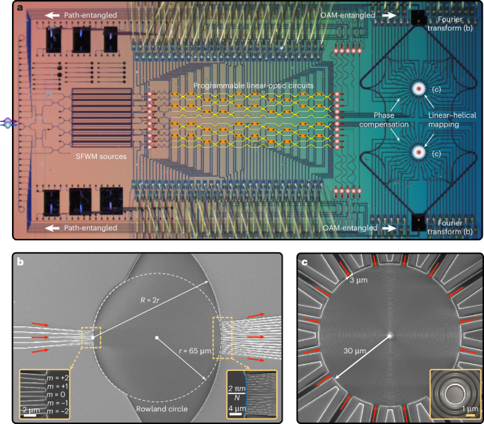
a, Optical microscope image of the entangled vortex chip. The chip, based on silicon nanophotonics, monolithically integrates an array of SFWM photon-pair sources, two sets of universal linear-optic circuits and two path-to-OAM converters. Pairs of degenerate single photons (shown as red-coloured sphere-and-arrow combinations), generated in the integrated SFWM sources from external dichromatic excitations (coloured blue and purple), are subsequently routed by a mesh of crossers, resulting in the preparation of a path-encoding five-dimensional Bell state. The linear-optic circuits with squarely nested Mach–Zehnder interferometers are fully reprogrammable, enabling the arbitrary manipulation of the five-dimensional path entanglement. The two path-to-OAM converters, each of which involves Fourier transform in a Rowland circle (of inner circle radius r and outer circle radius R), phase compensation by an array of optical phase shifters and linear-to-helical phase mapping via a circular grating, emit the entangled vortices to free space for the detection of entanglement. The chip is wire-bound (gold wires) for reconfigurable operations. b,c, Scanning electron microscope images of the on-chip Rowland circle (b) and circular grating (c) structures. In b, the Rowland circle is embedded in a free-propagation region with five input and 16 output waveguides (see the expanded images in the left and right insets, respectively), performing the Fourier transform on the path mode in the mth input to the superimposed mode (indicated by the blue dashed line) with the transverse phase gradient of 2πmj/N at the jth output. In c, the circular gratings implement linear-to-helical mapping, forming a helical wavefront e−il? in free space. They are formed by concentrically etched gratings with a period of 575 nm and a 49% duty cycle (see the expansion in the inset), designed to facilitate the vertical emission of beams and optimize emission efficiency. To reduce losses, tapering structures are used to connect single-mode waveguides with the Rowland circle and circular grating.
We first characterized the integrated-optic path-to-OAM converter. Digital off-axis holography52,53 was used to read out the phase distributions of the emitted OAM light from the circle gratings (Supplementary Fig. 5a). Figure 2a–d shows the holography-measured phase-front distributions for the OAM beams before and after phase compensation. Random phase errors from fabrication were well compensated, by individually optimizing the optical phases in the long waveguides that connect Fourier transform and linear–helical mapping. For the l = {0, 1, 2}-order OAM modes shown in Fig. 2b–d, their uniformly distributed helical phase gradient 2πl/N was confirmed (also shown by the linear fitting in Supplementary Fig. 5b). Moreover, we characterized the modal cross-talk of the emitted OAM beams by performing projective measurements at different OAM bases (that is, the computational Z basis and the superposition F basis) using a spatial light modulator (see Supplementary Fig. 5c). An adaptive moment estimation optimizer was used to optimize the phases to further reduce modal cross-talk, including those from path-state preparation, path-to-OAM conversion and OAM detection. Figure 2e–h shows the measured path-input OAM-output matrices for two vortices. The results show that the matrices have a classical statistic fidelity of 0.97(2). Note that the setting of the phase compensators is to be fixed after calibration, with no need for further operation during the entanglement generation, manipulation and measurement. Furthermore, the near-field images reported in Fig. 2a–d show the presence of higher-order modes. This stems from the spatial discretization of the 16 waveguides transmitting light fields from the Fourier transform unit to the circular grating, leading to the generation of higher-order OAM harmonic modes. In our experiment, we effectively filtered out high-order modes in the far field to ensure high-fidelity OAM entanglement, albeit at the expense of introducing additional losses. This OAM harmonics effect can be mitigated through optimization of the angularly distributed spot size and the number of sampling spots. Detailed analysis and discussion are provided in Supplementary Note 5.
Fig. 2: Characterization of the integrated optical path-to-OAM interface.
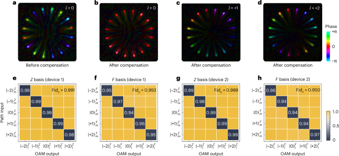
a–d, Digital off-axis holography images of the reconstructed near-field phase distributions of the circular grating before (a) and after (b–d) phase compensation. Bright spots represent the emitted beams carrying a phase gradient of 2πmj/N. In c and d, the gradient phases form the twisted phase front e−il? in the far field. Colours represent the phases and brightnesses represent the light intensities. e–h, Experimental path-input OAM-output matrices for two vortices (devices 1 (e,f) and 2 (g,h)). The matrices are characterized in the computational Z basis (e,g) and the superposition F basis π (f,h), where k = {0, ±1, ±2} and subscripts m and l represent the logical basis of the path and OAM states, respectively. The colours in each matrix grid represent the measured cross-talk ratios. The cross-talk can be characterized via the classical statistic fidelity, , where pi and qi are the experimental and theoretical distributions, respectively.
To confirm the successful generation and manipulation of superposition vortex states and entangled vortex states, we implemented both classical and quantum characterizations, which rely on the detection of bright photon flux and single photons, respectively. For classical characterization, we used high-photon-flux laser light to capture the spatial mode distribution of OAM and OAM superposition states as well as interferometric patterns, which were recorded using an infrared CCD (charge-coupled device) camera—the results are reported in Fig. 3 and the interferometric measurement set-up is shown in Supplementary Fig. 6a. For quantum characterization, we performed full quantum state tomography and entanglement witness measurements to validate the entangled vortex states. This involved detecting single-photon statistics and correlations using superconducting single-photon detectors—the results are shown in Fig. 4 and the experimental set-up is illustrated in Supplementary Fig. 3. When pumped using pulsed light with an average power of 20 mW, we estimated that the device emits OAM–OAM entangled photon pairs at a rate of approximately 200 Hz, primarily influenced by the path-to-OAM converters with a 10.54 dB loss. Detailed characterization of the losses in various components of the circuit, in the free-space OAM projective measurement system and the estimation of the rate are provided in Supplementary Note 4.
Fig. 3: Interferometric measurement and reprogramming of OAM modes.
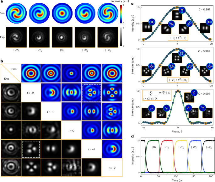
a, Interference patterns between an OAM eigenmode and a Gaussian beam. The OAM states are identified by the number and chirality of the spiral arms. Sim, simulated; Exp, experimental. b, Experimental and simulated far-field intensity patterns of the generated OAM eigenmodes and OAM equal superposition modes. For example, the patterns in the white dashed boxes represent a superposition state of . c, Coherent rotation of OAM superposition states, by swapping the internal phase θ between the two OAM modes and all five OAM modes. Points denote the experimental data (collected with a fixed projection in the spatial light modulator), and the green curves are fitting lines. The insets shows the captured and simulated patterns at different θ values. The contrast (C) is defined as (Nmax − Nmin)/(Nmax + Nmin), where Nmax and Nmin denote the maximal and minimal power, respectively. d, Dynamic reconfiguring of the OAM states by operating the linear-optic circuits. They were driven using a sequence of square waves with a repetition rate of 5 kHz, a duty cycle of 20% and a delay of 40 μs between each one. The rise time, that is, the time interval that it takes the signal to go from 10 to 90% of its final intensity, is measured to be around 7.0 μs.
Fig. 4: Measurement and verification of multidimensional entanglement.
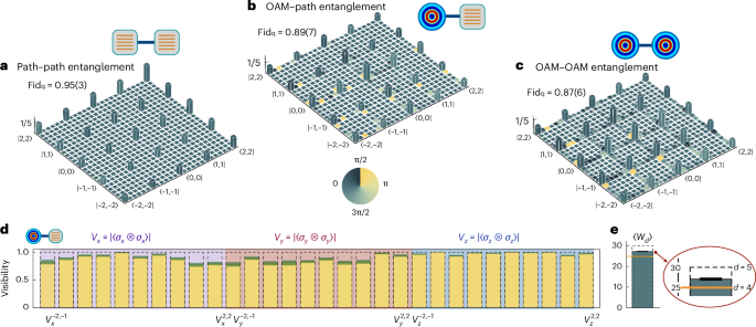
a–c, Experimentally reconstructed density matrices for the path–path entangled state ρpath–path (a), the OAM–path entangled state ρOAM–path (b) and the OAM–OAM entangled state ρOAM–OAM (c). Quantum state tomographic measurements using the compress sensing techniques were implemented to reconstruct the density matrices. The ρOAM–OAM in c was obtained by applying the measured transfer matrix M2 to the measured ρOAM–path in b. Column heights represent the absolute ∣ρ∣ values, whereas the colours represent the ∣Arg(ρ)∣ phases. Phases for matrix elements with ∣ρij∣ ≤ 0.01 are not shown for clarity. The quantum state fidelity Fidq is defined as , where ρ0 and ρ are the ideal and measured states, respectively. The values in parentheses indicate ±1σ uncertainty, estimated from Poissonian photon statistics. d,e, The visibility V (d) and dimension witness W (e) results measured for the five-dimensional entanglement witness of the OAM–path entangled state. In d, the visibilities , where i ∈ {x, y, z} and {a,b} ∈ [−2, −1, 0, 1, 2], are measured in the Pauli bases {σx, σy, σz}, which are indicated by the purple, pink and blue backgrounds, respectively. The yellow-shaded bars denote the experimental results, the teal-shaded areas represent the error bars and the dashed boxes indicate the theoretical values. In e, the measured W value (indicated by the top of the teal column) is estimated to be 27.(2), which exceeds the upper bound of 25 for four-dimensional entanglement (as indicated by the orange line); the dashed box also indicates the theoretical value. The error bars indicate ±1σ uncertainty, estimated from Poissonian photon statistics.
Interferometric measurements were performed to classically characterize the generated OAM beams, by co-axis interfering with a Gaussian reference beam. The interference patterns for the OAM eigenmodes are shown in Fig. 3a, from which the OAM changes l can be read directly from the number and chirality of the spiral arms. The experimental results are in good agreement with the simulations, indicating the generation of high-quality OAM beams via selective path-to-OAM conversion. These generated beams in fact are vector vortex beams, where their polarization state is azimuthally polarized (see Supplementary Note 1 and Supplementary Fig. 4). The measurement of OAM modes is decomposed to those with left-hand and right-hand polarization. During experiments, we detected the left-hand component of OAM states and entangled states. For the ease of reading, in this work, we define l by the interference patterns. Higher-order OAM beams can be generated by shifting the on-chip phases (see Supplementary Fig. 6b).
To generate arbitrary OAM superposition states by controlling the integrated multimode unitary operators, we measured all two-mode superposition states in Fig. 3b. The measured and simulated mode profiles are in good agreement. A continuous rotation of the OAM superposition state was measured via on-chip sweeping of the internal phase θ while keeping the projection basis. High-contrast quantum coherence is observed in Fig. 3c. We also characterized the full-five-mode OAM superposition state of π. At the valleys of the interference fringe, it returns the Fourier superposition modes, whose orthogonality is imaged by the interference patterns. Moreover, to demonstrate dynamic control of the OAM states, a sequence of square waves was applied to the on-chip linear-optic circuits to rapidly reconfigure the generation of vortices switching between different modes. The experimental results in Fig. 3d show sequential excitation of the five OAM states, with a rise time of about 7.0 μs.
We then characterized and certificated multidimensional entanglement. We reconstructed the initial path–path entangled state ρpath–path before conversion (see Fig. 4a) and the OAM–path entangled state ρOAM–path (see Fig. 4b) by performing quantum state tomographic measurements. The OAM–path entanglement can be used for chip-to-chip multidimensional entanglement distributions, keeping one path-qudit on the chip while transmitting another OAM-qudit through free space, and vice versa35. When reconstructing the OAM–OAM entanglement, the two entangled vortices that separately emit OAM photons need to be simultaneously collected and locally measured. In our experiment set-up, the field of view for a long-working-distance objective lens is limited, such that the two vortices cannot be efficiently collected at the same time (the simultaneous detection of two vortex beams is achievable by optimizing the chip design and the measurement set-up—see Methods). We here instead reconstructed the density matrix for the OAM–OAM entangled state by leveraging the transfer matrices for path-to-OAM conversions. The measured transfer matrices (M1 and M2) for the two channels of path-to-OAM conversion are provided in Supplementary Fig. 11. From this, the OAM–path entangled state ρOAM–path can be inferred from ρpath–path and M1 in Supplementary Fig. 12, which is consistent with the tomography result in Fig. 4b. Their compatibility confirms the validness of verifying OAM entanglement. Thus, by applying M2 to the measured state ρOAM–path, it enables the reconstruction of the density matrix for the entangled vortices. The ρOAM–OAM result for the OAM–OAM entangled state is shown in Fig. 4c, and the quantum state fidelity of this is estimated to be 0.87(6). The degradation in state fidelity from path entanglement to OAM entanglement can be attributed to various factors, including inaccuracies and losses in the projection measurements and the experimental set-up (see Supplementary Note 6).
We characterized the entanglement dimension witness for multidimensional entangled states. The dimension witness observable (W) is defined as the sum of interference visibilities in all two-dimensional subspaces10:

where a and b represent the two subspaces, are the interference visibilities measured in the Pauli bases and Na,b is a normalization factor. Figure 4d shows the measured interference visibilities for all combinations of the Pauli measurements, taking the OAM–path entangled state as an example. In Fig. 4e, we estimated the W value to be 27.(2), which exceeds the upper bound of 25 for four-dimensional entanglement, thus successfully verifying the genuine five-dimensional entanglement.
In this work, we have successfully demonstrated entangled vortex emitters using programmable integrated photonics. This device combines the benefits of path entanglement with universal controllability and OAM entanglement with high resilience in free space, enabling the preparation, manipulation and modulation of various quantum vortex states. This demonstration of integrated entangled vortex emitters is the result of the collaborative development of integrated quantum photonics40 and classical free-space beam-structuring technologies in silicon photonics31,32,33,34. The integration of these advanced technologies, along with the intricate preparation, manipulation, conversion and measurement of path and OAM quantum states, establishes the foundation for our work.
In the future, the capability of the device to emit vortices with a higher dimensionality per photon could be enhanced via optimization of the linear-optic circuits37,45 and path-to-OAM converters. The number of entangled vortices can be increased by incorporating multiphoton multidimensional path-entanglement techniques39. The reverse functionality of the OAM emitter can serve as an integrated OAM receiver or mode sorter46,48 for entanglement detection, facilitating the connection of a chip-to-chip quantum system via free space15,16 or an OAM fibre54,55. Enhancing the OAM conversion efficiency is crucial for practical applications and hinges on advancements in integrated photonics (see Supplementary Notes 4 and 5). In a broader context, interfacing free space thorough controllable integrated quantum photonic circuits is vital for a range of practical quantum applications. The adoption of chip-to-free-space interfaces offers the potential to process quantum information on a chip and regulate the transmission of quantum information beyond the chip, which could find practical applications in quantum communication and networks35,44. When combined with high-speed modulation and beam steering32,33, this could enable applications such as quantum light detection and ranging, quantum imaging and metrology. Furthermore, by emitting entangled vortices into free space, spatially structured quantum light fields can be generated for quantum state storage13,14 and trapped-ion quantum computing with integrated optics56.
Methods
Device design
The integrated SFWM photon-pair sources are designed using 1.2-cm-long silicon waveguides with a cross-section of 220 × 450 nm (height × width, respectively), where the phase-matching condition for the FWM process is closely met. In each SFWM source, the two generated degenerate single photons are bunched together. We conducted reverse Hong–Ou–Mandel (RHOM) interference to separate the two Fock photons. Supplementary Figure 1a illustrates the structure, which comprises two sources embedded in a Mach–Zehnder interferometer, resulting in an output state as follows: , where the phase ? is a tunable phase between the two sources, and denote the bunching and anti-bunching biphoton states, respectively, and are the photon number states, is the vacuum state and the subscripts t and b refer to the top and bottom modes, respectively. Supplementary Figure 1c shows the measured anti-bunching term of the RHOM fringe. A high contrast C = 0.99(1) of the RHOM fringe was measured, where the contrast C is defined as (Nmax − Nmin)/(Nmax + Nmin), and Nmax and Nmin denote the maximal and minimal photon counts, respectively. By setting the phase to ? = π/2, we enable the creation of a biphoton state in the two output modes of each source.
The path–OAM conversion in Fig. 1 involves the following components: a Fourier transform based on a Rowland circle, phase compensation using an array of phase shifters and linear-to-helical phase mapping via a circular grating. The Rowland circle is designed with a radius of 65 μm (see the scanning electron microscope image in Fig. 1b) and comprises a free-propagation region that connects five input and 16 output waveguides. Within the Rowland circle, the input light imparts a linear phase gradient of 2πmj/16 (where j = 1, 2, …16 denotes the output positions) onto the 16 outputs under a second-order approximation. This linear transverse phase gradient is dictated by the input state , where m = {−2, −1, 0, 1, 2} signifies the input positions. We utilized three-dimensional finite-difference time-domain simulations to optimize the design of the Rowland circle. The simulation results show a distribution of 16 output intensities with a coefficient of variation (CV) of 4.8%, whereas experimental near-field measurements yielded a CV of 11.7% (see Supplementary Fig. 2b). Discrepancies between the simulation and experimental results could stem from fabrication errors and variations in the coupling efficiency across different regions of the circular grating. On the basis of our simulation findings, when the CV is less than 15%, the cross-talk induced by variations in the 16 output intensities can be disregarded (see Supplementary Fig. 2d), indicating that our devices meet this criterion adequately. Supplementary Figure 2c illustrates the simulated phase distributions of the 16 output spots for the l = 1-order OAM state, demonstrating a linear phase distribution that aligns with the OAM order. In addition, the circular gratings were engineered to vertically emit light beams at a wavelength of approximately 1,550 nm. These diffractive gratings were constructed using 70 nm shallow-etched waveguides with a period of 575 nm and a 49% duty cycle, meticulously designed to achieve phase matching through finite-difference time-domain simulations. The measured phase distributions are presented in Fig. 2 and Supplementary Fig. 5b.
Device fabrication
We fabricated the integrated optical vortex entanglement devices using complementary metal–oxide–semiconductor (or CMOS) processes. The device was fabricated on a 200-mm silicon-on-insulator wafer comprising a 3-μm-thick buried oxide layer and a 220-nm-thick top silicon layer. To define the device patterns, we used a 248 nm deep-ultraviolet (DUV) photolithography process. Initially, a thin layer of positive photoresist was spun onto the wafer, and DUV lithography was used to delineate the full etching and shallow etching structures. The deep etching structures, reaching a depth of 220 nm, were responsible for forming the waveguides and free-propagation regions. On the other hand, the shallow etching structures, with a depth of 70 nm, shaped the circular gratings and input/output gratings. These patterns were subsequently transferred to the silicon layer via a double inductively coupled plasma etching process. Subsequently, a 1-μm-thick layer of cladding oxide (SiO2) was deposited via plasma-enhanced chemical vapour deposition (PECVD). This was followed by the deposition of a 10-nm-thick Ti glue layer, a 20-nm-thick TiN barrier layer, an 800-nm-thick AlCu alloy layer and a 20-nm-thick TiN anti-reflective layer. These layers were patterned using DUV lithography and etching to shape the electrodes (transmission lines typically with a width of 10 μm). An additional 50 nm TiN layer was deposited using PECVD and patterned via DUV lithography and etching to create the resistive thermal-optic phase shifters (with a cross-section of 50 nm × 1 μm (height × width, respectively)). Finally, a thin oxide layer was deposited via PECVD to safeguard the device. Pad windows were then opened for wire bonding by eliminating the deposited oxide layer and the TiN layer above the AlCu. An optical microscope image of the entangled vortex chip is shown in Fig. 1a, whereas scanning electron microscope images showing the on-chip Rowland circle and circular grating structures are provided in Fig. 1b,c.
Measurement of optical vortex states in free space
The detection of OAM states and OAM entanglement was conducted using an off-chip system. This measurement set-up involved collecting the emitted beams using a high-numerical-aperture objective lens and performing standard OAM state analysis, which included two spatial light modulators, two apertures and two single-mode fibre couplers. As the state of polarization of the emitted OAM beams is azimuthally polarized, a combination of quarter-wave plates and polarizers was used to select the left- or right-hand polarized component of the OAM states and entangled states. The experimental set-up for the detection and measurement of entangled vortex states is shown in Supplementary Fig. 3.
On our current integrated devices, the two vortex emitters were designed and fabricated with a separation distance of 1.3 mm. To capture and analyse one of the vortex beams, we used one ×20, 2-cm long-working-distance objective lens along with free-space bulk optical components (see Supplementary Fig. 3). The rationale behind choosing this objective lens was to avert any potential collision with the bonded wires on the chip (for accessing electronic controls for quantum state manipulations). Using an objective lens with a long working distance and a large magnification led to the limited field of view. This means that a single lens was inadequate for efficiently capturing both vortex beams simultaneously. Moreover, the limited space between the two vortex emitters posed challenges in positioning two such objective lenses to capture both vortices effectively. In our experiment, the entanglement properties of the generated vortex beams can be characterized by individually detecting the two vortex states (see main text). However, for future practical quantum information applications, for example, quantum communications and networks, the efficient and simultaneous collection of two or more vortex beams is necessary.
We here discuss several potential solutions to address this issue for future implementations. First, advanced optoelectronic packaging that can eliminate the need for bonded wires in a more compact manner can obviate the need for long-working-distance objective lenses. In this case, replacing a single lens with an array of lens, which is already practical, enables the simultaneous detections of two or even multiple vortex beams. Moreover, redesigning the chip layout is an alternative approach. With the current chip layout shown in Fig. 1, the two vortex emitters are positioned on the same side of the chip, leaving insufficient space between them to accommodate two adjacent objective lenses for light collection simultaneously. In future layout designs, separating the two vortex emitters spatially to opposite sides of the chip with a large space in between will enable the utilization of two distinct objective lenses for reception. Furthermore, in our current experiment, vortex beams are emitted vertically from the chip into free space and analysed using bulk-optic systems. This chip-to-free-space interface is also compatible with optical fibres. This means that the emitted OAM beams can be collected using fibres such as ring-core and OAM fibres, as demonstrated in previous studies54,55. Leveraging these fibres can circumvent the limitations associated with using objective lenses, enabling the simultaneous collection of multiple vortex beams. This approach could potentially provide solutions for chip-OAM fibre–chip systems for applications in quantum communications and quantum networking.