


Abstract
Near-infrared organic light-emitting diodes are attractive for a broad range of applications, including night-time surveillance and biomedical diagnostic and imaging systems. However, obtaining high device radiance, which is necessary for many applications, and maintaining high operational stability is challenging due to the rapid efficiency roll-off at a high current density. Here we develop near-infrared organic light-emitting diodes based on an acceptor–donor–acceptor organic semiconductor with greatly suppressed singlet–triplet annihilation rate and triplet lifetime, alleviating singlet quenching by long-lived triplets, thereby enabling an ultrahigh singlet density at high electrical excitation levels. Our devices exhibit J50 values of 59.2 A cm−2, that is, the current density at which the external quantum efficiency decreases to half its peak value of 1.34%. A high external quantum efficiency is also maintained over a six orders of magnitude range of current densities, at values above 5,000 A cm−2. The devices emit with the maximum radiance beyond 2,000 W sr−1 m−2 under a continuous electrical bias and 46,700 W sr−1 m−2 in the pulsed electrical operation. The half-lifetime is 35 h for an initial radiance of 100 W sr−1 m−2. We also achieve a high electrically injected singlet density of more than 1016 cm−3 at 1,000 A cm−2, which can sustain population inversion, indicating potential for organic lasers. These results pave the way for further developments of near-infrared organic light-emitting diodes as well as offer a potential route towards electrically driven organic laser diodes.
Main
Organic semiconductors emissive in the near-infrared (NIR) region (700–1,000 nm) and corresponding organic light-emitting diodes (OLEDs) are attracting increasing interest1,2 in night-time surveillance, wearable electronics/bioelectronics3 and sensing systems4. NIR OLEDs offer tunable optoelectronic properties, and also being lightweight, mechanically flexible and cost-effective to produce5. Biocompatible NIR OLEDs tuneable within infrared windows to realize deeper penetration into biological tissues are particularly useful for non-invasive in vivo biological imaging6. However, NIR OLEDs are still inferior to their perovskite7 and quantum dot counterparts8 due to their low NIR emission efficiency affected by the energy-gap law9 and the further reduction in efficiency at high current densities owing to exciton-density-driven annihilation processes10,11.
So far, high external quantum efficiencies (EQEs) in the range of 1%–16% have been achieved in NIR OLEDs with phosphorescent12,13,14 or thermally activated delayed fluorescence (TADF)15,16 emitters, whereas maximum EQEs for purely fluorescent NIR OLEDs reach 2% (refs. 17,18,19). However, these values are mostly achieved at low radiances (<10 W sr−1 m−2) (Supplementary Table 1) and low current densities (in the range of 0.001–0.3 A cm−2; Supplementary Table 1), restricting their implementation in practical applications. The decrease in efficiency with increasing current density, called efficiency roll-off10, can be evaluated based on the critical current density J50, which is the current density at which the efficiency drops to half its maximum value. Currently, J50 for NIR OLEDs is within the range of 0.01–1 A cm−2, making them unsuitable for applications in which high radiance is required.
For TADF and phosphorescent emitters in which triplet excitons with a long lifetime are utilized to achieve higher quantum efficiencies, triplet–triplet annihilation (TTA)20 due to the accumulation of slow-decaying triplet excitons is the dominant loss. Purely fluorescent emitters suffer from the annihilation of radiative singlet excitons by different quenching species, such as long-lived triplet excitons (singlet–triplet annihilation (STA))21,22 and polarons (singlet–polaron annihilation)10. Although strategies for suppressed roll-off have been proposed23, the maximum J50 is limited to around a few amperes per square centimetre10,23, owing to the remarkable exciton annihilation loss under high excitation densities. Recently, progress has been made with the acceptor–donor–acceptor (A–D–A) molecular structure for NIR and short-wavelength infrared emission24,25 owing to their superior electronic/optical properties26,27,28,29.
Here we use an A–D–A molecule with a high photoluminescence (PL) quantum yield and negligible STA loss as the emitter, to achieve efficient electroluminescence (EL) and reduced efficiency roll-off at high current densities. We achieved stable and bright NIR OLEDs that can operate at extremely high current densities (over kiloamperes per square centimetre) with the EQE maintained over six orders of magnitude. The device shows the maximum radiance exceeding 46,000 W sr−1 m−2 and on the same order of magnitude as recently reported organic laser diodes30. Moreover, the developed NIR emitters allow the scaling up of large-area single-pixel devices (10 cm2 versus 10−4 cm2 for InGaAs/GaAs light-emitting diodes (LEDs)31), making them ideal candidates for many emerging applications.
Results and discussion
Photophysical properties
A molecule with indacenodithiophene as the central donor unit and 2-(1,1-dicyanomethylene) rhodanine as the terminal acceptor unit (named BTA3 (refs. 32,33); Fig. 1a) was adopted here. The emitter shows intense PL in the NIR region with an emission peak at 740 nm (Fig. 1a) and a high PL quantum yield of 30.9%, among the best NIR organic fluorescent materials18,19.
Fig. 1: Organic semiconductor for ultrahigh-brightness NIR emission.
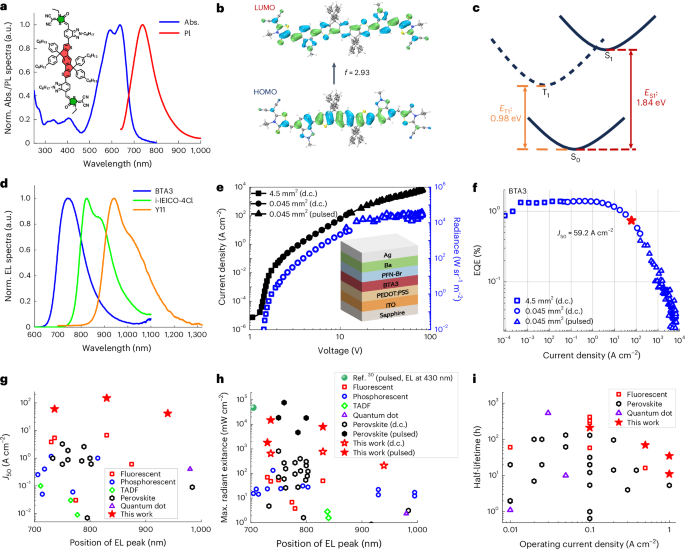
a, Ultraviolet–visible absorption (Abs) and PL spectra of a BTA3 film. The inset shows the chemical structure of BTA3. b, Calculated contour diagrams of the frontier molecular orbitals for BTA3, showing the highest occupied molecular orbital (HOMO), lowest unoccupied molecular orbital (LUMO) and absorption oscillator strength f. c, Energy diagram from the DFT calculations showing the adiabatic singlet excited-state energy (ES1) and triplet excited-state energy (ET1). d, EL spectra of BTA3, i-IEICO-4Cl and Y11 at a current density of 1 A cm−2. e, Current density versus voltage (J–V) and radiance versus voltage (R–V) characteristics of the BTA3 devices. The active area is 4.5 mm2 on a glass substrate (squares) and is 0.045 mm2 on a sapphire substrate (circles) operating in the d.c. driving mode and that of the same device under pulsed conditions (triangles). The inset displays the device structure. f, EQE roll-off characteristics for the BTA3-based NIR OLEDs. Strategies to reduce Joule heating, including the use of a sapphire substrate with a smaller active area of 0.045 mm2 (circles) and driving the devices with pulsed currents (triangles) were successively used, whereas the squares indicate the EQE roll-off characteristics of a routine device with an active area of 4.5 mm2 on the glass substrate. Critical current density J50 (that is, the current density at which the EQE decreases to 50% of its maximum value) of the device is shown with a star symbol. g–i, Critical current density J50 (g), maximum radiant exitance obtained under the d.c. driving mode (open) and pulse driving conditions (solid) (h) and half-lifetime (i) for the best fluorescent, TADF, phosphorescent, perovskite and quantum dot NIR LEDs reported so far. The result of a recently reported indirect electrically pumped organic semiconductor laser with a radiant exitance of 47 W cm−2 and an EL peak of 430 nm obtained under pulse driving conditions is also included for comparison30. All the values in panels g–i can be found in the ‘References’ section and Supplementary Tables 1 and 4.
Frontier molecular levels, adiabatic singlet excited-state energy (ES1) and absorption oscillator strength (f) of the emitter were obtained using density functional theory (DFT) calculation. The calculation confirms a strong overlap between the ground-state and excited-state transition responsible for the NIR emission, leading to a high f of 2.93 (Fig. 1b and Supplementary Fig. 1). There is also substantial overlap between the emission and absorption of the first singlet excited state (S1) (Supplementary Fig. 2), which should be self-quenching of the luminescence. The calculated energy landscape (Fig. 1c) indicates that BTA3 has a low-lying triplet excited state (T1), with a low adiabatic excited-state energy of 0.98 eV. This feature would enable a reduced triplet lifetime, as revealed by later experimental results, because the non-radiative recombination increases with decreasing triplet energy according to the energy-gap law9, thereby minimizing the quenching of radiative singlets by long-lived triplets via STA.
NIR EL
To examine the roll-off behaviour of BTA3 at high current densities, the sapphire wafer substrate (1 mm thick; thermal conductivity, 35 W m−1 K−1), in combination with a patterning strategy for small-area devices (210 µm × 210 µm; Supplementary Fig. 3) was adopted to reduce Joule heating and facilitate heat dissipation34,35. The adopted thermal management techniques were found to be essential to alleviate thermal damage of the devices (Supplementary Fig. 4 and Supplementary Table 2 show the devices using a copper substrate as the heat spreader). A thin layer of Ba cathode was introduced to facilitate electron injection especially at high current densities (Supplementary Fig. 5 and Supplementary Table 3 show the optimization of Ba layer).
The EL spectra of BTA3 devices cover the NIR region (~700–1,000 nm), with a peak wavelength of 740 nm (Fig. 1d). The EL spectra of other typical A–D–A-type molecules with different emission peaks are also included (Fig. 1d), with their device performance discussed below. In the current density–radiance–voltage (J–R–V) characteristics of the device, we note that the BTA3 devices display a low turn-on voltage (Von; voltage at radiance of 1 mW sr−1 m−2) of 1.39 V (Fig. 1e), which is substantially below the bandgap voltage (~1.79 V) of BTA3, in accordance with our previous report24,25. The best-performing device shows a maximum EQE of 1.34% at 5 mA cm−2 (Fig. 1f), which is comparable with some of the highest reported EQEs of 2% (refs. 17,18,19) for purely fluorescent NIR OLEDs (Supplementary Table 1). Moreover, the critical current density J50 is found to be 59.2 A cm−2 (Fig. 1f and Supplementary Table 4), which is more than 10,000 times greater than the current density at which the peak EQE occurs (~5 mA cm−2) and is at least one order of magnitude greater than any fluorescent, TADF, phosphorescent, perovskite and quantum dot LEDs (on the order of 0.01–10 A cm−2; Fig. 1g and Supplementary Table 1). Furthermore, the devices exhibit high efficiency over a wide range of current densities spanning six orders of magnitude (from 10−4 A cm−2 to 102 A cm−2), which is another indicator of extremely small efficiency roll-off. It is also worth noting that although the EQE is nearly doubled to over 2.5% when incorporating 20 wt% of the hole conducting polymer poly[(9,9-dioctylfluorenyl-2,7-diyl)-alt-(4,4′-(N-(4-sec-butylphenyl)diphenylamine))] (TFB) into the emissive layers19. However, J50 decreased noticeably due to the enhanced roll-off triggered by the polymer matrix (Supplementary Fig. 6 and Supplementary Table 5).
Similarly, other A–D–A-type molecules with the EL spectra covering the NIR region between 800 nm and 1,200 nm (Fig. 1d), such as i-IEICO-4Cl and Y11 (Extended Data Fig. 1 shows the chemical structures), exhibit extraordinary performance, with the highest J50 values of 145.9 A cm−2 for the i-IEICO-4Cl device and 41.0 A cm−2 for the Y11 device (Extended Data Fig. 1 and Supplementary Table 4). The ability to operate at high current densities (Fig. 1e), combined with the slow efficiency roll-off characteristics (Fig. 1f and Fig. 1g), not only makes our devices some of the brightest NIR OLEDs reported so far but also enables these OLEDs to rival some of the brightest perovskites and quantum dot NIR LEDs reported so far (Fig. 1h). For instance, the BTA3-based device can sustain a very high current density of 151.1 (132.9 ± 31.6) A cm−2 before thermal breakdown, realizing a maximum radiance of 2,052.9 W sr−1 m−2, corresponding to a maximum radiant exitance of 644 mW cm−2. The i-IEICO-4Cl and Y11 devices yield similar values, reaching high current densities of 200.0 (160.9 ± 52.5) A cm−2 and 277.0 (219.44 ± 50.7) A cm−2 with radiances up to 2,419.2 W sr−1 m−2 and 667.0 W sr−1 m−2 and radiant exitances up to 760 mW cm−2 and 209 mW cm−2, respectively (Supplementary Table 4).
The maximum radiances can be further boosted under pulse electrical operation36, with a pulse width of 1 μs and a duty cycle of 0.1%. In particular, the device can operate at extremely high current densities of 5.0–10 kA cm−2 before thermal damage occurs, reaching a maximum radiance of 46,786 W sr−1 m−2 (Fig. 1f). We note that the EQE at a current density of 1.0 kA cm−2 is 0.13% for the BTA3 device (Fig. 1f) and 0.32% for the i-IEICO-4Cl devices (Extended Data Fig. 1), respectively, which are comparable with those of state-of-the-art perovskite NIR counterparts (for example, 0.6%–1.5%) or that of a recently reported organic laser diode (0.7%)30 (Supplementary Table 6).
Furthermore, the resulting devices achieve operating half-lifetimes of 210 h at 0.1 A cm−2 (with an initial radiance of ~6 W sr−1 m−2) and 35 h at 1 A cm−2 (with an initial radiance of ~100 W sr−1 m−2), whereas the operating half-lifetimes for the glass substrate device obtained under the same current densities are 58 h and 11 h, respectively (Extended Data Fig. 2). To our knowledge, the measured operating lifetimes of our devices represent the best operational stability at a high radiance for high-performance NIR OLEDs and exceed the best results for perovskite and quantum dot NIR LEDs. In particular, the operating half-lifetime at 1 A cm−2 of our devices is approximately seven times higher than that for perovskite NIR LEDs (35 h versus 5 h) (Fig. 1i), thereby representing an important step towards the practical implementation of NIR OLEDs.
Exciton annihilation processes
Time-resolved PL (TRPL) was used first to understand the reduced efficiency roll-off. The PL decay of the neat BTA3 film under light intensities that would trigger singlet–singlet annihilation (SSA) were measured (Fig. 2a). At lower excitation intensities with initial singlet densities below 1015 cm−3, the singlet decay is governed by the exciton lifetime without involving a bimolecular SSA process and follows a monoexponential decay with a rate coefficient (kS) of (1.15 ± 0.05) × 109 s−1. At higher excitation intensities at which the initial singlet densities are much greater than 1015 cm−3, SSA dominates the decay and results in a substantial dissipation of singlet excitons37,38 in the early stages. By fitting the PL decay (Supplementary Note 1), we can extrapolate an average SSA rate coefficient (kSS) of (2.0 ± 1.4) × 10−6 cm3 s−1. The measured value is about five orders of magnitude larger than that of amorphous molecular films10,38 but in accordance with the higher crystallinity and large Förster resonance energy transfer radius of A–D–A molecular aggregated films39,40,41, which prompt exciton diffusion over a long distance. Nevertheless, this strong SSA represents an important quenching source for emissive singlets at high current densities.
Fig. 2: Transient behaviour under optical and electrical excitations and simulated EQE roll-off.
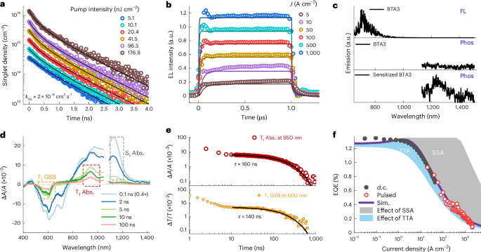
a, TRPL (open circles) of the BTA3 film measured under ambient conditions, where the pump intensity was converted into the singlet excitation density (based on the absorbed photon fluence). Fitting of the curves (solid lines) using Supplementary Equation (2) provides an average kSS value of 2.0 × 10⁻⁶ cm3 s−1. b, Measured transient EL (open circles) of the device. The solid lines display the EL responses simulated based on Supplementary Equations (5)–(7) and the parameters listed in Supplementary Table 7. c, Fluorescence (FL) spectra of BTA3 (pumped at 532 nm) in a toluene solution, and the phosphorescence (Phos) spectra of pristine BTA3 (pumped at 532 nm) and BTA3 triplet sensitized with a lower-bandgap phosphor (BTA3:10 wt% R-CF3, pumped at 380 nm) recorded in toluene solutions with a delay time of 1 ms at 77 K. d, TAS data of sensitized BTA3 (BTA3:5 wt% PtOEP in toluene) pumped at 600 nm with different time delays. The short-lived signal peak at 1,130 nm is ascribed to S1 absorption. The negative and positive peaks at approximately 600 nm and 950 nm that remain after a 10-ns delay correspond to GSB and transient absorption (Abs.) of T1, respectively. The concentration of BTA3 was 10−4 M. e, Triplet decays for the sensitized BTA3 solution probed at 950 nm (triplet absorption, top) and 600 nm (triplet GSB, bottom). The monoexponential decays in the later stages indicate triplet lifetimes (τ) of 160 ns and 140 ns. f, EQE roll-off (purple line) calculated using Supplementary Equations (5)–(7) based on the parameters listed in Supplementary Table 7, along with the measured roll-off of the device (circles). Roll-off without SSA or TTA are shown as grey and blue lines, respectively, with the shaded areas indicating their contributions to the overall roll-off.
Singlet quenching by long-lived triplets (STA) accumulated during high electrical excitation can be revealed by transient EL measurements21,22. When the current injected into the BTA3 device is high, STA starts to dominate singlet quenching as the triplet density increases, and an EL peak followed by a gradual decay to the steady-state intensity (also known as an ‘overshoot’) is usually observed. However, for the device, only minimal signs of overshoot can be observed (Fig. 2b), resulting from the ringing effect of electrical pulse (Extended Data Fig. 3a), indicating negligible STA loss. In general, an negligible STA loss is typically related to a lower triplet density23. To verify this, the triplet energy level of BTA3 was probed at 77 K, to enhance delay phosphorescence from triplets. As shown in Fig. 2c, pristine BTA3 exhibits a prompt fluorescence peak at 710 nm, whereas delayed phosphorescence is negligible owing to the weak intersystem crossing from the S1 to T1 excited states. By contrast, the intensity of the phosphorescence from the T1 emission at 1,240 nm noticeably increases when 10 wt% of the narrow-bandgap triplet emitter R-CF3 (Eg ≈ 1.4 eV; Supplementary Fig. 7) is incorporated as a phosphorescent sensitizer to facilitate cascade energy transfer to the triplet states of BTA3 without accessing the singlet excited states (Eg ≈ 1.8 eV). The deduced low-lying triplet-state energy of 1.0 eV is in perfect agreement with that obtained from our DFT calculations (0.98 eV). Therefore, owing to the low excited-state energy, the triplets in BTA3 are subjected to a high non-radiative decay rate, thereby resulting in a reduced triplet lifetime and a minimal build-up of triplets.
Theoretical modelling of the transient EL decay (Extended Data Fig. 3) gives a high triplet decay rate coefficient (kT) of (7.5 ± 2.5) × 106 s−1 (corresponding to a short triplet lifetime of 0.13 μs; Supplementary Table 7). The fitting of the delayed fluorescence at 5 A cm−2 to the modified rate equations (Supplementary Note 1) yields a TTA rate coefficient (kTT) of (2.0 ± 1.7) × 10−10 cm3 s−1. To provide direct evidence for the reduced triplet lifetime, we performed transient absorption spectroscopy (TAS) using Pt(ii) octaethylporphyrin (PtOEP42; Supplementary Fig. 8a) with a triplet-state energy of 1.91 eV as the triplet sensitizer. Figure 2d shows the TAS spectra for BTA3:5 wt% PtOEP in a toluene solution. The photoinduced absorption peak centred at 1,130 nm shows monoexponential decay with a lifetime of 1.77 ± 0.10 ns (Supplementary Fig. 8b), which arises from the prompt decay of singlet excitons43. The negative and positive peaks at 600 nm and 950 nm are preserved for longer than 10 ns, and can be unambiguously assigned to ground-state bleaching (GSB) and the absorption of triplet exciton, respectively. These long-lived signals exhibited monoexponential decay, with lifetimes of 160 ns and 140 ns (Fig. 2e), respectively, which are even shorter than the triplet lifetime of the triplet sensitizer PtOEP with strong spin–orbit coupling (~200 ns; Supplementary Fig. 8c,d). The results are in line with the value extracted from the delayed fluorescence in the transient EL experiment (130 ns; Extended Data Fig. 3), which further provides strong evidence of a reduced triplet lifetime for BTA3.
To clearly reveal the TTA kinetics in TAS, we sensitized the film blend with 20 wt% PtOEP to populate the triplet states in BTA3 via the short-range triplet–triplet Dexter energy transfer mechanism, bypassing the strong SSA in the BTA3 region (Extended Data Fig. 4). The best fit to the obtained GSB leads to an annihilation rate of 2.0 × 10⁻¹⁰ cm3 s−1, which agrees with the value of kTT determined from the transient EL measurements (Extended Data Fig. 3 and Supplementary Table 7). This large TTA rate presumably results from the higher crystallinity and low energetic disorder in the BTA3 film44, which aligns with the low Urbach energy of 26.9 meV, measured via the sub-bandgap Fourier transform photocurrent spectroscopy (Extended Data Fig. 5).
With the extracted rate constants, we modelled bimolecular quenching processes, including SSA, STA and TTA, on the EQE roll-off using the analytical model described in Supplementary Note 2. The simulated EQE was found to be in excellent agreement with the experimental results (Fig. 2f). We find that TTA and SSA are two significant annihilation mechanisms that have opposite influences on the EQE roll-off, whereas exciton quenching via the STA process is apparently absent because of the reduced triplet exciton lifetime and high TTA rate of the molecule. TTA has a profound effect on alleviating roll-off, especially over a wide current density range between 0.01 A cm−2 and 10 A cm−2, which is consistent with the experimental results shown in Fig. 1f, whereas SSA dominates the drop in the EQE at current densities greater than 10 A cm−2.
Therefore, the significance of a high TTA rate coefficient is twofold. First, it leads to a decrease in the triplet density, thereby decreasing the probability of singlet exciton quenching via STA. Second, TTA can generate additional singlet excitons from triplet excitons, which is particularly important for high-radiance applications that require elevated injection levels. These effects are especially relevant for organic laser diodes, where various losses under high excitation, such as bimolecular annihilation processes, remain major obstacles that prevent electrically driven lasing45,46.
Amplified spontaneous emission
To demonstrate the potential of BTA3 as a gain medium in organic lasers, we investigated the lasing threshold behaviour of BTA3 via amplified spontaneous emission (ASE) experiments (Fig. 3a), in which the intrinsic singlet decay and SSA are the only two loss channels for the optically generated singlet excitons. The excitation density dependence of the PL spectra of the BTA3:4,4′-bis(9H-carbazolyl)-2,2′-biphenyl (CBP) (10 wt%:90 wt%) film as a gain medium at an excitation photon energy of 3.61 eV (343 nm) is shown in Fig. 3b. CBP was incorporated to passivate the lossy, wrinkled surface structure of neat BTA3, enabling improved optical feedback for light amplification (Supplementary Fig. 9). When pumped above the threshold of 1.36 μJ cm−2 (Fig. 3c), dramatic spectral line narrowing from 102 nm down to 46 nm and eventually to 12 nm is observed (Fig. 3b), which is indicative of light amplification. Films with higher BTA3 content show similar ASE thresholds (Supplementary Fig. 10). Benefiting from the high f and high PL quantum yield, BTA3 has one of the lowest threshold for ASE among red/NIR organic materials so far, which is more than four times lower than the best reported values (1.36 μJ cm−2 versus 7–21 μJ cm−2; Fig. 3d and Supplementary Table 8), making it a promising candidate for organic injection lasers.
Fig. 3: ASE measurements of BTA3 and simulated singlet and triplet densities.
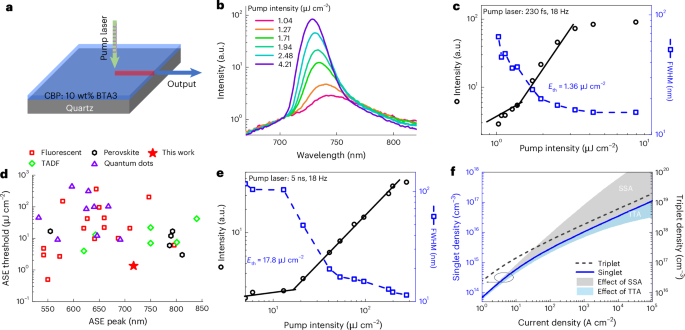
a, ASE measurements for the CBP:BTA3 film on a quartz substrate under 343-nm laser excitation. Singlet excitons of BTA3 are efficiently populated via efficient host–guest Förster resonance energy transfer from the CBP host to BTA3. b,c, PL spectra normalized to the intensity at 675 nm (b), and intensity and full-width at half-maximum (FWHM) of 10 wt% BTA3 doped in CBP films at different excitation fluences of a pulsed laser (duration, 230 fs; wavelength, 343 nm; repetition rate, 18 Hz; beam size, 1.0 mm × 4.3 mm) (c). d, Comparison of the ASE thresholds of various lasing materials with emission beyond 500 nm (Supplementary Table 8). e, ASE thresholds of CBP:10 wt% BTA3 when excited by a 532-nm neodymium-doped yttrium aluminium garnet laser (Q-smart, QSM-100-20-G) with a pulse duration of 5 ns and a repetition rate of 18 Hz. f, Simulated singlet (blue solid line) and triplet (black dashed line) densities as a function of current density for the device; the contributions of SSA and TTA to the overall singlet density are illustrated by the grey and blue areas, respectively.
To validate its potential for light amplification by electrical pumping, ASE measurements using a nanosecond laser were performed to provide better analogy to a nanosecond electrical pulse (Fig. 3e and Extended Data Fig. 6). During nanosecond pumping, SSA (a sub-nanosecond process) is fully activated compared with ultrafast femtosecond excitation, which raises the ASE threshold to an average value of 20 μJ cm−2. The photon flux is equivalent to an electrical pulse of 6.9 kA cm−2, which is the current density required to achieve electrically pumped ASE. Nevertheless, we believe that this electrical pumping threshold can be further reduced by introducing a high-quality resonator39 or suppressing the SSA.
To verify the feasibility of using the BTA3-based device in lasing applications, we calculated the singlet and triplet densities as a function of the current density for the device (Fig. 3f) by taking the contributions of SSA and TTA into account. We infer that a singlet density of 1016 cm−3, which is necessary to reach the lasing threshold47, can be produced by a threshold current density of 1 kA cm−2. However, a threshold current density greater than 5 kA cm−2 is required to exceed the lasing threshold when TTA is absent. By contrast, if SSA can be completely mitigated, the threshold current density would greatly decrease to 100 A cm−2.
NIR imaging, flexible optoelectronics and illumination
The low driving voltage confirmed by a drift–diffusion model (Extended Data Fig. 7 and Supplementary Note 5) suggests great potential for easy implementation as portable NIR light sources. Owing to the limitation of small-area size (~0.01 mm2), present state-of-the-art InGaAs/GaAs multiquantum-well NIR LEDs exhibit a typical maximum optical power of around 10 mW (ref. 31). The use of a spin-coating procedure enables the fabrication of cost-effective and bright NIR light sources with a large area of 10 cm2 in the laboratory for prototyping (Fig. 4a). The devices can have both high radiance (up to 2,000 W sr−1 m−2) and high NIR power, providing access to the biologically transparent window in the range between 650 nm and 1,350 nm. Accordingly, we can demonstrate, as a proof of concept, non-invasive biological imaging applications of our devices. Our devices can achieve not only high-resolution (that is, 100 μm) bioimaging of human finger blood vessels in the transmission mode (Fig. 4b) and of the main organs of live Xenopus laevis (Fig. 4c) but also the dynamic imaging of heart arteries of a tortoise to quantify the heartbeat rate (Supplementary Video 1). To the best of our knowledge, this is the first demonstration of an NIR OLED in vivo biological imaging system with performance comparable with NIR fluorescence imaging systems6, but with the substantial advantages of ease of use, non-toxicity and non-invasive analysis of biological tissues. The devices fabricated on a flexible substrate show good mechanical bending capability (Fig. 4d), rendering them suitable for biomedical applications in which intimate integration with the human body is required. Figure 4e shows the image of a wearable OLED patch attached to a finger, which can be used to wirelessly transmit physiological data from the tissue of interest to optical sensors due to their high tissue penetration depth and high radiance. Despite being in its infancy, we anticipate that when combined with advanced optical microscope systems and flexible substrates, our prototype NIR bioimaging system can provide new functionalities beyond those required by the assessment of atherosclerosis, detection of cancer and intraoperative image-guided surgery.
Fig. 4: Demonstration of large-area NIR light sources based on BTA3 and their applications.
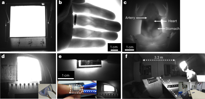
a, Picture of a large-area flood light source with a size of 10 cm2 (3.2 cm × 3.2 cm) driven by a current density of 5 mA cm−2. b, Images of subcutaneous blood vessels of human fingers under the transmitted illumination of large-area NIR OLEDs. c, Image of the major organs in the body of X. laevis. d,e, Flexible and uniform large-area NIR OLEDs (1.5 cm × 1.5 cm) based on BTA3 (d) and the application of the flexible device in wearable devices for optical monitoring (e). f, Night-vision photograph of a conference room under the illumination of flood NIR OLEDs based on BTA3 at 150 mA cm−2. The insets in d–f show the photographs of the same scene under illumination of fluorescent tubes.
We also demonstrate that our devices have promising potential as light sources in night-vision technology (Fig. 4f). At a current density of 0.15 A cm−2 and a bias of 2.8 V, the devices exhibit a high optical power of 30 mW, which provides sufficient radiance for indoor or near-distance security applications. Our single-pixel devices have the potential to provide 1 W or even higher optical power; hence, their list of potential applications will continue to grow, spanning from food and environmental monitoring to on-chip optical communication and emerging portable applications.
Conclusions
Overall, we demonstrate NIR OLEDs with very high radiance and long-term operational stability by using A–D–A-type organic molecules as the emissive layer. The devices retain their high NIR EL efficiency over a wide current density range spanning more than six orders of magnitude and maintain half of their maximum efficiencies at high current densities of tens of amperes per square centimetre, representing one of the smallest efficiency roll-offs among organic light-emitting devices so far. Furthermore, the devices can operate at ultrahigh current densities on the order of 1,000 A cm−2 with noticeable efficiency under pulsed electrical excitation conditions. We find that the distinctive efficiency roll-off characteristics arise from the nature of the exciton-density-driven annihilation processes in the molecule, which result in negligible STA loss for a high singlet density and a high TTA rate that leads to the further generation of additional singlet excitons from triplet excitons. The fast radiative recombination of the emitter leads to a very low threshold for ASE in the NIR region. Our new understanding suggests that SSA is the fundamental limitation to a minimal roll-off towards NIR organic laser diodes. The process should be further mitigated, for example, through reducing accessible higher-excited states via molecular design and, therefore, inhibiting resonant energy transfer or by suppressing dipole–dipole interaction by tuning the molecular packing. We demonstrate the potential of these devices for emerging applications ranging from biomedical imaging modalities to night-time surveillance. Our results represent significant progresses towards stable, high-radiance NIR OLEDs, and our devices have the potential to form the basis of organic laser diodes.
Methods
Materials
A–D–A-type molecules BTA3 (refs. 32,33) and Y11 (ref. 48), interlayer material poly[(9,9-bis(3-(N,N-dimethyl)-N-ethylammonium)-propyl)-2,7-fluorene-alt-2,7-(9,9-dioctylfluorene)]dibromide (PFN-Br; ref. 49), host material F8BT and triplet emitter PtOEP (ref. 47) were obtained from 1-Material. A–D–A-type molecule i-IEICO-4Cl was prepared using a synthesis route described in our previous paper50. Triplet emitter R-CF3 was synthesized according to a previous report51. Electron transport layer PDINO and host material CBP, TFB and OXD-7 were purchased from Sigma-Aldrich. Poly(3,4-ethylenedioxythiophene):poly(styrene sulfonate) (PEDOT:PSS; Clevios P VP AI 4083) in an aqueous solution was purchased from H.C. Starck. All the purchased chemicals were used as received without additional purification.
Computational methods for molecular orbital wavefunctions and energies
The geometries of these two molecules in the ground state were optimized with dispersion-corrected DFT (DFT-D3) at the B3LYP-D3/6-31G(d,p) level using the Gaussian program52. The excited electronic structures of the molecule were calculated at the PBE0-D3/def2-TZVP level using the time-dependent DFT method, and the excited energy and oscillator strength were obtained from the calculation result at the same time. The molecular geometries at the S1 and T1 states were also optimized at the PBE0-D3/def2-SVP level, and more accurate time-dependent DFT calculations were performed at the PBE0-D3/def2-TZVP level. The spin–orbit coupling matrix elements were calculated using the spin–orbit mean-field methods based on the excited-state wavefunctions obtained from the time-dependent DFT calculations. All these calculations were performed using the ORCA v. 5.0.2 program. The visualization of the frontier molecular orbitals was rendered using the Visual Molecular Dynamics program (v.1.9.3).
Device fabrication and characterization
NIR OLEDs are made using the following device architecture: sapphire/indium tin oxide (ITO; 100 nm)/PEDOT:PSS (30 nm)/BTA3 (100 nm)/PFN-Br (5 nm)/Ba (3 nm)/Ag (200 nm). The devices were fabricated on patterned ITO-coated sapphire substrates, provided by Guangzhou New Vision Optoelectronic Technology, whereas the flexible polyethylene terephthalate substrate was provided by Jinghui Optoelectronic Technology. After wet-cleaning and air-plasma treatments, a 30-nm-thick PEDOT:PSS 4083 anode buffer layer was spin cast on the cleaned and dried substrate. Subsequently, the NIR emissive layer was deposited using the spin-coating method from its chloroform solution for i-IEICO-4Cl and Y11 (concentration, 15 mg ml−1) and from a toluene solution for BTA3 (concentration, 20 mg ml−1) to form a uniform 100-nm-thick film on top of the anode buffer layer. For doped devices based on BTA3 and TFB, the total concentration of the host (TFB) and guest (BTA3) is limited to 20 mg ml−1, and the solvent is toluene. Subsequently, the electron transport layer (PFN-Br; 0.6 mg ml−1 in methanol) is also fabricated by the spin-coating method. Finally, a thin layer of 3-nm-thick Ba and 200-nm Ag layer were evaporated with a shadow mask under a pressure of 1 × 10⁻⁴ Pa. The active area of the device is defined by the overlap between the Ba/Ag cathode and ITO anode. Before device characterization, all the devices were encapsulated using a glass coverslip and an ultraviolet-cured epoxy resin in a nitrogen-filled glovebox. For the rollable devices, the same device structure and spin-coating process as for the glass or sapphire substrate were used; the flexible polyethylene terephthalate substrate was provided by Jinghui Optoelectronic Technology.
J–V characteristics of devices under the d.c. driving condition were obtained using a Keithley 238 source meter unit, whereas the R–V characteristics were simultaneously recorded using a calibrated silicon photodiode. The driver of the J–R–V system under the d.c. condition is set up in LabVIEW (v.18.0), and the detector signal is captured at 500-ms intervals after the device is activated during testing. The average signal strength of ten readings taken over the next 1,000 ms is recorded as the output result. For J–R–V characteristics under pulsed excitation, a J–R–V test system (PL202, Wuhan Precise Instrument) was used to record the J–R–V characteristics. For EL spectroscopy and EQE measurements, the radiance and spectra of EL were recorded using a spectrometer (QE Pro, Ocean Optics) by collecting the emitting photons in all directions through an integrated sphere. The EQE was calculated by dividing the number of photons extracted by the number of electrons injected per unit time. The spectrometer was calibrated from 350 nm to 1,100 nm using a standard halogen calibration light source (HL-3 plus-INT-CAL).
TRPL spectroscopy measurement
The steady-state PL and TRPL spectra were measured using a time-correlated single-photon counter (HydraHarp 400, PicoQuant) coupled to a single-photon-counting photomultiplier tube detector with high photoresponse at a wavelength of 720 nm. The samples were periodically excited by a 410-nm femtosecond Ti:sapphire pulsed laser (Coherent) with a pulse duration of 120 fs, a maximum fluence of ~0.2 µJ cm−2 per pulse and a repetition rate of 80 MHz. A set of neutral attenuation sheets with different pass rates were used to adjust the pump light intensity. To minimize the scattering of incident laser light, a long-pass filter with a cut-off wavelength at 520 nm was placed before the detector.
Time-resolved EL measurement
The transient EL measurements were performed using a high-power programmable pulse generator from Keysight (Agilent 8114A, 100 V/2 A) to generate appropriate excitation waveforms. The pulse repetition rate was 1 kHz with a duty cycle of 1%. The EL signal was detected using a lens coupled with an optical fibre connected to a photomultiplier tube (Hamamatsu, H10721-20), and the output signals were then fed into a digital phosphor oscilloscope (Tektronix DPO5204B).
ASE measurement
The films were excited by a third harmonic laser beam of a ytterbium-doped potassium gadolinium tungstate laser (PHAROS, LIGHT CONVERSION) with a centre wavelength of 343 nm, a pulse width of 230 fs and a repetition rate of 18 Hz or pumped by a neodymium-doped yttrium aluminium garnet laser (Q-smart, QSM-100-20-G, Quantel Laser) with a repetition rate of 18 Hz, a laser pulse width of 5 ns and an excitation wavelength of 532 nm. After passing through an aperture and a neutral attenuation sheet, the pump light is directed by a cylindrical lens to create a small stripe (1.0 mm × 4.3 mm). The spectrum of emission was collected by a spectrometer (USB2000+, Ocean Optics) in the waveguide mode. A 100-nm-thick optical gain film was fabricated on a quartz substrate by spin coating. The total concentration of the host–guest-doped film in different proportions was controlled at 20 mg ml−1, and the solvent was chloroform. All of the tests were conducted at room temperature.
TAS measurement
TAS measurements were acquired on a pump–probe ultrafast spectroscopy system (HELIOS EOS Fire, Ultrafast Systems). Excitation was performed with a femtosecond pulsed laser (wavelength, 800 nm; pulse length, 80 fs) generated by a Ti:sapphire laser system (Astrella, Coherent). The pump pulse (600 nm or 380 nm) was generated through an optical parametric amplifier (OPerA Solo, Coherent). The white-light probe beam (350–950 nm and 750–1,600 nm) was generated by an electrically pulse-triggered nanosecond laser. After passing through a depolarizer, the pump beam was focused and overlapped with the probe beam atop the sample. Time-resolved detection of the spectra was achieved by introducing a variable time delay between the pulsed excitation and operation of the detecting gate. The TAS measurement was performed on a sample thickness of 100 nm at a series of pumping intensities between 20 μW cm−2 and 500 μW cm−2 by monitoring the transmitted light through the samples. For solution samples, a diluted solution (1 × 10⁻⁵ M) in toluene was used. All tests are performed in air at room temperature. All solutions and films were carefully sealed and encapsulated in a glovebox to avoid oxygen quenching.
NIR optical imaging and illumination
The light source for NIR optical imaging and illumination is based on devices with an area of 10 cm2, with a device structure similar to that shown in Fig. 1e, but on a patterned glass/ITO substrate or a flexible polyethylene terephthalate substrate. In case of currents lower than 1 A, the devices were driven by a digital source meter (model 2400, Keithley), whereas in the a higher-current region, the devices were driven by a high-power d.c. supply (model UTP3000TFL-II, UNI-T). All the NIR photographs were captured by an NIR camera (model ASI462MM, ZWO) with a long-pass filter, which had a cut-off wavelength of 700 nm.