


Abstract
Highly efficient, ultrahigh-density inorganic micro-LED displays are gaining a strong position in the market for use in augmented reality glasses. When applied to electronic contact lenses with an eye-adaptive form factor, the micro-LED displays evolve into next generation augmented reality viewers. Here, we report 1-nm-thick epitaxial AlN passivation for 1.5-μm-diameter InGaN red micro-LEDs with high external quantum efficiency of 6.5% at the peak wavelength of 649 nm. The flexible form factor of the red micro-LEDs is achieved through the development of a near-complete device transfer. By overcoming the existing bottlenecks of red spectral efficiency and form factor of inorganic micro-LEDs, we believe this will pave the way for another revolution in the augmented reality and metaverse industries.
Introduction
Inorganic micro-LED (μ-LED) displays exhibit both high brightness and a contrast ratio superior to those of OLED and reflective LCD displays. They are particularly suited for the application of augmented reality (AR) glasses, as they have high potential for realizing high pixel densities1,2,3. AR glasses require both seamless, realistic human vision and a slim form factor. The slim form factor can be achieved with ultrahigh density (UHD) μ-displays coupled with waveguide-type image delivery, suffering from inherent low light-transmission efficiencies (<0.5%). For this, μ-LED displays with small light-emitter size (<2 μm), ultrahigh brightness (>105 nit) and external quantum efficiencies (EQEs) of >5% are essential. It was recently reported that a mesa-etching approach provided blue InGaN nanorods with diameters of 0.6 μm that exhibited an EQE of 21 and 22% by surface passivation with sol-gel or atomic layer deposition (ALD) of HfO2–based layer4,5. However, one of the critical challenges to realizing UHD RGB displays is the low EQEs of inorganic μ-LEDs in the red spectral range. AlGaInP red μ-LEDs suffers low EQE of ~0.1% at the emitter size of <5 μm, which is attributed to high non-radiative surface recombination6. At large size (1 mm × 1 mm) flip-chip geometry, recently reported InGaN LEDs has quite high bulk EQE of 10.5% at 625 nm7. Down to a diameter of 25 μm InGaN μ-LEDs, the peak EQE of ~5% at ~630 nm is achieved using Al2O3 surface passivation8. Reference 8 also shows that the red EQE decreases significantly with decreasing emitter size from 100 to 25 μm, suggesting much lower EQE estimated for the size less than at <5 μm. For the commercialisation of μ-LED UHD displays, a breakthrough in surface passivation technology is essential to ensure high EQE for red μ-LEDs with diameters less than 2 μm, which is not yet achieved.
Flexible form factor is another bottleneck of inorganic UHD μ-LEDs to conform various AR device forms. Electronic contact lens can be a good example, offering a seamless and comfortable user experience encapsulated within an incredibly sleek and slim form. For realizing flexible UHD inorganic μ-LEDs, one could explore the transfer of individual μ-LED chips onto a flexible TFT backplane or copper-to-copper hybrid bonding between μ-LEDs and CMOS backplanes9,10,11. However, such processes can hardly be used due to the fundamental limit of flexible substrates for high-precision alignment or high-temperature processing. Therefore, monolithic integration of μ-LEDs/driving circuit and its transfer onto flexible substrates are inevitable for flexible inorganic UHD μ-displays.
Here, we report 1-nm-thick epitaxial AlN passivation for 1.5-μm-diameter InGaN μ-LEDs with EQE of 6.5% at the peak wavelength of 649 nm by local heating-based ALD. Furthermore, the flexible form factor is achieved through the development of a near-complete device transfer of the red μ-LEDs on a polyimide (PI) substrate. By breaking the red spectral efficiency and form factor bottlenecks, we believe our study can provide a paradigm for highly efficient, flexible UHD RGB displays that can expand the range of AR applications, including electronic contact lenses.
Results and discussion
Epitaxial aluminium nitride passivation
Figure 1 illustrates the epitaxial passivation of ultrathin single-crystalline AlN (e-AlN) passivation for high efficiency in the red spectral region. The e-AlN is formed on the circumference of nano-LED or μ-LED emitter surfaces by devising an Ar plasma-assisted ALD process (Fig. 1a, b). With lattice parameters of AlN (a = 3.11 Å, c = 4.98 Å) and GaN (a = 3.19 Å, c = 5.19 Å), their epitaxial atomic arrangement between AlN and (In)GaN is sketched (Fig. 1c). To obtain a highly efficient light emitter even at the submicrometer scale, it is essential to minimize nonradiative recombination at the surface of multiple-quantum wells (MQWs). This is often achieved with optimized chemical or field-effect passivation. The former is achieved by chemically eliminating dangling bonds at the semiconductor surface with a dielectric film. The degree of nonradiative recombination is associated with the interface trap density (Dit). The latter is achieved by establishing a surface electric field that repels one type of carrier and therefore limits the recombination capacity at the interface (field effect). It can be determined from the fixed charge density (Qf). HfO2 is often used as a passivation layer due to its low Qf value12. A positive or slightly negative Qf is required to reduce the hole (minority carrier) concentration at the surface in undoped or n-GaN. This minimizes nonradiative recombination and achieves high efficiency. In this work, we developed a more advanced method called AlN-based epitaxial passivation (e-AlN) to achieve both ideal chemical (low Qit) and field-effect passivation (low Qf)13. Here, the (In)GaN surface to be passivated is non-polar m-plane, in which both spontaneous and piezoelectric polarization charges (Qp) are absent14. Despite the absence of Qf and/or Qp, there is still an equilibrium energy band bending, hence electron accumulation or increase at the AlN/GaN heterointerface via equalization of the Fermi level, as sketched in Fig. 1d. We note, however, that this does not affect the field effect passivation of e-AlN or increase non-radiative recombination, as the electron is a majority carrier in (In)GaN MQWs.
Fig. 1: The epitaxial AlN (e-AlN) passivation for highly efficient red InGaN/GaN μLEDs.
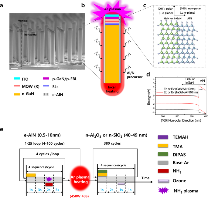
a SEM image of the red InGaN nanorod array coated with an epitaxial passivation layer. b The schematic of e-AlN formation by Ar plasma-assisted ALD. MQW (R), SLs, and p-EBL represent red InGaN/GaN multiple quantum wells, InGaN/GaN superlattices, and p-type AlGaN electron blocking layer, respectively. c Atomic arrangement at the passivated interface between e-AlN and non-polar GaN or InGaN. d Corresponding equilibrium bandgap diagram of (c). e Timing sequence of the Ar plasma-assisted ALD for e-AlN (0.5–10 nm) + n-Al2O3 or n-SiO2 (40–49 nm). TEMAH, TMA, and DIPAS represent tetrakis(ethylmethylamino) hafnium (hafnium precursor), trimethylaluminium (aluminum precursor), and di-isopropylamino silane (silicon precursor), respectively. A scale bar, 2 µm (a).
The e-AlN is fabricated by the Ar plasma-assisted ALD (Fig. 1e). Although ALD is often used as a passivation method for complex 3D structures due to its superior conformality, ALD AlN layers are typically amorphous or polycrystalline. Here, we realise the epitaxial growth of ultrathin single crystalline AlN on the sidewalls of nano- and μ-LEDs. Our approach features introduction of the Ar plasma ignited between ALD growth cycles15,16, as compared to that of conventional ALD (Supplementary Fig. 1a). The in-between Ar plasma generates local heating that provides thermal energy to arriving precursors for the atomic rearrangements on (In)GaN LED sidewall surfaces to form epitaxial AlN (Fig. 1b). In detail, the process is designed to ignite the Ar plasma after every 4-ALD-cycles (Fig. 1e and Supplementary Fig. 1b) to minimize the surface roughness of the passivation layer while maintaining an epitaxial relationship. The details of ALD timing sequences are described in “Methods”. It should be mentioned that the nano- and μ-LED m-plane sidewalls vertical to the substrate surface are much more beneficial for epitaxial passivation compared to horizontal c-face epilayers. This is because there was little Ar plasma-induced physical damage on the vertical sidewalls with nearly parallel to the direction of ion bombardment.
To prove the concept of epitaxial passivation, we first grew e-AlN on c-plane p-type GaN using the suggested method. Both high-resolution transmission electron microscopy(HR-TEM) and atomic high-angle annular dark-field scanning TEM (HAADF-STEM) images clearly reveals hetero-epitaxy between c-plane GaN and AlN (Fig. 2a–f). However, inspection of the figures shows that with increasing thickness in the range of 0.8–5.6 nm, the e-AlN exhibits uneven contrast (Fig. 2a–c) or poor lattice ordering (Fig. 2d–f). This suggests that the crystalline quality of the thicker e-AlN may be lower due to lattice mismatch. Next, we coated a InGaN-based nanorod LED array with various passivation layers to form core/shell structure (Supplementary Fig. 2). The n-HfO2/AlN/Al2O3/SiO2 represents normal or conventional amorphous HfOx/AlN/Al2O3/SiO2 ALD without Ar plasma heating (Supplementary Fig. 1a). The vertical and horizontal cross-section of the e-AlN coated nanorod (Fig. 1a) is characterized by HR-TEM (Fig. 2g–m). Inspection of Fig. 2g–i with coating of e-AlN (10 nm)/n-AlN (40 nm) reveals there exist hetero-epitaxy between AlN and (In)GaN m-plane sidewalls. We note that the e-AlN layer appeared to extend to more than 10 nm, probably because of the nature of the n-AlN that was easily crystallized. When combined with other amorphous layers, such as SiO2 and Al2O3, e.g., AlN/SiO2 and AlN/Al2O3, 10-nm e-AlN was clearly visible (Fig. 2j–m). However, Fig. 2g–i again shows uneven contrast, suggesting existence of defects for the 10-nm-thick e-AlN passivation layer due to lattice mismatch between (In)GaN and AlN. Importantly, for ultrathin (~2-nm-thick) e-AlN, we can observe conformal and clean AlN/(In)GaN hetero-epitaxial relationship on m-plane sidewalls (Fig. 2j–m). We claim that the suggested ALD process enables such ultrathin e-AlN on the sidewall, importance of which is ability to make the thickness close the critical thickness (tcr, AlN), below which the hetero-interface is in principle coherent without any dislocation.
Fig. 2: Proof-of-concept of e-AlN under different passivation/substrate conditions.
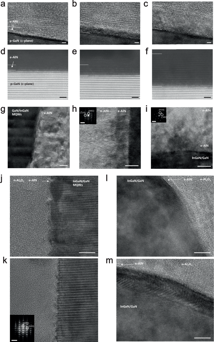
a–f HR-TEM (a–c) and atomic HAADF-STEM (d–f) images of e-AlN on c-plane GaN films with variable thicknesses of 0.8 (a, d), 2,3 (b, e), and 5.6 nm (c, f). g–i TEM images of the red InGaN/GaN nanorod LEDs coated with e-AlN (10 nm)/n-AlN (40 nm). g, h Vertical cross-sections near MQWs and n-GaN, respectively. i Horizontal cross-section near MQWs. Insets of (h, i), Corresponding SAD pattern. j–m TEM images of the red LED nanorods coated with e-AlN (~2 nm)/n-Al2O3 (48 nm). j, k Vertical cross-sections near MQWs (j) and n-GaN with FFT pattern (k). l, m Horizontal cross-sections near MQWs at two different locations. HAADF-STEM, HR-TEM, SAD, and FFT represent high-angle annular dark-field scanning transmission electron microscopy, high resolution TEM, selected area diffraction, and fast Fourier transform, respectively. Scale bars, 1 nm (a–f), 5 nm (g–m), and 5 nm−1 (Insets of e–g).
The critical shell thicknesses for wurtzite or zinc blende GaN/AlxGa1-xN and GaN/InyGa1-yN core/shell hetero-structure can be calculated17,18. Dislocation-free strain accommodation in the core-shell nano-structure that can effectively increase tcr, AlN is available only when the GaN core diameter is below ~10 nm. Therefore, in our case with the diameter of GaN nanorod core larger than 600 nm, tcr, AlN should be close to the bulk value of conventional film hetero-epitaxy, which is estimated to be ~1 nm. In case of AlN/In0.35Ga0.65N hetero-epitaxy in the red QW, tcr, AlN should be lower than 1 nm due to larger lattice mismatch. To verify the concept, we further in-depth analysed the structure of 2-nm-thick e-AlN on the InGaN/GaN MQW sidewall using atomic HAADF-STEM (Fig. 3a–e), which is able to distinguish heavy In or Ga atoms from light Al atoms by bright and dark contrast, respectively. As estimated, we can identify that AlN/GaN interface is fully coherent while, in the AlN/InGaN interface, there is a defective (low atomic ordering) region (Fig. 3a) or dislocation (Fig. 3b). Inspection of Fig. 3a, b shows the thickness of e-AlN is 5–7 atomic layers, corresponding to 1.5–2.1 nm. Interestingly, we observe dislocation in InGaN QW from the surface probably induced by e-AlN (Fig. 3c). We note that, due to the cylindrical shape of the nanorod, vertical cross-sectional observation often exhibits curved-edge artefact image unless the sampling thickness is thin enough (Fig. 3d and Supplementary Fig. 3a). Nevertheless, the atom-layer-thick line profile analysis, where only a single atomic layer is included with a width of 0.25 nm (Supplementary Fig. 3b), clearly reveals gradually decreasing oscillation amplitude abruptly decreases in the e-AlN region (Supplementary Fig. 3c). We can identify that e-AlN is 5-Al-atom-layer thick, corresponding to the thickness of AlN is ~1.5 nm, consistent with that in Fig. 3a, b. The atom-layer-thick line profile analysis might be useful to get rid of the artefact in the TEM analyses of ultrathin film on curved surface. On the other hand, horizontal cross-sectional TEM enables the curved artefact-free observation on ultrathin e-AlN (Fig. 3e), though it is somewhat difficult to identify point of interest. Moreover, energy dispersive spectroscopy (EDS) analyses compositionally verified the 2-nm-thick e-AlN on InGaN/GaN MQW sidewalls (Fig. 3f). It is reported that the required thickness of dielectric layer to determine its Qf to be fixed is 5 ALD cycle (~0.5 nm)19. We claim that 1- or 2-nm-thick e-AlN, with high crystallinity except presence of slight dislocation or defects near InGaN QW, is ideal chemical and physical passivation.
Fig. 3: In-depth atomic structure analyses of ~2-nm-thick e-AlN at MQW region.
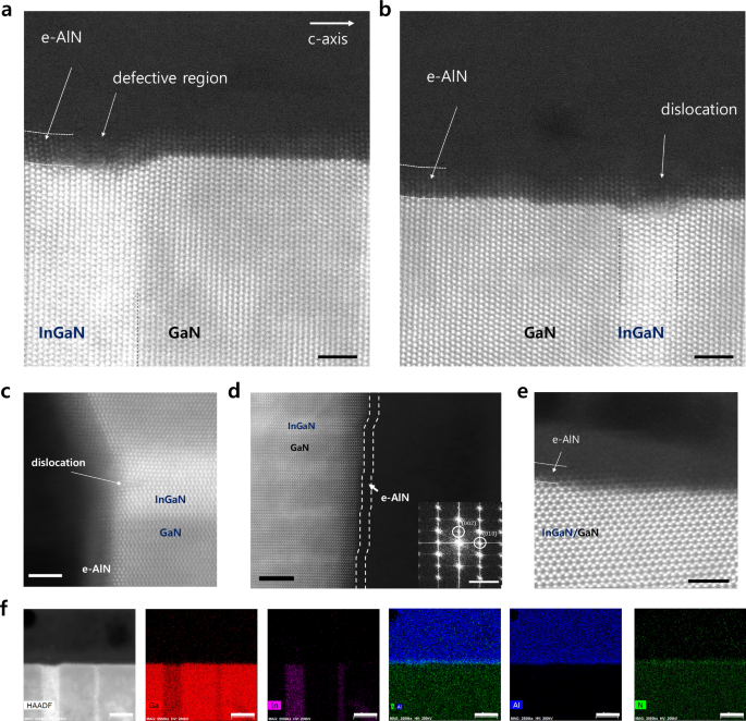
a–d Atomic HAADF-STEM images of the e-AlN. a–d Vertical cross-sections at different locations, showing AlN-(In)GaN hetero-epitaxy. a, b Conformal e-AlN with fully coherent epitaxy at e-AlN/GaN interface. At e-AlN/InGaN interface, defective (low atomic ordering) region (a) and dislocation (b) observed in e-AlN, marked by arrows. c Dislocation induced in InGaN marked by an arrow. d Conformal e-AlN on MQWs with thicker TEM sampling. (inset) corresponding FFT image. e, Horizontal cross-sections near MQWs. f (left) HAADF-STEM image. Next panels are corresponding EDS maps. Scale bars, 2 nm (a, b), 5 nm (c, d), 5 nm−1 (Inset of d), 1 nm (e), and 7 nm (f).
The epitaxial passivation effect itself was optically compared with other surface passivation including n-HfO2 and n-AlN for the InGaN/GaN nanorod LED arrays (diameter/pitch = 0.6 μm/1.8 μm). Fluorescence microscopy (Fig. 4a–d) revealed that the e-AlN passivation showed superior photoluminescence (PL) intensity and uniformity compared to that by n-AlN or n-HfO2. The PL intensity of the nanorod array obtained by epitaxial passivation was 2.5 times larger than that of n-HfO2 (Fig. 4e). We note that epitaxial passivation showed superior PL intensities over a wide thickness range (1–30 nm) as shown in Supplementary Fig. 4. We suggest that the first few nanometres of AlN determined the PL enhancement, while subsequent n-AlN or n-Al2O3 layers acted only as insulating layers for EL devices. It can be seen that the PL enhancement factor for epitaxial passivation was approximately 2.5 (Supplementary Fig. 4). We also compared the PL decay characteristics (τPL) for the same samples with time-resolved PL (TRPL, Fig. 4f). As shown in the figure, we obtained a fourfold increase in the τPL20,21 passivated by e-AlN compared to that passivated by n-HfO2 as summarized in Supplementary Table 1; this indicated enhancement of the internal quantum efficiency (“Methods”). Next, we prepared the red nanorod-LED arrays with more versatile passivation layers and compared their relative electroluminescence (EL) efficiencies (ηEL) in Fig. 4g. Fabrication flow of the nano-LEDs is described in Supplementary Fig. 5a with device structures (Supplementary Figs. 5b, c), exhibiting microscopically non-uniform colour/intensity variation (Fig. 4h). It is evident that most e-AlN/n-Al2O3 based nano-LEDs yields higher efficiencies than that of the control LEDs (n-HfO2/n-Al2O3 and n-AlN/n-Al2O3) for full range of the injection current, where n- Al2O3 (40–49 nm) is used for insulating the LEDs. This confirms beneficial influence of epitaxial passivation, consistent with optical data (Fig. 4d–f). As discussed in the structural analyses, the tAlN has striking effect on ηEL. In the range of tAlN of 0.5–2 nm, the ηEL of the nano-LED with e-AlN is drastically increased, ~2.5 times larger than that with n-HfO2 for the whole current injection range. The maximum ηEL is achieved at tAlN of 1 nm with slightly lower values at tAlN of 0.5 nm and 2 nm. However, at tAlN of 10 nm, ηEL decreases again significantly. The efficiency decrease with increasing tAlN is consistent with discussion in the structural analyses in Figs. 2 and 3, associated with high defect generation in the e-AlN much beyond tcr, AlN. On the contrary, there is very few thickness effect of e-AlN on the optical intensity (Fig. 4d–f), which is under investigation.
Fig. 4: PL and EL of red nano-LEDs with various ALD passivation layers.
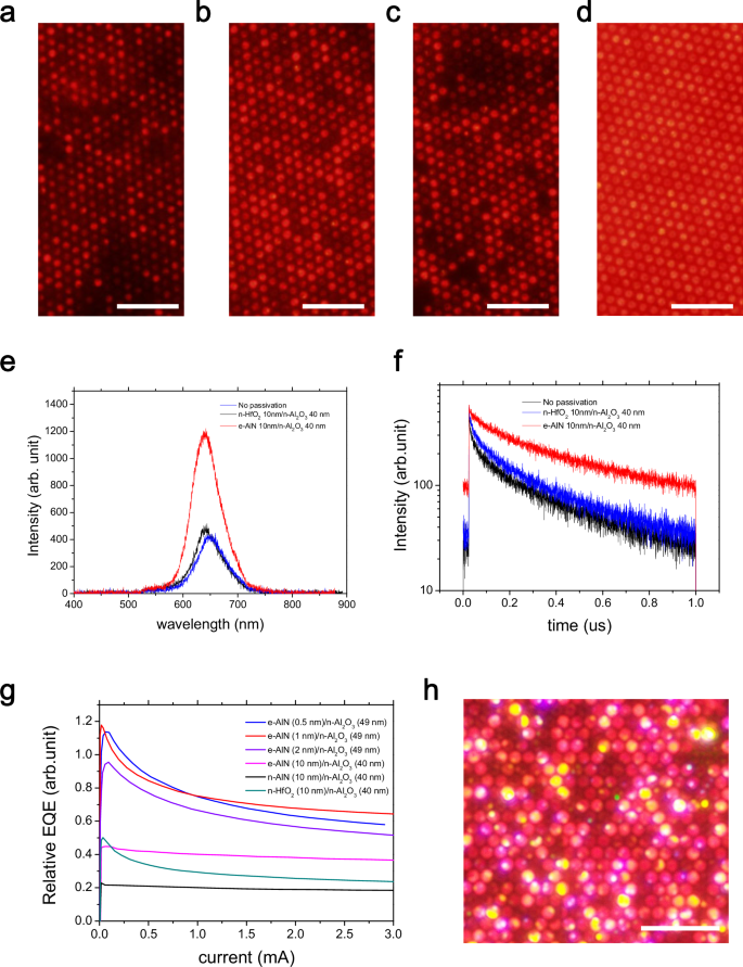
Fluorescence microscopy images of the as-dry/wet etched state (a), coated with n-HfO2 (10 nm)/n-Al2O3 (40 nm) (b), with n-AlN (10 nm)/n-Al2O3 (40 nm) (c), and with e-AlN (10 nm)/n-Al2O3 (40 nm) (d). e, f Time-resolved PL measurements. PL spectra (e) and decay time curves (f) using. g EL efficiency comparison of the nano-rod LEDs for various passivation layers. h Typical optical microscope image of the nano-rod LEDs. Scale bars, 10 µm (a–d, h).
By choosing the optimal e-AlN (e-AlN (1 nm)/n-Al2O3 (49 nm)) determined from Fig. 4g, we fabricated the flipped InGaN/GaN μ-LEDs (diameter/pitch = 1.5 μm/4.5 μm) for high efficiency, with detailed process flow in Supplementary Figs. 6a–i. We note that the fabricated red μ-LEDs (Supplementary Fig. 6j) seem to exhibit macroscopically uniform EL emission even at low current density of 0.24 A per cm2 and high brightness with increasing current (Fig. 5a and Supplementary Fig. 6k). However, we observe that there is still microscopic EL non-uniformity at low current densities in the range of 0.8–3.2 A per cm2 (Fig. 5b). Considering that even the e-AlN passivated nano-LEDs show quite uniform PL intensity (Fig. 4d), we attribute the EL non-uniformity of the μ-LEDs to non-uniform current injection. To address this issue, we are investigating the non-uniform ohmic ITO contact with p-type GaN. It should be mentioned that the non-uniform current injection is much stronger in nano-LEDs. Inspection of Fig. 4h reveals local pink colour, mixture of red and blue peaked at ~460 nm (Fig. 5d), suggesting strong localized current injection. This strong colour variation/localized current injection in nano-LEDs could be associated with randomly distributed V-pit defects of comparable size to nano-LEDs, which are commonly observed in red epitaxial layers. For the larger diameter μ-LEDs, microscopic colour variation is significantly reduced probably due to decrease in V-pit induced local current injection effect (Fig. 5b).
Fig. 5: EL of red InGaN/GaN μ-LEDs with e-AlN (~1 nm)/n-Al2O3 (49 nm).
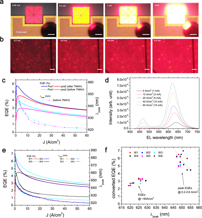
a Low-magnification optical microscope (OM) images in the current range of 0.06–5 mA. b High-magnification OM images in the current range of 0.2–0.8 mA. c EQE and peak wavelength (λpeak) curves vs. current density (J) before and after roughening with tetramethylammonium hydroxide (TMAH). d Corresponding emission spectra of the cyan curve in left panel. e EQE and λpeak curves vs. J for four different wafers after the TMAH roughening. f Converted EQE vs λpeak relations at current densities of maximum EQE and of ~40 A per cm2 for six different samples (18 points), including samples in (e). Scale bars, 200 µm (a) and 20 µm (b).
The flipped μLEDs, without applying encapsulating polymer, are designed to also maximize the extraction efficiency (EE) by surface roughening and adequate placement of Al reflection layer (Supplementary Fig. 6i). It was found that surface roughening achieved by the TMAH wet treatment increases the EE by ~1.5 times (Fig. 5c). Despite the EQE variation depending on the wafer position, the peak absolute EQE of red μ-LEDs is 5.8% at the peak wavelength (λpeak) of 645 nm and the current density of ~1 A per cm2 (Fig. 5c), measured by integrating sphere (“Methods” and Supplementary Fig. 7). The EQE is ~3.1% even at relatively high current density (J) of 40 A per cm2. As spectral broadening and blueshift is inevitable like other green/red InGaN LEDs with blue side peaks (Fig. 5d), absorption type filter would be required for display application. To investigate wafer to wafer variation, we have further measured absolute EQE and λpeak for four different wafers with slightly different emission characteristics (Fig. 5e). For #1-#3 wafers, the peak EQEs were 6.1–7.0% with λpeak of 646–649 nm at J of 0.2–0.8 A per cm2. The median EQE of 6.5% with λpeak of 649 nm is shown in the cyan curve in Fig. 5e and Supplementary Fig. 6l. To our knowledge, this red EQE value has been significantly improved for μ-LEDs of such a small diameter of 1.5 μm. On the other hand, for #4 wafer, relatively low peak EQE of 4.5% is observed with λpeak of 653 nm at J of 2.0 A per cm2. Considering its high initial λpeak of 670 nm at J of 0.2 A per cm2, which is 11–16 nm larger than those of #1-#3 at the same J, it is estimated that #4 has higher indium concentration (x) in InxGa1-xN QW. This explains the observed low EQE due to increased defects in the high x QW. At J of 40 A per cm2, absolute EQEs exhibit smaller variation in the range of 2.8–3.3% (Fig. 5e). It should be mentioned that the EQE convergence into the narrower range at high current density is attributed to the fact that Auger recombination dominates the droop characteristics of the μ-LEDs22,23. To improve EQE uniformity and droop characteristics, optimization of the InGaN LED epitaxial film is also needed. We get statistical data on EQEs of 18 points (six different wafers, including four wafers in Fig. 5e and 3 different points per wafer) using the spectra-radiometer. (Fig. 5f) The spectro-radiometer measures optical power for the given solid angle to calculate relative EQE, which we convert to absolute EQE by multiplying the conversion factor, as described in “Methods” and Supplementary Fig. 7. The peak converted EQEs at J of 0.3–2 A per cm2 were 4.5–7.0% with λpeak of 646–649 nm, and the converted EQEs at J of 40 A per cm2 were 2.2–3.4% with λpeak of 619–629 nm, exhibiting the similar tendency as in Fig. 5e. As explained, there is decreasing tendency of the peak EQE with increasing peak wavelength, marked by a dotted line in Fig. 5f.
Near complete transfer for flexible micro-LEDs
In this section, we demonstrate flexible inorganic UHD displays with their fabrication scheme shown in Fig. 6a–c; it can transfer red μ-LEDs, called a near-complete device. As described in Supplementary Fig. 8 and “Methods”, the fabricated near-complete device is flipped and bonded to a PI-coated glass substrate with an adhesive polymer (Fig. 6a), followed by removal of the growth substrate (Fig. 6b). The transfer scheme has the distinct ability to facilitate the peel-off-free removal of the Si growth substrate, which is inherently controlled by the interface strength. When we divide the total grinding force (F) during mechanical removal of the Si substrate into the normal grinding force Fn and tangential grinding force Ft, we see that peel-off of the PI film occurs during mechanical grinding only if Ft is larger than the adhesion strength or force (G) of the PI (flexible substrate)/glass (carrier substrate) interface, Ft > G. In the suggested fabrication scheme, the above condition can be satisfied spontaneously; therefore, peel-off rarely occurs during grinding, as described below. Ft monotonically increases with increasing wafer rotation speed, which increases the abrasive wheel feed rate and decreases the wheel rotation speed24. On the other hand, systematic steered molecular dynamics simulations were used to show that G also increased with sliding speed25. It was also reported that the absolute value of G was maintained at a high level with a moderate choice of PI with higher stiffness and low thermal expansion coefficient and by controlling the processing parameters such as UV radiation or PI curing time26. These studies explain why the devised scheme is highly robust. In other words, Ft and G increase together with increasing sliding speed while holding Ft < G, which makes the process invulnerable to grinding parameters, including the wheel or wafer rotation speed. This peel-off-free removal with a large process window will be verified in the following sections. Low-alignment-accuracy post processing, including the common electrode to the n-GaN (N-comm) and pad opening, finalizes the flipped, near-complete device, which becomes flexible via excimer laser lift off (LLO, Fig. 6c), as described in the “Methods”. With the detailed fabrication flow (Supplementary Fig. 8), we verified flexible red μ-LEDs. It can be seen that the flexible μ-LEDs maintain highly efficient, bright, and macroscopically uniform EL emission both in the middle of the release step (Fig. 6d, e) and in the fully released flexible form (Fig. 6f, g).
Fig. 6: Near-complete device transfer for flexible e-AlN passivated red μLEDs.
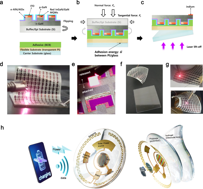
a–c Schematic fabrication flow. a Flipping of the red μLEDs to enable adhesive bonding on PI/glass. b Epi-wafer removal by controlling the interfacial forces and subsequent n-GaN removal. c Postprocessing including pad electrode formation, and laser lift-off. d, e Operation of flexible red μ-LEDs in the middle of the release step; photograph (d) and microscope image (e). f Photograph image of released μ-LEDs from a carrier glass substrate corresponding to (c). g Photograph images of flexible red μ-LEDs operating under fully flexible forms. h Conceptual schematic for an electronic contact lens with a flexible display. A scale bar, 200 µm (e).
For the reader’s reference, we have also demonstrated flexible 5000 ppi displays using the planar blue InGaN μ-LEDs pixelated by ion implantation3,27,28. We show three changeable still images (zebra, checker, and gradation) at the selection of VDD1, VDD2, and VDD3 with the corresponding pad electrodes (Supplementary Fig. 9). This is achieved by designing the unique TFT-free structure on the planar blue μ-LEDs with the selective Via1 opening pattern, as described in the “Methods” and Supplementary Fig. 10a–m. The TFT-free assembly can be transferred onto a PI/glass substrate, post-processed, and released into a flexible form. Supplementary Fig. 10w shows the robust interfaces formed after the transfer. The released flexible displays, with a total thickness of less than 20 μm, exhibited stable electroluminescence (EL) spectra (Supplementary Fig. 9c), and defect-free, changeable still images at variable bending forms (bottom panels of Supplementary Fig. 9a). This 5000 ppi pixel density was verified by optical microscopy images at the fixed location with various magnifications (Supplementary Fig. 9d). We expect that the mesa-etched red InGaN μ-LEDs, once flattened by chemical mechanical polishing, can also be integrated into the UHD display using the same fabrication process (Supplementary Fig. 10n–v). We believe that with the development of monolithic integration of both high-mobility channel-based TFTs and RGB μ-LEDs, the described structure will evolve into a monolithic flexible UHD full-colour μ-LED display. We hope that this will pave the way for electronic contact lens29, an eventual form factor for near-eye display (Fig. 6h). Lastly, we describe our preliminary progress on monolithic TFT integration and lens assembly in the supplementary information (Supplementary Figs. 11–17).
We have demonstrated 1-nm-thick e-AlN passivation of 1.5 μm diameter μ-LEDs with the EQE of 6.5% at 649 nm by developing Ar plasma heating-based ALD. The e-AlN passivation almost perfectly passivates the tiny red μ-LEDs with conformal thickness of 1 or 2 nm, as verified by HAADF-STEM analyses. We then have demonstrated flexible red InGaN μ-LEDs by developing the near complete device transfer process. By breaking the red spectral efficiency and form factor bottlenecks for inorganic μ-LEDs, we believe our study can provide a paradigm for highly efficient, flexible UHD RGB displays that can expand the range of AR applications, including electronic contact lenses.
Methods
Fabrication of red nano and micro light emitting diodes
We fabricated InGaN-based red nano LED (diameter (D): 0.65 μm/height (H): 4.3 μm/pitch (P): 1.8 μm) and μ-LED (D: 1.5 μm/H: 2.0 μm/P: 4.5 μm) arrays, As the subpixel pitch of 5000 ppi (pentile) is 2.5 μm × 5.0 μm, both nano-LEDs and μ-LEDs can easily extend into >5000 ppi. Red LED epi-layers (p-GaN/p-AlGN EBL/InGaN-GaN MQWs/InGaN-based buffer/n-GaN/u-GaN) are prepared on 8-inch, 1.5-mm-thick silicon wafers (epi-wafer), details of which are beyond the scope of this paper. ITO (100 nm) sputtering for p-GaN electrode, PECVD SiO (1.0 μm)/sputtering Al (200 nm) for hard mask of GaN etching are successively deposited on the epi-layers, then patterned with nano-LED and μ-LED array. Through the SiO2/Al pattern, ITO/GaN epi-layers were mesa-etched by inductive coupled plasma etching using an Ar/Cl2 mixture, and its height was easily controlled by adjusting the etching time. The plasma damage at the etched surface was removed by wet chemical treatment (KOH or TMAH). On the wet chemically treated nanorod array, a surface passivation/insulation layer was deposited by ALD. The epitaxial passivation consisted of a 0.5–10-nm-thick epitaxial AlN/40-nm-thick normal amorphous AlN, Al2O3, or SiO2 shell, while the control passivation consisted of a double amorphous layer of 10-nm-HfO2 (thermal)/40-nm-Al2O3, similar to that reported in ref. 5 (Fig. 1e and Supplementary Fig. 1a). A e-AlN passivation layer was deposited on the nanorod array by Ar plasma heating-assisted ALD, in which Ar plasma (450 W, 40 s) heating was performed after every 4 ALD growth cycles, followed by an amorphous layer including AlN, Al2O3, or SiO2 using conventional ALD processes. The parameters for the Ar plasma, including the insertion period, plasma power, and time, were optimized to secure a flat morphology for the epitaxial AlN layer while maintaining the epitaxial quality. For example, insertion after the 1-ALD cycle showed an epitaxial relationship with a rough film morphology, while insertion after the 6-ALD cycle resulted in a loss of the epitaxial relationship. On the other hand, the Ar plasma power/time mainly affected the crystallinity of the epitaxial layer. A low power resulted in low crystallinity, while a high power caused plasma damage.
The structure of nano-LEDs is un-flipped (epi-up, Supplementary Fig. 5). After depositing passivation layers on nano-LED arrays, opening of ITO p-electrode is performed by etching of the passivation layer by CF4/Ar/O2 plasma. Next, the arrays are coated with photoresist for insulation, followed by O2 plasma again to open the ITO electrode. Finally, shadow-masked SiO2/Ti/Au evaporation is performed for metal contact electrode, and shadow-masked ITO sputtering for spreading p- electrode. N-electrode contact is done by the sidewall of the wafer.
The structure of μ-LEDs is flipped (epi-down, top panel of Supplementary Fig. 6i). Up to the flipping stage, the fabrication process is basically the same as for nano-LEDs. Here, photoresist insulation layer is replaced by SiO2 (100 nm), sputtered ITO p-spreading electrode by ALD ITO (50 nm). An evaporated Ti (5 nm)/Au (100 nm) pattern is used as p-metal electrode. The patterning is done by conventional lithography. The fabricated μ-LEDs are electrically tested for light emission, followed by flipping process using adhesive bonding as follows. The red μ-LEDs on the Si epi-wafer are coated with PECVD-SiO2 (100 nm), then bonded to a polyimide-coated glass substrate (a receptor) with an adhesive resin (benzocyclobutene (Dow Chemical)) (Fig. 6a and Supplementary Fig. 6e). Only for testing EL performance, the receptor was prepared with aluminium/SiO2 coated slilcon wafer (Supplementary Fig. 6). And for flexible uLEDs (Supplementary Fig. 8), the receptor was prepared with 0.7-mm-thick transparent glass wafer (Corning, Eagle glass X) spin-coated (300 rpm, 30 s) with varnish (IPITECH Inc.) to form a ~12-μm-thick PI layer as the flexible substrate, cured in N2 and heated with the profile 150 °C 10 min–200 °C 10 min–250 °C 10 min–300 °C 10 min in series. The 1.5-mm-thick silicon epi-wafer was first removed via diamond mechanical polishing (DMP) down to 80–100 μm and finally via high-speed silicon reactive ion etching of the substrate (Fig. 6b). For DMP, we found that a wheel feed rate of <150 (μm per min), wheel speed of <5000 rpm, and wafer rotation speed of <400 rpm successfully achieved stable substrate removal without any peel-off of the spin-coated PI film. The typical grinding process was performed in two stages: wheel feed rate of 1st stage: 1.5–2 μm per sec; 2nd stage: 0.5 μm per sec, wheel speed of 1st: 1500 rpm, 2nd stage: 2800 rpm, and wafer rotation speed of 1st: 250 rpm, 2nd stage: 150 rpm. After Si wafer removal, the AlGaN-based buffer and some of the n-GaN layers were etched with a flood-area inductively coupled plasma (Cl2/Ar) down to an n-GaN thickness of ~3 μm. Then, ITO/Au p-GaN pad electrode is open through forming n-GaN hole using Cl2/Ar plasma etch of n-GaN (top panel of Supplementary Fig. 6h and Supplementary Fig. 8d), finalizing transfer. At this stage, the transferred flipped μ-LEDs is electrically tested for EQE, I-V-L measurements. For flexible displays, the μ-LEDs on PI coated glass were released by excimer LLO (Fig. 6c and Supplementary Fig. 8c). LLO was performed by raster scanning with an excimer laser at a wavelength of 308 nm onto the backside of the transparent receptor; the repeat rate was 10 Hz, the shot overlap was 70%, and the energy density was 130–140 mJ per cm2. Under these conditions, the decomposition of polyimide at the polyimide/glass interface was reproducible.
Fabrication of flexible micro light emitting diode displays
The actual fabricated μLED display was TFT-free but specially designed (Supplementary Figs. 10a–e) to show three different still images with the same layer structure as that of the TFT except for the active layer (Supplementary Fig. 10f). After pixelation of InGaN blue epilayers by Ar+ ion implantation3 (an energy of 5 keV and a dose of 2 × 10¹² per cm2), Ni (5 nm)/ITO (100 nm) was evaporated with an e-beam and lifted off to form a p-GaN electrode with a rectangular pixel shape. Then, 300-nm-thick SiO2 was PEDCVD-deposited as the first insulator (Ins1), followed by selective openings in Ins1 (Via1) containing three different encrypted images by Boolean operation of real image data and all of the pixel openings. We note that the pixelation by mesa-etched InGaN red μ-LEDs can also be applied using essentially the same process flow except additional chemical mechanical polishing (Supplementary Fig. 10n–v). Then, 180-nm-thick molybdenum (Mo) was sputter-deposited and patterned as the first metal layer (M1). Through Via1, M1 and p-electrode are interconnected. Then, 300-nm-thick SiO2 was deposited as the second insulator (Ins2), followed by openings in Ins2 (Via2). Via2 having periodic openings in Ins2 through which M1 and M2 connected in the X-Y matrix form, uniformly delivered three VDD’s to corresponding p-electrodes. In short, the device consists of monolithically formed/Ins1 and Ins2 and M1 and M2 on pixelated InGaN μ-LEDs. The three changeable images are displayed by selectively delivering VDD1, VDD2, and VDD3 to the respective p-GaN electrode (PE) through the selective Via openings to form near-complete device (Supplementary Fig. 10d). Then, the near-complete device was transferred into the PI/glass substrate by the described adhesive bonding, followed by the common electrode to n-GaN (N-comm) and opening of p-pads (Supplementary Fig. 10e) with a cross-sectional schematic (Supplementary Fig. 10m). The flexible μ-LED display was released by the same LLO method.
Optical and electrical measurements of nano and micro-LEDs
Fluorescence microscopy was used to characterize the photoluminescence characteristics of the nanorod arrays for various passivation treatments. For quantitative comparison to determine whether a 2.5-fold enhancement was observed, microscope images were obtained at two different exposure times of 200 ms and 500 ms and compared with the blue rectangles marked in Supplementary Fig. 4.
The PL decay times (τPL) for the nanorod LED were obtained for the same samples after different passivation conditions with time-resolved photoluminescence (TRPL). Based on the excellent fit to a biexponential decay shape, we obtained decay times with fast and slow components of τ1 and τ2 (Fig. 4f) and amplitudes of A1 and A2. The average decay time (τPL) was calculated with the relation ?PL=?1?1+?2?2?1+?2. τPL (256 ns) for the epitaxially passivated nanorods was significantly larger than those (60–65 ns) of untreated or normally passivated nanorods, as summarized in Supplementary Table 1. In addition, the internal quantum efficiency (?int) of the red nanorod array is expressed by the following equation.

where τr and τnr are the radiative and nonradiative lifetimes, respectively. Here, we assume τnr ~ τPL at room temperature and the relationship 1/τPL = 1/τnr + 1/τr ~1/τnr. With the enhanced τPL assuming a fixed τr for the same InGaN epilayer, the internal quantum efficiency (?int) of the nanorod array is expected to be greatly increased by epitaxial passivation.
The absolute EQEs of red μ-LEDs in Fig. 5c and e are directly measured by integrating sphere (ISP-75, Instrument Systems Inc.). I-V-L (current-voltage-luminance) characteristics of red nano-LED/μ-LEDs are obtained by spectro-radiometer (CS-2000, Konica-Minolta Inc.). Due to difficulties of wiring into p-pad electrode using integrating sphere, we obtained statistical data of EQEs/peak wavelengths from the spectro-radiometer (Supplementary Fig. 7) using the following conversion procedure. First, we measured absolute EQEs for only 4 points (4 wafers) using an integrating sphere in Fig. 5e. Next, using a spectro-radiometer, we measured optical power for the given solid angle, and calculated relative EQE for the same 3 points in Fig. 5e, assuming a Lambertian angular distribution. We obtain an average conversion factor of 1.48 by dividing the absolute EQE by the relative EQE curves (Supplementary Fig. 7). We then get relative EQEs for total 18 more points from six wafers including 4 wafers in Fig. 5e, which are converted to absolute EQEs (converted EQEs) to show statistical data in Fig. 5f. The microscopic EL images are obtained by long-focal-length optical microscope equipped with micro-probe giving DC voltage to transferred red μ-LEDs or blue UHD displays.