


Abstract
Full characterization of light intensity, polarization, and spectrum is essential for applications in sensing, communication and imaging. However, existing schemes rely on discrete, bulky components to capture polarization and spectrum separately, and suffer from detecting only a few values in each dimension. Here, we implement a compact disordered-guiding photonic chip with a neural network for single-shot high-dimensional light field detection. The disordered region introduces complex interference and scattering among polarized components, while the guiding region efficiently collects the outputs to on-chip photodetectors. This design encodes high-dimensional input into multi-channel intensities with high sensitivity, subsequently decoded by the neural network. Experimentally, the accurate detection of broad spectrum with mixed full-Stokes polarization states is realized with a polarization error of 1.2° and spectral resolution as high as 400 pm. Furthermore, the device demonstrates high-dimensional imaging with superior recognition performance over single-dimensional methods. This innovation offers a compact and high-resolution solution for high-dimensional detection.
Introduction
Intensity, polarization, and spectrum of light, as distinct dimensional characteristics, provide a comprehensive understanding of light-matter interaction and are crucial across nearly all domains of optical science and technology1,2,3,4. For instance, the polarization information5 is critical for determining material composition and surface texture, whereas spectral analysis is instrumental in medical diagnosis and wavelength-division optical communication6. As modern technology rapidly advances, the demand for comprehensive detection of high-dimensional light field continues to grow7,8.
Conventional detection devices typically measure either spectrum or polarization of input light, sacrificing the valuable information from other dimensions. A common solution is to incorporate multiple discrete diffraction elements and optical filters to separately distinguish light with different polarization and wavelength9,10,11,12. However, this leads to bulky and time-consuming systems. Recently, several integrated high-dimensional detectors based on optical metasurfaces13 have been proposed, and the typical representative relies on mapping different dimensional information into distinct locations, using position and intensity distributions for light field detection14,15. However, as the number of detection parameters increases, the signal crosstalk between different information at different spatial locations become pronounced16,17,18. Another type of detector, based on computational reconstruction, maps light field into a series of outputs, encoding the entire high-dimensional information rather than isolating individual dimension19,20,21,22. Nevertheless, these systems are generally restricted to detecting light fields at a few values with low resolution in each dimension, such as limited polarization and wavelength channels, due to the limited internal degrees freedom in the encoding devices23,24. Additionally, most of them rely on commercial cameras, inevitably requiring numerous detector arrays25. Consequently, achieving fully high-dimensional characterization of arbitrary complex light field with a compact and efficient system remains challenging.
In this work, we propose and demonstrate an on-chip high-dimensional detection system capable of characterizing broadband spectrum along with arbitrary varying full-Stokes polarization through single-shot measurement. The high-dimensional input is encoded into multi-channel intensities through the uniquely designed disordered-guiding chip, and decoded by a multilayer perceptron (MLP) neural network (Fig. 1). The core disordered region introduces complex interference between two separate orthogonal polarization components and multiple scattering to enhance the dispersion effect, enabling rich polarization and spectrum responses. Whereas, the surrounding guiding region based on inverse-design directs the input light to the on-chip photodetectors (PDs), improving the transmittance and detection efficiency. With the assistance of neural network for decoding, we achieve reconstruction of full-Stokes polarization and broadband spectrum with a single measurement. It reveals a high spectral sensitivity of 400 pm with average spectral error of 0.083, and polarization error of 1.2°. Furthermore, we demonstrate a high-dimensional imaging system, exhibiting superior imaging and recognition capabilities compared to conventional single-dimensional detectors. This demonstration holds promising potential for future imaging and sensing applications.
Fig. 1: The principle of proposed high-dimensional detection and imaging system.

The image of an object (e.g., a five-point star), which carries unknown polarization and spectral information at each pixel denoted as ?(?0?1?2?3?), is encoded as multi-channel photocurrents by a disordered-guiding chip. The disordered-guiding chip comprises a fully disordered scattering medium surrounded by inverse-designed ordered guiding region. The two orthogonal polarization components (?? and ??) undergo complex interference and scattering within the chip, generating multiple outputs sensitive to both polarization and wavelength. The output multi-channel photocurrents ?(?0?1?2?3?) from a PD array are then decoded with a post-processing neural network. Once the high-dimensional polarization and spectral information of each pixel is reconstructed, denoted as?^(?0?1?2?3?), the full-Stokes spectral image of the original object can be recovered.
Results
Principle and design of the disordered-guiding photonic chip
We design and fabricate the high-dimensional detection chip on a silicon-on-insulator (SOI) wafer (Fig. 2a). The input light is firstly split into the horizontal component Ex and the vertical component Ey, through a polarization beam splitter-rotator (PSR). The dual beams, carrying the complete polarization-dependent amplitude and phase information, are then injected into a disordered-guiding medium (Fig. 2b). Within the disordered region26, the two orthogonal polarization components interfere, with the resulting intensity determined by their relative amplitude and phase that directly tied to the input polarization state27,28. Strong scattering within the region further amplifies dispersion effects, enabling each wavelength to generate a distinct output pattern. For broadband light, the output represents a superposition of the characteristic responses of individual wavelengths. Consequently, output intensities of the chip provide a sort of fingerprint, uniquely identifying the polarization and spectrum of the input signal. Each output intensity is a weighted sum across the entire spectrum, incorporating the response of each wavelength channel and polarization. Therefore, the intensity at the l-th output can be described as:

where ????(?=0,1,2,3) represents the transmission coefficient for different Stokes polarization components at the i-th wavelength channel, and ??? is the different Stokes polarization components of input information from each pixel of the object at the i-th wavelength channel. Furthermore, we represent the mapping responses of the entire device in the form of a transmission matrix:

where ???0,???1,???2,???3 is the l-th row of analysis matrix29 (see Note S1), ? is the number of output port and n denotes the number of wavelength channels. By utilizing on-chip germanium-silicon (Ge-Si) PDs30,31 for photoelectric conversion, the multi-channel output photocurrents can be expressed as ?=?⋅???, where ? represents the responsivity of PD (Fig. 2c). These characteristic photocurrents are then decoded by the neural network for the extraction of full-Stokes polarization and spectrum information, with the mapping relationship ?(?1?2???).
Fig. 2: The structure and design of the disordered-guiding chip.

a The microscopy of the disordered-guiding chip. b The horizontal component Ex and the vertical components Ey are injected to the disordered-guiding medium, with two inputs and sixteen outputs. c The Ge-Si PD is used to converted the optical output to photocurrent signal. d The correlation coefficient under different hole diameter and number. e The transmission spectra of the 16 outputs exhibits significant differences and decorrelation at different input polarization states.
In the disordered region, randomly distributed air holes are etched into the silicon waveguide layer, where the hole diameter and density determine the scattering intensity and directionality. These factors alter the effective optical path length and transmission matrix, thereby influencing the high-dimensional responses of the device and detection resolution. The disordered medium employs 16 outputs to provide a compressed representation32,33 of the high-dimensional light field, balancing detection resolution and sensitivity while maintaining a compact footprint. To ensure high fidelity in polarization and spectrum detection, the correlation of all output responses at each wavelength channel should be minimized, allowing the system to distinguish variations in both spectral and polarization states. We evaluate this by calculating Pearson correlation coefficients34,35 across wavelength channels for different polarization states (see Note S2), where lower values indicate stronger decorrelation. Numerical simulations across different structural parameters show that the medium with 1500 holes and hole diameter of 160 nm (filling factor of 10.5%) results in the lowest average correlation coefficient across the spectra range of 1540–1560 nm (Fig. 2d). This ensures that the 16 output channels exhibit distinct transmission spectra under different polarization states, as seen in variations of peak positions, relative intensities, and spectral shapes (Fig. 2e).
In addition to detection resolution, sensitivity is another critical performance metric for high-dimensional detection systems. High sensitivity requires maximizing the transmission from the input waveguide through the disordered region to the PD. Although strong scattering enhances the sensitivity of the outputs to input information, some light leaks out from the outer edges of the disordered region. This leakage reduces the overall transmission efficiency and degrades the reconstruction quality. To address this issue, we introduce an inverse-designed36,37,38 light-guiding waveguide surrounding the disordered region to effectively capture the leaked light and orderly guide it into its corresponding port. The optimization function is defined as the average power across all ports over the entire wavelength range (see Note S3). The initial transmission efficiency of the device is quite low, and after six iterations, the transmission increases to 1.7 times the initial value (Fig. S3). Moreover, the integrated on-chip PD exhibits low noise characteristics, with an average dark current of 3.34 nA and responsivity of 1.05 A/W, ensuring stable and robust signal acquisition (see Note S4).
Single-dimensional polarization and spectrum detection
Although the output features are highly correlated with both polarization and spectral information, extracting multiple parameters from these features remains challenging. Directly modeling the output response to match experimental data is impractical due to the complex interference and scattering within the disordered-guiding medium. Pre-calibration with known incident light is unrealistic, as the continuous nature of polarization and spectrum leads to an infinite number of input possibilities. By contrast, neural network is well known for its ability of completing complex task without the need for prior knowledge23,39.
To validate the function of our system, we separately investigate its polarization and spectrum detection capabilities. For polarization detection, the input wavelength is fixed at 1550 nm and a polarization controller (PC) along with a commercial polarization analyzer (PA) are used to record distinct polarization states. 85 random polarization states, distributed in different positions of the Poincaré sphere are selected for the datasets. To ensure a rigorous evaluation, we split the dataset into 70%/10%/20% for training, validation, and testing, ensuring that no overlap exists between these subsets. Each spectral set consists of 10 independent measurements at different time instances, incorporating natural noise fluctuations. The model is optimized using the mean square error (MSE) of the polarization and spectrum prediction as the loss function, showing a steady decrease during training (Fig. 3a). For accuracy assessment, the polarization detection error is defined as:ε?=arccos?(?1?1′+?2?2′+?3?3′)/?0?0′. For an intuitive error analysis, we plot the predicted Stokes parameters against the reference input (Fig. 3b). The average polarization error is found to be 1.2° across all test data. Given that ?0 represents the optical power, the average optical intensity reconstruction error is also calculated to be 0.012 (Fig. 3c).
Fig. 3: The performance of full-stokes polarization and spectrum detection.
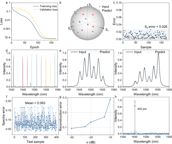
a The training and validation loss curves of the polarization detection regression task during the training. b Poincaré sphere representation of polarization states from the MLP model prediction (blue sphere) and the commercial PA. All the Stokes parameters are normalized by the optical power ?0 for clarity. c Predicted power ?0 error at different polarization states (gray dots). The intensity error of all testing samples is less than 0.026 (light blue shadow) and the average error is calculated to be 0.012. d Reconstructed spectra for a series of narrowband spectral lines across the 20 nm bandwidth. The dashed lines mark their center wavelengths of each peak. e Reconstructed spectra for continuous, broadband signals: the ASE source filtered by the PF with different wave shapes. f Reconstructed spectra for continuous, broadband signals: the ASE source filtered by the PF with different wave shapes. g The measured spectra reconstruction mean error under different noise factor σ ranging from 0.1 (-10 dB) to 0.001 (−30 dB). h Reconstructed spectra for dual spectral lines: dual peaks at 1545 and 1545.4 nm, with a spectral spacing of 400 pm.
Subsequently, the spectrum detection capability of the device is characterized. A broadband light source, programmable wavelength filter (PF), and commercial spectrometer are used to generate and record different input spectra at a fixed horizontal polarization. The wavelength range is set between 1540 and 1560 nm, divided into 201 channels (0.1 nm spacing per channel). After training, the predicted results of network are compared to those from the commercial spectrometer, defining the spectrum detection error as:ε?=||??????−????????||1/||??????||1. Several single-peak spectra are reconstructed, with an average detection error of 0.083 (Fig. 3d). Additionally, we demonstrate the reconstruction of continuous broadband spectra reconstruction, which is widely recognized as a more challenging task. Representative examples demonstrate minimal deviation from the reference input, confirming the stability and effectiveness of trained model across diverse spectral conditions (Fig. 3e). We test the model against random, previously unseen broad spectra, achieving an average reconstruction error of 0.083 (Fig. 3f). Additionally, to further evaluate the robustness of our system, we assess its performance under varying noise levels by introducing artificial Gaussian noise (noise factor σ ranging from 0.1 to 0.001). Through the noise-adaptive training strategy, the system maintains stable performance under certain noise conditions (Fig. 3g). To further validate the spectrum resolution, the dual-peak spectrum reconstruction train and test are conducted. The peak separation with 400 pm (1545 and 1545.4 nm) is well-distinguished, demonstrating a high resolution of 400 pm according to Rayleigh criterion40,41 (Fig. 3h). Details of the experimental setup and neural network training are provided in Note S5.
High-dimensional light field detection and imaging
Building on the single-dimensional detection capability for full-Stokes polarization and broadband spectrum, we subsequently demonstrate high-dimensional detection for broadband light carrying mixed arbitrary polarization states. A broadband beam carrying diverse polarization states is synthesized by controlling polarization and waveshape in multiple paths of light, and the collected photocurrents from the 16-channel PDs are used to train a neural network. Details of the experimental principle and setup are provided in Note S6. After normalizing the Stokes parameters to the maximum S0 over the entire wavelength range, the reconstructed full-Stokes spectrum is shown in Fig. 4a, b, which are compared with the reference input measured by commercial spectrometer and PA. It is evident that the predictions of neural network for polarization states and spectrum closely align with the reference input, with the spectral detection error of 0.082. We represent the Stokes polarization parameters error at each wavelength channel, all of which are less than 0.064 (Fig. 4c).
Fig. 4: High-dimensional light field detection and imaging.
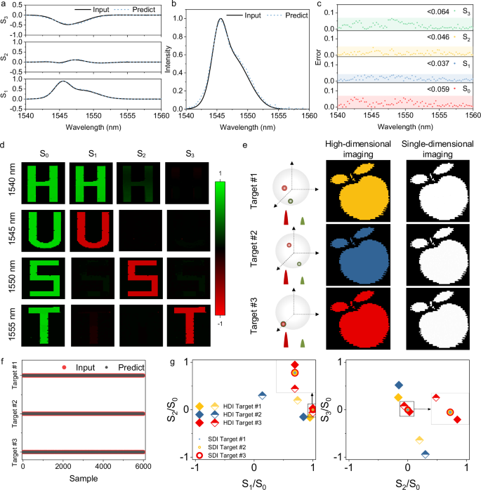
a Full-Stokes polarization spectra of broadband light source (with wavelength range from 1540 to 1560 nm under mixed random polarization) measured with the disordered-guiding chip (blue dashed lines) and bulky commercial devices (black solid lines). b Comparison between the reconstruction spectrum and the reference input. c The errors of the Stokes parameters over broadband wavelength range. d Reconstructed images of four “HUST” letters with different single-wavelength and polarizations. e High-dimensional imaging (HDI) and conventional single-dimensional imaging (SDI) results for “apple” masks. f The classification results of high-dimensional chip detection signals processed by the neural network, corresponding to the three targets. g The results for HDI and SDI under different inputs in the S1-S2 and S2-S3 planes. Solid diamonds and hollow diamonds represent the polarization states at 1550 and 1555 nm, respectively, with different colors indicating three targets. The circle denotes the detection results of a single-dimensional polarization imaging system. The polarization superposition states of three light fields are the same, and cannot be differentiated.
It is worth noting that to accommodate different detection tasks, we employ MLP models of varying architecture. Compared to simple single-dimensional reconstruction, broadband spectra with arbitrary polarization reconstruction involves higher output dimensions and more complex nonlinear relationships. Therefore, a deeper and wider network, along with stronger constrain strategies, is required to enhance the generalization capability of the model. In addition, the light field detection tasks fundamentally involve mapping between photocurrents and light field vectors rather than processing spatially structured data (as in convolutional neural networks) or sequential dependencies (as in recurrent neural networks), making MLP models particularly well-suited. We compared the performance of three network architectures in complex high-dimensional detection tasks. The results show that MLP not only achieves higher accuracy but also outperforms other models in both training and inference speed, maintaining computational efficiency (see Note S7).
As a proof of concept, we demonstrate a single-pixel imaging system capable of simultaneously detecting light intensity, polarization, and spectral information. The artificial target consists of the letters “HUST” with each letter being illuminated by laser beams of different polarizations and wavelengths. The modulated photocurrent signals are collected by progressively moving the target, and then input into the neural network to decipher the original information for each pixel. The recovered images with each pixel composed of full-Stokes and wavelength information are shown in Fig. 4d. Clearly, the four letters correspond to spectra centered at wavelengths of 1540, 1545, 1550, and 1555 nm, respectively. In addition, the “H” letter is in 0° polarization, “U” letter is in 90° polarization, “S” letter is in 135° polarization, and “T” letter is in LCP polarization. Furthermore, an “apple” pattern is illuminated with the dual-wavelength lasers of 1550 and 1555 nm carrying different mixed polarization to create three targets with high-dimensional information. The differences among various targets are clearly distinguished with our high-dimensional imaging system, whereas single-dimensional imaging systems failed to differentiate (Fig. 4e). As shown in Fig. 4f, by processing the signals detected by the multi-dimensional chip through a neural network, we achieve a classification accuracy of 100% for the three targets. This high accuracy is attributed to the simultaneous polarization and spectral detection capabilities, allowing precise identification of the distinct polarization states at each wavelength channel. In contrast, the single-dimensional polarimeter measures only the combined polarization state of the two wavelengths, appearing as horizontal linear polarization (Fig. 4g), while the single-dimensional spectrometer detected identical spectra for all three targets, making differentiation impossible. More details about the experimental setup, reconstruction, etc. are available in Note S8.
Discussion
We have demonstrated a compact disordered-guiding chip combined with neural network for intelligent high-dimensional detection and imaging. By carefully engineering the disorder distribution, spectral and polarization information is encoded into distinct multi-channel intensities with maximum sensitivity. The surrounding guiding region based on inverse-design achieves efficient collection of output light at each port. Experimental results show that the proposed system with trained MLP models can infer full-Stokes polarization across a broad spectral range (1540–1560 nm) with polarization error of 1.2° and spectral resolution of 400 pm. Additionally, we demonstrate high-dimensional imaging capabilities, exhibiting significantly enhanced recognition performance compared with conventional single-dimensional scheme. It can be extended to further identify multiple properties of an object, such as using polarization information to assess surface roughness and spectral data to determine material composition, holding promising application for academic and industrial advances44,45.
Compared to existing approaches, this system offers superior integration, multi-parameter detection, high resolution, and single-shot acquisition (Table 1). Although our system currently operates within a narrow spectral range of 1540–1560 nm, it exhibits a relatively high bandwidth-resolution ratio (BRR), thanks to the combination of low-noise photonic components and neural-network-driven spectral decoupling. The primary limitation stems from the limited number of detectors, i.e. the number of response features, which constrains sampling density. To expand the bandwidth while maintaining the existing resolution, we can integrate tunable elements like thermo-optic modulators above the disordered region, enabling dynamic scattering response adjustments and enhancing equivalent sampling points without increasing detector count or noise (see Note S9).
Table 1 Comparison of performance with state-of-the-art light field detection schemes

Methods
Device fabrication processes
The disordered-guiding chip is fabricated on the SOI platform. From top to bottom, it contains a 3-μm-thick silica (SiO2) cladding layer, a 220 nm thick top Si layer, a 2-μm-thick buried dioxide (BOX) layer and a 750 μm thick Si substrate. The spot-size converter is used to facilitate optical input coupling. The employed PSR features a 90 nm thick slab and an adiabatic mode converter, which consists of a bi-level taper design. The etched depth of air holes in the disordered region and guiding region is 220 nm. For the on-chip PD, different doses of boron ions are implanted into the top layer of Si to form P-type regions, and a 500 nm thick Ge film is then grown on the P-doped Si substrate. Phosphorus ions are subsequently implanted into the top of the Ge film to a depth of approximately 100 nm.
Characterization methods
To generate broadband light with multiple polarization states, we split the broadband light (the amplified spontaneous emission (ASE) spectrum generated by an erbium-doped fiber amplifier (EDFA, COFIBER-ZG-37) into two beams, and use two PFs (FINISAR-SLP-EK-AA) and two PCs to manipulate the spectral shape and polarization state of each beam individually. Once the beams are recombined, the polarization state at each wavelength channel is a combination of the polarization states of the two individual beams. The reference input polarization and spectrum are recorded by the commercial PA (Thorlabs-PAX1000IR) and spectrometer (Ceyear-6362D). The photocurrents from the PDs are recorded using multi-channel analog-to-digital converters (ADCs).
Neural network training details
To rigorously evaluate the performance of our photonic structure, separate neural networks were trained for distinct input categories18,20, including single-peak, dual-peak, broadband spectra, and spectra with mixed polarization states. Each model was trained on an independent dataset generated with corresponding input characteristics, with no overlap between training set, validation set and test set. We adopted early stopping and adaptive learning rate scheduling strategies to prevent overfitting. For the specific data sets generation and training process, please refer to Supplementary Notes 5 and 6.
More importantly, to ensure the generalization of our device, we additionally trained a unified neural network model using a combined dataset encompassing a diverse distribution of spectral shapes with mixed polarization states. This unified model successfully reconstructs unknown inputs without the need for retraining or input categorization, maintaining a resolution of 400 pm and similar reconstruction accuracy (see Note S7). Compared to task-specific models, the unified model shows slightly increased error due to the greater variability in training data. This trade-off reflects a balance between accuracy and model complexity.
Single-pixel imaging system
The imaging system mainly comprises two collimators, lenses, and a motorized two-axis motorized stage. The wavelength and polarization state of illumination are changed by tunable laser (ID Photonics-CBDX) and PC respectively. A collimator (LBTEK-AFC1550-2.1-PC) and a lens (Thorlabs-AC254-50-C-ML) are employed to compress the beam size. Masks with letter pattern and “apple” pattern are the objects to be imaged and held up by a two-axis motorized platform. The stage moves the mask with a step of 2 mm. Another collimator (Thorlabs-F810FC-1550) directs the spatially collimated light to the high-dimensional detection chip for further processing. The pixel information obtained from each movement is then combined to form the complete image. The letter patterns consist of 48 × 52 pixels, while the “apple” pattern has 64 × 64 pixels.