


Abstract
The growing demand for enhanced computational power and energy efficiency has driven the development of optical Ising machines for solving combinatorial optimization problems. However, existing implementations face challenges in integration density and energy efficiency. Here, we propose a monolithically integrated four-spin Ising machine based on optoelectronic coupled oscillators. This system integrates a custom-designed Mach-Zehnder interferometer (MZI) symmetric matrix with a high-efficiency optical-electrical coupled (OEC) nonlinear unit. The OEC unit has an ultra-compact 0.01 mm² footprint and achieves a power efficiency of 4 mW per unit, ensuring scalability. The reconfigurable real-valued coupling matrix achieves a mean fidelity of 0.986. The spin evolution time is measured as 150 ns, with a 1.71 ns round-trip time confirmed through bandwidth measurements. The system successfully finds ground states for various four-spin Ising problems, demonstrating its effectiveness. This work represents a significant step toward monolithic integration of all-optical physical annealing systems, minimizing footprint, power consumption, and convergence time.
Introduction
As the demand for computing power continues to grow, optimizing conventional electronic computing chips for energy efficiency has become increasingly challenging due to the slowdown of Moore’s law1. The bottleneck in computing power and energy consumption in electronic chips has spurred the exploration of non-Von Neumann architectures and new computing paradigms, such as superconducting computing, quantum computing, and optical computing1. The Ising problem, a combinatorial optimization problem, requires exponential solving time on conventional computers2. It can be formulated as finding a combination of spin states that minimizes the Ising Hamiltonian for a coupled spin system, as described by:

where Jmn is the element of the symmetric coupling matrix, and σn represents the state of the n-th spin, with 1 for ‘spin-up’ and − 1 for ‘spin-down’. Due to the unique advantages of optics in realizing linear transformations, the calculation of the Ising Hamiltonian can be performed using optical components such as spatial light modulators and optical Mach-Zehnder interferometer (MZI) meshes3,4,5,6,7,8. In this context, heuristic optimization algorithms, such as simulated annealing, are commonly employed for ground-state searches on the computer. However, the performance of optical Ising machines is significantly constrained by the high energy consumption and latency associated with frequent conversions between optical and electrical signals, as well as between analog and digital signals (AD/DA).
The optical coherent Ising machine exploits the physical evolution of nonlinear coupled oscillators to find the ground state of the Ising problem9,10,11,12,13,14,15,16,17,18,19. Unlike conventional algorithms, it is a physical annealing system that operates without algorithmic assistance, making it more feasible for optical hardware implementation. Nonlinear cavities have been realized using degenerate optical parametric oscillators (DOPOs) or optoelectronic coupled oscillators (OECOs). DOPOs, which often rely on bulky nonlinear crystals, necessitate large pump powers (typically on the order of watts)12. On-chip implementations of DOPOs can be achieved using high-Q nonlinear cavities, guided-wave optical parametric amplifiers (OPAs), and related structures20,21. These on-chip DOPOs operate with pump powers in the milliwatt range, demonstrating high energy efficiency and low latency. However, their scalability remains constrained by the need for precise control of nonlinear stability and the length of the gain waveguide. Furthermore, the phase-encoded spin states and coherent coupling matrices make the DOPOs system sensitive to phase noise caused by various perturbations15. Although alternative all-optical nonlinearities have been theoretically proposed to realize coherent Ising machines, phase sensitivity remains a challenge22. The OECO has been proposed as a more accessible Ising machine solution, addressing some of the limitations of DOPOs15,23,24. However, it is implemented using discrete Mach-Zehnder modulators (MZMs), with feedback performed in the digital domain, which introduces substantial energy consumption and latency. To date, optical Ising machines still fall short of being competitive in terms of integration density and energy efficiency.
Regarding spin coupling, although the time-multiplexing coherent Ising machine has achieved a scale of 105 spins, arbitrary coupling in the optical domain remains an unresolved challenge18. In the space-multiplexing coherent Ising machine, on-chip optical matrix multipliers are a promising preliminary solution16,17,25,26. However, because the spin coupling is represented as a real-valued symmetric matrix, the use of universal optical matrices introduces significant redundancy in the physical resources. In essence, there is still a lack of a customized on-chip optical coupling design specifically tailored for the Ising problem.
In this work, we address the critical challenges of integration density and energy consumption by proposing a monolithically integrated optical Ising machine based on optoelectronic coupled oscillators. The optoelectronic nonlinear unit is based on a photocurrent-driven micro-ring modulator (MRM), which is more energy-efficient and compact than the MZM, enabling strong on-chip feedback and large-scale integration. This optoelectronic nonlinearity is demonstrated to solve the Ising problem both theoretically and experimentally. Furthermore, we introduce an optical symmetric coupling matrix based on coupled Sagnac interferometers. This matrix requires fewer phase shifters and offers higher accuracy than the conventional MZI matrix, with a mean correlation of 0.986 achieved in the experiment. By integrating the linear and nonlinear components on a single chip, we demonstrate a four-spin coupled Ising problem solver without the need for any external algorithms or electronic devices. Our work establishes a solid foundation for large-scale, monolithic optical Ising machines with high energy efficiency and integration density.
Results
Principle of the proposed optical Ising machine
A general nonlinear coupled oscillators system for solving the Ising problem is illustrated in Fig. 1a, where the output of each nonlinear unit evolves from a random initial state to the ground state of the Ising problem, determined by the coupling matrix. The state evolution of the nonlinear coupled oscillators system in the continuous-time limit can be described as ref. 27:

where xi is the amplitude of the i-th oscillator. τ is the round-trip time of the cavity, α is the gain factor per unit time of each oscillator, and β is the coupling strength per unit time of the system. fnl represents the nonlinear response function, and ζ is the noise term in the system, which does not critically impact the following analysis and is therefore excluded from further consideration. The discretized form of the system dynamics per round-trip can be written as:

where M is the coupling matrix of the oscillator system. To approximate the Ising problem, the nonlinear function and the coupling matrix must satisfy two basic conditions. First, when β = 0 and α > 1, each nonlinear node should evolve from a random initial state to either ‘spin-up’ or ‘spin-down’27. Second, α must be greater than a threshold determined by the ground-state Ising energy and β (see “Methods”). By gradually increasing α, the system will converge to the ground state and become stable10.
Fig. 1: Basic configuration of the OECO system for the optical Ising machine.
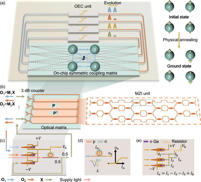
a A four-spin coupled optical Ising machine, consisting of four on-chip OEC nonlinear units and a 4 × 4 on-chip symmetric coupling matrix. Once the coupling matrix is deployed, the nonlinear coupled oscillators evolve from an initial state to the ground state of the Ising problem. b On-chip symmetric coupling matrix, comprising an optical matrix connected end-to-end with 3 dB couplers. The optical matrix, highlighted in orange, is constructed using a single-drive MZI in a rectangular unitary mesh configuration. c On-chip OEC nonlinear unit, where the differential photocurrent drives the forward-biased MRM. d The nonlinearity of the output optical power as a function of the photocurrent. e Diagram of the electric current flow in the differential photodetectors.
Figure 1b illustrates the details of the on-chip symmetric coupling matrix, which can be considered as multiple coupled Sagnac interferometers. In this system, input light is split into forward and backward paths within an optical mesh, where the light converges after completing a round-trip. Due to the reciprocity of optical linear systems, the forward and backward transmission matrices of the optical mesh are mutually transposed28. We can derive the output optical fields from Ports 1 and Ports 2 as:

where P and PT are the forward and backward complex amplitude transmission matrices of the MZI mesh, respectively, and X is the complex amplitude of the input optical vector. If the incident optical signals are mutually incoherent (e.g., operating at different wavelengths), the output light intensity will be the linear superposition of the input light intensities, and the intensity transmission matrix can be written as ref. 25:

where |A|2 denotes a matrix formed by the modulus squared of each element of matrix A. It is evident that both M1 and M2 are positive symmetric matrices. To construct a real-valued symmetric matrix, we can express the coupling matrix as:

Thanks to the inherent symmetry of the proposed optical matrix, its configurational accuracy and robustness to perturbations are superior to conventional one-way optical meshes. The optical matrix (highlighted in orange) in our design is based on an (N + 1) × (N + 1) rectangular unitary MZI mesh with a single phase shifter in each MZI (right side of Fig. 1b; see Supplementary Information S1 for derivations)25,29. The first N out of the N + 1 ports of the MZI mesh are designated as the input and output ports of the coherent optical matrix. The total number of phase shifters is N(N + 1)/2, which satisfies the minimum degree of freedom required to achieve an N × N real-valued symmetric matrix. The reduced number of phase shifters significantly lowers the energy consumption needed for configuring and maintaining the optical matrix.
Figure 1c illustrates the detailed structure of the on-chip optical-electrical coupled (OEC) nonlinear unit. Optical signals from the on-chip coupling matrix enter the germanium/silicon photodetectors, which are arranged in a differential configuration (I1-I2). The identity matrix in Eq. (6) is realized by splitting 50% of the OEC nonlinear output into another differential signal (I3). The total differential photocurrent (I1-I2-I3) directly drives the MRM, producing the corresponding nonlinear response. The intensity of the supply light determines the strength of the feedback (α). Figure 1d shows the working principle of the nonlinear transfer function. When the injected current In > 0, the MRM is forward-biased, and the transmission spectrum experiences a significant blue shift with increasing In. Conversely, when In < 0, the MRM is reverse-biased, and the spectrum shifts slightly to the red due to the much lower carrier-depleted modulation efficiency30. The nonlinear response is akin to a linearized sigmoid function. Although this function is not commonly used in optical Ising machines, we theoretically prove that it can effectively approximate the Ising problem-solving process (see Methods and Supplementary Information S2 for the capabilities of the general OEC nonlinear transfer function). In this case, the normalized output optical intensity of the OEC unit indicates the state of the corresponding spin, with a value of 1 representing ‘spin-up’ and 0 representing ‘spin-down’. Figure 1e depicts the electric current flow within the OEC nonlinear unit, where a bias current Ib provides a horizontal shift of the nonlinear transfer function.
Numerical evaluation of the proposed optical Ising machine
To highlight the advantages of the proposed optical symmetric matrix architecture, we perform a comparison of the matrix fidelity for the two structures shown in Fig. 2a. The optical MZI mesh on the right side of Fig. 1b is selected as the reference optical matrix highlighted in orange for both cases. The positive and real-valued transmission matrices are calculated using direct detection and differential detection, respectively25. For 1000 randomly generated positive and real-valued symmetric matrices, we optimize the phase shifters to maximize the correlation between the current physical matrix and the target matrix (see “Methods”). Figure 2a presents a histogram of the optimized correlations. The mean correlation of the proposed optical mesh exceeds 0.9999 for both positive and real-valued symmetric matrices, while the conventional one-way optical mesh exhibits significantly lower fidelity. The imperfect fidelity of the proposed optical mesh is partly due to the non-universality of the mesh and the local convergence of the optimization algorithm. In this simulation, all MZIs and phase shifters are ideal with high tuning accuracy. However, considering the finite programming accuracy and system noise, the experimental results show slightly worse fidelity than the simulation. We further validate the performance of the OECO Ising machine with 100 spins and a linearized sigmoid function as an approximate nonlinearity. First, we set β = 0, α = 1.1, and τ = 0.1 to verify its bifurcation capability. As shown in Fig. 2b, the 100 spins evolve from their random initial states to either ‘spin-up’ (1) or ‘spin-down’ (0) states, satisfying the first basic condition of the Ising machine. For an initial intensity Iinit > 0.5, the spin evolves to ‘spin-up’; otherwise, it evolves to ‘spin-down’. Next, we examine the performance of the OECO Ising machine in solving a 100-spin Ising problem for a random graph g05100.5, included in the Biq Mac Library, whose ground energy is known to be -39731 (see Supplementary Information S3 for tests on other graphs). Figure 2c shows the evolution of Ising energy and spin intensity when α = 0.23 and β = 0.21. After 400 roundtrips, the Ising energy reaches the ground state and stabilizes. It is noted that the spin intensity will not always evolve to exactly 0 or 1 in a physical Ising machine. Therefore, a threshold of 0.5 is used to determine the final state of the spin. Finally, we investigate the influence of α and β on the success rate of the Ising machine. The sweeping step for both parameters is 0.01, and the success rate is counted for 100 random initial states. Figure 2d shows the sweeping results, where the maximum success rate exceeds 0.2. Compared to other nonlinearities, the success rate of our model is nearly half, which is attributed to higher amplitude inhomogeneity. This can be suppressed through engineering of the nonlinear response27 (see Supplementary Information S4 for the influence of noise).
Fig. 2: Numerical investigation of the proposed optical Ising machine.

a Comparison between the proposed paradigm and the conventional approach for constructing the symmetric matrix through numerical simulations. The optical matrix, highlighted in orange, is the same in both setups and is shown on the right side of Fig. 1b. The final correlation of 1,000 random symmetric matrices is tested and analyzed in the histogram. b Evolution of the proposed OECO system above the bifurcation point (α = 1.1), where the system evolves into either the ‘spin-up’ (1) or ‘spin-down’ (0) state. The parameter Iinit represents the initial intensity of the spin. c Evolution of Ising energy and spin amplitude for α = 0.23 and β = 0.21. The test graph is g05100.5 from the Biq Mac Library. d Success rate of g05100.5 under a sweep of α and β.
Experiment investigation of the proposed optical Ising machine
The OECO Ising machine chip is fabricated in the standard silicon photonics foundry, with a silicon layer of 220 nm in thickness. A microscope image of the chip is shown in Fig. 3a. The germanium/silicon photodetector and MRM are adopted from the process design kits, and they exhibit typical 3 dB bandwidths exceeding 40 GHz and 50 GHz (in carrier-depleted mode), respectively. Figure 3b shows the packaged chip with optical fiber array and electrical wire-bonding. Due to the forward-biased operating mode of the MRM, along with low-frequency packaging and power supply limitations, the actual operating bandwidth of the OEC unit is approximately 100 MHz, resulting in a corresponding latency of 1.6 ns (see Supplementary Information S5). The optical feedback length is approximately 8 mm, corresponding to a time constant of τ ≈ 0.11 ns, which is much shorter than the latency determined by the system’s bandwidth. However, it has been shown that both latencies can be considered together as a single effective latency without compromising system functionality (see Supplementary Information S6). Figure 3c displays the measured response of the photodetector under varying bias voltages, where the linear responsivity is 0.8 A/W. Figure 3d provides a close-up photograph of the OEC nonlinear unit, where the bias voltage V is set to 3 V to ensure the photodetector operates in the linear region. Figure 3e shows the transmission spectrum of the differentially driven MRM, excited by incremental differential optical power. The transmission spectrum for zero input is highlighted separately, and the corresponding nonlinear transfer function at the zero-input resonant wavelength is measured, as shown in Fig. 3f, which aligns well with our theoretical predictions. The optical power required to excite the spin state from 0 to 1 is less than 1 mW, indicating that the on-chip OEC unit is more energy-efficient compared to other nonlinearities used in previous Ising machines.
Fig. 3: Chip fabrication and basic characterization.
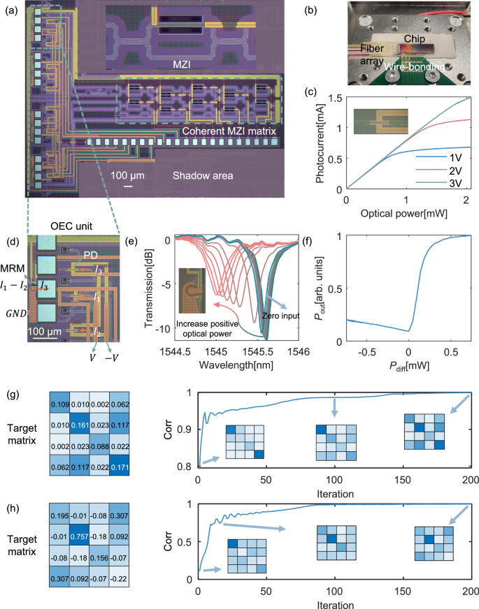
a Microscopic photograph of the optical Ising machine. b Photograph of the packaged optical Ising machine chip. c Photocurrent of the on-chip photodetector under different bias voltages. d Zoom-in photograph of the OEC unit. e Drift of the transmission spectrum of the MRM with increasing differential optical power. f Measured nonlinear transfer function of the OEC unit. Pdiff denotes the differential input power, and Pout denotes the output power. g Evolution of matrix correlation given a random target positive-valued symmetric matrix. h Evolution of matrix correlation given a random target real-valued symmetric matrix.
The fidelity of the on-chip symmetric matrix is experimentally evaluated in the next step. We randomly select one positive and one real-valued symmetric matrix as targets and configure the on-chip optical mesh using a gradient descent algorithm (see “Methods”). The iteration curves for correlation are shown in Figs. 3g and h. The final optimized correlations are 0.9992 and 0.9979 for the two cases, respectively, while the mean correlations for positive and real-valued symmetric matrices are 0.998 and 0.986, as detailed in Supplementary Information S7. These results demonstrate that the proposed symmetric optical matrix can effectively represent the necessary symmetric matrix in the optical Ising machine.
The nonlinear coupled oscillators start with all spins in the ‘spin-down’ state. Therefore, it cannot automatically evolve to the ground state without additional excitations to provide an appropriate initial state. To emulate an arbitrary initial state, four independent channels of excitation signals would be necessary. In the subsequent experiment, only one excitation optical pulse is injected into the positive channel of the first OEC nonlinear unit, as shown in Fig. 4a. The excitation can also be integrated on-chip to facilitate testing of arbitrary initial states. In our setup, the supply light intensity is set to 4 dBm, while the maximum intensity of the excitation light is -6 dBm. The excitation pulse intensity determines the initial spin state. After the excitation pulse is withdrawn, the system begins its evolution towards the ground state from the corresponding initial state.
Fig. 4: Experimental verification of bifurcation in the proposed optical Ising machine.
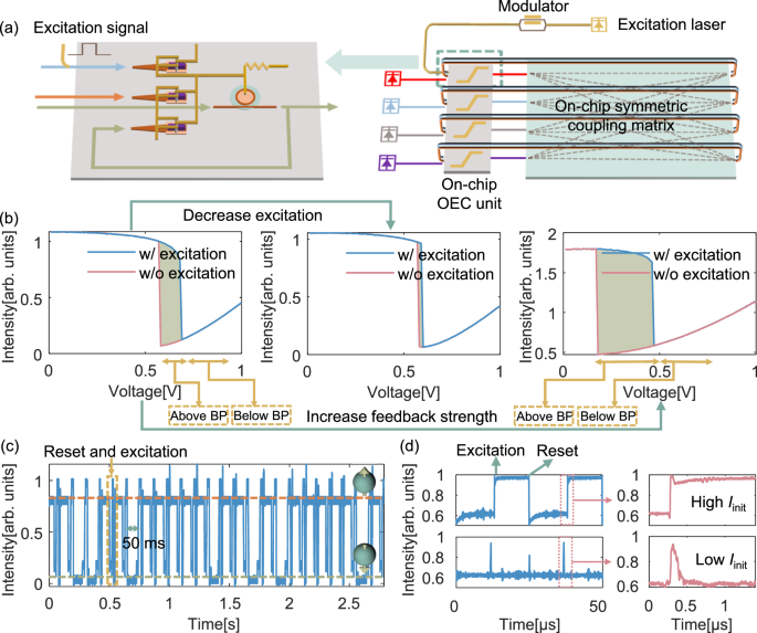
a Experimental setup of the optical Ising machine, where the initial states of all spins are ‘spin-down’. A positive excitation pulse is sent to one of the OEC units, triggering the physical evolution of the optical Ising machine. b Influence of the nonlinear function (voltage applied to the thermal phase shifter of MRM), feedback strength (intensity of supply light), and initial state (intensity of excitation pulse) on the oscillation of the nonlinear cavity. The olive zones represent the working voltages where the cavity can oscillate under the current initial state and feedback strength. BP denotes the bifurcation point. c Bifurcation of the nonlinear oscillator under random excitation signal intensity. d Time response of the oscillator with a 40 kHz excitation signal and a 0.1% duty cycle. The upper and lower waveforms correspond to strong and weak excitation, respectively.
To start, we train the on-chip MZI mesh to act as an identity matrix to examine the bifurcation of a single OECO, with only the supply light of the first OEC nonlinear unit turned on. The control parameter for bifurcation is the self-feedback strength α, which corresponds to the power of the supply light. Above the bifurcation point, the spin will evolve to either ‘spin-up’ or ‘spin-down’, determined by the initial state. Below the bifurcation point, the spin remains in a fixed point regardless of the initial state. In addition, the bifurcation point is also influenced by the voltage applied to the thermal phase shifter of MRM, which controls the horizontal shift of the nonlinear function (see Eq. (8) in Methods).
We modify the working point of the MRM by sweeping the voltage, as shown in Fig. 4b. The sweeping curve shows an abrupt drop followed by a slow rise, attributed to the thermal effect within the ring. This occurs at high supply light power to generate a sufficient gain coefficient (α). The working region with lower voltage is above the bifurcation point, while the region with higher voltage falls below it. When an excitation pulse is applied, the MRM, which operates in the shadow region (0.58 V to 0.69 V), evolves to ‘spin-up’. As the intensity of the excitation pulse decreases, the working region (0.6 V to 0.69 V) eventually evolves to ‘spin-down’, consistent with the simulation results in Fig. 2b. Increasing the intensity of the supply light widens the working region above the bifurcation point.
Next, we select a suitable operating point for the MRM (0.63 V) to balance the probabilities of the binary states during bifurcation. We then input a sequence of excitation signals with random intensities to observe the bifurcation process. It is important to note that once the spin evolves into the ‘spin-up’ state, subsequent positive excitation pulses maintain the oscillation in the cavity, resulting in no change to the spin output intensity, regardless of the excitation pulse intensity. To clearly demonstrate the bifurcation, we reset the MRM to the ‘low-pass’ state before each new excitation pulse. This is achieved by applying a large voltage (0.8 V) to the thermal phase shifter and then returning it to 0.63 V. In practical Ising problem-solving, the reset operation is not restricted to the method described above and can be adapted based on the need for repeated testing. Figure 4c shows the captured waveform of the OEC output signal, where the time span between the adjacent excitation and reset pulses is about 50 ms. This long interval is chosen to allow for the observation of the binary states as the spin intensity stabilizes. The spikes in the waveform are attributed to the excitation and reset pulses. The deterministic evolution towards either ‘spin-up’ or ‘spin-down’ meets the basic requirements of the Ising machine.
To measure the characteristic time of spin evolution, we use excitation and reset pulses with a frequency of 40 kHz, a duty cycle of 0.1% (corresponding to a 25 ns pulse width), and rise-fall times of 48.8 ns. Figure 4d shows the OEC output signal waveforms for strong (upper panel) and weak (lower panel) excitation pulses, respectively. Upon withdrawal of the excitation pulse, the spins in the upper and lower panels evolve to the ‘spin-up’ and ‘spin-down’ states, respectively. These two cases correspond to the high and low initial intensity (Iinit) scenarios from the simulation in Fig. 2b. The evolution time is approximately 150 ns, indicating that the spins take only a few round trips to reach the steady state. The waveforms of the excitation and reset pulses are provided in Supplementary Information S8.
Finally, we solve a benchmark Ising problem with four coupled spins using the optical Ising machine chip. As shown in Fig. 5a, Spins 1 and 3 are positively correlated, as are Spins 2 and 4, while Spins 2 and 3 are negatively correlated. Using the coupling matrix in Fig. 5a and selecting α = 0 (i.e., setting the diagonal elements of the on-chip matrix to zero), we train the on-chip symmetric matrix, as depicted in Fig. 5b. The excitation signal here is injected into the second channel of spins to demonstrate the versatility of our chip. The excitation intensity is kept consistent with that of previous experiments, ensuring that the final state of the second spin is 1. Under this excitation, the system evolves to the ground state of the Ising problem, which is known to be [-1 1 -1 1]. As in the previous setup, excitation and reset signals are alternately applied to the system with a time span of 10 ms. Figure 5c shows the evolution of the four OEC nonlinear units. The four spins successfully evolve to the ground state through physical annealing. In Fig. 5d, the evolutions of the four spins over time are shown together. Spins that end up in the same state have different final intensity values, partially due to the amplitude inhomogeneity of the Ising machine and slight differences in the power of the supply light. In addition, some of the observed waveform oscillations may be attributed to microwave oscillations occurring within the OECO feedback loop. The four reset and one excitation signals are supplied by low-speed electrical sources due to our limited channel of high-speed signals. Therefore, the evolution time of several microseconds is partly limited by the establishing time of the excitation signal (see Supplementary Information S8). To further demonstrate the versatility of the fabricated Ising machine chip, we solve two additional non-trivial Ising problems on-chip (see Supplementary Information S9). The results confirm that the proposed optical Ising machine is well-suited for solving a variety of Ising problems (The success rate is tested in Supplementary Information S10).
Fig. 5: Experiment demonstration of four-spin Ising problem solving.
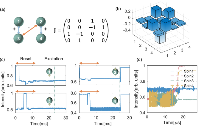
a The Ising problem with its corresponding coupling matrix. b The actual coupling matrix deployed on the optical matrix. c Evolution of the four spin states under a specific excitation. d Zoomed-in view of the evolution process of the four spins.
Discussion
Scalability of the optical Ising machine
The on-chip optical symmetric matrix can be constructed using a two-layer waveguide structure, as illustrated in Fig. 1b. The MZI mesh is positioned in the lower layer, while the end-to-end connecting waveguides are placed in the upper layer. To avoid wavelength-dependent interference and delay misalignment within the mesh, it is crucial that the length of each path in the symmetric optical matrix be identical. This two-layer architecture enhances layout efficiency, making the design more space-efficient and convenient. This approach is already supported by most standard silicon photonic foundries, such as those with one layer of silicon and one layer of silicon nitride32. The MZI mesh has already been scaled up to 64 × 6433, with the size of a single MZI being 357 μm × 90 μm in our fabricated chip. The total footprint of a 4 × 4 MZI mesh is 0.64 mm², and for a 64 × 64 MZI mesh, it is 133.66 mm²—both of which are still smaller than bulky devices like lenses and spatial light modulators. This demonstrates the scalability potential of the proposed optical symmetric matrix architecture. Moreover, the optical coupling matrix can be optimized to achieve a training-free configuration during Ising problem solving (see Supplementary Information S11). For the OEC nonlinear unit, the footprint of the photodetector and MRM are just 10 μm × 110 μm and 30 μm × 45 μm, respectively. Considering the electrical interconnection, the total footprint of the OEC nonlinear unit is comparable to that of a single MZI unit, which is approximately 0.01 mm². Therefore, the OEC nonlinear units contribute only slightly to the overall footprint of the optical Ising machine (5.9% for four spins and 0.5% for 64 spins).
Energy efficiency and converge speed of the optical Ising machine
By integrating both optical linear and nonlinear computations onto a single chip, the need for AD/DA conversion is eliminated, reducing energy consumption. As a result, the primary sources of energy consumption in the optical Ising machine chip are the laser source and the electric power supply of the nonlinear unit. While the energy required to maintain the optical matrix is significant and scales with N2, it is expected to be eliminated in the future through the use of advanced nonvolatile phase shifters34. The excitation pulse is active only during the initiation of the Ising machine’s operation, so its power consumption is also negligible. Considering that a differential optical power of 0.5 mW is sufficient to alter the spin state, the total optical power for a single spin can be reasonably estimated as 1 mW. Given the average photocurrent of 0.5 mA (for I1 and I2 + I3) and a bias voltage of 3 V, the electrical power consumption of each OEC nonlinear unit is 3 mW. Therefore, the total power consumption of the proposed optical Ising machine chip can be estimated as 4 N mW, where N represents the number of spins. With further optimization, the state-of-the-art OEC unit could reduce its power consumption to as low as 0.15 mW35. The convergence speed of our proposed system is primarily determined by the RC bandwidth of the OEC nonlinear unit, as the on-chip delay for matrix multiplication is negligible. In contrast, other optical Ising machines that employ electrical matrix multiplication or electrical algorithm annealing are mainly limited by factors such as fiber loop length, AD/DA conversion, and the time required for electronic computation. With appropriate engineering of the parasitic capacitance and bias circuit, the RC bandwidth of the OEC unit can exceed 1 GHz35. With these enhancements, the convergence time can be reduced to r × 0.1 ns, where r denotes the number of roundtrips, which depends on the specific Ising problem and system parameters. Table 1 compares different implementations of optical Ising machines in terms of nonlinearity footprint, energy efficiency, and convergence speed. Our proposed scheme outperforms existing architectures in terms of footprint and energy efficiency, offering a promising pathway toward large-scale, monolithically integrated optical Ising problem solvers.
Table 1 Comparison of different implementations of optical Ising machine

In conclusion, we present a monolithically integrated OECO system for optical Ising machines, offering enhanced efficiency and scalability. The optical coupling matrix is optimized to minimize the number of phase shifters while maintaining high accuracy in realizing real-valued symmetric matrices. The compact footprint and low driving power of the OEC nonlinear unit enable the potential for large-scale, monolithically integrated optical Ising machines. Both numerical simulations and experimental validation confirm the fidelity of the optical symmetric matrix and the effectiveness of the Ising solver. In addition, we demonstrate the successful solution of various four-spin Ising problems. Our approach provides significant advantages in integration density, energy efficiency, and scalability, laying a strong foundation for the development of chip-scale optical recurrent nonlinear accelerators.
Methods
The principle of on-chip OECO-based Ising machine
First, it is essential to demonstrate the equivalence of two nonlinear transfer functions with relative vertical translation and scaling in the Ising machine model. A simple nonlinear transfer function (Supplementary Fig. S14a) and the discrete form of the evolution of the coupled oscillators system that employs it can be written as:

When the nonlinear function undergoes a vertical scaling by a factor of ρ and a vertical translation by ρd, Eq. (7) becomes equivalent to horizontally translating the new function by ?∑?=1???,? (Supplementary Fig. S14b) and implementing the following transformation:

Therefore, we only need to prove the competence of the simple nonlinear function now. Next, the Lyapunov function, defined as the negative of the summed primitive function with respect to xi, for the right-hand side of Eq. (2) is expressed as ref. 27:

Assuming that the final amplitude of the spin is either d or -d, and that τ is much smaller than xi, the Lyapunov function can be expressed as:

In the final stable state, the right-hand side of Eq. (2) is zero. Therefore, the stable state of the system corresponds to the extremum of L, which represents the Ising energy. Furthermore, setting the right-hand side of Eq. (2) to zero leads to the following relation:

Summing the inequalities with respect to xi, we can derive the following:

Therefore, if α-1 lies between the minimum and second minimum of −??∑?,?=1???,?σ?σ?, the stable state of the system corresponds to the ground energy of the Ising problem.
Numerical methods
In the simulation and experiment, we use the gradient descent algorithm to configure the symmetric matrix. Given a target matrix T and the measured real-time matrix M, the cost function is defined as the correlation between them:

where T1:4,i and Ti,1:4 represent the i-th column and row of matrix T, respectively. The goal is to maximize the correlation by optimizing the voltages applied to the thermal phase shifters. The detailed process of the gradient descent algorithm is outlined as follows.
- (A)Randomly initialize the voltages applied to the thermal phase shifters;
- (B)Increase the voltage by 0.05 V for each thermal phase shifter and calculate the cost function corr(U + 0.05) respectively;
- (C)Decrease the voltage by 0.05 V for each thermal phase shifter and calculate the cost function corr(U-0.05) respectively;
- (D)Estimate the approximate gradient of the cost function by

- (E)Update the voltages using the Adam algorithm, a fast-converging gradient descent method36:

where iter is the current iteration, α is the learning rate (set to 0.1 during training), and β1, β2, and ε are set to 0.9, 0.999, and 10–8, respectively. The initial values of viter and siter are zero.
- (F)Repeat steps (B-E) until the cost function converges and save the optimized voltages.
Experiment methods
The chip is fabricated at the Chongqing United Microelectronics Center (CUMEC) using its 200 mm CMOS process line, which includes two-layer copper interconnects. The on-chip photodetector employs a lateral PIN structure with a germanium layer that is 260 nm thick. In the matrix configuration experiment, the wavelengths of 1545.8 nm, 1546.4 nm, 1547 nm, and 1547.6 nm are selected as the working wavelengths for the four input ports. To measure the precise on-chip symmetric matrix, only one of the four laser sources is activated at a time, with each source being calibrated to have the same intensity. As a result, the chip output of each laser source corresponds to one column of the symmetric matrix. The excitation laser source at 1547.6 nm is modulated by a lithium niobate intensity modulator with a 10 GHz bandwidth. The wavelength of the excitation light can be arbitrarily chosen within the C-band. Excitation and reset pulses are generated using an arbitrary waveform generator (RIGOL DG4202), and the output optical signals are detected by a photodetector with a 200 MHz bandwidth. The electric signals are captured by an oscilloscope (RIGOL DS4022). The voltages applied to the thermal phase shifters, as well as the bias voltage for the OEC nonlinear unit, are provided by a digital-to-analog converter (LTC2688) and controlled by a field-programmable gate array (FPGA) chip (7K325T). The entire experimental system is managed by a personal computer via serial ports. The chip is thermally stabilized using a thermoelectric cooler (TEC).