


The challenges of fabricating low-loss waveguides and the reliance on bulky external magnets hinder the miniaturization of Faraday isolators. Now, researchers have overcome this limitation by femtosecond laser writing of waveguides within latched garnet.
Reciprocity is a topic of great importance in both optical theory and practice. In typical optical systems, the transmission of light adheres to the Lorentz reciprocity principle, which states that when the positions of the light source and detector are swapped, the detection result remains unchanged. When considering the temporal evolution of the system, we observe that a reciprocal system is symmetric under time reversal, provided the material's dissipative properties and external bias field remain constant1. This symmetry arises because the Maxwell equations governing the electromagnetic field are invariant under time reversal, with only the direction of propagation changing, while other properties remain unaffected. Consequently, time-reversal symmetry is equivalent to reciprocity. Even in complex optical systems, in the absence of nonlinear effects, magneto-optical effects, chiral material or time-dependent changes in optical properties, reciprocity still holds.
Overcoming the limitations of the reciprocity principle to enable non-reciprocal light transmission holds great potential for both practical applications in functional optical devices and for advancing fundamental research. Key components in optical systems, such as isolators and circulators, are representative examples of non-reciprocal devices. Isolators are typically placed immediately after the laser, enabling the emitted light to pass smoothly while blocking reflected light from reverse transmission, thereby protecting the laser from the detrimental effects of stray reflections. Theoretical investigations into non-reciprocity have also opened new research avenues in quantum optics and condensed matter physics, including chiral atom–light coupling2, optical topological non-reciprocal lasers3, non-reciprocal phase transitions4, and non-reciprocal Hall effects5.
Non-reciprocity is typically achieved through the Faraday effect in magneto-optical materials. By applying a bias magnetic field to the magneto-optical material, the optical device exhibits a non-reciprocal response due to the antisymmetric nature of the magnetic field under time-reversal. This principle is employed in the construction of isolators used in commercial lasers. However, integrating magneto-optical materials for non-reciprocity presents significant challenges in device integration. The absence of integrated non-reciprocal devices will lead to serious issues, such as laser backscatter and signal crosstalk in integrated photonic chips, thereby limiting the information processing capabilities of future large-scale photonic chips. Consequently, realizing integrated broadband non-reciprocal devices is crucial. Currently, efforts are being made both to explore magneto-optical integrated chips and to develop new magnetic-free non-reciprocal principles and devices.
Magnetic-free optical isolators typically employ active spatio-temporal modulation to achieve non-reciprocity6,7,8, such as acousto-optic modulation, electro-optic modulation, and cavity optomechanical interactions. However, since they often rely on cavity structures to enhance modulation strength while minimizing power consumption, they are limited in terms of operating bandwidth by the resonance linewidth. On the other hand, magneto-optical non-reciprocity, owing to its significant success in traditional optical isolators, has naturally become one of the most promising solutions for integrated non-reciprocal technology. The challenges it faces include the low magneto-optical coefficients of standard optoelectronic materials, difficulties in growing and processing magnetic materials with low loss (which complicates integration into photonic chips), and the requirement for a certain degree of external magnetic field9.
Now, writing in Nature Photonics, Jerome Lapointe and co-workers successfully demonstrate an approach that allows one to make submillimetre-sized passive optical isolators without external magnets, holding promise for hybrid integration into photonic chips10. The isolators combine insertion loss below 1.5 dB and isolation ratio in excess of 25 dB. They are capable of operating across a wide range of optical input power levels and offer an operating bandwidth of 90 nm.
Given the limitations of traditional materials, which exhibit low magneto-optical coefficients and require external magnetic fields, the authors have utilized a latched ferromagnetic bismuth-doped iron garnet (BIG) with an optimized composition. This material, which became commercially available in recent years, exhibits a strong Faraday rotation (magneto-optical effect) of –93°/mm at 1,550 nm under magnetic poling with a strong external magnetic field. It retains this effect even after the magnetic field is removed, eliminating the need for external magnets — a key feature for miniaturization. To address the challenges of on-chip integration, Lapointe and co-workers have developed a novel fs-laser writing approach to fabricate low-loss Faraday rotator waveguides within BIG slabs. Since BIG undergoes a negative index change upon femtosecond pulse irradiation, the approach of modifying only the waveguide cladding was naturally employed to inscribe the waveguides, which feature a smooth, homogeneous, cylindrical structure.
Figure 1a illustrates the alternating spiral-helix laser writing technique. A complete waveguide, regardless of its cladding thickness, can be inscribed in a single scan at a constant speed by utilizing (i) a spiral to fill the bottom horizontal layer, (ii) a helix to ascend vertically, alternating inward and (iii, iv) outward within the cladding plane. The red lines in Fig. 1a represent the newly inscribed laser tracks. Furthermore, starting and ending the laser writing scan on the outer surface of the cladding (at (i) and (iv), respectively) ensures that no non-uniformity forms at the interface between the waveguide core and the cladding10. As a result, waveguides with an insertion loss of less than 0.15 dB can be produced while maintaining full magneto-optic functionality. Although the high stress generated during dicing the slabs may compromise the remanent magnetization of the waveguide, the BIG slabs can be re-poled and regain their full performance by applying a uniform magnetic field of >4000 Oe. Assembling BIG Faraday rotator waveguide slabs between two polarizers offset by 45° creates optical isolators. Lapointe and co-workers placed a BIG Faraday waveguide between two 30-µm-thick Polarcor UltraThin polarizers, butt-coupled to two 1,550-nm standard fibres secured with optical adhesive. The final isolator exhibits total insertion losses of less than 1.5 dB and an isolation ratio exceeding 25 dB across the optical telecommunication C-band.
Fig. 1: Magnetless Faraday rotator waveguide fabrication and integration.
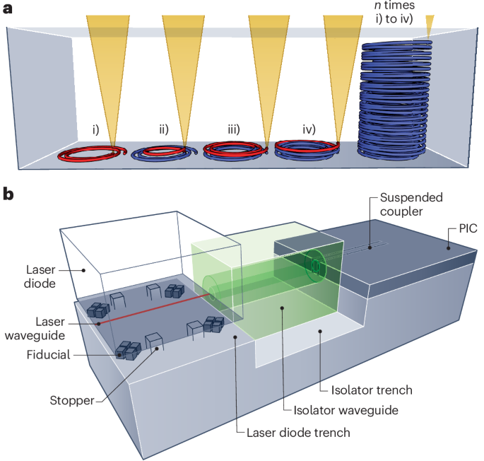
a, Illustration of the alternating spiral-helix laser writing technique for the fabrication of a magnetless Faraday rotator waveguide. b, Schematic illustration of laser-isolator–PlC hybrid integration. Figure adapted with permission from ref. 10, Springer Nature Ltd.
For their initial singulated prototypes, the 480-µm-thick BIG slab was first saw-blade diced to a size of 400 µm x 400 µm. The 30-µm-thick Polarcor plates were then laser-welded to the BIG slab and laser-cut around the sample using the same laser system employed for the waveguide inscription. Considering the isolator’s spatial dimensions of 50 µm x 50 µm x 540 µm and the current packaging technologies used for integrating laser sources or photodetectors, the isolator shows great potential for laser-isolator–PIC hybrid integration, as illustrated in Fig. 1b.
The work by Lapointe and co-workers demonstrates a magnetic waveguide isolator via fs-laser writing. By utilizing the same technology and approach, it is possible to inscribe waveguides of various sizes tailored to match the mode field diameters and wavelengths of different photonic components, such as lasers, enabling direct integration into the optical path without the need for intermediate elements. Furthermore, the increasing adoption of photonic wire bonding for optical interconnections offers an additional method for incorporating these isolators into a wide range of photonic chips, regardless of the presence of deep-etch cavities. Although challenges remain to fully realize the newly proposed hybrid integrated configuration, industry-worthy integrated optical isolators are becoming increasingly attainable.