Organic–inorganic hybrid perovskite solar cells (PSCs) have shown impressive photoelectric conversion efficiency (PCE) but suffer from inevitable degradation when exposed to air and light. Replacing the organic cations with inorganic Cs+ to yield all-inorganic CsPbX3 perovskites can improve the stability under environmental pressure. Among them, cesium lead bromide (CsPbBr3) perovskite shows great environmental tolerance under illumination, humidity, heat, and oxygen attack. However, the energy gap between the carbon electrode and CsPbBr3 limits the carrier separation–transfer rate. Herein, p-type charge-transfer-doped NiO nanocrystals are employed as hole transport materials in all-inorganic CsPbBr3 PSCs with a fluorine-doped tin oxide (FTO)/SnO2/CsPbBr3/NiO-l-Cys/carbon structure. This combination reduces the charge-carrier recombination by decreasing the hole transport potential energy-level barrier between the perovskite and the hole transport layer. The coordination of the energy structure associated with the interfacial charge extraction–transfer action leads to a remarkable enhancement in PCE (9.61%) and a much higher open-circuit voltage (1.614 V), surpassing those achieved by hole-free devices (7.35% and 1.504 V, respectively). The PSC device assembled with NiO nanocrystals displays good stability under high humidity and temperature for 30 days. The greatly improved PCE, coupled with good stability, demonstrates the great potential of l-cysteine-doped NiO for future use as a hole-transporting material in all-inorganic PSCs.
Introduction
Click to copy section linkSection link copied!
Perovskite solar cells (PSCs) exhibit great efficiency, low cost, and easy solution processing, demonstrating great potential as next-generation photovoltaics for future energy supply. The photoelectric conversion efficiency (PCE) of organic–inorganic hybrid PSCs has rapidly increased from 3.8 to 26.1% in just a few years due to optimization of the light absorption layer, continuous exploration, and innovation in materials for the hole transport and electron transport layers (ETL) in PSC devices. This achievement brings them closer to the theoretical value and places them on par with leading silicon solar cells. (1−5) Unfortunately, hybrid perovskites still suffer from inevitable degradation under air and light induced by the destruction of high polar covalent bonding between the monovalent organic cation and octahedral PbI2. (6−8) Replacing organic cations in the organic–inorganic hybrid PSCs with inorganic Cs+ to generate all-inorganic CsPbX3 perovskites may improve the stability under environmental pressure. (9−12) Among all-inorganic CsPbX3 perovskites, CsPbI3 possesses a proper bandgap of 1.73 eV, achieving a high efficiency of approximately 21.75%. (13) However, despite the optimum bandgap, black phase CsPbI3 still suffers from an imperfect tolerant element triggering a metastable stage steadiness, leading to quick and easy degradation to a nonphotoactive yellow stage with an extensive bandgap of 2.82 eV under an ambient environment. (14)
By comparison, tribrominated cesium lead bromide (CsPbBr3) perovskite shows great environmental tolerance under illumination, humidity, heat, and oxygen attack, making it potentially suitable for use in photoelectric devices, communication systems, electrical power plants, satellites, spacecrafts, space-based solar power plants, and so on. (15−17) Nevertheless, fewer CsPbBr3 PSCs have been reported so far when compared to organic–inorganic hybrid PSCs due to their big optical bandgap that results in reduced spectral absorption, leading to the recombination loss at interfaces and grain boundaries owing to the energetic mismatch. (18) To solve these issues, tremendous efforts have been devoted to improving the intermediate energy levels for filling the bandgap and accelerating the charge-carrier extraction for better photoelectric performance, including optimization of the structure of the electron transport layer and the hole transport layer. (19,20) Spiro-OMeTAD is a common hole transport material used in perovskite solar cells. However, its small organic structure, complex synthesis process, poor long-term environmental stability, and relatively high cost seriously restrict their commercial use in the future. (21) In this view, nickel oxide (NiO) has attracted considerable attention for use in the hole transport layer owing to its several advantages: (22−25) First, the highest occupied orbital of NiO is higher than that of perovskite, which shows excellent energy-level alignment with hole transport materials and perovskite, enhancing the extraction ability of the holes in the perovskite. Second, NiO demonstrates excellent chemical stability in the air environment due to its inorganic oxide nature, ensuring the stable performance of the battery. Third, an ideal hole mobility and block electrons reduce the loss of holes and avoid carrier recombination. Four, the materials are easy to prepare and have a low cost. However, NiOx-based PSCs still suffer from several problems. For example, the mismatched interfacial energy level at NiOx and the perovskite results in a big energy offset. (26) Also, NiOx films prepared at room temperature usually contain large amounts of impurities and surface defects, accumulating holes at the perovskite/NiOx interface. (27) These challenges can be addressed by introducing organic molecules between the perovskite and NiO layers to significantly improve the hole extraction and transport. (28,29) However, little work has been carried out in this field of research, opening new avenues for investigating high-efficency PSCs.
Herein, l-cysteine (l-Cys)-doped NiO nanocrystals are employed as hole transport materials in carbon-based, all-inorganic CsPbBr3 PSCs. By tuning the valence band (VB) maximum edge of NiO-l-Cys nanocrystals, the best device can achieve the champion open-circuit voltage (VOC) of 1.614 V. Moreover, the device shows nearly unchanged PCE performance after storage under environmental conditions for over 30 days, mainly due to improved hole conductivity and reduced defects in the perovskite surface.
Experimental Section
Click to copy section linkSection link copied!
Materials
The reagents methanol, ethanol, acetone, isopropyl alcohol, l-cysteine (l-Cys), lead bromide (PbBr2, ≥99.0%), and cesium bromide (CsBr, ≥99.9%) were purchased from Aladdin. N,N-Dimethylformamide (DMF), thiourea (CH4N2S, ≥99.0%), and NiO nanoparticles were provided by Macklin. Stannous chloride was obtained from Alfa Aesar, and fluorine-doped tin oxide (FTO, OPV-FT022-7) glass was received from OPV Tech Co. Ltd.
Preparation of SnO2 Quantum Dots (QDs) and NiO-l-Cys Solution
SnO2 QDs solution was prepared by the following low-temperature solution technology: 1.706 g of stannous chloride and 0.676 g of thiourea were dissolved in 60 mL of deionized water and kept under constant agitation for 36 h at room temperature to yield a yellow liquid containing SnO2 QDs. The product was centrifuged at 9000 rpm for 5 min and filtered with a poly(tetrafluoroethylene) (PTFE) membrane (0.22 μm), obtaining a brilliant yellow SnO2 QDs solution before use. Besides, 10 mg of NiO nanoparticles and 10 mg of l-cysteine were dispersed in 1 mL isopropanol by ultrasonication to obtain a NiO-l-Cys solution.
Preparation of All-Inorganic CsPbBr3 PSCs
All processes were carried out under an air atmosphere without any additional condition control. The FTO substrate was etched with a 2 M HCl solution and Zn powder, followed by washing with detergent, distilled water, acetone, isopropanol, and ethanol. To improve its wettability, the washed FTO substrates were plasma-treated under air conditions to generate hydroxyl radicals on the FTO glass surface. The FTO substrate and SnO2 QDs solution were preheated at 80 °C. Then, the SnO2 QDs solution was spin-coated on the FTO surface for 30 s at 2000 rpm and annealed in air at 200 °C for 1 h to obtain a tense SnO2 electron transport layer (ETL). Inorganic CsPbBr3 perovskite films were then deposited on the surfaces of the FTO/SnO2 substrate by spin-coating of 1 M PbBr2 DMF solution at 2000 rpm (90 °C for 30 s) and 0.07 M CsBr methanol solution at 2000 rpm for 30 s with several times. After being rinsed with isopropanol, the obtained perovskite films were dried at 250 °C for 5 min. Subsequently, NiO-l-Cys isopropanol solution was spin-coated for 30 s under 2000 rpm, followed by annealing at 250 °C for 15 min. Finally, the carbon electrode was used to cover the CsPbBr3 perovskite film surface through the doctor-blade coating approach, and a complete PSC was obtained.
Characterization
The morphologies were viewed by a field-emission scanning electron microscope (S4800, Hitachi). The crystalline structures were characterized by X-ray diffraction (XRD, Bruker D8 Advance) with Cu Kα radiation. The depth-dependent grazing incident X-ray diffraction patterns were obtained using an X-ray diffractometer (Bruker D8 Advance). Further characterizations were carried out using X-ray photoelectron spectroscopy (XPS, PHI-5000CESCA, PerkinElmer) and ultraviolet–visible (UV–vis) absorption spectrometry (Meipuda, UV-5600). Elemental composition was determined by energy-dispersive spectroscopy (EDS) (XFlash 610-M, Bruker Nano GmbH). Ultraviolet photoemission spectroscopy (UPS) tests were performed on a Kratos AXIS ULTRA system, and atomic force microscopy (AFM) was carried out on a Kelvin probe force microscope. The contact angle of the perovskite film was measured by using a contact angle analyzer (Dataphysics OCA20).
The photocurrent–voltage (J–V) curves of the solar cells were recorded by using an electrochemical workstation (CHI660E) under simulated solar light irradiation at an optical intensity of 100 mW·cm–2 (Perfectlight, CHF-XM-500W) in the voltage range 0–1.7 V. The incoming photon-to-electron conversion efficiency (IPCE) spectra were recorded by a comprehensive system (Enli Technology Co., Ltd.). The trap densities of perovskite films used in electron-only devices with the structure FTO/SnO2/CsPbBr3/NiO-l-Cys(or NiO)/carbon at voltages of 0–7 V were characterized by a space-charge-limited current (SCLC) model under dark conditions. The capacitance–voltage (C–V) curve was detected at a frequency of 5 kHz (amplitude of 30 mV) under dark conditions. Stable-state photoluminescence (PL) and time-resolved photoluminescence (TRPL) spectra were collected by FLS920 and Horiba spectrofluorometers under the excitation wavelengths of 385 and 510 nm. The dark J–V curves of devices were obtained at a scanning rate of 10 mV·s–1 in the voltage range of −1.5 to 1.5 V. Electrochemical impedance spectroscopy (EIS) was performed in the dark under a frequency from 1 MHz to 0.1 Hz with an amplitude of 10 mV at VOC. Steady-power output curves were recorded at the maximum power point (MPP) at the bias voltage of the maximal power output.
Results and Discussion
Click to copy section linkSection link copied!
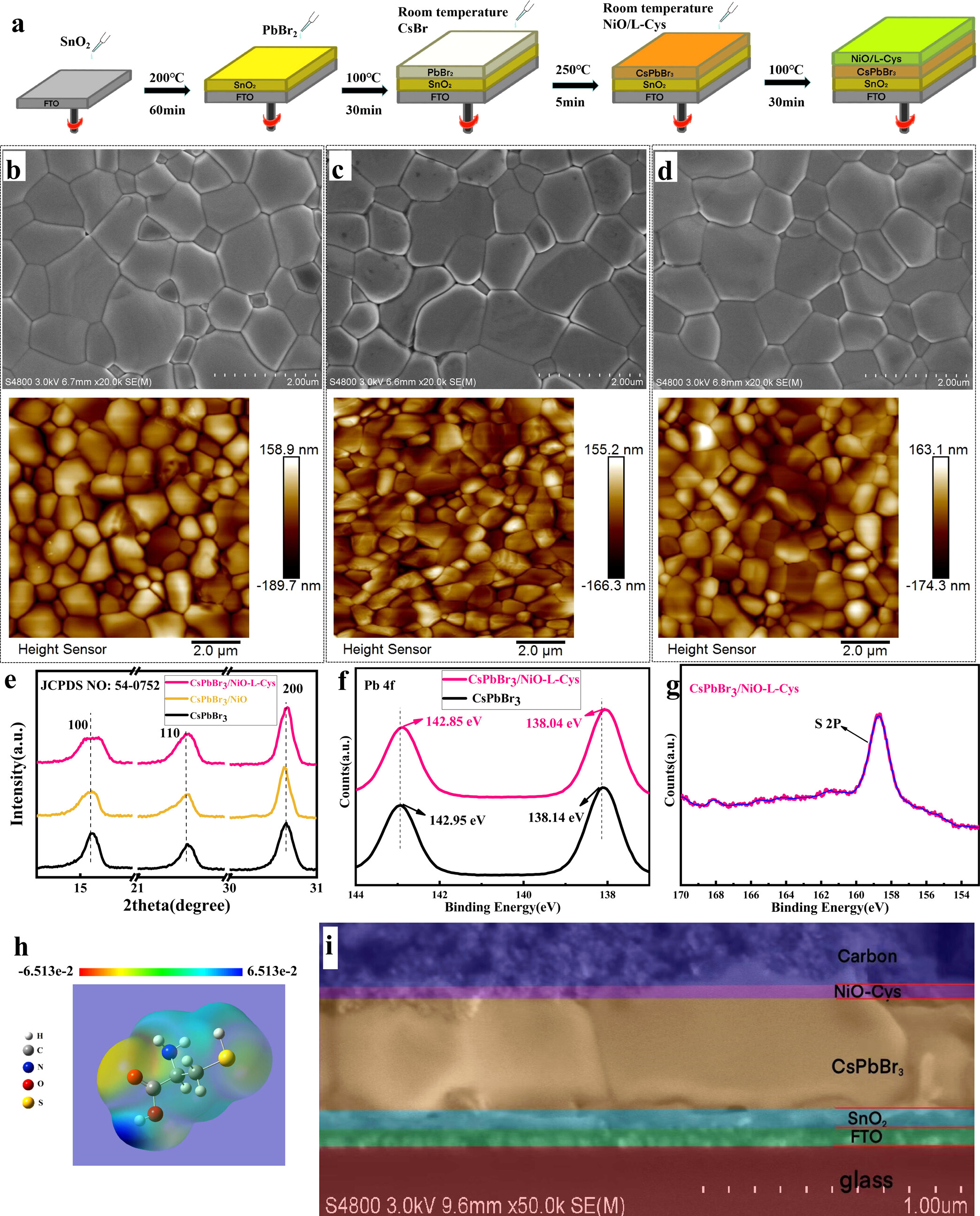
An FTO/SnO2/CsPbBr3/NiO-l-Cys/carbon perovskite solar cell device constructed by a multistep spin-coating method is shown in Figure 1a, and the details can be found in the Experimental Section. The cross-sectional scanning electron microscopy (SEM) image (Figure 1i) shows a seamless connection between the perovskite and carbon electrode layers. Excitons are generated after sunlight absorption by the CsPbBr3 perovskite layer and are divided into electrons and holes. The FTO glass collects electrons through the SnO2 electron transport layer. At the same time, the holes reach the carbon electrode through the nickel oxide hole transport layer, generating a current between the two electrodes. As depicted in Figure 1b–d, the perovskite film fabricated by the multiprocedure spin-coating approach shows compact and pinhole-free morphology. After altering the CsPbBr3 perovskite film with NiO and NiO-l-Cys, the mean crystal grain size remains almost unchanged, while the grain boundary gap narrows and the perovskite film is smooth and dense. AFM images of the perovskite films reveal root-mean-square (RMS) values of 42.2, 35.9, and 39.6 nm for the pristine CsPbBr3 perovskite film, modified film with NiO, and modified film with NiO-l-Cys, respectively. These results corroborate the improved flatness. Notably, the nickel oxide modified by l-Cys (Figure 1d) possesses better morphology than nickel oxide (Figure 1c), consistent with the transmission electron microscopy (TEM) image (Figure S1 of the Supporting Information). These micromorphological changes indicate reduced defects in the CsPbBr3 perovskite film after NiO-l-Cys deposition, displaying an inhibited nonradiative recombination process and enhanced charge transport performance. During annealing, the C3H7NO2S molecules (Figure S2) anchor to the CsPbBr3 perovskite surface owing to the interaction between the S atom-containing lone pair of electrons and unharmonious positively charged ions (Pb2+ and Cs+). The role of the defect passivation effect was further studied by preparing a Cys-free hole transport layer.
Figure 1
Figure 1. (a) Schematic illustration of the multistep spin-coating method to fabricate the CsPbBr3 thin film. Top-view SEM and AFM images of (b) CsPbBr3, (c) CsPbBr3/NiO-l-Cys, and (d) CsPbBr3/NiO-Cys films. (e) XRD patterns of CsPbBr3, CsPbBr3/NiO, and CsPbBr3/NiO-Cys films. XPS spectra of (f) Pb 4f and (g) S 2p in NiO-Cys-modified CsPbBr3 films. (h) Electrostatic potential mapping (ESP) image of the l-Cys molecule. (i) Cross-sectional SEM image of the typical FTO/SnO2/CsPbBr3/NiO-l-Cys/carbon device structure.
Since the quality of absorbing layer films would directly affect the carrier transport performance and optical absorption quality, the CsPbBr3 crystal phase was further characterized to clarify the role of NiO and NiO-l-Cys in the perovskite films. In Figures 1e and S3, three feature peaks are observed at 2θ = 15.2, 21.7, and 26.5, corresponding to (100), (110), and (111) facets of perovskite stage (JCPDS No: 54-0752), respectively. Thus, the perovskite structure does not change after depositing the hole transport layer on the perovskite surface. Nevertheless, the characteristic peaks shift to higher angles, meaning a decreased lattice constant, (30) caused by the lattice contraction induced by a smaller ion radius of Ni2+ (0.69 Å) compared to that of Pb2+ (1.190 Å), validating the partial substitution of Pb2+ by Ni2+ ions. The contracted lattice volume is favorable to stabilizing the perovskite (more proper τ value) and generating more energy. (31)
The surface chemical states and cooperation between l-Cys and perovskite films were further investigated by XPS characterization (Figure S4). Compared to CsPbBr3, the binding energy of Pb 4f7/2 in CsPbBr3/NiO-Cys changed from 138.14 to 138.04 eV, while that of Pb 4f5/2 decreased from 142.95 to 142.87 eV (high-resolution graphs in Figure 1f). (32,33) According to the lower binding energy of Pb 4f, the lone pair of electrons of the S or N elements of Cys interacts with the CsPbBr3 lattice. The peak of S 2p at 158.7 eV in Figure 1g is attributed to the Pb–S bond. Since S is significantly smaller than Br, S is embedded in the CsPbBr3 perovskite lattice gap instead of replacing Br, causing the perovskite lattice expansion. (34,35) As seen in Figure S5, the N 1s peak of the l-Cys molecule is located at 399.89 eV and attributed to deprotonated -NH2, suggesting the adsorption of N atoms of l-Cys on the perovskite film surface. (36) In Figure S6, the EDS test mapping corroborates the XPS data, further confirming the existence of Ni, S, and O elements in the CsPbBr3/NiO-Cys film.
The overall electron allocation on the l-Cys surface was obtained by calculating the electrostatic potential mapping (ESP, Figure 1h). The color change from red to blue indicates a reduction in the charge density from −6.513 × 10⁻² to 6.513 × 10². The higher electron density of the l-Cys molecule is induced by a more negative ESP of –COOH, determining whether –COOH can preferentially combine with –OH on NiO. (37,38) The –SH groups interact with Pb to form a strong coordination linkage between l-Cys and CsPbBr3 because S atoms donate electrons to the oxygen vacancy. XRD and XPS show l-Cys acting as an interfacial chemical bridge between NiO and the CsPbBr3 perovskite film for an improved interface association.
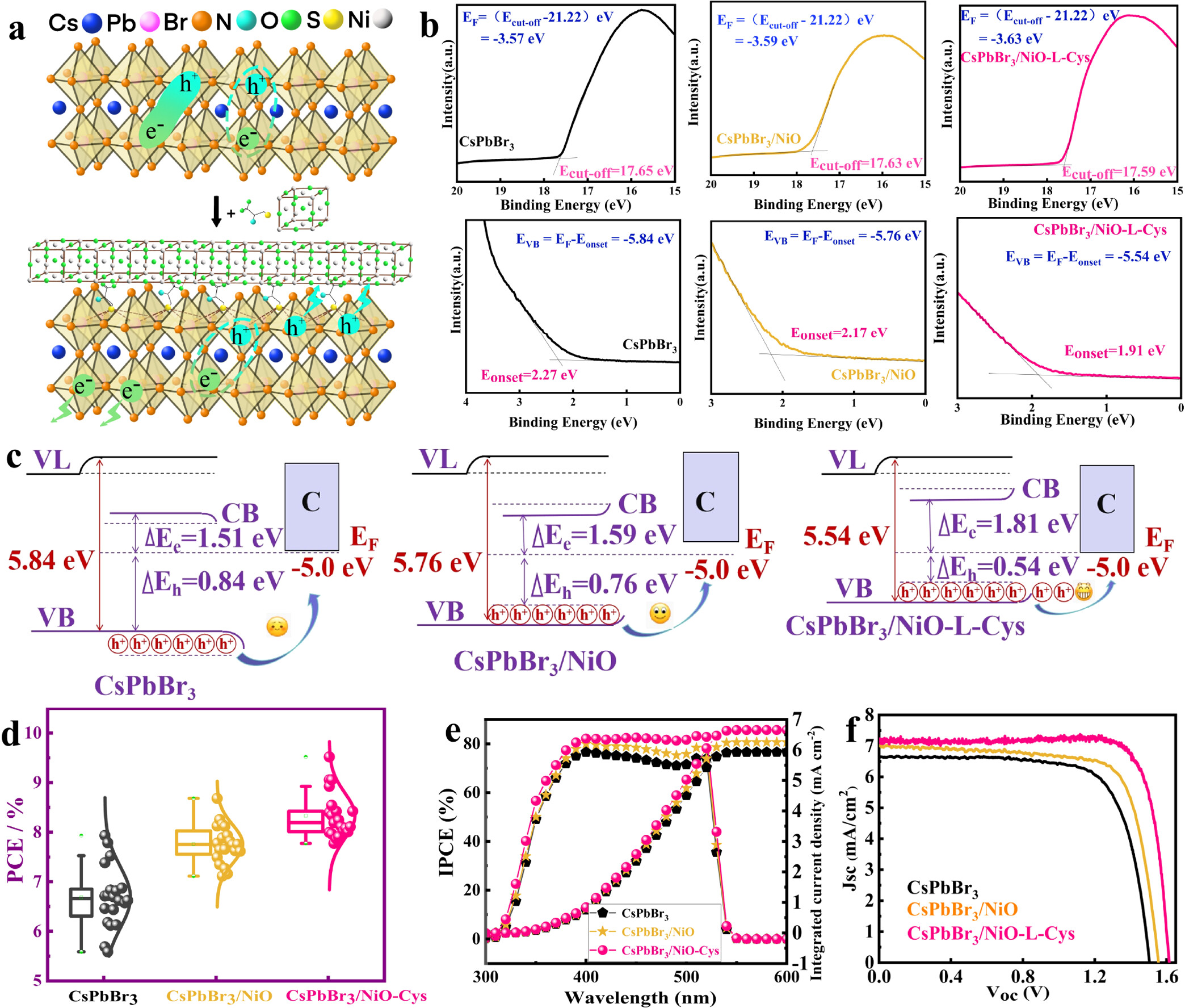
The integrated XPS, ESP, and XRD spectra reveal l-Cys’ association at the perovskite/NiO interface. In general, l-Cys can interact with the NiO side via –COOH and the perovskite side through -SH through chemical bridging at the perovskite/NiO interface. Such bilateral associations affect the interface properties, leading to enhanced contact performance and interface charge extraction/passivation. The roles of such a heterojunction interface in photovoltaic performance were further investigated by constructing all-inorganic PSCs with a configuration of FTO/SnO2/CsPbBr3 or (NiO or NiO-l-Cys)/carbon. Compared to the control CsPbBr3 device, the PCEs of NiO-l-Cys-altered PSCs show an enhancement (Figure 2d). As summarized in Table 1, the tailored CsPbBr3/NiO-l-Cys PSC realizes a maximum PCE of 9.61% with a VOC of 1.614 V, a short-circuit current density (JSC) of 7.23 mA·cm–2, and a fill factor (FF) of 82.2% (J–V curves, Figure 2f) under sunlight irradiation. These values are much greater than those of the control device with a typical PCE of 7.35%, a short-circuit current (JSC) of 6.65 mA·cm–2, a VOC of 1.504 V, and a fill factor of 73.50%, demonstrating the universality of NiO-l-Cys for improved device efficiency (Table S1). The photovoltaic parameters in Figures 2d and S7 revealed excellent repeatability and high performance of the NiO-l-Cys device with greatly suitable outcomes in IPCE spectra (Figure 2e) and stable power outputs (Figure 4d). In particular, significantly increased VOC was obtained for the CsPbBr3/NiO-l-Cys device. Since the splitting of quasi-Fermi degrees and reintegration inside the perovskite would control the VOC, (39) the improvement can be caused by control of the interface exposed to the upper perovskite film when considering the nearly unvaried morphology and optical transmittance of the underlying ETL on the FTO substrate. This was confirmed by the optimized energy structure associated with an interfacial charge extraction–transfer action.
Figure 2
Figure 2. (a) Exciton behavior of CsPbBr3 films with and without NiO/l-Cys. (b) Energy-level diagrams of the charge-transfer process. (c) Energy-level diagrams of interfacial charge transfer in various PSCs. (d) PCE distribution of CsPbBr3, CsPbBr3/NiO, and CsPbBr3/NiO-l-Cys-tailored PSCs. (e) IPCE and integrated current densities and (f) J–V curves of various PSCs.
Table 1. Photovoltaic Parameters of the Devices Tailored by CsPbBr3, CsPbBr3/NiO, and CsPbBr3/NiO-Cys Perovskite Films
perovskite film
Voc (V)
Jsc (cm·mA–2)
FF (%)
PCE (%)
CsPbBr3
1.504
6.65
73.50
7.35
CsPbBr3/NiO
1.555
7.02
74.90
8.18
CsPbBr3/NiO-l-Cys
1.614
7.24
82.20
9.61
UPS testing of CsPbBr3, CsPbBr3/NiO, and CsPbBr3/NiO-l-Cys films was used to identify the evolution of interfacial energetics. The binding energy cutoff (Ecutoff) and binding energy onset (Eonset) are illustrated in Figure 2b. The corresponding work function values (WFs) and valence band maximum (EVB) values of CsPbBr3, CsPbBr3/NiO, and CsPbBr3/NiO-Cys films are 3.57, 3.59, and 3.63 eV and −5.84, −5.76, and −5.54 eV, respectively, calculated by the equation: WFs = 21.2 eV – Ecutoff and EVB = −WFs – Eonset. (40,41) The energy level value of carbon is about −5.0 eV. (42) Thus, p-type doping of NiO greatly conforms to previous reports, (43) and the energy barrier for hole extraction from perovskite is found to be greatly decreased. Furthermore, the detailed energy-level diagrams are illustrated in Figure 2c, which show the conduction band (CB) and the valence band (VB) of CsPbBr3, CsPbBr3/NiO, and CsPbBr3/NiO-Cys films based on the Eonset and bandgaps derived from Figure S8. From the optimized interfacial energy structure, such as the conversion from downward band-bending to upward band-bending owing to an up-shifted EF of CsPbBr3, CsPbBr3/NiO, and CsPbBr3/NiO-Cys films, the increased energy difference between the CB of CsPbBr3, CsPbBr3/NiO, and CsPbBr3/NiO-Cys and the EF of carbon (ΔEe) (1.51, 1.59, vs 1.81 eV) and the reduced energy difference between the VB of CsPbBr3, CsPbBr3/NiO, and CsPbBr3/NiO-Cys and the EF of carbon (ΔEh) (0.84, 0.76, vs 0.54 eV), the hole accumulation in the perovskite film is effectively suppressed, thus reducing the recombination loss and improving the voltage output. (37) The schematic diagram of carrier dynamics in the perovskite and hole transport layer interfaces is illustrated in Figure 2a. The excitons in the optimized perovskite film are separated and transferred smoothly, inhibiting the charge recombination.
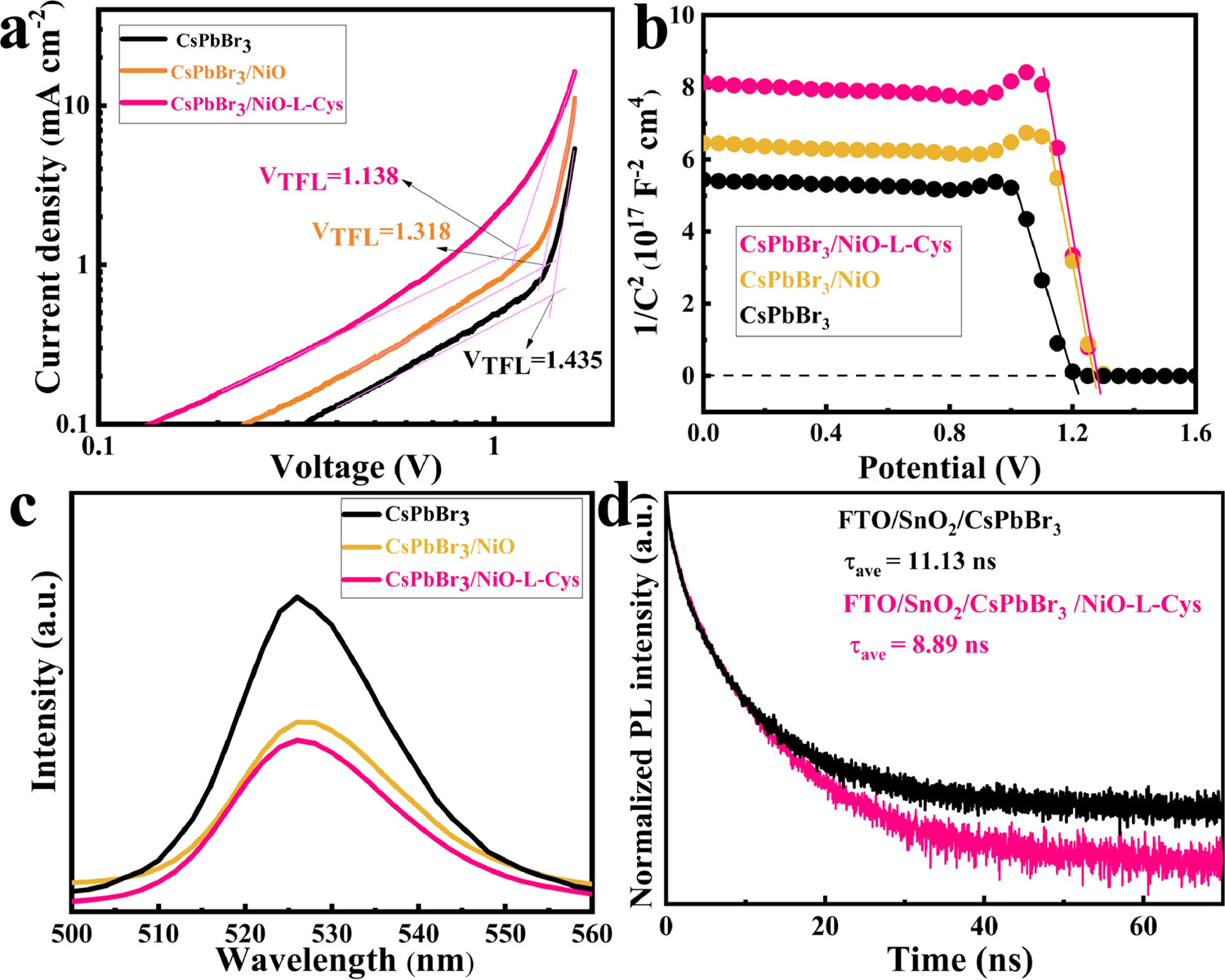
Since the interfacial charge extraction–transfer behavior is highly dependent on the disadvantageous flaws generated during conversion and crystal development, the trap-state density (ntrap) of each perovskite film was quantized by space-charge-limited current (SCLC) measurements under dark conditions and electron-only structures (Figure 3a). ntrap can be calculated from the onset voltage (VTFL) of the trap-filled limit region using eq 1: (44)
??trap=2????0??TFL/(????2)
(1)
where e represents the primary charge, L and ε represent the thickness and relative dielectric constant of the CsPbBr3 film, respectively, and ε0 indicates the vacuum permittivity. The calculations reveal remarkably decreased ntrap values from 2.65 × 10¹⁶ for the control CsPbBr3 device to 8.75 × 10¹⁵ and 7.55 × 10¹⁵ for the CsPbBr3 layer modified with NiO and NiO-l-Cys, respectively. Hence, the perovskite films possess reduced trap states. The influence of NiO-l-Cys alternation on carrier reintegration kinetics was clarified by exciting the films by using a laser at a wavelength of 385 nm. The PL and TRPL spectra in Figure 3c,d show opposite responses to traditional PL quenching in the CsPbBr3/NiO-l-Cys-based perovskite film. The quenched PL intensity is related to the presence of Cys, which enhances the interface contact of perovskite/NiO by forming chemical bonding, further driving the interfacial electron extraction. (45) The mean carrier lifetime (τave) can be calculated by eq 2: (46)
??ave=(??1??12+??2??22)/(??1??1+??2??2)
(2)
where τ1 represents the fast decay time caused by electron extraction by the hole transport layer and τ2 reveals the slow decay time related to trap reintegration in the bulk perovskite film. A1 and A2 indicate their amplitudes. As shown in Table S2, the CsPbBr3/NiO-l-Cys-based perovskite film displayed a shorter τave (8.89 ns) than that of the CsPbBr3-based perovskite film (11.13 ns). Therefore, the Cys alternation may drive the interface charge extraction according to the grown built-in electric field (Vbi, Figure 3b) originating from the capacitance–voltage (C–V) curves based on the Mott–Schottky equation, eq 3: (47)
??2=2(??bi??)/(??2????0????)
(3)
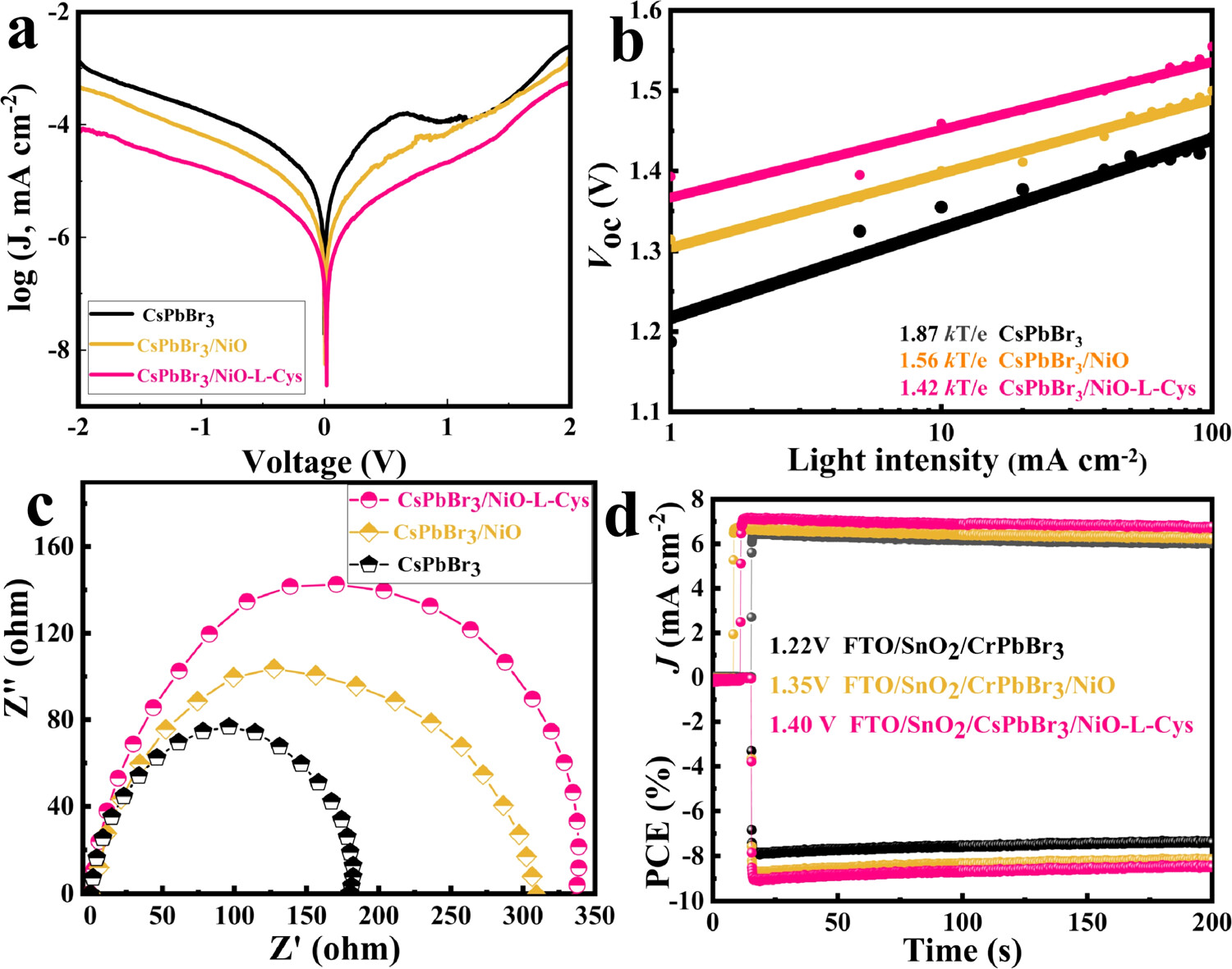
where A refers to the active surface, e represents the primary charge, ε denotes the related dielectric constant of the perovskite, ε0 depicts the vacuum permittivity, and N represents the doping density of the perovskite. Compared to the control device, the CsPbBr3/NiO-l-Cys-tailored device exhibits a higher Vbi, suitable for better diode characteristics of PSCs. Also, the leakage current of CsPbBr3/NiO-l-Cys is significantly suppressed when compared to the control device (Figure 4a). The light-intensity dependence curves of VOC in Figure 3b are evaluated by eq 4: (48)
??OC=??????ln(??)/??
(4)
Figure 3
Figure 3. (a) Dark J–V curves of FTO/ETL/CsPbBr3 (CsPbBr3/NiO or CsPbBr3/NiO-l-Cys)/PCBM/carbon devices. (b) Nyquist plots of various PSCs measured in the dark. (c) Stable-state PL spectra and (d) time-resolved PL (TRPL) decay curves of CsPbBr3 films with and without NiO-l-Cys modification.
Figure 4. (a) Dark J–V curves of various PSCs. (b) Relationship between the light intensity and Voc. (c) Nyquist plots and fitting lines of various devices. (d) Stabilized efficiency measurements at a fixed bias potential of 1.4 V for FTO/ETL/CsPbBr3 (CsPbBr3/NiO or CsPbBr3/NiO-l-Cys)/carbon devices.
The VOC is directly proportional to the logarithm of I, and n refers to an ideal element related to monomolecular reintegration. T, k, and q represent the absolute temperature, Boltzmann constant, and elemental charge, respectively. The Shockley–Read–Hall (SRH) level and bimolecular reintegration are lower for smaller slope values. (49,50) According to Figure 4b, the slope of the control device is estimated to be (1.87) kT/e. By comparison, lower slopes of (1.56) and (1.42) kT/e are recorded for the devices modified with CsPbBr3/NiO and CsPbBr3/NiO-l-Cys, respectively. Hence, the lower disadvantageous flaw leads to recombination restraining due to decreased unharmonious Pb2+ in the CsPbBr3 film. Meanwhile, the NiO-l-Cys-altered device displays a greater Rrec value (400 Ω) than the control CsPbBr3 PSC device (Rrec of 340 Ω), indicating a greatly controlled charge reintegration in PSCs (Figure 4c). The higher Rrec values originating from the smaller trap-state density can stop the charge recombination and drive carrier extraction in the PSC device. Thus far, it is concluded that the CsPbBr3/NiO-l-Cys structure induced energy degree control and defect reduction synergistically decide the enhanced VOC.
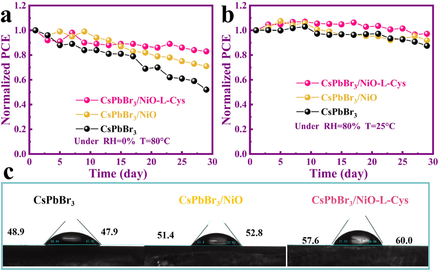
The PCE longevity tests of PSC devices with and without NiO-l-Cys are compared in Figure 5a,b. The optimal PSC without encapsulation maintains 83% of the initial PCE after 30 days of storage in air with 0% relative humidity (RH) and a temperature of 80 °C. By comparison, the control PSC shows obvious degradation with a loss of 48% of its initial PCE. Meanwhile, the humidity stability of unencapsulated devices is evaluated at a high RH of 80% and 25 °C and displays a stronger humidity resistance of CsPbBr3 /NiO-l-Cys devices after 30 days of aging, equivalent to a conservation rate of 98%. This value is higher than that of the control device (87%). The expanded contact angle from 48.9 to 60.0 indicates a higher degree of hydrophobicity for the CsPbBr3 /NiO-l-Cys film (Figure 5c). By fabricating this all-in-one film to heal the CsPbBr3/NiO-l-Cys interface effectively, the interface defects are suppressed to trigger phase degradation, thereby improving the long-term stability of the self-encapsulation devices.
Figure 5
Figure 5. Long-term stability of encapsulation-free devices with CsPbBr3, CsPbBr3-NiO, and CsPbBr3-NiO-Cys under an air environment with (a) 0% relative humidity and a temperature of 80 °C and (b) 80% relative humidity and a temperature of 25 °C. (c) Enlarged contact angles of the CsPbBr3, CsPbBr3-NiO, and CsPbBr3-NiO-Cys films.
In conclusion, the p-type doping of NiO decreases the energy-level barrier and the CsPbBr3/NiO-l-Cys interface, forming chemical bonds, stopping the charge recombination, and driving the interface charge-carrier extraction. This combination effectively enhances the photoelectric performance of all-inorganic CsPbBr3 PSCs, achieving a champion PCE of 9.61% with a higher VOC of 1.614 V. Furthermore, the increased NiO-l-Cys perovskite film quality effectively enhanced the long-term stability of the unencapsulated device, and the robust stability of the device under prolonged exposure to high humidity and temperature conditions highlights its potential for practical applications. These findings provide valuable insights into enhancing the interface properties and perovskite film quality for efficient and stable PSCs.


