


Abstract
Broadband achromatic metalenses and metalens arrays hold promise for enabling high-performance optical imaging in a compact form factor. Conventional visible-light achromatic metalenses are composed of transparent and high-refractive-index TiO2 or GaN nanopillars, but are strongly limited in mainstream silicon-based complementary metal-oxide-semiconductor (CMOS) processes. Herein, we report the realization of high-efficiency Si3N4 achromatic metalenses in the visible range and demonstrate their integration onto a commercial imaging chip. By improving nanofabrication techniques, we have dramatically increased the aspect ratio of Si3N4 nanostructures from ~17 to a high value of 43.33. Consequently, the group delay of the Si3N4 nanostructures is significantly increased and the averaged focusing efficiency of a Si3N4 metalens with a numerical aperture of 0.155 reaches 80.39%. Owing to the CMOS-compatibility of Si3N4, such high-quality metalenses have been integrated with commercial imaging sensors and demonstrated the capability of full-color optical imaging. This research paves a critical step towards chip-integrated meta-devices.
Introduction
Lenses are integral components of optical systems and are widely used in many industries including automotive, electronics, healthcare and telecommunications. The rapid development of emerging technologies such as medical imaging and augmented reality has brought about the demand for ultracompact and integrated optical lenses, and has spawned the research field of metalenses1,2,3,4,5,6,7,8,9. Metalens is a planar photonic device that is composed of nanoantennas and has the diffraction-limited focusing capabilities10,11,12,13,14,15,16,17,18,19. In principle, the periodic lattice and optical resonances greatly increase the dispersion of the metalens, leading to more severe chromatic aberration than its bulky counterpart20,21,22. Soon after the advent of metalenses, chromatic aberration has attracted considerable research attention and great efforts were made to eliminate it. In 2018, using high-refractive-index dielectrics such as TiO2 and GaN, the visible-light broadband achromatic metalens was experimentally demonstrated, and a series of applications such as full-color imaging, light-field imaging, and hyperspectral imaging were developed from this23,24,25,26,27,28. Despite the progress in miniaturization of optical system, the deposition of TiO2 and GaN membranes typically requires temperature higher than 600 °C, strongly restricting the direct integration of such metalens on top of conventional integrated circuits (IC) chip29,30.
Silicon nitrides (Si3N4) is another transparent material with a high refractive index in the visible light range. High quality Si3N4 membrane can be deposited with plasma enhanced chemical vapor deposition (PECVD) at a relatively low temperature31,32. Meanwhile, Si3N4 nanostructures can be easily achieved with conventional processes of the mature IC industry33,34,35. As a consequence, Si3N4 has been widely used in various microelectronic and photonic chips. It is also a reasonable idea to use Si3N4 to prepare achromatic metalenses. On the one hand, Si3N4 is compatible with CMOS and can be mass-produced, which can greatly reduce the cost of achromatic metalenses and bring their prices close to the price range of traditional optical devices. On the other hand, low-temperature processing technology allows achromatic metalenses to be directly integrated into traditional IC chips, which will greatly promote the practical application of such planar photonic devices. Although some efforts have been made recently, the device performances of Si3N4 achromatic metalenses are still restricted. This is because the refractive index of Si3N4 is much lower than TiO2 and GaN, and the nanofabrication technique only allows an aspect ratio around 10-1736,37,38,39,40,41. The library of meta-atom is thus strongly limited and the transmittance (focusing efficiency) must be sacrificed to fulfill the required group delay42,43. So far, high-performance Si3N4 achromatic metalenses remain technically challenging and absent (details in Supplementary Note 1). Here, we report the improvement of Si3N4 nanofabrication technique and the realization of high-efficiency Si3N4 achromatic metalenses in the visible range. Their direct integration onto a commercial imaging chip and the corresponding full-color imaging have also been demonstrated.
Results
Numerical design of Si3N4 achromatic metalens
Figure 1(a) illustrates a schematic diagram of the integrated imaging system. It is an achromatic metalens integrated onto a commercial CMOS imaging sensor. The metalens is composed of Si3N4 nanopillars with different profiles that can support a spatial and frequency-dependent phase profiles following the equation24

where c, r, ω, and F are the speed of light, radial coordinates, angular frequency, and focal length, respectively. To achieve achromatic focusing within a frequency range around ??, it is well-known that both the relative phase φ(?,??) and relative group delay ∂φ(?,?)/∂? should be satisfied at least. In principle, when the extremes of dispersion are represented at the center and edge of the metalens, the required range of group delay is defined as the group delay difference at the center and edge of the metalens, which is closely related to the numerical aperture (NA), the radius, and achromatic bandwidth of the metalens. Consequently, the minimal group delay is determined once the NA and size of achromatic metalens are pre-defined (details in Supplementary Note 2).
Fig. 1: The design and the performance of the Si3N4 achromatic metalens.
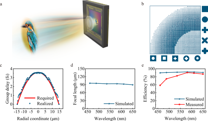
a Schematic of the broadband Si3N4 achromatic metalens showing the principle of integral imaging. b The layout of the quarter of the designed metalens. Ten fundamental building blocks are enlarged at the edge. c The required group delay for broadband achromatic metalens with NA = 0.155 (solid line) and the values provided by the Si3N4 meta-units (dots). d Numerically calculated focal length of the metalens at different wavelengths. e Numerically calculated (dots) and experimental measured (squares) efficiency of the metalens at different wavelengths. The diameter of metalens is fixed at 30 µm.
In design, both the phase and group delay are provided by Si3N4 nanopillars. Without considering the mode coupling and end-facet reflection, the phase of transmitted light through each Si3N4 nanopillar can be simplified to φ(?,?)=???????, where neff and h are the effective refractive index and the pillar height. Then the group delay at position r can be expressed as

It is obvious that both the phase and the range of relative group delay is proportional to the product of the effective refractive index and pillar height. The effective refractive index is determined by the ratio of electromagnetic waves inside dielectrics and in air and varies between n = 1 (air) and n ~ 2 (Si3N4) by controlling the in-plane morphology of nanopillar. As a consequence, the group delay range and corresponding size and NA of the achromatic metalens depends directly on the pillar height and aspect ratio. The group delay dispersion (GDD, which means the derivative of group delay with respect to diagonal frequency) will also increase by increasing the height to 1300 nm. However, the linear fitting metric ???????2 for all the selected nanopillars keeps exceed 0.997, confirming that the influence of GDD is smaller and can be not considered within the 200 nm bandwidth centered at 510 nm in our design.
In numerical simulation, ten types of meta-units, including squares, circles, crosses, concentric overlays of circles and crosses, petal shapes and their corresponding anti-structures were employed as building blocks of the metalens (Fig. 1b). Each shape has at least C4 rotational symmetry and thus the dependence on the incident polarization has been eliminated. Parameter sweeps of the meta-units size and shape were conducted to build a library that provides values for phase, group delay, and transmittance in the entire visible spectrum with a step of 2 nm (see three examples in Supplementary Fig. S2). For the fixed shapes, the increase of pillar height has a double advantage. It greatly enlarges the range of group delay (Supplementary Fig. S3) and allows a better fitting to the required values. Meanwhile, more nanopillars can provide similar phase and group delay and thus a higher transmittance can also be selected, closely relating to the focusing efficiency of achromatic metalens.
To fit the nanofabrication capability, we restrict the pillar height to h = 1300 nm and the minimal feature size to 40 nm. Figure 1c–e shows the numerical results of an achromatic metalens with a NA of 0.155. It is obviously that the required group delay has been satisfied (Fig. 1c). As a consequence, the incident light with wavelength from 460 nm to 650 nm have been focused to the same position around F = 93.5 μm with a variation below 1.6% (Fig. 1d). Figure 1e shows the numerically calculated focusing efficiency (the ratio of the energy at the focus to the energy at the incident beam) across the visible spectrum. We can see that the efficiency varies slightly around 90% and gives an average value of 91.2%. All these results are consistent with the above analysis and demonstrate that high-performance visible-light achromatic metalens can also be realized with Si3N4 if the nanofabrication technique is improved to ensure the designed pillar height and aspect ratio (comparison details with other metalenses are shown in Supplementary Note 1).
Fabrication of high quality Si3N4 metalens
A crucial step towards high-performance Si3N4 achromatic metalens lies in the nanofabrication technology. Recent progress shows Si3N4 nanostructures with height up to 1250 nm can be fabricated38. The aspect ratio, however, is only around 10 to 17, resulting in a restricted focusing efficiency (36–55%) and a small NA of 0.08613. To realize the designed meta-devices, we have developed a top-down etching technology. The Si3N4 film is deposited at a low temperature of 200 °C using plasma enhanced chemical vapor deposition (PECVD, Oxford PlasmaPro 800). The deposition temperature is strictly controlled to be below 250 °C to prevent damage to the imaging detector on the wafer when preparing metasurfaces on CMOS surface in the future. The refractive index and light extinction coefficient are shown in Supplementary Fig. S5. The refractive index of Si3N4 film exceeds 2.02 in 460–650 nm wavelength range, while the light extinction coefficient approaches zero. All these results show that the Si3N4 film deposited at a low temperature is suitable for high-performance meta-devices.
The Si3N4 nanostructures are fabricated with a combined process of electron-beam (E-Beam) lithography and inductively coupled plasma (Oxford Plasmalab System 100, ICP180) etching. The schematic of fabrication is shown in Fig. 2a. In the first, a 50 nm Cr layer was deposited on it by electron beam evaporation. Next, the nanostructures were patterned using E-beam lithography and transferred to SiO2 via a typical lift-off process. The pattern was further transferred into the Cr layer using an ICP etching process with a selectivity up to 100:1. Then Si3N4 membrane was etched in ICP by taking Cr layer as a hard mask. Different from previous demonstrations, our approach uses the mixture of CHF3 and O2. The introduction of O and H ions can induce C and F ions to form a fluorocarbon protective layer on the Si3N4 surface, thereby achieving simultaneous etching and deposition, effectively reducing the surface roughness. Meanwhile, we dynamically adjust the ratio of CHF3 and O2 from 12.5 to 7.2 as depth increases so that fluorocarbons exist at a relatively stable thickness. This adjustment can effectively prevent the accumulation of fluorocarbon in the micro-grooves and maintain the anisotropy of the etching process. As a result, high quality Si3N4 nanostructures can be obtained (details in Supplementary Note 4).
Fig. 2: Fabrication of high-quality Si3N4 nanostructures.
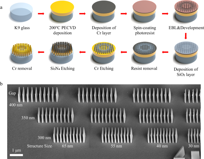
a Schematic diagram of the nanofabrication process. b The tilt-view SEM images of grating arrays with different duty cycles. The width of each nano-ridge reduces from 65 nm to 30 nm, respectively.
Taking the gratings as an example, we have tested our fabrication process. Figure 2b shows the tilt-view scanning electron microscope (SEM) images of Si3N4 gratings. Here the pillar height is 1300 nm. High quality Si3N4 nanostructures can be preserved by reducing the width of nano-ridges from ~ 65 nm to 30 nm. Obvious collapse of Si3N4 nanostructures can be found when the width of nano-ridge is below 20 nm. Similar high-quality nanofabrication is also applicable to two dimensional materials, e.g., Si3N4 nanopillars with different geometries (see Supplementary Fig. S8). Therefore, we can confirm that our process has the capability of fabricating Si3N4 nanostructures with a thickness of 1300 nm. The aspect ratio is calculated by fabricating a series of gratings with width from 65 nm to 30 nm and aspect ratio is calculated to 43.33 (see Supplementary Fig. S9-10 and Supplementary Movie 1). Compared to other top-down fabrication, this approach can provide a record high aspect ratio. Meanwhile, it offers significant advantages of meta-devices by being directly implemented on packaged CMOS detectors. This capability makes the process low-cost and semiconductor foundry compatibility, presenting considerable benefits for the development of flat optical systems in real applications.
Characterization of Si3N4 achromatic metalens
With the same process, the designed metalenses in Fig. 1 have been experimentally fabricated. Figure 3a–c display the corresponding top-view and tilt-view SEM images of one metalens with a designed NA of 0.155. It is easy to see that both the solid and inverse meta-units are well produced. Their locations, shapes and feature sizes are strictly in accordance with the numerical design (Fig. 3b). Meanwhile, the Si3N4 nanopillars have nearly vertical sidewalls (Fig. 3c), with the measured tilt angle of sidewalls approximately 89−90°. All these results indicates that the designed phase, group delay, and efficiency for an achromatic metalens can be satisfied and realized in real samples.
Fig. 3: The experimentally fabricated Si3N4 metalens with NA = 0.155.
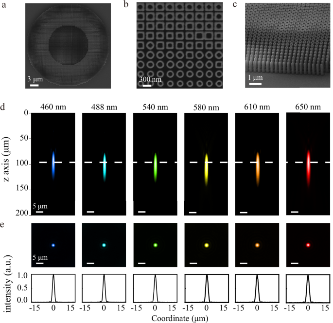
a, b are the top-view SEM images of achromatic metalens with different resolutions. Different types of meta-units can be clearly identified. c The corresponding tilt-view SEM image of the metalens. d, e are the intensity profiles of focal spots in x-z plane and x-y planes at different wavelengths. The white dashed line depicts the numerical focal length. The bottom panels depict the normalized intensity profiles along the diameter. The intensity profiles have the same scale bar.
The optical properties of Si3N4 achromatic metalens are optically characterized using a home-made optical system (see Supplementary Fig. S12). The unpolarized supercontinuum laser is collimated and passed through a bandpass filter. The incident beam reaches the metalens from the substrate and is focused. To determine the focal length, the cross-sectional intensity profiles along the propagation direction has been recorded at different wavelengths and shown in Fig. 3d. With the increase of central wavelength from 460 nm to 650 nm, the brightest spots remain at a constant position, which is 97.33 μm away from the Si3N4 metalens with a variation of 5%. This focal length matches the numerical designed value (F = 93.5 μm, marked by white dashed line). Figure 3e shows the normalized intensity profiles of the focal spot in x-y plane at different wavelength. The full-widths at half-maximum (FWHMs) of intensity along the diameter of focal spot are very close to the diffraction limit (?/2??, see Supplementary Fig. S16). Meanwhile, the corresponding Strehl ratios remains at a high value of 0.88 across the entire visible spectrum. By measuring the transmitted power at the focal spot and the incident power, the focusing efficiency of metalens has also been measured and plotted in Fig. 1e. An average efficiency of 80.39% has been experimentally obtained across the entire spectral range. This value is a record for visible-light achromatic metalens, but is still slightly lower than the numerically design. Considering the largest reduction occurs at shorter wavelength, this degradation might be caused by three factors, i.e., size variation, imperfect sidewall, and surface roughness and can be potentially improved (details in Supplementary Note 5).
The capability of full-color imaging of achromatic metalens has been experimentally characterized as well. Figure 4a–f shows achromatic imaging of a 1951 United States Air Force (USAF) resolution test chart, highlighting a typical resolvable structure illuminated by lights with wavelengths ranging from 460 nm to 650 nm. The smallest resolved feature had a linewidth of 2.19 μm (group 7, element 5 and element 6), determined by the Rayleigh criterion and the measured FWHM shown in Fig. 3e, indicating the precise fabrication of the achromatic metalens. Moreover, the small efficiency variation though the viable wavelength will reduce color differences, enabling the creation of realistic full-color images through our achromatic metalens without compensating the intensity at three preliminary colors. Figure 4g–i present the full-color images formed through our achromatic metalens, captured by a CCD without any additional intensity compensation for three preliminary colors. Compared to the original pictures (available in Supplementary Fig. S17), the color images appeal reliable and closely match originals. The images in Fig. 4 demonstrate the effectiveness of eliminating the chromatic effect across the entire visible spectrum and enable rapid recording of true-color images.
Fig. 4: Imaging using the achromatic metalens with NA = 0.155.
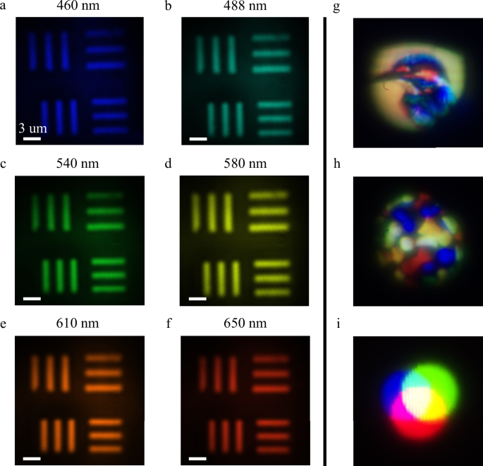
a–f The images of element 5 and 6, group 7 of the 1951 Unites States Air Force resolution target recorded by the achromatic metalens at different wavelengths. The images have the same scale bar. g–i The full-color images formed by the achromatic metalens without color correction.
Integration of Si3N4 achromatic metalens array on a CMOS chip
Based on the above demonstrations, we further integrate the Si3N4 achromatic metalens onto a CMOS image sensor. For a fixed pillar height of 1300 nm, the working principle of achromatic metalens restricts its size and NA to small values. To improve the image quality and fit the commercial device, a 5×5 metalens array have been fabricated and mounted on the chip (Fig. 5a). Figure 5b shows a microscope image of the metalens array at 10× magnification. Each metalens has a diameter of 90 μm. The designed focal length and NA are 980 μm and 0.046, respectively. Then the optical properties of all metalenses have been measured. The average focusing efficiencies, focal lengths and NA values in the visible spectrum are summarized in Fig. 5c–e. The detailed information can be seen in Supplementary Note 9. We can see that all the metalenses have almost identical focal length and NA at the designed values. The average focusing efficiency also remains as a constant around 67% ± 2%.
Fig. 5: Light-field imaging with a metalens array.
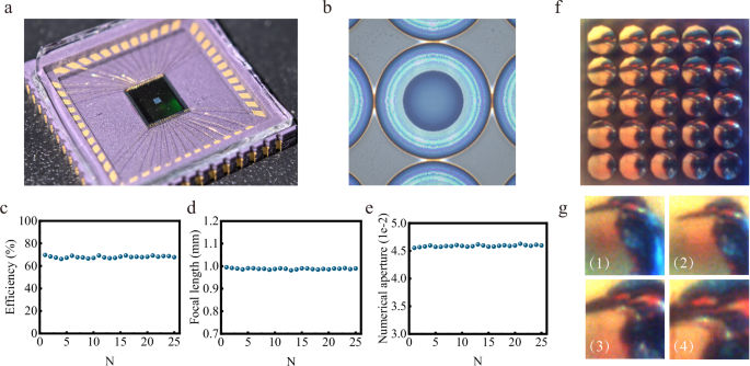
a The top-view optical microscope images of the metalens array. b The high-resolution top-view optical microscope images of single metalens. c–e are the measured averaged focusing efficiencies, focal lengths and numerical aperture for 25 separated single metalenses. f The raw light-field image with the achromatic metalens array. g The rendered images with color distortion and background subtraction. (1–4) represent different positions with different magnification rates of the original image respectively.
The high uniformity of the integrated metalens array allows for imaging without color cast. The colorful image can be directly obtained on the imaging plan, located precisely on the CMOS sensor surface. The achromatic metalens array forms 25 sub-images with ~90 μm in size, offering different perspectives of the projected object as shown in Fig. 5f. Each sub-image is clear and easy to distinguish without overlay with each other. A commercial panoramic image stitching software, PTGui, is used to create a high-quality composite image from these sub-images (details in Supplementary Note 10). Figure 5g presents the reconstructed images after correcting color distortion and background subtraction without losing the resolution (5 μm in linewidth of group 6, element 5, as shown in Supplementary Fig. S22). As the object magnification increases, the sensor image can still be directly recorded, producing clear, colorful light-field image that conform our integrated achromatic metalens array can effectively break the restriction between achromatic bandwidth and wide FOV. Since this stitched image covers an area 1.8 times larger than that of a single metalens without decreasing the resolution, efficiency and achromatic performance, the array can be easily expanded to cover much larger areas, potentially encompassing the entire CMOS sensor. The metalens array is further fabricated directly on top of the sensor using Direct Laser Writing to in-situ polymerize a polymer film (details in Supplementary Note 12), confirming that the deposition of the Si3N4 and the etching process have no adverse effect on the performance of the image sensors and the Si3N4 meta-units can be well fabricated as designed. This approach can enable wide FOV integral and achromatic imaging through the entire visible wavelength range.
Discussion
In summary, we have developed an approach to fabricate high quality Si3N4 achromatic metalens in the visible spectrum. The improved nanofabrication process can produce Si3N4 nanostructures with a record-breaking aspect ratio. As a consequence, the group delay range of Si3N4 nanopillars are increased and the key performances of metalens in focusing efficiency and NA have been significantly improved too. The nanofabrication techniques are stable and reproducible. Achromatic metalens array with nearly identical performances has been experimentally demonstrated and combined to a commercial CMOS imaging sensor. As a consequence, high performance full color image has been achieved with a single metalens or an integrated metalens array. Since all processes are conducted at low temperature with low electron beam energy, sensor integrity is maintained, ensuring that imaging performance is fully protected. The direct integration of Si3N4 meta-units on top of CMOS chip has also been carried out. The integrated achromatic Si3N4 metalens array holds promise for the mass manufacture of high-performance, next-generation optical devices based on metasurfaces.
Methods
Numerical simulations
To fulfill the phase compensation requirements for different positions of the metalens, a comprehensive meta-units library with various structural parameters is established. The transmission and phase spectra result for all meta-units are simulated using Reticolo, a rigorous coupled-wave analysis (RCWA) solver. The Si3N4 meta-unit has a height of 1300 nm and the meta-unit periodicity is set as 350 nm. For each simulation, a sweep parameter is utilized to obtain the phase spectrum, with the wavelength varying from 460 nm to 650 nm. A linear fit is utilized to analyze the phase spectrum in order to calculate the group delay and the spectral reference phase at the zero frequency. To demonstrate the focusing performance of the achromatic metalens, finite-domain time-difference simulations (Lumerical FDTD Solutions) are utilized to model the metalens. Perfectly matched layer (PML) boundary conditions are applied along both transverse and longitudinal directions under plane wave illumination.
Film deposition
The 1300-nm-thick high-quality Si3N4 film is deposited onto the K9 optical glass substrate with plasma enhanced chemical vapor deposition (PECVD) in a mixture of SiH4, NH3 and N2 gas. The deposition rate is 6.5 nm/min and the deposition temperature is 200 °C. The optical parameters are measured using spectroscopic ellipsometer and shown in Supplementary Fig. S5. By adjusting the silicon-nitrogen ratio during deposition, the refractive index of the film can be obtained to be approximately 2.02 through the whole visible wavelength, while the loss can be ignored.
Device fabrication
After the deposition of Si3N4 film, 50-nm-thick Cr layer is deposited on the film used the E-beam evaporator. Subsequently, the PMMA A2 e-beam resist is spin-coated onto the Cr layer and baked at 180 °C for 15 min. The sample is then exposed through the electron-beam lithography system (Raith E-line Plus) and the patterns are revealed after the development process in MIBK/IPA. Following this, 20-nm-thick SiO2 layer is deposited as hard mask to etch the Cr layer on the sample using the E-beam evaporator. The pattern is transferred to SiO2 through a lift-off process using PG Remover. Next, the patterns are transferred to the Cr layer by inductively coupled plasma etching (Oxford PlasmalabSystem100, ICP180) in a mixture of Cl2 and O2 gas. The patterns are then transferred to Si3N4 film using Cr as the hard mask by ICP in a mixture of CHF3 and O2 gas. As the etching depth increases, adjustments are made to the ratio of CHF3/O2 from 12.5 to 7.2, effectively improving anisotropic etching and achieving high aspect ratio silicon nitride meta-units etching. The final metalens can be obtained after removal of the Cr hard etching mask.
Optical characterization
In order to verify the performance of the broadband achromatic metalens, we built a home-made optical system. Details of the optical experimental setup for characterizing the broadband achromatic metalens are shown in Supplementary Note 6. The sample is moved 0.1 μm per step by a motion control module (Kinesis® K-Cube) controlled by Labview to record the intensity distributions along z-axis.
For the purpose of accurately evaluating the focusing efficiency of the metalens, we measured the power concentrated in the focal spot. This is determined by measuring the power of the transmitted light that passed through a circular area with a radius of 3×FWHM of the focal spot. We then divide this by the power of the incident light, which is measured as the power of the incident light passing through a circular area with the same radius as the metalens.
Data availability
The data that support the plots within this paper and other findings of this study are available from the corresponding author on request.