


Please enter the answer below before you can view the full text.
4+1=
The sensibility of a waveguide evanescent wave sensor is limited by its evanescent wave intensity. To improve the sensibility of the sensor, the evanescent wave intensity of the waveguide was enhanced by designing a high-refractive-index resin layer on the surface of the waveguide. To optimize the layer thickness, the relationship between the evanescent wave ratios and the layer thicknesses under different refractive index values was studied. A laser-induced waveguide self-written technique was utilized to fabricate an evanescent wave sensor by coating a layer on the waveguide with refractive index of 1.6 and a thickness of 300 nm, respectively. The UV-Vis spectral measurement results show that after the layer coating, the absorption detection limit of Rhodamine B aqueous solution is increased to 1×10⁻⁹ g/mL, which is 10 times enhanced than that of the uncoated sensor. The sensor has the merits of low cost, small size, simple fabrication and high sensitivity, which has broad application prospects in various fields.
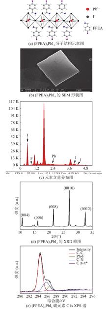
The environmental factors, such as light radiation, water vapor, and oxygen, induce the degradation of two-dimensional perovskites, and therefore its stability greatly limits the further development and marketization of this material. Taking advantage of the strong stability and hydrophobicity of fluoride, fluorophenylethylamine was introduced into the organic layer of two-dimensional perovskites, which could effectively improve the stability of two-dimensional perovskites, but the fluorescence efficiency was partly reduced. To solve this problem, polystyrene (PS), polymethylmethacrylate (PMMA) and cycloolefin polymer (COP) were employed to encapsulate the two-dimensional perovskite film. The photoluminescence intensity was improved by 2.2, 1.3 and 1.4 times, respectively. The light stability was improved by 3.3, 3.1 and 3.9 times, respectively. Furthermore the humidity stability was also verified. This study provides a new idea for the development of two-dimensional perovskite films in optoelectronic devices.
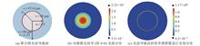
To improve the sensitivity of optical waveguide sensor based on evanescent wave sensing, a kind of high-refractive-index film coated waveguide optical fiber sensor is proposed by simulation and verified by experiment. In this study, we propose an optical fiber-waveguide-fiber EF sensing platform, which composes of a Ta2O5 coated polymer waveguide sandwiched by two multimode optical fibers, to enhance the intensity of evanescent wave and increase the sensitivity of the sensor. Through simulation results, the Ta2O5 film thickness was optimized. We selected 70 nm, 100 nm and 150 nm thickness for the coating experiments. With the coating thickness of 100 nm, we achieved absorption spectrum limit of detection for Rh B of 1×10⁻⁸ g/mL. The sensor has the advantages of low cost, small volume, simple manufacture and high sensitivity, which can be widely used in various fields.
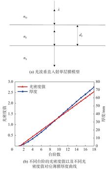
Ni80Cr20 alloy film shows a good neutral transmission in visible light. The quartz crystal sensor in the coating machine has a system error, which results in the actual thickness being different from the standard value. To solve this problem, a new manufacturing method for controlling film thickness of neutral density filters was proposed in this paper, which is bombarded the membrane surface with low energy ion beams. Make the relative error of optical density value is controlled within ±2%, and the absolute error is not more than ±0.01. The error of the thickness of the film is controlled at the atomic layer scale, which meets the requirements of the use of the filter in the spectral system with high precision. It is verified that the neutral density filter still has good optical properties and surface flatness after ion beam etching in this experiment. The technology of ion beam bombardment etching becomes a new and reliable method to control the thin film thickness.