


 View fulltext
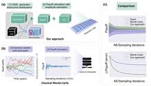
A photonic integrated chip for option pricing achieves precise market capturing and computational speedup through generative adversarial learning and quantum amplitude estimation algorithm. It is a step forward in specialized photonic processors to improve the efficiency and quality of financial applications. See Hui Zhang et al., pp. 1703-1712.
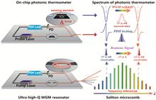
Soliton microcomb-assisted microring photonic thermometer with ultra-high resolution and broad range
Cheng Zhang, Jin Wang, Guoguo Kang, Jianxin Gao, Zhier Qu, Shuai Wan, Chunhua Dong, Yijie Pan, and Jifeng Qu
Whispering gallery mode resonators (WGMRs) have proven their advantages in terms of sensitivity and precision in various sensing applications. However, when high precision is pursued, the WGMR demands a high-quality factor usually at the cost of its free spectral range (FSR) and corresponding measurement range. In this article, we propose a high-resolution and wide-range temperature sensor based on chip-scale WGMRs, which utilizes a Si3N4 ring resonator as the sensing element and a MgF2-based microcomb as a broadband frequency reference. By measuring the beatnote signal of the WGM and microcomb, the ultra-high resolution of 58 micro-Kelvin (μK) was obtained. To ensure high resolution and broad range simultaneously, we propose an ambiguity-resolving method based on the gradient of feedback voltage and combine it with a frequency-locking technique. In a proof-of-concept experiment, a wide measurement range of 45 K was demonstrated. Our soliton comb-assisted temperature measurement method offers high-resolution and wide-range capabilities, with promising advancements in various sensing applications.
Photonics Research
Sep. 21, 2023Vol. 11 Issue 10 A44 (2023)
Julius Kullig, Daniel Grom, Sebastian Klembt, and Jan Wiersig
Exceptional points are degeneracies in the spectrum of non-Hermitian open systems where at least two eigenfrequencies and simultaneously the corresponding eigenstates of the Hamiltonian coalesce. Especially, the robust construction of higher-order exceptional points with more than two degenerate eigenfrequencies and eigenstates is challenging but yet worthwhile for applications. In this paper, we reconsider the formation of higher-order exceptional points through waveguide-coupled microring cavities and asymmetric backscattering. In this context, we demonstrate the influence of perturbations on the frequency splitting of the system. To generate higher-order exceptional points in a simple and robust way, a mirror-induced asymmetric backscattering approach is used. In addition to the exceptional-point enhanced sensing capabilities of such systems, also a cavity-selective sensitivity is achieved for particle sensing. The results are motivated by an effective Hamiltonian description and verified by full numerical simulations of the dielectric structure.
Photonics Research
Oct. 01, 2023Vol. 11 Issue 10 A54 (2023)

Fiber Optics and Optical Communications
Alireza Fardoost, Fatemeh Ghaedi Vanani, Sethumadhavan Chandrasekhar, and Guifang Li
Light propagation in random media is a subject of interest to the optics community at large, with applications ranging from imaging to communication and sensing. However, real-time characterization of wavefront distortion in random media remains a major challenge. Compounding the difficulties, for many applications such as imaging (e.g., endoscopy) and focusing through random media, we only have single-ended access. In this work, we propose to represent wavefronts as superpositions of spatial modes. Within this framework, random media can be represented as a coupled multimode transmission channel. Once the distributed coherent transfer matrix of the channel is characterized, wavefront distortions along the path can be obtained. Fortunately, backreflections almost always accompany mode coupling and wavefront distortions. Therefore, we further propose to utilize backreflections to perform single-ended characterization of the coherent transfer matrix. We first develop the general framework for single-ended characterization of the coherent transfer matrix of coupled multimode transmission channels. Then, we apply this framework to the case of a two-mode channel, a single-mode fiber, which supports two randomly coupled polarization modes, to provide a proof-of-concept demonstration. Furthermore, as one of the main applications of coherent channel estimation, a polarization imaging system through single-mode fibers is implemented. We envision that the proposed method can be applied to both guided and free-space channels with a multitude of applications.
Sep. 21, 2023Vol. 11 Issue 10 1627 (2023)
Image Processing and Image Analysis
Zhihong Zhang, Kaiming Dong, Jinli Suo, and Qionghai Dai
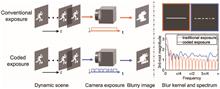
Coded exposure photography is a promising computational imaging technique capable of addressing motion blur much better than using a conventional camera, via tailoring invertible blur kernels. However, existing methods suffer from restrictive assumptions, complicated preprocessing, and inferior performance. To address these issues, we proposed an end-to-end framework to handle general motion blurs with a unified deep neural network, and optimize the shutter’s encoding pattern together with the deblurring processing to achieve high-quality sharp images. The framework incorporates a learnable flutter shutter sequence to capture coded exposure snapshots and a learning-based deblurring network to restore the sharp images from the blurry inputs. By co-optimizing the encoding and the deblurring modules jointly, our approach avoids exhaustively searching for encoding sequences and achieves an optimal overall deblurring performance. Compared with existing coded exposure based motion deblurring methods, the proposed framework eliminates tedious preprocessing steps such as foreground segmentation and blur kernel estimation, and extends coded exposure deblurring to more general blind and nonuniform cases. Both simulation and real-data experiments demonstrate the superior performance and flexibility of the proposed method.
Sep. 27, 2023Vol. 11 Issue 10 1678 (2023)
Instrumentation and Measurements
Zihang Peng, Yijun Huang, Kaiyuan Zheng, Chuantao Zheng, Mingquan Pi, Huan Zhao, Jialin Ji, Yuting Min, Lei Liang, Fang Song, Yu Zhang, Yiding Wang, and Frank K. Tittel
Nanophotonic waveguides hold great promise to achieve chip-scale gas sensors. However, their performance is limited by a short light path and small light–analyte overlap. To address this challenge, silicon-based, slow-light-enhanced gas-sensing techniques offer a promising approach. In this study, we experimentally investigated the slow light characteristics and gas-sensing performance of 1D and 2D photonic crystal waveguides (PCWs) in the near-IR (NIR) region. The proposed 2D PCW exhibited a high group index of up to 114, albeit with a high propagation loss. The limit of detection (LoD) for acetylene (C2H2) was 277 parts per million (ppm) for a 1 mm waveguide length and an averaging time of 0.4 s. The 1D PCW shows greater application potential compared to the 2D PCW waveguide, with an interaction factor reaching up to 288%, a comparably low propagation loss of 10 dB/cm, and an LoD of 706 ppm at 0.4 s. The measured group indices of the 2D and 1D waveguides are 104 and 16, respectively, which agree well with the simulation results.
Sep. 21, 2023Vol. 11 Issue 10 1647 (2023)
Integrated Optics
Xiuyou Han, Xinxin Su, Meng Chao, Xindi Yang, Weiheng Wang, Shuangling Fu, Yicheng Du, Zhenlin Wu, and Mingshan Zhao
In-band full-duplex (IBFD) technology can double the spectrum utilization efficiency for wireless communications, and increase the data transmission rate of B5G and 6G networks and satellite communications. RF self-interference is the major challenge for the application of IBFD technology, which must be resolved. Compared with the conventional electronic method, the photonic self-interference cancellation (PSIC) technique has the advantages of wide bandwidth, high amplitude and time delay tuning precision, and immunity to electromagnetic interference. Integrating the PSIC system on chip can effectively reduce the size, weight, and power consumption and meet the application requirement, especially for mobile terminals and small satellite payloads. In this paper, the silicon integrated PSIC chip is presented first and demonstrated for IBFD communication. The integrated PSIC chip comprises function units including phase modulation, time delay and amplitude tuning, sideband filtering, and photodetection, which complete the matching conditions for RF self-interference cancellation. Over the wide frequency range of C, X, Ku, and K bands, from 5 GHz to 25 GHz, a cancellation depth of more than 20 dB is achieved with the narrowest bandwidth of 140 MHz. A maximum bandwidth of 630 MHz is obtained at a center frequency of 10 GHz. The full-duplex communication experiment at Ku-band by using the PSIC chip is carried out. Cancellation depths of 24.9 dB and 26.6 dB are measured for a bandwidth of 100 MHz at central frequencies of 12.4 GHz and 14.2 GHz, respectively, and the signal of interest (SOI) with 16-quadrature amplitude modulation is recovered successfully. The factors affecting the cancellation depth and maximum interference to the SOI ratio are investigated in detail. The performances of the integrated PSIC system including link gain, noise figure, receiving sensitivity, and spurious free dynamic range are characterized.
Sep. 21, 2023Vol. 11 Issue 10 1635 (2023)
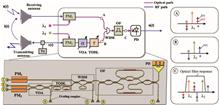
Efficient option pricing with a unary-based photonic computing chip and generative adversarial learningOn the Cover
Hui Zhang, Lingxiao Wan, Sergi Ramos-Calderer, Yuancheng Zhan, Wai-Keong Mok, Hong Cai, Feng Gao, Xianshu Luo, Guo-Qiang Lo, Leong Chuan Kwek, José Ignacio Latorre, and Ai Qun Liu
In the modern financial industry system, the structure of products has become more and more complex, and the bottleneck constraint of classical computing power has already restricted the development of the financial industry. Here, we present a photonic chip that implements the unary approach to European option pricing, in combination with the quantum amplitude estimation algorithm, to achieve quadratic speedup compared to classical Monte Carlo methods. The circuit consists of three modules: one loading the distribution of asset prices, one computing the expected payoff, and a third performing the quantum amplitude estimation algorithm to introduce speedups. In the distribution module, a generative adversarial network is embedded for efficient learning and loading of asset distributions, which precisely captures market trends. This work is a step forward in the development of specialized photonic processors for applications in finance, with the potential to improve the efficiency and quality of financial services.
Sep. 27, 2023Vol. 11 Issue 10 1703 (2023)
Yuqi Zhang, Qiang Luo, Dahuai Zheng, Shuolin Wang, Shiguo Liu, Hongde Liu, Fang Bo, Yongfa Kong, and Jingjun Xu
The ability to amplify optical signals is of paramount importance in photonic integrated circuits (PICs). Recently, lithium niobate on insulator (LNOI) has attracted increasing interest as an emerging PIC platform. However, the shortage of efficient active devices on the LNOI platform limits the development of optical amplification. Here, we report an efficient waveguide amplifier based on erbium and ytterbium co-doped LNOI by using electron beam lithography and an inductively coupled plasma reactive ion etching process. We have demonstrated that signal amplification emerges at a low pump power of 0.1 mW, and the net internal gain in the communication band is 16.52 dB/cm under pumping of a 974 nm continuous laser. Benefiting from the efficient pumping facilitated by energy transfer between ytterbium and erbium ions, an internal conversion efficiency of 10% has been achieved, which is currently the most efficient waveguide amplifier under unidirectional pumping reported on the LNOI platform, to our knowledge. This work proposes an efficient active device for LNOI integrated optical systems that may become an important fundamental component of future lithium niobate photonic integration platforms.
Sep. 28, 2023Vol. 11 Issue 10 1733 (2023)

Lasers and Laser Optics
Zhiyong Jin, Heming Huang, Yueguang Zhou, Shiyuan Zhao, Shihao Ding, Cheng Wang, Yong Yao, Xiaochuan Xu, Frédéric Grillot, and Jianan Duan
This work experimentally and theoretically demonstrates the effect of excited state lasing on the reflection sensitivity of dual-state quantum dot lasers, showing that the laser exhibits higher sensitivity to external optical feedback when reaching the excited state lasing threshold. This sensitivity can be degraded by increasing the excited-to-ground-state energy separation, which results in a high excited-to-ground-state threshold ratio. In addition, the occurrence of excited state lasing decreases the damping factor and increases the linewidth enhancement factor, which leads to a low critical feedback level. These findings illuminate a path to fabricate reflection-insensitive quantum dot lasers for isolator-free photonic integrated circuits.
Sep. 27, 2023Vol. 11 Issue 10 1713 (2023)
A. Bartolo, N. Vigne, M. Marconi, G. Beaudoin, L. Le Gratiet, K. Pantzas, I. Sagnes, A. Garnache, and M. Giudici
We show that a III-V semiconductor vertical external-cavity surface-emitting laser (VECSEL) can be engineered to generate light with a customizable spatiotemporal structure. Temporal control is achieved through the emission of temporal localized structures (TLSs), a particular mode-locking regime that allows individual addressing of the pulses traveling back and forth in the cavity. The spatial profile control relies on a degenerate external cavity, and it is implemented due to an absorptive mask deposited onto the gain mirror that limits the positive net gain within two circular spots in the transverse section of the VECSEL. We show that each spot emits spatially uncorrelated TLSs. Hence, the spatiotemporal structure of the light emitted can be shaped by individually addressing the pulses emitted by each spot. Because the maximum number of pulses circulating in the cavity and the number of positive net-gain spots in the VECSEL can be increased straightforwardly, this result is a proof of concept of a laser platform capable of handling light states of scalable complexity. We discuss applications to three-dimensional all-optical buffers and to multiplexing of frequency combs that share the same laser cavity.
Sep. 28, 2023Vol. 11 Issue 10 1751 (2023)
Nanophotonics and Photonic Crystals
Yucong Yang, Yueyang Liu, Jun Qin, Songgang Cai, Jiejun Su, Peiheng Zhou, Longjiang Deng, Yang Li, and Lei Bi
Zero-index metamaterials (ZIMs) feature a uniform electromagnetic mode over a large area in arbitrary shapes, enabling many applications including high-transmission supercouplers with arbitrary shapes, direction-independent phase matching for nonlinear optics, and collective emission of many quantum emitters. However, most ZIMs reported to date are passive; active ZIMs that allow for dynamic modulation of their electromagnetic properties have rarely been reported. Here, we design and fabricate a magnetically tunable ZIM consisting of yttrium iron garnet (YIG) pillars sandwiched between two copper clad laminates in the microwave regime. By harnessing the Cotton–Mouton effect of YIG, the metamaterial was successfully toggled between gapless and bandgap states, leading to a “phase transition” between a zero-index phase and a single negative phase of the metamaterial. Using an S-shaped ZIM supercoupler, we experimentally demonstrated a tunable supercoupling state with a low intrinsic loss of 0.95 dB and a high extinction ratio of up to 30.63 dB at 9 GHz. We have also engineered a transition between the supercoupling state and the topological one-way transmission state at 10.6 GHz. Our work enables dynamic modulation of the electromagnetic characteristics of ZIMs, enabling various applications in tunable linear, nonlinear, quantum, and nonreciprocal electromagnetic devices.
Sep. 14, 2023Vol. 11 Issue 10 1613 (2023)
Optical and Photonic Materials
You-Long Chen, Yi-Hua Hu, Xing Yang, You-Lin Gu, Xin-Yu Wang, Yu-Hao Xia, Xin-Yuan Zhang, and Yu-Shuang Zhang
Graphene quantum dots (GQDs), fascinating semiconductors with stable photoluminescence (PL), have important potential applications in the fields of biology, medicine, and new semiconductor devices. However, it is still challenging to overcome the weak PL intensity. Here, we report a strategy for selective resonance enhancement of GQD fluorescence using gold nanoparticles (AuNPs) as plasmas. Interestingly, the addition of low concentration AuNP makes AuNP/GQDs exhibit significant fluorescence enhancement of 2.67 times in the visible range. The addition of high concentration AuNP leads to the formation of an excitation peak at 421 nm and selectively enhances certain radiation modes. We concluded that the main reason for the selective enhancement of PL intensity in high concentration AuNP is the transfer of generous hot electrons at high energy states from AuNP to GQD and relaxation to the ground state. The electron resonance of low concentration AuNP transfers to GQD and relaxes to lower energy levels, exhibiting an overall enhancement of PL intensity. We apply it for detection of the heavy metal ion Cr3+, and verify that it has a correlation coefficient of 97.36%. We believe AuNP/GQDs can be considered excellent candidates for heavy metal detection and high fluorescence bio-imaging.
Oct. 01, 2023Vol. 11 Issue 10 1781 (2023)
Optical Devices
Xinyu Liu, Shaoxiong Wu, Xiaoxue Cao, Feng Tian, Srikrishna Chanakya Bodepudi, Muhammad Malik, Chao Gao, Li Peng, Huan Hu, and Yang Xu
Graphene-based photodetectors have attracted much attention due to their unique properties, such as high-speed and wide-band detection capability. However, they suffer from very low external quantum efficiency in the infrared (IR) region and lack spectral selectivity. Here, we construct a plasmon-enhanced macro-assembled graphene nanofilm (nMAG) based dual-band infrared silicon photodetector. The Au plasmonic nanostructures improve the absorption of long-wavelength photons with energy levels below the Schottky barrier (between metal and Si) and enhance the interface transport of electrons. Combined with the strong photo-thermionic emission (PTI) effect of nMAG, the nMAG–Au–Si heterojunctions show strong dual-band detection capability with responsivities of 52.9 mA/W at 1342 nm and 10.72 mA/W at 1850 nm, outperforming IR detectors without plasmonic nanostructures by 58–4562 times. The synergy between plasmon–exciton resonance enhancement and the PTI effect opens a new avenue for invisible light detection.
Sep. 21, 2023Vol. 11 Issue 10 1657 (2023)
Jie Jiang, Bo Fang, Chenxia Li, Zhi Hong, and Xufeng Jing
Optical metasurfaces are two-dimensional ultrathin devices based on single-layer or multilayer arrays of subwavelength nanostructures. They can achieve precise control of phase, amplitude, and polarization on the subwavelength scale. In this paper, a substrate-free all-silicon coded grating is designed, which can realize the phase control of the outgoing beam after the y-polarized plane wave is vertically incident on the metasurface at 0.1 THz. Through a single-layer silicon nanoarray structure, a low-reflection anomalous transmission metasurface is realized, and a variety of different beam deflectors are designed based on these encoded gratings. We propose a coded grating addition principle, which adds and subtracts two traditional coded grating sequences to obtain a new coded grating sequence. The encoded supergrating can flexibly control the scattering angle, and the designed substrate-free all-silicon encoded grating can achieve a deflection angle of 48.59°. In order to verify the principle of coded grating addition, we experimented with cascade operation of two coded sequence gratings to obtain the flexible control of the terahertz beam of the composite supergrating. The principle of grating addition provides a new degree of freedom for the flexible regulation of the terahertz wavefront. At the same time, this method can be extended to the optical band or microwave band, opening up new ways for electromagnetic wave manipulation and beam scanning.
Sep. 28, 2023Vol. 11 Issue 10 1738 (2023)
Solution-processed halide perovskite microcavity exciton-polariton light-emitting diodes working at room temperatureSpotlight on Optics
Tianyu Liu, Peng Ran, Yirong Su, Zeng Chen, Renchen Lai, Weidong Shen, Yaoguang Ma, Haiming Zhu, and Yang (Michael) Yang
Exciton-polaritons offer the potential to achieve electrically pumped perovskite polariton lasers with much lower current thresholds than conventional photonic lasers. While optically pumped exciton-polaritons have been widely studied in halide perovskites, electrically-pumped polaritons remain limited. In this study, we demonstrate the use of a solution-processing strategy to develop halide perovskite polariton light-emitting diodes (LEDs) that operate at room temperature. The strong coupling of excitons and cavity photons is confirmed through the dispersion relation from angle-resolved reflectivity, with a Rabi splitting energy of 64 meV. Our devices exhibit angle-resolved electroluminescence following the low polariton branch and achieve external quantum efficiencies of 1.7%, 3.85%, and 3.7% for detunings of 1.1, -77, and -128 meV, respectively. We also explore devices with higher efficiency of 5.37% and a narrower spectral bandwidth of 6.5 nm through the optimization of a top emitting electrode. Our work demonstrates, to our knowledge, the first room-temperature perovskite polariton LED with a typical vertical geometry and represents a significant step towards realizing electrically pumped perovskite polariton lasers.
Oct. 01, 2023Vol. 11 Issue 10 1791 (2023)
Optoelectronics
Light-stimulated low-power artificial synapse based on a single GaN nanowire for neuromorphic computingEditors' Pick
Min Zhou, Yukun Zhao, Xiushuo Gu, Qianyi Zhang, Jianya Zhang, Min Jiang, and Shulong Lu
The fast development of the brain-inspired neuromorphic computing system has ignited an urgent demand for artificial synapses with low power consumption. In this work, it is the first time a light-stimulated low-power synaptic device based on a single GaN nanowire has been demonstrated successfully. In such an artificial synaptic device, the incident light, the electrodes, and the light-generated carriers play the roles of action potential, presynaptic/postsynaptic membrane, and neurotransmitter in a biological synapse, respectively. Compared to those of other synaptic devices based on GaN materials, the energy consumption of the single-GaN-nanowire synaptic device can be reduced by more than 92%, reaching only 2.72×10⁻¹² J. It is proposed that the oxygen element can contribute to the synaptic characteristics by taking the place of the nitrogen site. Moreover, it is found that the dynamic “learning-forgetting” performance of the artificial synapse can resemble the behavior of the human brain, where less time is required to relearn the missing information previously memorized and the memories can be strengthened after relearning. Based on the experimental conductance for long-term potentiation (LTP) and long-term depression (LTD), the simulated network can achieve a high recognition rate up to 90% after only three training epochs. Such few training times can reduce the energy consumption in the supervised learning processes substantially. Therefore, this work paves an effective way for developing single-nanowire-based synapses in the fields of artificial intelligence systems and neuromorphic computing technology requiring low-power consumption.
Sep. 27, 2023Vol. 11 Issue 10 1667 (2023)
Silicon Photonics
Shaoteng Wu, Lin Zhang, Rongqiao Wan, Hao Zhou, Kwang Hong Lee, Qimiao Chen, Yi-Chiau Huang, Xiao Gong, and Chuan Seng Tan
The development of an efficient group-IV light source that is compatible with the CMOS process remains a significant goal in Si-based photonics. Recently, the GeSn alloy has been identified as a promising candidate for realizing Si-based light sources. However, previous research suffered from a small wafer size, limiting the throughput and yield. To overcome this challenge, we report the successful growth of GeSn/Ge multiple-quantum-well (MQW) p-i-n LEDs on a 12-inch (300-mm) Si substrate. To the best of our knowledge, this represents the first report of semiconductor LEDs grown on such a large substrate. The MQW LED epitaxial layer is deposited on a 12-inch (300-mm) (001)-oriented intrinsic Si substrate using commercial reduced pressure chemical vapor deposition. To mitigate the detrimental effects of threading dislocation densities on luminescence, the GeSn/Ge is grown pseudomorphically. Owing to the high crystal quality and more directness in the bandgap, enhanced electroluminescence (EL) integrated intensity of 27.58 times is demonstrated compared to the Ge LED. The MQW LEDs exhibit EL emission near 2 μm over a wide operating temperature range of 300 to 450 K, indicating high-temperature stability. This work shows that GeSn/Ge MQW emitters are potential group-IV light sources for large-scale manufacturing.
Sep. 12, 2023Vol. 11 Issue 10 1606 (2023)
Harnessing self-heating effect for ultralow-crosstalk electro-optic Mach–Zehnder switchesEditors' Pick
Peng Bao, Qixiang Cheng, Jinlong Wei, Giuseppe Talli, Maxim Kuschnerov, and Richard V. Penty
This paper presents a novel approach to counterbalance free-carrier-absorption (FCA) in electro-optic (E-O) Mach–Zehnder interferometer (MZI) cells by harnessing the self-heating effect. We show insights on crosstalk limitations in MZIs with direct carrier-injection and provide a detailed design methodology on a differential phase shifter pair. Leveraging both free-carrier dispersion (FCD) and self-heating effects, our design enables arbitrary phase tuning with balanced FCA loss in the pair of arms, eliminating the need for additional phase corrections and creating ultralow crosstalk MZI elements. This neat design disengages from the commonly used nested structure, thus providing an opportunity of embedding tunable couplers for correcting imperfect splitting ratios given that only two are needed. We show that with the use of tunable directional couplers, a standard ±10 nm process variation is tolerated, while achieving a crosstalk ratio below -40 dB. By direct carrier injection in both arms, the proposed device operates at nanosecond scales and can bring about a breakthrough in the scalability of E-O switch fabrics, as well as other silicon integrated circuits that have stringent requirements for crosstalk leakage.
Oct. 01, 2023Vol. 11 Issue 10 1757 (2023)
Spectroscopy
Xiutao Lou, Yue Wang, Ning Xu, and Yongkang Dong
Laser absorption spectroscopy (LAS) has been widely used for unambiguous detection and accurate quantification of gas species in a diverse range of fields. However, up-to-date LAS-based gas sensors still face challenges in applications where gas concentrations change in a wide range, since it is extremely difficult to balance spectral analysis strategies for different optical thicknesses. Here we present laser vector spectroscopy that combines absorption spectroscopy with dispersion spectroscopy, simultaneously taking advantage of the former’s high sensitivity in the low-concentration region and the latter’s high linearity in the high-concentration region. In the proof-of-concept demonstration of acetylene measurement, it achieves a linear dynamic range of 6×10⁷ (R2>0.9999), which surpasses all other state-of-the-art LAS techniques by more than an order of magnitude, with the capability of highly accurate quantification retained. The proposed laser spectroscopic method paves a novel way of developing large-dynamic-range gas sensors for environmental, medical, and industrial applications.
Sep. 27, 2023Vol. 11 Issue 10 1687 (2023)
Surface Optics and Plasmonics
Mauro David, Davide Disnan, Elena Arigliani, Anna Lardschneider, Georg Marschick, Hanh T. Hoang, Hermann Detz, Bernhard Lendl, Ulrich Schmid, Gottfried Strasser, and Borislav Hinkov
Long-wave infrared (LWIR, 8–14 µm) photonics is a rapidly growing research field within the mid-IR with applications in molecular spectroscopy and optical free-space communication. LWIR applications are often addressed using rather bulky tabletop-sized free-space optical systems, preventing advanced photonic applications, such as rapid-time-scale experiments. Here, device miniaturization into photonic integrated circuits (PICs) with maintained optical capabilities is key to revolutionize mid-IR photonics. Subwavelength mode confinement in plasmonic structures enabled such miniaturization approaches in the visible-to-near-IR spectral range. However, adopting plasmonics for the LWIR needs suitable low-loss and -dispersion materials with compatible integration strategies to existing mid-IR technology. In this paper, we further unlock the field of LWIR/mid-IR PICs by combining photolithographic patterning of organic polymers with dielectric-loaded surface plasmon polariton (DLSPP) waveguides. In particular, polyethylene shows favorable optical properties, including low refractive index and broad transparency between ∼2 μm and 200 µm. We investigate the whole value chain, including design, fabrication, and characterization of polyethylene-based DLSPP waveguides and demonstrate their first-time plasmonic operation and mode guiding capabilities along S-bend structures. Low bending losses of ∼1.3 dB and straight-section propagation lengths of ∼1 mm, pave the way for unprecedented complex on-chip mid-IR photonic devices. Moreover, DLSPPs allow full control of the mode parameters (propagation length and guiding capabilities) for precisely addressing advanced sensing and telecommunication applications with chip-scale devices.
Sep. 27, 2023Vol. 11 Issue 10 1694 (2023)
Zi-Wen Zhang, Yu-Lu Lei, Juan-Feng Zhu, and Chao-Hai Du
Terahertz vortices prompt numerous advanced applications spanning classical and quantum communications, sensing, and chirality-based detection, owing to the inherent physical properties of terahertz waves and orbital angular momentum (OAM). Nonetheless, existing methodologies for generating terahertz vortices face challenges such as unalterable topological charges and intricate feed networks. To address these limitations, we propose a novel approach to generate multi-mode and tunable vortex beams based on chiral plasmons. Through eigenmode analysis, the uniform helical gratings are demonstrated to support chiral plasmons carrying OAM. By leveraging their vortex characteristics and introducing modulation into the periodic system, these chiral plasmons are alternatively diffracted into high-purity vortex radiations according to the Bragg law. To validate the theory, the vortex beam emitter is fabricated and measured in the microwave regime based on the modulated scheme. Experimental results confirm the emission of vortex beams with desirable phase distributions and radiation patterns. Our findings highlight the potential of chiral plasmons as seeds for tunable and compact vortex radiation, offering promising applications in tunable vortex sources.
Sep. 27, 2023Vol. 11 Issue 10 1723 (2023)
2D-to-3D buckling transformability enabled reconfigurable metamaterials for tunable chirality and focusing effectEditors' Pick
Donghai Han, Wenkang Li, Tao Sun, Min Liu, Xiaoming Chen, Hongyu Shi, Zhengjie Fan, Fanqi Meng, Liuyang Zhang, and Xuefeng Chen
Recently, multifarious deformation approaches in nature have promoted dynamic manipulation for electromagnetic (EM) waves in metamaterials, and those representative strategies are mainly focused on the modulation of spectral parameters. Several works have also achieved tunable phase-gradient meta-devices. Here, to broaden the modulation freedom of mechanical deformation, we initially propose two reconfigurable metamaterials consisting of mirrored S-shaped meta-atoms selectively bonded on biaxially pre-stretched substrates. Planar meta-atoms with spin-insensitive transmittance are buckled into 3D morphologies to break residual symmetries by releasing the stress and to facilitate spin-dependent transmittance under circularly polarized incidence. Owing to the geometric anisotropy of S-shaped meta-atoms along the x and y axes, 3D chiral meta-atoms exhibit discriminate circularly cross-polarized transmittance under opposite spins. The underlying physical mechanism reveals that EM resonance originates from the excitation of electric dipoles and magnetic dipoles, and their cross coupling finally triggers the chiral effects of 3D meta-atoms. By introducing the gradient-phase design that keeps unchanged under various strains, two types of meta-atoms with specified orientations are interleaved to design a double-foci metalens, and its 2D-to-3D morphology transformation shortens the focusing length and facilitates the intensity change of two foci. Our approach in designing reconfigurable EM metamaterials with 2D-to-3D buckling transformability can be further extended toward terahertz even optical wavebands, and it may assist with deriving more applicable multi-functionalities in the aspects of imaging, sensing, and holograms.
Oct. 01, 2023Vol. 11 Issue 10 1770 (2023)
© Copyright 2018-2021 | Chinese Laser Press.
All Rights Reserved 沪ICP备15018463号-20