


Please enter the answer below before you can view the full text.
7+6=
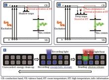
Persistent luminescent (PersL) materials, due to the unique delayed emission feature, have been extensively studied and applied in the fields of night-vision security, biological fluorescence labeling, optical information storage, and optical anti-counterfeiting. The application of PersL materials is closely related to the trap depth, in which the PersL materials used for the optical information storage need to have a larger trap depth to ensure a higher storage rate at room temperature. Optical information storage technology based on deep-trap PersL materials possesses excellent rewritability, low background, large storage capacity, and high design ability, notably showing great potential for the development of multidimensional optical information storage technology. It has thus become a significant research area for advanced optical materials. In this article, the background of deep-trap PersL materials for the optical information storage applications is briefly introduced. Then, the basic mechanisms of the information storage and reading based on the deep-trap charge carrier capture and release in PersL materials are given. The important breakthroughs and the latest progress of the deep-trap PersL material research are overviewed. Finally, the future development of deep-trap PersL materials is prospected.
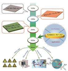
Long persistent phosphors show great superiority in the applications of biomedicine, energy, environment, and new technology fields owing to the unique separating process of optical excitation and emission, and they arouse wide interests of researchers in materials, chemistry, physics, and biomaterials fields. This review introduces the history and resurrected and thriving evolution process of long persistent phosphors. In addition, this review also elaborates the important timing points, key achievements, and main problems. We believe that the long persistent phosphors will rejuvenate with their unique charm and attract the researchers interested in the luminescence phenomenon to extend the past into the future and continue to renovate.
The highly integrated luminescence modes of inorganic luminescent materials provide opportunities for their multi-functional applications and interdisciplinary development. The multimodal luminescence mediated by energy traps is mainly based on the processes of carrier trapping and releasing. The carriers in a trap can escape from this trap under the stimulation of heat, light, or force, and subsequently recombine to produce thermos-luminescence, photo-stimulated luminescence, or mechano-luminescence. The multimodal luminescent materials with excellent photo-physical properties show potential applications in anti-counterfeiting, optical data storage, human-computer interaction, biomedicine, and so on. Herein, we reviewed the mechanism of multimodal luminescence, summarized the mechanism of trap filling and emptying, sorted out the research progress of energy-trap-dependent multimodal inorganic luminescent materials, and prospected the development trend of multimodal luminescent materials.
Long-afterglow phosphor is a unique photoluminescent energy-saving material having widespread applications in the areas of displays, biomedicine, energy, and environmental engineering. Sr2MgSi2O7∶Eu2+,Dy3+, as representative silicate material, is one of the most promising long-afterglow phosphors owing to its excellent water resistance, good chemical stability, and long afterglow time. However, its further commerical application is limited by insufficient afterglow intensity, narrow emission bands, and unclear afterglow mechanism. In this review, we give a comprehensive introduction of the history of Sr2MgSi2O7∶Eu2+,Dy3+ long-afterglow phosphor. In addition, we summarize the recent advances of Sr2MgSi2O7∶Eu2+,Dy3+ in terms of afterglow mechanism and diverse applications, including safety signs, bio-imaging, and photocatalysts. Finally, the urgent problems to be solved and potential future directions of Sr2MgSi2O7∶Eu2+,Dy3+ are discussed.
Rare earth ions doped nanomaterials have excellent photon upconversion property, showing great promise in broad frontier applications like nanophotonics, bioimaging-guided therapy and life science. Unlike conventional luminescence, the orthogonal upconversion is a newly observed phenomenon in rare earth luminescent nanomaterials, which is able to yield different emission colors by altering the excitation conditions. This allows for the construction of nano-platform, which is significant for the relevant frontier applications. This review summarizes the latest research progresses of orthogonal luminescence of rare earth ions, and presents a thorough discussion on the core-shell structure design principles and its key role in spectral manipulation towards orthogonal emission as well as its various applications including full-color display, optical memory, anti-counterfeiting security and bioimaging-guided therapy. The limitations of orthogonal luminescence are commented and future development are also prospected.
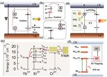
The afterglow properties of persistent luminescence materials depend on the trap energy level in materials. The afterglow modulation can be achieved by tuning trap depths for the proper capture ability of electrons or holes. Thermoluminescence is sensitive to the trap energy levels formed by impurities and lattice defects in semiconductors. It is an essential tool for the trap distribution analysis of persistent luminescence materials. Parameters such as the depth and density of the trap energy level in persistent luminescence materials can be quantitatively analyzed by measuring thermoluminescence spectra and adopting an appropriate spectral-curve analysis method. However, a well-accepted standard method for deducing the depth and density of traps from thermoluminescence spectra is still lacking. Herein, on the basis of the introduction of basic principles of thermoluminescence and thermoluminescence curve measurement, the peak shape characteristics of different kinetic models and their applicable conditions were first introduced. Then, the analysis methods of the thermoluminescence curve were summarized. Their applications in the analysis of trap characteristics of persistent luminescence materials were discussed after introducing thermoluminescence. The primary focus was on the application and research progress of the initial rise method.
Acousto-optic modulators have been widely used in many fields such as laser technology, network communication, and radar spectrum analyzer. As the key component of acousto-optic devices, various types of acousto-optic materials have been extensively studied.First, the basic theory of acousto-optic diffraction and the important performance parameters of acousto-optic materials, including diffraction efficiency, quality factor, and ultrasonic attenuation, are briefly summarized; second, the research progress of acousto-optic crystals and glass materials and their applications in the field of acousto-optic modulators are reviewed; finally, the research status of new acousto-optic materials in recent years is summarized and stated, pointing out the advantages and disadvantages of crystal and glass as commercial acousto-optic materials respectively, which provides reference for further improving the performance of acousto-optic devices and expanding their application fields.
Near-infrared phosphor conversion light-emitting diode (NIR pc-LED) is a new type of near infrared solid-state light source for detection; recently, core material broadband near-infrared phosphors have received enormous attention. Herein, the broadband near-infrared δ-Sc4Zr3O12∶Cr3+ phosphor was prepared by a high-temperature solid-state method. Under the excitation of blue light, the near infrared emission position is 810 nm and the FWHM of emission peak is approximately 175 nm. The broadband emission corresponds to the overlap of two emission peaks, and the positions of the two emission subpeaks correspond to 795 nm and 873 nm, respectively, which is reflected in the results of luminescence decay and temperature-dependent emission spectrum. The crystal field strength is estimated to be 2.25 determined using spectral data. Finally, the application of the prepared broadband near-infrared δ-Sc4Zr3O12∶Cr3+ phosphors in NIR pc-LED was explored.
Phosphor-converted light-emitting diodes (pc-LEDs) have great potential in near-infrared spectroscopy technology and near-infrared imaging technology. However, the development of novel broadband near-infrared phosphors remains a challenge. In this paper, a series of hexagonal phase structure Cs2NaAlF6∶Cr3+ near-infrared emission phosphors are prepared by an ammonium salt conversion method. Under 434 nm blue light excitation, the phosphors show a broadband near-infrared emission band peak at ~780 nm with full width at half maximum of 106 nm, and the luminescence intensity at 150 ℃ can maintain 68.4% of that at room temperature (25 ℃). Further, a broadband near-infrared pc-LED device is fabricated based on Cs2NaAlF6∶0.30Cr3+ phosphor and a blue LED chip. When the driving current is 1000 mA, a near-infrared output power of 226.49 mW is obtained in pc-LED device, and the corresponding energy conversion efficiency is 2.4%.The device may find application in veins imaging and other fields.
The efficiency of single-junction solar cells has a limitation due to the low energy of the solar spectrum and weak photon response in the high-energy region. The spectral mismatch loss is the main factor that limits the efficiency of solar cells. An effective way of reducing the spectral mismatch loss is using spectral conversion materials to convert photons in low response regions into photons in high response regions. Spectral conversion materials include up-conversion (UC), down-shifting (DS), and quantum cutting (QC) luminescent materials. In the UC process, multiple photons with energies lower than the bandgap of the solar cell are converted into higher-energy photons. In the DS process, a high-energy photon is converted into a low-energy photon. In the QC process, a high-energy photon is converted into multiple low-energy photons. These spectrally converted photons can be efficiently used by solar cells, improving their energy conversion efficiency. Therefore, this study summarizes the spectral adaptation conditions of different types of solar cells, details the latest research progress of UC, DS, and QC luminescent materials and give a prospect of the future development direction of using spectral conversion materials to improve the efficiency of solar cells.
As a new semiconductor material with advantages such as large absorption cross-section, long carrier diffusion length, high photoluminescence quantum yield (PLQY), color purity, and adjustable wavelength, metallic halide perovskite materials have been widely used in lighting and displays, solar cells, photoelectric detection, and bio-imaging, to name a few. However, some problems exist in the perovskite materials, such as the low PLQY of blue perovskite quantum dots (QDs), poor stability of red perovskite, and the toxicity of Pb2+, which limits their applications. Doped perovskite materials can help solve the aforementioned problems and further improve their optical/electrical properties. In this paper, the preparation of doped perovskite and the effects of ion doping or substitution at A-site, B-site, and X-site on the photoelectric performance and stability of metal halide perovskite are introduced. Finally, applications of the doped perovskite materials are summarized.
Owing to their excellent optical properties, fiber lasers and fiber amplifiers composed of rare-earth-doped fibers (also known as active fibers) are widely used in space, nuclear power, and high-energy physics facilities. However, in an irradiation environment, rare-earth-doped fibers are vulnerable to radiation-induced loss and their optical performance deteriorates rapidly. Therefore, improving the radiation resistance of active fibers is necessary to prevent such losses. This study first overviews the application background and problems of active fibers in irradiation environments. Second, it introduces the research progress of anti-irradiation active fibers in China and other countries from the following three perspectives: irradiation characteristics of active fibers, the primary factors influencing the irradiation characteristics, and radiation resistant technologies for active fibers. Finally, the future research trend of radiation resistant active fibers is prospected.
Ultraviolet C(UVC) upconversion phosphors excited by visible light sources, particularly those with low excitation densities, such as semiconductor LED, fluorescent lamps, and sunlight, have great potential in nonsensitive labeling, anticounterfeiting, photocatalysis, and biological and urban environmental antimicrobial fields. To achieve visible light excitation, UVC upconversion phosphors require a long energy level lifetime in the first excited state, the ability to effectively absorb visible light photons, and a host material that can effectively transmit visible light and UVC. Rare-earth ions are shielded by their outer electrons and have abundant energy levels with a long lifetime; inorganic materials with high band gaps can effectively penetrate UVC. Therefore, inorganic luminescent materials doped with rare-earth ions are ideal choices for UVC upconversion phosphors owing to visible light excitation. However, their low UVC upconversion emission power limits their application. Thus, the greatest problem currently faced is improving the UVC upconversion power under low excitation densities. This work focuses on the development of UVC upconversion phosphors for visible light excitation, the current research status, and research solutions and methods in the field of low excitation densities.
Two-dimensional (2D) materials can be used in the preparation of ultrathin electronic and optoelectronic devices at the atomic level, which piques considerable interest. The physical and chemical properties of 2D materials can be effectively modulated by doping, which is crucial to its application. The research progress in the luminescence properties of doped 2D materials is reviewed herein. Furthermore, the luminescence properties of classic 2D materials are introduced and the optical properties and luminescence principles of 2D materials doped with transition metal ions and lanthanide ions are summarized. Finally, the application and development of ultrathin optical devices based on luminescent ion-doped 2D materials are summarized and prospected.
This paper mainly summarizes the luminescence properties of Bi ions in host materials such as phosphors, glasses, and crystals. Bi0 and Bi+ ions usually show near-infrared emission. Bi2+ ion emits red light in the range of 600‒800 nm. Bi3+ ion can show emission from the ultraviolet to red region due to the influence of crystal fields in different hosts. Bi5+ ion emits near-infrared light in the range of 1000‒1600 nm. Bi cluster ions can show emission from the near-infrared to mid-infrared region because of the influence of different valence state and hosts. The influence of crystal fields in different hosts on luminescence properties of Bi ions enriches the luminescence characteristics of Bi ions. The luminous mechanisms of Bi ions with different valence states are summed, which is helpful for the research and practical applications of new Bi ion doped luminescence materials.
Luminescent ions-doped dual-phase nanoglasses are a new kind of photonic materials for cutting-edge research developed in the past ten years. They are obtained via in situ crystallization or external nanocrystals (NCs) doping in glasses. The remarkable feature of such kinds of materials is that there are two different kinds of NCs in the glass matrix such as fluoride (YF3), oxide (Ga2O3), perovskite (CsPbBr3), or noble-metal NCs. They exhibit both advantages of glasses (inertness, robustness, and ease of manufacture) and crystals (optical functions). Thus, they have a wide range of applications in solid-state lighting, display, laser, communication, optical data storage, sensing, etc. In this study, we review the research progress of dual-phase nanoglasses according to their specific applications in photoluminescence (PL) regulation, which can be classified into three classes: 1) controlling energy-transfer processes by adjusting the spacing of luminescent ions; 2) providing multiple crystal-field environments to broaden PL emission band; and 3) modifying local electromagnetic field enhancement factors and density of optical states to enhance PL emission intensity. However, a comprehensive review of the typical application of dual-phase nanoglasses is presented as a high-precision optical temperature measurement using multiple-mode PL emissions. Finally, we have suggested the problems or obstacles encountered in present-day research and future development directions.
Low-dimensional micro/nanomaterials with highly anisotropic optoelectronic properties manifesting remarkable light polarization characteristics have potential applications in the liquid crystal displays, visible light communications, ultrasensitive photodetectors, optical quantum computing, medical therapy, and supramolecular chirality control. Rare-earth ions-doped materials can be precisely controlled in terms of morphology, size, colloidal monodispersity, and energy transfer mediated luminescence processes, providing a basis for exploring the light polarization characteristics of rare-earth ions. Currently, the light polarization characteristics of various rare-earth ions in different structures have been detected. Thus, this paper briefly summarizes the researches on light polarization characteristics of rare-earth ions-doped materials. The linear and circular polarization characteristics of the luminescence from rare-earth ions in different structures are introduced according to the classification of polarized light. The factors influencing these two polarization characteristics, and the relationship between the factors and the structure are analyzed and discussed in detail. Additionally, the applications of light polarization characteristics of rare-earth ions-doped materials in different fields are summarized. Finally, the future development in this direction is prospected.
Owing to their unique optical and electrical properties, quantum dots (QDs) have important applications in the fields of optoelectronic devices, biomedicine, and nonlinear optics. The emission band of Ⅳ?-?Ⅵ semiconductor QDs can cover the entire near-infrared communication band, attracting significant attention and research. To improve the chemical, thermal, and mechanical stabilities of QDs, it is essential to incorporate QDs into a glass matrix. In this paper, the research progress and practical application of PbSe and PbS QD-doped glasses and fibers are emphasized and the problems and future research directions are highlighted.
Compared with silica fibers, soft-glass fibers have advantages of high refractive index, high nonlinearity, and wide band transmission. Therefore, soft-glass fibers have a wide applications in fiber lasers, super continuous spectrum generation, and biosensors. In recent years, with the development of researches, soft-glass fibers exhibit excellent sensing performance in biosensing fields; specially, they exhibit high sensitivity and multipurpose sensing capability in near-infrared and mid-infrared bands. Therefore, they have various applications in the sensing field. In this study, basic characteristics, preparation methods, and applications in biosensing fields of soft-glass fibers are reviewed from the perspectives of temperature sensing, concentration sensing, gas sensing, and disease detection, and the future application prospect of soft-glass fibers is forecasted.
In this paper, NaY2F7∶Eu transparent glass-ceramics were successfully synthesized through high temperature melting method. X-ray diffraction, transmission electron microscopy, and selected electron diffraction showed that the NaY2F7 nanocrystals were formed and uniformly dispersed in the glass matrix, with particle sizes ranging from 31 nm to 38 nm. Under the excitation of 340 nm, the blue band emission of Eu2+ was observed, and the peak value was 425 nm, indicating that Eu3+ was reduced to Eu2+ in the air atmosphere. Excited at 393 nm, the sample has a strong red emission, and Eu3+ emission peaks at 577, 589, 612, 650, and 701 nm were observed in the emission spectrum. By changing the excitation wavelength (340?400 nm), the emission color of NaY2F7∶Eu transparent glass-ceramics can be adjusted from blue to red region. Under the excitation of 380 nm, the emission intensity of GC660 sample at 413 K is 75.1% of that at 313 K. The results indicate that NaY2F7∶Eu2+/Eu3+ glass ceramics have great potential applications in plant lighting.
Two-dimensional material has been widely used in the emerging ultrafast solid-state lasers due to its saturable absorption properties. However, its constant absorption state makes it difficult to regulate the laser output performance. In this paper, the plasma enhanced chemical vapor deposition method is used to prepare a few-layer graphene (Gr) film on a glass substrate and a Gr-saturable absorber (Gr-SA) device is prepared through processes such as inkjet printing, coating, and drying. Raman spectroscopy and spectrophotometer are used to perform systematic optical characterization and analysis of Gr-SA devices, and the nonlinear transmission characteristics of Gr-SA are measured by a balanced synchronous dual detector system. The results show that Gr-SA devices have voltage-controllable nonlinear absorption characteristics. The Gr-SA device is applied to the Nd∶?YVO4 all-solid-state laser system, which can achieve a stable Q-switched output with a wavelength of 1064.1 nm. Keeping the pumping optical power constant, the laser output with adjustable pulse width from 900 ns to 395 ns can be achieved by changing the gate voltage, and the corresponding repetition frequency can be increased from 62 kHz to 158 kHz.
Vanadium dioxide thin film undergoes an insulator-metal phase transition at about 68 oC, which is accompanied by an abrupt and large change of optical properties especially in the infrared region. Vanadium dioxide thin films have a potential application in smart windows due to the above unique thermochromic property. As a result, vanadium dioxide thin films have become a hot research topic in smart windows. However, several drawbacks such as small solar modulation ability, low luminous transmittance, high phase transition temperature, and undesirable thermochromic stability have hindered the practical applications of vanadium dioxide thin films in smart windows. In order to solve these issues, great efforts have been made by researchers in recent years. This review focuses on the important preparation methods (magnetron sputtering method, chemical vapour deposition method, sol-gel method, and hydrothermal method) and the strategies for improving the thermochromic properties (doping, multilayer films, and composite films). We hope that this review can provide references to the researchers who investigate the thermochromic properties of vanadium dioxide films as well as smart windows.
In this study, a metal nanopillar array and graphene are used to develop a metamaterial perfect absorber (MPA) with adjustable absorption efficiency, which is analyzed and optimized using a finite difference time domain method. Simulation results show that by tuning the chemical potential of graphene, an MPA with an absorption efficiency tuning range of 0.5 can be achieved, with the highest absorption efficiency of the MPA reaching 0.97. This is because incident light simultaneously excites both surface plasmon polaritons (SPP) resonance and magnetic polaritons (MP) resonance in the MPA. Analyzing the effect of the MPA's structural parameters on its absorption characteristics, the period of the nanopillars affects the resonance wavelength of SPP, and the thickness and radius of metal nanopillars affect the resonance wavelength of the MP. Therefore, the MPA's absorption wavelength can be tuned by varying nanopillar arrays' period, thickness, and radius.
Graphene (Gr) and other Gr-like two-dimensional (2D) materials, including hexagonal boron nitride and transition metal chalcogenides, have been widely investigated by researchers owing to their unique physical properties. Accordingly, the van der Waals heterojunctions formed by stacking these 2D layered materials have become a research hotspot because of their unique and excellent physical properties. Here, a large-area and high-quality single-layer Gr film and a molybdenum disulfide (MoS2) monolayer were synthesized. The Gr film was patterned into microstrips using photolithography and plasma etching techniques. Finally, the MoS2 monolayer was transferred onto the Gr strips to form the Gr-MoS2 vertical heterojunction. Compared with that of the photodetectors based on the MoS2 monolayer, the performance of the photodetectors based on the Gr-MoS2 vertical heterojunctions significantly increase. The photocurrent and photoresponsivity of the photodetector based on the Gr-MoS2 vertical heterojunction are 250 and 750 times those of the MoS2 monolayer, respectively. The improved photoelectric performance proves that this heterojunction formed by stacking Gr and MoS2 has broad application prospects in future optoelectronic devices and optoelectronic integrated circuits.
Compared with silicon carbide (SiC) and gallium nitride (GaN), gallium oxide (Ga2O3) has the advantages of larger band gap width, stronger breakdown field strength, larger absorption cutoff edge, and lower growth cost. Doping technique is an effective method of optimizating physical properties of materials, which can broaden the application of Ga2O3 in different fields. In this paper, the progress of rare earth and other elements doped Ga2O3 in recent years are reviewed and the luminescence characteristics of rare earth doped Ga2O3 are analyzed. Finally, the research direction of rare earth doped Ga2O3 and p-type Ga2O3 are prospected.
A large amount of defects are created on the subsurface of fused silica optical elements after precision finishing, which can easily cause laser-induced damage, threatening the normal work of optical elements under an ultra-violet (351 nm/ 355 nm) laser. In the process of wet etching, the etching solution reacts with fused silica to passivate structural cracks, remove contaminative impurities in the subsurface layer, thus alleviate defects to a great extent and improve the damage resistance performance of elements. The damage mechanism of fused silica optical elements is analyzed, the technical processes of mineral acid leaching, hydrofluoric acid-based etching and other wet etching are introduced. The influence of etching parameters on the laser-induced damage threshold of elements is investigated. The present research status of this field is summarized and the future development trend is prospected.
Metallic glass is a new type of alloy formed via rapid cooling and temperature reduction in the molten state. Owing to its excellent physical and chemical properties, it shows great application potential in the fields of aviation, chemical, and military, among others. The manufacturing technology of metallic glass has advanced, realizing the fabrication of different substrates and large bulk metallic glasses. However, the high-quality and efficient processing of metallic glass is challenged by many problems. Traditional processing methods may induce crystallization and oxidation under high temperature and strain, leading to the loss of the excellent properties of the material and hindering its wide application. With the recent advancement of ultrashort pulsed laser devices, ultrashort pulsed laser processing facilitates the high-quality, high-efficiency, and low-loss processing of metallic glass owing to its small thermal effect, high processing accuracy, and low crystallization and oxidation. Furthermore, the interaction mechanism between the ultrashort pulsed laser and metallic glass has been studied. This article mainly introduces the special properties of metallic glass and the interaction mechanism of the ultrashort pulsed laser processing of metallic glass, discusses research progress on the ultrashort pulsed laser processing of metallic glass, and summarizes the prospective problems of the ultrashort pulsed laser processing of metallic glass.
In this study, the finite element method was used to simulate and analyze thermal stresses of molybdenum disulfide (MoS2). Two models with or without microsized holes on the substrate were developed to simulate the distribution of thermal stresses, and thermal stresses of the two models were compared. Relationships between thermal stresses and temperature, MoS2 layer thickness, and substrate thickness were analyzed. The thermal stress of the substrate supported MoS2 was larger than that of the suspended MoS2. Moreover, the thermal stress of the MoS2 surrounding the suspended MoS2 was higher than that of the suspended part. Our results demonstrate that the thermal stresses of MoS2 increased with decrease in temperature, decrease in MoS2 thickness, and increase in substrate thickness.
Kyanite belongs to the family of nesosilicate minerals with the standard chemical formula of Al2SiO5. Kyanite gems normally show various colors such as green, yellow, orange, brown, and colorless. Because of the controversial attribution of Cr3+ and Fe3+ in green kyanite, X-ray fluorescence (XRF), Fourier transform mid-infrared (Mid FT-IR), ultraviolet-visible light (UV-Vis), and electron paramagnetic resonance (EPR) spectroscopic analyses of green kyanite samples were conducted to understand the trace elements and coloring mechanism. Results showed that Fe3+, Fe2+, and Cr3+ in the samples widely exhibit isomorphism and charge transfer forms. Absorption peaks at 432 nm and 446 nm and a wide absorption band around 600 nm belong to the substitution of an Fe63+/Cr63+ with the [AlO6] octahedron. This behavior can generate significant transmission around 530 nm, which finally produces a mixed green hue. The Fe63+ and Cr63+ substitutions can be improved in a direction perpendicular to the c axis and lead to polychromatism of green to yellowish green. In a direction parallel to the c axis, the appearance of a blue hue is associated with the Cr3+ and [AlO6] octahedron; however, the yellow hue in green kyanite belongs to the excessive charge transfer of Fe2+―Fe3+.