


 View fulltext
Tsung-Han Yang, Houqiang Fu, Hong Chen, Xuanqi Huang, Jossue Montes, Izak Baranowski, Kai Fu, and Yuji Zhao
Beta-phase gallium oxide (β-Ga2O3) Schottky barrier diodes were fabricated on highly doped single-crystal substrates, where their temperature-dependent electrical properties were comprehensively investigated by forward and reverse current density – voltage and capacitance – voltage characterization. Both the Schottky barrier height and the ideality factor showed a temperature-dependence behavior, revealing the inhomogeneous nature of the Schottky barrier interface caused by the interfacial defects. With a voltage-dependent Schottky barrier incorporated into thermionic emission theory, the inhomogeneous barrier model can be further examined. Furthermore, the reverse leakage current was found to be dominated by the bulk leakage currents due to the good material and surface quality. Leakage current per distance was also obtained. These results can serve as important references for designing efficient β-Ga2O3 electronic and optoelectronic devices on highly doped substrates or epitaxial layers.
Jan. 01, 2019Vol. 40 Issue 1 012801 (2019)
Jiaqi Wei, Kumsong Kim, Fang Liu, Ping Wang, Xiantong Zheng, Zhaoying Chen, Ding Wang, Ali Imran, Xin Rong, Xuelin Yang, Fujun Xu, Jing Yang, Bo Shen, and Xinqiang Wang
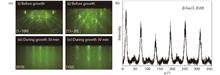
Monoclinic gallium oxide (Ga2O3) has been grown on (0001) sapphire (Al2O3) substrate by plasma-assisted molecular beam epitaxy (PA-MBE). The epitaxial relationship has been confirmed to be [010]( ) β-Ga2O3||[ ](0001)Al2O3 via in-situ reflection high energy electron diffraction (RHEED) monitoring and ex-situ X-ray diffraction (XRD) measurement. Crystalline quality is improved and surface becomes flatter with increasing growth temperature, with a best full width at half maximum (FWHM) of XRD ω-rocking curve of ( ) plane and root mean square (RMS) roughness of 0.68° and 2.04 nm for the sample grown at 730 °C, respectively. Room temperature cathodoluminescence measurement shows an emission at ~417 nm, which is most likely originated from recombination of donor–acceptor pair (DAP).
Jan. 01, 2019Vol. 40 Issue 1 012802 (2019)
Yuanjie Lü, Xubo Song, Zezhao He, Yuangang Wang, Xin Tan, Shixiong Liang, Cui Wei, Xingye Zhou, and Zhihong Feng
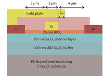
Ga2O3 metal–oxide–semiconductor field-effect transistors (MOSFETs) with high-breakdown characteristics were fabricated on a homoepitaxial n-typed β-Ga2O3 film, which was grown by metal organic chemical vapor deposition (MOCVD) on an Fe-doped semi-insulating (010) Ga2O3 substrate. The structure consisted of a 400 nm unintentionally doped (UID) Ga2O3 buffer layer and an 80 nm Si-doped channel layer. A high k HfO2 gate dielectric film formed by atomic layer deposition was employed to reduce the gate leakage. Moreover, a source-connected field plate was introduced to enhance the breakdown characteristics. The drain saturation current density of the fabricated device reached 101 mA/mm at Vgs of 3 V. The off-state current was as low as 7.1 × 10⁻¹¹ A/mm, and the drain current ION/IOFF ratio reached 109. The transistors exhibited three-terminal off-state breakdown voltages of 450 and 550 V, corresponding to gate-to-drain spacing of 4 and 8 μm, respectively.
Jan. 01, 2019Vol. 40 Issue 1 012803 (2019)
Tongchuan Ma, Xuanhu Chen, Fangfang Ren, Shunming Zhu, Shulin Gu, Rong Zhang, Youdou Zheng, and Jiandong Ye
The 8 μm thick single-crystalline α-Ga2O3 epilayers have been heteroepitaxially grown on sapphire (0001) substrates via mist chemical vapor deposition technique. High resolution X-ray diffraction measurements show that the full-widths-at-half-maximum (FWHM) of rocking curves for the (0006) and (10-14) planes are 0.024° and 0.24°, and the corresponding densities of screw and edge dislocations are 2.24 × 10⁶ and 1.63 × 109 cm-2, respectively, indicative of high single crystallinity. The out-of-plane and in-plane epitaxial relationships are [0001] α-Ga2O3//[0001] α-Al2O3 and [11-20] α-Ga2O3//[11-20] α-Al2O3, respectively. The lateral domain size is in micron scale and the indirect bandgap is determined as 5.03 eV by transmittance spectra. Raman measurement indicates that the lattice-mismatch induced compressive residual strain cannot be ruled out despite the large thickness of the α-Ga2O3 epilayer. The achieved high quality α-Ga2O3 may provide an alternative material platform for developing high performance power devices and solar-blind photodetectors.
Jan. 01, 2019Vol. 40 Issue 1 012804 (2019)
Jianjun Shi, Xiaochuan Xia, Qasim Abbas, Jun Liu, Heqiu Zhang, Yang Liu, and Hongwei Liang
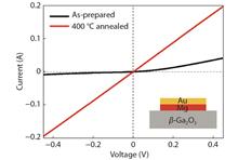
The carrier transport mechanism of Mg/Au ohmic contact for lightly doped β-Ga2O3 is investigated. An excellent ohmic contact has been achieved when the sample was annealed at 400 °C and the specific contact resistance is 4.3 × 10⁻⁴ Ω·cm2. For the annealed sample, the temperature dependence of specific contact resistance is studied in the range from 300 to 375 K. The specific contact resistance is decreased from 4.3 × 10⁻⁴ to 1.59 × 10⁻⁴ Ω·cm2 with an increase of test temperature. As combination with the judge of E00, the basic mechanism of current transport is dominant by thermionic emission theory. The effective barrier height between Mg/Au and β-Ga2O3 is evaluated to be 0.1 eV for annealed sample by fitting experimental data with thermionic emission model.
Jan. 01, 2019Vol. 40 Issue 1 012805 (2019)
Hui Hao, Xiao Chen, Zhengcheng Li, Yang Shen, Hu Wang, Yanfei Zhao, Rong Huang, Tong Liu, Jian Liang, Yuxin An, Qing Peng, and Sunan Ding
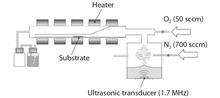
High quality gallium oxide (Ga2O3) thin films are deposited by remote plasma-enhanced atomic layer deposition (RPEALD) with trimethylgallium (TMG) and oxygen plasma as precursors. By introducing in-situ NH3 plasma pretreatment on the substrates, the deposition rate of Ga2O3 films on Si and GaN are remarkably enhanced, reached to 0.53 and 0.46 Å/cycle at 250 °C, respectively. The increasing of deposition rate is attributed to more hydroxyls (–OH) generated on the substrate surfaces after NH3 pretreatment, which has no effect on the stoichiometry and surface morphology of the oxide films, but only modifies the surface states of substrates by enhancing reactive site density. Ga2O3 film deposited on GaN wafer is crystallized at 250 °C, with an epitaxial interface between Ga2O3 and GaN clearly observed. This is potentially very important for reducing the interface state density through high quality passivation.
Jan. 01, 2019Vol. 40 Issue 1 012806 (2019)

Yue Hao
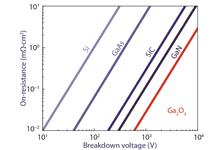
Despite being the long-time mainstream semiconductor for both logic and power devices, Silicon is now facing its dilemma and limitation of scalability and material potential. Especially for power devices, people are demanding escalating efficiency with higher blocking voltage while its power consumption and heat generation are less. Constrained by its narrow bandgap of 1.14 eV, Silicon only has a critical breakdown field (Ec) of 0.3 MV/cm, yielding a Baliga figure-of-merit (BFOM = ε × μ × Ec3) of unity when normalized to itself. It is hence required that the dominating factor Ec should be as high as possible such that the BFOM will be hundreds or even thousands of times when compared to Silicon so as to minimize the conduction loss. Beta-Gallium Oxide (β-Ga2O3) with decent μ of 250 cm2/Vs, ultra-wide bandgap of 4.8 eV and high critical Ec of 8 MV/cm, yielding a superior high BFOM of more than 3000. Therefore, system made with β-Ga2O3 can be thinner, lighter and capable of handling more power than the one with Silicon. In addition, low-cost and large size substrate through melt-grown method endows β-Ga2O3 more potentials as cost-effective power devices. After resolving the low thermal conductivity issue, unipolar devices made with ultra-wide bandgap β-Ga2O3 are promised to make power transition and our life more efficient.
Jan. 01, 2019Vol. 40 Issue 1 010301 (2019)
Xutang Tao, Jiandong Ye, Shibing Long, and Zhitai Jia
Jan. 01, 2019Vol. 40 Issue 1 010101 (2019)
Xutang Tao
Abstract
Jan. 01, 2019Vol. 40 Issue 1 010401 (2019)
H. F. Mohamed, Changtai Xia, Qinglin Sai, Huiyuan Cui, Mingyan Pan, and Hongji Qi
The rapid development of bulk β-Ga2O3 crystals has attracted much attention to their use as ultra-wide bandgap materials for next-generation power devices owing to its large bandgap (~ 4.9 eV) and large breakdown electric field of about 8 MV/cm. Low cost and high quality of large β-Ga2O3 single-crystal substrates can be attained by melting growth techniques widely used in the industry. In this paper, we first present an overview of the properties of β-Ga2O3 crystals in bulk form. We then describe the various methods for producing bulk β-Ga2O3 crystals and their applications. Finally, we will present a future perspective of the research in the area in the area of single crystal growth.
Jan. 01, 2019Vol. 40 Issue 1 011801 (2019)
Hang Dong, Huiwen Xue, Qiming He, Yuan Qin, Guangzhong Jian, Shibing Long, and Ming Liu
As a promising ultra-wide bandgap semiconductor, gallium oxide (Ga2O3) has attracted increasing attention in recent years. The high theoretical breakdown electrical field (8 MV/cm), ultra-wide bandgap (~ 4.8 eV) and large Baliga’s figure of merit (BFOM) of Ga2O3 make it a potential candidate material for next generation high-power electronics, including diode and field effect transistor (FET). In this paper, we introduce the basic physical properties of Ga2O3 single crystal, and review the recent research process of Ga2O3 based field effect transistors. Furthermore, various structures of FETs have been summarized and compared, and the potential of Ga2O3 is preliminary revealed. Finally, the prospect of the Ga2O3 based FET for power electronics application is analyzed.
Jan. 01, 2019Vol. 40 Issue 1 011802 (2019)
Hong Zhou, Jincheng Zhang, Chunfu Zhang, Qian Feng, Shenglei Zhao, Peijun Ma, and Yue Hao
Until very recently, gallium oxide (Ga2O3) has aroused more and more interests in the area of power electronics due to its ultra-wide bandgap of 4.5–4.8 eV, estimated critical field of 8 MV/cm and decent intrinsic electron mobility limit of 250 cm2/(V·s), yielding a high Baliga’s figures-of-merit (FOM) of more than 3000, which is several times higher than GaN and SiC. In addition to its excellent material properties, potential low-cost and large size substrate through melt-grown methodology also endows β-Ga2O3 more potential for future low-cost power devices. This article focuses on reviewing the most recent advances of β-Ga2O3 based power devices. It will be starting with a brief introduction to the material properties of β-Ga2O3 and then the growth techniques of its native substrate, followed by the thin film epitaxial growth. The performance of state-of-art β-Ga2O3 devices, including diodes and FETs are fully discussed and compared. Finally, potential solutions to the challenges of β-Ga2O3 are also discussed and explored.
Jan. 01, 2019Vol. 40 Issue 1 011803 (2019)
Bo Fu, Zhitai Jia, Wenxiang Mu, Yanru Yin, Jian Zhang, and Xutang Tao
As a wide-bandgap semiconductor (WBG), β-Ga2O3 is expected to be applied to power electronics and solar blind UV photodetectors. In this review, defects in β-Ga2O3 single crystals were summarized, including dislocations, voids, twin, and small defects. Their effects on device performance were discussed. Dislocations and their surrounding regions can act as paths for the leakage current of SBD in single crystals. However, not all voids lead to leakage current. There’s no strong evidence yet to show small defects affect the electrical properties. Doping impurity was definitely irrelated to the leakage current. Finally, the formation mechanism of the defects was analyzed. Most small defects were induced by mechanical damages. The screw dislocation originated from a subgrain boundary. The edge dislocation lying on a plane slightly tilted towards the (102) plane, the (101) being the possible slip plane. The voids defects like hollow nanopipes, PNPs, NSGs and line-shaped grooves may be caused by the condensation of excess oxygen vacancies, penetration of tiny bubbles or local meltback. The nucleation of twin lamellae occurred at the initial stage of " shoulder part” during the crystal growth. These results are helpful in controlling the occurrence of crystal defects and improving the device performance.
Jan. 01, 2019Vol. 40 Issue 1 011804 (2019)
Xiangqian Xiu, Liying Zhang, Yuewen Li, Zening Xiong, Rong Zhang, and Youdou Zheng
Halide vapor phase epitaxy (HVPE) is widely used in the semiconductor industry for the growth of Si, GaAs, GaN, etc. HVPE is a non-organic chemical vapor deposition (CVD) technique, characterized by high quality growth of epitaxial layers with fast growth rate, which is versatile for the fabrication of both substrates and devices with wide applications. In this paper, we review the usage of HVPE for the growth and device applications of Ga2O3, with detailed discussions on a variety of technological aspects of HVPE. It is concluded that HVPE is a promising candidate for the epitaxy of large-area Ga2O3 substrates and for the fabrication of high power β-Ga2O3 devices.
Jan. 01, 2019Vol. 40 Issue 1 011805 (2019)
© Copyright 2018-2021 | Chinese Laser Press.
All Rights Reserved 沪ICP备15018463号-20