


 View fulltext
Junchuan Liang, Yi Hu, Liming Ding, and Zhong Jin
Jan. 01, 1900Vol. 45 Issue 3 030201 (2024)
Wenbo Qiu, Zidong Wang, Shijiang He, Huaping Zhao, and Yong Lei
Jan. 01, 1900Vol. 45 Issue 3 030202 (2024)
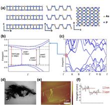
Chao Shen, Wenkang Zhan, Manyang Li, Zhenyu Sun, Jian Tang, Zhaofeng Wu, Chi Xu, Bo Xu, Chao Zhao, and Zhanguo Wang
Ex situ characterization techniques in molecular beam epitaxy (MBE) have inherent limitations, such as being prone to sample contamination and unstable surfaces during sample transfer from the MBE chamber. In recent years, the need for improved accuracy and reliability in measurement has driven the increasing adoption of in situ characterization techniques. These techniques, such as reflection high-energy electron diffraction, scanning tunneling microscopy, and X-ray photoelectron spectroscopy, allow direct observation of film growth processes in real time without exposing the sample to air, hence offering insights into the growth mechanisms of epitaxial films with controlled properties. By combining multiple in situ characterization techniques with MBE, researchers can better understand film growth processes, realizing novel materials with customized properties and extensive applications. This review aims to overview the benefits and achievements of in situ characterization techniques in MBE and their applications for material science research. In addition, through further analysis of these techniques regarding their challenges and potential solutions, particularly highlighting the assistance of machine learning to correlate in situ characterization with other material information, we hope to provide a guideline for future efforts in the development of novel monitoring and control schemes for MBE growth processes with improved material properties.
Jan. 01, 1900Vol. 45 Issue 3 031301 (2024)

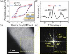
Shuyu Wu, Rongrong Cao, Hao Jiang, Yu Li, Xumeng Zhang, Yang Yang, Yan Wang, Yingfen Wei, and Qi Liu
The performance and reliability of ferroelectric thin films at temperatures around a few Kelvin are critical for their application in cryo-electronics. In this work, TiN/Hf0.5Zr0.5O2/TiN capacitors that are free from the wake-up effect are investigated systematically from room temperature (300 K) to cryogenic temperature (30 K). We observe a consistent decrease in permittivity (εr) and a progressive increase in coercive electric field (Ec) as temperatures decrease. Our investigation reveals exceptional stability in the double remnant polarization (2Pr) of our ferroelectric thin films across a wide temperature range. Specifically, at 30 K, a 2Pr of 36 μC/cm2 under an applied electric field of 3.0 MV/cm is achieved. Moreover, we observed a reduced fatigue effect at 30 K in comparison to 300 K. The stable ferroelectric properties and endurance characteristics demonstrate the feasibility of utilizing HfO2 based ferroelectric thin films for cryo-electronics applications.
Jan. 01, 1900Vol. 45 Issue 3 032301 (2024)
Zhenwu Liu, Li Zhong, Suping Liu, and Xiaoyu Ma
The 975 nm multimode diode lasers with high-order surface Bragg diffraction gratings have been simulated and calculated using the 2D finite difference time domain (FDTD) algorithm and the scattering matrix method (SMM). The periods and etch depth of the grating parameters have been optimized. A board area laser diode (BA-LD) with high-order diffraction gratings has been designed and fabricated. At output powers up to 10.5 W, the measured spectral width of full width at half maximum (FWHM) is less than 0.5 nm. The results demonstrate that the designed high-order surface gratings can effectively narrow the spectral width of multimode semiconductor lasers at high output power.
Jan. 01, 1900Vol. 45 Issue 3 032401 (2024)
Nicolò Zagni, Manuel Fregolent, Andrea Del Fiol, Davide Favero, Francesco Bergamin, Giovanni Verzellesi, Carlo De Santi, Gaudenzio Meneghesso, Enrico Zanoni, Christian Huber, Matteo Meneghini, and Paolo Pavan
Vertical GaN power MOSFET is a novel technology that offers great potential for power switching applications. Being still in an early development phase, vertical GaN devices are yet to be fully optimized and require careful studies to foster their development. In this work, we report on the physical insights into device performance improvements obtained during the development of vertical GaN-on-Si trench MOSFETs (TMOS’s) provided by TCAD simulations, enhancing the dependability of the adopted process optimization approaches. Specifically, two different TMOS devices are compared in terms of transfer-curve hysteresis (H) and subthreshold slope (SS), showing a ≈ 75% H reduction along with a ≈ 30% SS decrease. Simulations allow attributing the achieved improvements to a decrease in the border and interface traps, respectively. A sensitivity analysis is also carried out, allowing to quantify the additional trap density reduction required to minimize both figures of merit.
Jan. 01, 1900Vol. 45 Issue 3 032501 (2024)

Chao Feng, Xinyue Dai, Qimeng Jiang, Sen Huang, Jie Fan, Xinhua Wang, and Xinyu Liu
In this work, a novel one-time-programmable memory unit based on a Schottky-type p-GaN diode is proposed. During the programming process, the junction switches from a high-resistance state to a low-resistance state through Schottky junction breakdown, and the state is permanently preserved. The memory unit features a current ratio of more than 103, a read voltage window of 6 V, a programming time of less than 10?4 s, a stability of more than 108 read cycles, and a lifetime of far more than 10 years. Besides, the fabrication of the device is fully compatible with commercial Si-based GaN process platforms, which is of great significance for the realization of low-cost read-only memory in all-GaN integration.
Jan. 01, 1900Vol. 45 Issue 3 032502 (2024)
Jin Sui, Jiaxiang Chen, Haolan Qu, Yu Zhang, Xing Lu, and Xinbo Zou
Emission and capture characteristics of a deep hole trap (H1) in n-GaN Schottky barrier diodes (SBDs) have been investigated by optical deep level transient spectroscopy (ODLTS). Activation energy (Eemi) and capture cross-section (σp) of H1 are determined to be 0.75 eV and 4.67 × 10?15 cm2, respectively. Distribution of apparent trap concentration in space charge region is demonstrated. Temperature-enhanced emission process is revealed by decrease of emission time constant. Electric-field-boosted trap emission kinetics are analyzed by the Poole?Frenkel emission (PFE) model. In addition, H1 shows point defect capture properties and temperature-enhanced capture kinetics. Taking both hole capture and emission processes into account during laser beam incidence, H1 features a trap concentration of 2.67 × 1015 cm?3. The method and obtained results may facilitate understanding of minority carrier trap properties in wide bandgap semiconductor material and can be applied for device reliability assessment.
Jan. 01, 1900Vol. 45 Issue 3 032503 (2024)
Yong Sun, Wei Zhang, Shuang Han, Ran An, Xin-Sheng Tang, Xin-Lei Yu, Xiu-Juan Miao, Xin-Jun Ma, Xianglian, Pei-Fang Li, Cui-Lan Zhao, Zhao-Hua Ding, and Jing-Lin Xiao
Excitons have significant impacts on the properties of semiconductors. They exhibit significantly different properties when a direct semiconductor turns in to an indirect one by doping. Huybrecht variational method is also found to influence the study of exciton ground state energy and ground state binding energy in AlxGa1?xAs semiconductor spherical quantum dots. The AlxGa1?xAs is considered to be a direct semiconductor at Al concentration below 0.45, and an indirect one at the concentration above 0.45. With regards to the former, the ground state binding energy increases and decreases with Al concentration and eigenfrequency, respectively; however, while the ground state energy increases with Al concentration, it is marginally influenced by eigenfrequency. On the other hand, considering the latter, while the ground state binding energy increases with Al concentration, it decreases with eigenfrequency; nevertheless, the ground state energy increases both with Al concentration and eigenfrequency. Hence, for the better practical performance of the semiconductors, the properties of the excitons are suggested to vary by adjusting Al concentration and eigenfrequency
Jan. 01, 1900Vol. 45 Issue 3 032701 (2024)
Tingting Shi, Yuanbin Fan, Zhengyu Yan, Lai Zhou, Yang Ji, and Zhiliang Yuan
We demonstrate the photon-number resolution (PNR) capability of a 1.25 GHz gated InGaAs single-photon avalanche photodiode (APD) that is equipped with a simple, low-distortion ultra-narrowband interference circuit for the rejection of its background capacitive response. Through discriminating the avalanche current amplitude, we are able to resolve up to four detected photons in a single detection gate with a detection efficiency as high as 45%. The PNR capability is limited by the avalanche current saturation, and can be increased to five photons at a lower detection efficiency of 34%. The PNR capability, combined with high efficiency and low noise, will find applications in quantum information processing technique based on photonic qubits.
Jan. 01, 1900Vol. 45 Issue 3 032702 (2024)
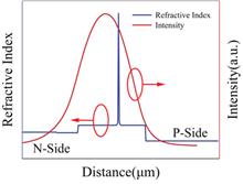
Xinfa Zhu, Weishuai Duan, Xiancheng Meng, Xiyu Jia, Yonghui Zhang, Pengyu Zhou, Mengjun Wang, Hongxing Zheng, and Chao Fan
The emergent two-dimensional (2D) material, tin diselenide (SnSe2), has garnered significant consideration for its potential in image capturing systems, optical communication, and optoelectronic memory. Nevertheless, SnSe2-based photodetection faces obstacles, including slow response speed and low normalized detectivity. In this work, photodetectors based on SnS/SnSe2 and SnSe/SnSe2 p?n heterostructures have been implemented through a polydimethylsiloxane (PDMS)?assisted transfer method. These photodetectors demonstrate broad-spectrum photoresponse within the 405 to 850 nm wavelength range. The photodetector based on the SnS/SnSe2 heterostructure exhibits a significant responsivity of 4.99 × 10³ A?W?1, normalized detectivity of 5.80 × 1012 cm?Hz1/2?W?1, and fast response time of 3.13 ms, respectively, owing to the built-in electric field. Meanwhile, the highest values of responsivity, normalized detectivity, and response time for the photodetector based on the SnSe/SnSe2 heterostructure are 5.91 × 10³ A?W?1, 7.03 × 1012 cm?Hz1/2?W?1, and 4.74 ms, respectively. And their photodetection performances transcend those of photodetectors based on individual SnSe2, SnS, SnSe, and other commonly used 2D materials. Our work has demonstrated an effective strategy to improve the performance of SnSe2-based photodetectors and paves the way for their future commercialization.
Jan. 01, 1900Vol. 45 Issue 3 032703 (2024)
© Copyright 2018-2021 | Chinese Laser Press.
All Rights Reserved 沪ICP备15018463号-20