


 View fulltext

2024
Volume: 53 Issue 5
18 Article(s)

Boshu SUN, Chunlei SUN, Renjie TANG, Yiting WANG, and Lan LI
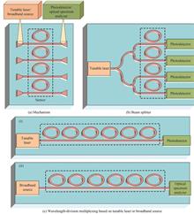
Sensors have been widely applied in various fields, such as environmental monitoring, biomedical engineering, and food safety. However, in recent years, there has been a growing demand for miniaturized sensing equipment or systems that can be used in portable or wearable applications. These application scenarios have imposed new requirements on sensing device size, weight, power consumption, and integration levels. Highly integrated sensing systems primarily rely on measuring changes in electrical or optical parameters. Compared with electrical sensors, optical sensors possess the advantages of immunity to external electromagnetic interference, stability, and label-free sensing capability. Fiber optic sensors are the most mature optical sensing method, known for their high sensitivity and low cost. However, they are constrained by their relatively large device size and the challenges associated with micro/nanofabrication, making it difficult to achieve high spatial density sensing arrays. Similarly, Surface Plasmon Resonance (SPR) sensors offer high sensitivity but require spatial optical coupling, resulting in a lower level of integration as sensing equipment. However, a compact integrated optical sensing device provides numerous benefits. It combines the advantages of optical sensing with low processing costs and high integration capabilities due to its compatibility with CMOS-compatible processes. Furthermore, by cascading multiple integrated photonic devices in an array, multi-site and multi-parameter sensing capability can be achieved with exceptional spatial resolution on a large scale, significantly enhancing the efficiency and functionality of the sensing system.Based on the method of light coupling to the optical sensors, the architecture for realizing multi-channel sensing arrays can be categorized into three types: mechanical scanning, spectroscopic scanning, and wavelength division multiplexing. Mechanical scanning approaches necessitate large dimensions of sensing systems and result in low operational efficiency. Spectroscopic methods reduce the optical power of single-channel sensing signals, with the number of channels limited by detector signal-to-noise ratio. Wavelength division multiplexing techniques exhibit high spectral utilization and are suitable for large-scale sensing applications, with the quality of sensing signals unaffected. However, sensing throughput is mainly limited by the tunable laser tuning range or the bandwidth of on-chip spectrometers.Integrated optical microcavities, typically smaller than conventional MZI and long waveguide structures, offer high-sensitivity responses due to their narrow line widths and could be cascaded for broadband operation, making them ideal for array sensing and enhancing sensing throughput. Optical microcavity structures serving as sensors mainly include micro-ring and micro-disk structures based on whispering gallery modes and defect and F-P type photonic crystal structures. Optical resonance peak shifts, splitting, and broadening of microcavities based on whispering gallery modes have been achieved in numerous studies of optical sensing at the single-molecule and single-particle levels. However, these studies rely on microcavity structures requiring three-dimensional fabrication techniques, making mass production challenging. Micro-disks can excite multiple modes, making it difficult to track resonance wavelengths. Micro-ring fabrication is relatively easier with high spectral utilization, making it the most commonly used integrated optical sensing unit. However, the periodicity of micro-ring spectra imposes limitations on the number of cascaded units that can be used, as the free spectral range constrains it. Defect photonic crystal structures are small in size with small mode volumes and low process tolerance, but the quality factor of unoptimized devices is limited. F-P type nanocavity microcavities are easier to fabricate but exhibit less optical field leakage and weaker interaction between light and matter, resulting in lower sensitivity. One-dimensional grating microcavity structures based on F-P cavities exhibit high sensitivity due to increased optical field leakage, but introduce more scattering losses due to additional sidewall roughness from fabrication, similarly limiting the quality factor. Although these three types of photonic crystal structures can achieve high throughput multi-channel cascading by coupling on the waveguide side, most devices perform worse than conventional micro-rings. Additionally, the high-precision micro/nano fabrication process required for these devices is beyond the capabilities of many foundries.While recent research has made significant progress in micro/nanofabrication and heterogeneous integration technologies, most efforts have focused on integrating sensing units with detection, leaving the research on fully integrated sensing systems relatively limited.Large-scale sensing arrays are now capable of mass production. However, challenges remain in realizing miniaturized high-throughput sensing systems and promoting industrial development, including insufficient scalability of sensing units, low integration of sensing systems, and a lack of mature packaging methods and testing processes. It is expected that in the future, more researchers will jointly promote the development of optical sensing systems through the optimization of optical structures and fabrication processes, drawing from existing large-scale system designs to improve performance, reduce dependence on high-precision, high-cost sensing unit design and fabrication, as well as reliable system packaging and testing processes.
May. 25, 2024Vol. 53 Issue 5 0553102 (2024)
Fei WANG, Yu BAI, Han BU, Chaoming NAN, Shize ZHANG, Yifan LI, Yanru ZHOU, Enbo XING, Lai LIU, Wenyao LIU, Ju TANG, and Jun LIU
At present, Resonant Optical Gyroscope (ROG) is developed towards integration, miniaturization, low power, and high resolution. However, the rotation signal of ROG is weak, and easily affected by reciprocal and nonreciprocal noises within the gyro system. With the growth of technical studies in ROG in recent years, the performance of ROG has been significantly improved. The improvement of noise suppression techniques and the combinations of multiple techniques in singe ROG system played important role in the measurement of a high signal-to-noise ratio and high precision rotation signal. With the aim of integration or miniaturization ROGs, noise suppression techniques also need to be further developed.So far, more studies on noise suppression focused on the suppression of nonreciprocal noises, which have different or inverse influences in the two counter propagating lights in the ROG system. The main part of nonreciprocal noises is backscattering noise. For the suppression of this kind of noise, a review of current studies is performed. More studies using the improved modulation techniques for noise suppression, which separate the sidebands in frequency domain in different ways. The separated frequencies cause lower interferences of the backscattering light or the influence can be filtered in the subsequent signal processing steps. However, the residual intensity modulation induced error appears as the modulation difference of the two loops. The error must be eliminated by improved demodulation designs. Another approach for backscattering noise suppression is using of multiple light sources. In this technique, Optical Phase-Locked Loop (OPLL) is used to lock the lasers in stable frequency difference, resulting in low coherence and interference.The second strength part of nonreciprocal noises is Kerr noise. The techniques of Kerr noise suppression are also reviewed. The main idea of these techniques is laser intensity monitoring. Realization of laser intensity monitoring used in ROGs is usually based on the secondary harmonic demodulation of the detected phase modulated laser signals. Theoretical and experimental studies have been carried out on the linear relation of the signal and laser intensity. As for intensity stabilization, there must be intensity modulators in ROGs to control the laser intensity according to the feedback of intensity related demodulation signals, which introduce more optical devices. Therefore, the studies for simplified intensity feedback loop are also performed, which use fewer modulators or directly compensate the induced error in the gyro output.A less effective part of the nonreciprocal noises is polarization fluctuation noise. The previous studies of this kind of noise are also presented. At present, the widely used polarization maintain fiber and polarizers in ROGs make the suppression of polarization fluctuation noise easier and more effective. However, for the use of WRR in the integrated ROGs, the resonators usually do not have the polarization maintain property inside, which remains a better solution requirement.As for the reciprocal noises in ROGs, with the intended reciprocal design of ROG and the nonreciprocal property of Sagnac effect, more important noise source lies inside the ROG system, namely the frequency and intensity noises of the light source. For the frequency noise suppression, more advanced laser frequency locking techniques can be performed. The presented reports introduce more laser frequency locking loops to improve the locking precision, which also improved the zero-bias stability of ROGs. Another approach for frequency stabilization is the use of OPLL, which works well in multi-laser ROG system. The self-injection locking technique in the laser side is also presented as an approach in frequency stabilization. The technique features a whole optical loop in the phase locking loop but precision improvement is still needed. The other noise of laser intensity here is mainly for the output power fluctuation in frequency domain, which cause the relations in the ROG for rotation sensing not as perfect as theoretical designs. The suppression of this type of noise is more considered in the laser design.Finally, tendency of integration and miniaturization of ROGs is refocused. For this reason, the ROG design must be reexamined. 1) Miniaturization of suppression systems. Miniaturization of optical devices makes lower signal-to-noise ratio as less robust against noise interferences. Besides, the adding of optical devices for noise suppression is also limited, which limit the realization of some noise suppression techniques. The more advanced optical designs and new techniques for multiply noise suppression in simple design are needed in the future. For example, the use of integrated optics design and the realization of integrated resonant cavities. 2) Fast response of noise suppression processing. More suppression techniques and feedback loops in use requires more complex signal processing and control algorithms. Powerful and simplification of design such as efficiently use of FPGA is also important in the future for fast processing. 3) Intelligent noise suppression technology. With the complexity of gyro systems, it is difficult to comprehensively analyze the ROG error analysis mechanism and construct error models, Intelligent algorithms are needed to help achieve this goal, such as the nonlinear suppression method based on cubature Kalman Filter-Phase Space Reconstruction (CKF-PSR) and the improved Variational Mode Decomposition (VMD) method. 4) Novelization of noise suppression mechanisms. New mechanisms and novel sensing structures should be presented, such as the use of broadband light sources, so that the coherence length of laser as well as backscattered light is shortened and good suppression can be achieved without adding additional optics. On the other hand, with the development of new types of optical gyro, new types of noises, such as optical power noise due to resonance tuning and gain fluctuations, and quantum noise, are constantly being derived, in spite of the consequent increase in the sensitivity and signal-to-noise ratio. Therefore, new mechanisms need to be developed to suppress these noises.
May. 25, 2024Vol. 53 Issue 5 0553103 (2024)
Xiaotian CHENG, Lingfang WANG, Jiawang YU, Shuning DING, Zhibo NI, Hongbin WANG, Xiaoqing ZHOU, and Chaoyuan JIN
The quantum theory of light reveals a counter-intuitive result for the existence of the lowest energy state of quantized light, the quantum vacuum state. According to quantum theory, the vacuum electromagnetic field that fills arbitrary spaces accounts for radiative transitions in condensed matter through carrier-photon interaction. With precisely designed nano-structures, it is possible to manipulate the local distribution of vacuum electromagnetic field in confined spaces. For instance, the Spontaneous Emission (SE) rate can be statically modified by shaping the vacuum field at the position of the nano-emitter when it is inside a micro-/nano-cavity or nearby a plasmonic structure. The typical experimental signature is either an inhibition or acceleration in SE rate.So far vacuum field and hence the SE rate at nano-scale is generally determined by the electromagnetic design. The enhancement or inhibition ratio of the SE rate is usually fixed after the device fabrication, while real-time(post-fabrication) manipulation of vacuum field brings in an additional tunability for Cavity Quantum Electrodynamics (CQED) studies. This paves the way for developing various applications in classical and quantum photonics that are otherwise impossible. Recently, dynamically tunable active devices based on semiconductor materials have been intensively investigated. This kind of dynamic or quasi-dynamic approach leads to a series of new nanophotonic device concepts and may find its applications in quantum light sources and micro-/nano-cavity lasers.This review focuses primarily on controlling radiative processes through post-fabrication manipulation of the vacuum electromagnetic field. Semiconductor optical microcavities, known for their ability to trap photons and prolong their lifetimes within the cavity, play a vital role in enhancing light-matter interactions by precisely manipulating the photon density of states, which are crucial for fundamental radiation processes such as spontaneous and stimulated emission.This review is organized as follows.: the first section outlines the fundamental theory of radiative processes within the framework of CQED, including detailed discussions on light-matter interactions and derivations of the local density of states and the Purcell factor for arbitrary inhomogeneous dielectrics. Efforts to minimize the mode volume of optical microcavity for an enhanced emission are discussed and further illustrated with a review on various micro- and nano-cavities including self-assembled quantum dots in photonic crystal (PhC) cavities. The second section focuses on SE in single or coupled cavities, especially within PhC cavities, summarizing three methods to dynamically manipulate the coupling effects of the emitter and devices to control their radiative processes. These include altering the refractive index distribution of semiconductor materials, dynamically controlling external environmental parameters of the emitters and micro-/nano-cavities, and real-time adjustment of coupling effects in these cavities. The review also details the implementation of cavity-emitter detuning variations in the PhC platform, enabling modulation of the SE rate of a quantum dot within a single photonic crystal cavity, and discusses manipulation of vacuum-field properties in two (or more) coupled cavities using external fields such as light, thermal, electrical, magnetic, and mechanical force fields. The last section discusses methods developed for controlling stimulated emission, emphasizing control methods involving field distribution in spatial pumping, coupled cavities, and complex physical mechanisms like parity-time symmetry.This review concludes with an outlook on future prospects of functional nanophotonic devices. We offer a brief outlook on future directions. The development of micro- / nano-photonic devices may focus on three areas: uncovering more complex physical mechanisms through innovative vacuum field control to enable advanced light-matter interactions; adopting more flexible control methods that allow independent manipulation of devices' temporal and spatial characteristics; and designing practical devices. These advancements are crucial for dynamically controlling device performance and integrating them into photonic chips and quantum information networks.
May. 25, 2024Vol. 53 Issue 5 0553104 (2024)
Jinlong ZHU, Hongbing FU, and Qing LIAO
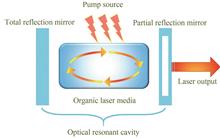
Since the invention of the first ruby laser in 1960, after more than 60 years of research and development, laser has been widely used in various industries due to its excellent characteristics such as high directionality, high brightness, and monochromaticity. Over the years, lasers have continuously evolved and innovated to meet market demands. While there are various laser shapes and pump sources available in the market, covering different output powers, wavelengths, and pulse durations, the core components of all lasers consist of the laser gain medium, pump source, and optical resonator cavity.Firstly, the conditions for the generation of organic lasers and the energy level system are introduced. Population inversion is crucial to overcome the competition between stimulated absorption and stimulated radiation. Achieving population inversion allows excited radiation to dominate, enhancing light intensity, which is the fundamental principle of laser amplification. However, in practice, not all luminescent materials can achieve the population inversion. To achieve the population inversion, a suitable energy level system is necessary. The four-level system is more effective in achieving population inversion compared to the three-level system.Next, the paper discusses organic semiconductor gain materials, which are the foundation of organic lasers. These materials enable population inversion and light amplification through stimulated emission. Organic semiconductor lasers stand out from others due to their use of organic materials as the laser gain medium. Compared with inorganic materials, organic materials offer high tunability in photoluminescence spectra, thanks to their abundant excited-state photophysical and photochemical processes. Additionally, the weak interaction between organic molecules allows for flexible control of crystal geometry and mass crystal fabrication. Meanwhile, the complex excited-state energy level system of organic materials is inherently more favourable for constructing a four-level system for the population inversion. The paper classifies luminescent mechanisms into fluorescent materials, thermally activated delayed fluorescent materials, and phosphorescent materials, summarizing the research progress in these areas.Finally, the paper focuses on optical resonant cavities, highlighting their two main functions: firstly, to generate and sustain laser oscillation by ensuring continuous stimulation of the gain medium through radiation, thereby achieving optical amplification. Secondly, to control the quality of the output laser beam by adjusting the geometric parameters of the resonant cavity, regulating the oscillation frequency, transverse distribution characteristics, and spot size of the laser beam. A well-designed resonant cavity can produce significant optical resonance in a small space for an extended period. Various types of optical resonant cavities have been developed based on different light-confining methods. The paper introduces the types of optical resonators and discusses the research progress in organic microcavity lasers based on various resonator structures, including planar waveguide and microcavity structures. Through the regulation of organic gain materials and the parameter modulation of the resonant cavity, not only enables the realization of full-wavelength lasers but also allows for customization of the frequency, transverse distribution characteristics, and mode selection of the laser output beam. The paper aims to serve as a reference for further exploration into organic microcavity lasers with innovative resonant cavity structures.
May. 25, 2024Vol. 53 Issue 5 0553105 (2024)
Chen CHEN, and Feng LIU
The quantum internet is a network that can transmit and store quantum information and connect multiple quantum processors. Such quantum networks are the basis of quantum information technologies such as quantum communication, distributed quantum computing, and quantum sensing. Due to photons having low environmental interaction and strong resistance to interference, mature optical fiber networks can provide a solid foundation for the transmission of optical quantum states, serving as an excellent carrier for long-distance transmission. Although the loss of photon transmission in optical fibers will limit the communication distance, the generated quantum state can still be successfully distributed to any remote destination through quantum repeaters.Solid-state sources that emit pairs of entangled photons are an important part of optical quantum networks. In the past, spontaneous parametric down conversion has been used in most photon-based entanglement experiments. However, the generation of photons in this way is a probabilistic process following Poisson statistics. Hence, the probability of generating multiple pairs of photons within an excitation cycle is non-zero, necessitating a balance between the source brightness and the multi-photon emission probability. This would limit applications in complex quantum protocols. Self-assembled semiconductor quantum dots are one of the primary candidates for the deterministic generation of entangled photon pairs, possessing excellent properties of high efficiency, high purity, high indistinguishability, and high entanglement fidelity. Moreover, it can be compatible with semiconductor micro-nano processing technology widely used in the industry and integrated into photonic chips. Among various systems suitable for quantum information research, quantum dots are one of the most attractive choices.However, establishing quantum relays based on quantum dot entangled photon sources still faces some challenges. On the one hand, due to the stochastic nature of quantum dot growth, different quantum dots exhibit variations in size, shape, and composition. It is difficult to find multiple quantum dots within the same quantum chip with identical biexciton or exciton energies, directly limiting the Bell state measurement and thereby preventing entanglement transmission between quantum network nodes via quantum interference. On the other hand, anisotropies in strain, shape, and composition reduce the symmetry of quantum dots, the electron-hole exchange interaction leads to fine-structure splitting between two bright exciton states. This causes the entanglement fidelity to exhibit oscillating behavior over the time span t between biexciton and exciton photon emission, resulting in lower long-term integrated entanglement fidelity in experimental measurements. When fine-structure splitting is present, a well-entangled photon source can be obtained through temporal post-selection. However, this will lose most of the entangled photon pairs and reduce the effective brightness of the source. Alternatively, using high-resolution single-photon detectors or external optical techniques to ‘compensate’ for the evolution characteristics of entangled states. Yet, these technical requirements diminish the appeal of quantum dots in scalable quantum technologies. The most direct and effective approach is the elimination of fine-structure splitting itself.In the past few decades, it has been confirmed that the post-growth tuning of quantum dots through thermal annealing, magnetic fields, lateral electric fields, vertical electric fields, optical fields, and strain fields successfully eliminates fine-structure splitting and generates entangled photon pairs. Despite the help of these tuning techniques, there is still a problem that the two factors of emission wavelength and fine-structure splitting cannot be tuned independently. When one factor is tuned to the target position, it often leads to the deviation of the other factor from its target value, making simultaneous improvements challenging. Wavelength-tunable entangled photon sources are a fundamental requirement for transmitting entanglement between quantum network nodes via quantum interference. This promotes the development of the field from single-degree-of-freedom tuning to multi-degree-of-freedom tuning. This multi-degree-of-freedom joint tuning paves the way for wavelength-tunable quantum dot entangled photon sources.In this article, the causes behind the non-uniform wavelength and fine-structure splitting in quantum dots are elucidated, providing an overview of recent years that use multi-degree-of-freedom tuning to achieve the tuning of both emission wavelength and fine-structure splitting. According to the different combined approaches, the combined tuning mechanisms are divided into four types: combined stress and electric field, combined magnetic field and electric field, anisotropic strain, combined light field and electric field. The tuning methods and current research status of these distinct mechanisms are reviewed. Finally, apart from the two important aspects of tunable emission wavelength and high entanglement fidelity, applying quantum dot entangled photon sources effectively in quantum relays necessitates enhancing the collection efficiency and indistinguishability of the entangled photon source. It is highlighted that these aspects could potentially be improved by coupling quantum dots into optical microcavities and using the Purcell effect, offering a perspective on the future development of wavelength-tunable quantum dot entangled photon sources.
May. 25, 2024Vol. 53 Issue 5 0553106 (2024)

Jiancheng LI, Binjuan LEI, Jinlong XIAO, Yuede YANG, and Yongzhen HUANG
Semiconductor chaotic lasers have been investigated for physical random bit generation, secure communication, and chaotic detection, owing to its characteristics of randomness, high sensitivity to initial conditions, and broad radio-frequency spectrum. In order to destabilize the semiconductor lasers for chaos generation, external perturbations are usually required, such as optical injection, optical feedback, or optoelectronic feedback. However, semiconductor chaotic laser systems consisting of discrete optical components are susceptible to environmental disturbance. Then, various integrated chaotic semiconductor lasers have been developed to meet the requirement of miniaturization and stability. A deterministic polarization chaos without external perturbation was also reported in Vertical-Cavity Surface-Emitting Laser (VCSELs). Whispering gallery microcavity has become an important optical platform for laser nonlinear researches because of its high quality-factor and small mode volume. Compared with integrated chaos chips and self-chaotic VCSELs, self-chaotic microcavity lasers with the small volume, large chaotic bandwidth and wide chaotic operation condition, require simple process without repeated epitaxy, and are easy to mass production with low cost. In this paper, we review the progress on chaotic microcavity lasers in three aspects: self-chaotic microlasers, chaotic microlasers based on optical feedbak, and integrated mutual-injection microlasers. We also introduce the applications of self-chaotic microcavity lasers.The progresses on the self-chaotic microcavity lasers without external perturbations are first reviewed. A circular-sided hexagonal chaotic microlasers was introduced due to the internal mode interaction of two transverse modes. When the mode interval is below the relaxation oscillation frequency, carrier density can oscillate dramatically with the mode-beating, and an internal optical-injection perturbation is obtained with side-peaks of lasing modes. Consequently, chaotic dynamics could spontaneously generate due to carrier oscillation at mode-beating frequency and the internal injection between the two lasing modes. Compared with hexagonal microcavity, the square microcavity has more obvious in-phase and anti-phase region. The spontaneous chaos is expected to be realized more easily in a square microcavity. Then, a circular-sided square microcavity self-chaotic laser with dual-transverse-mode is introduced. Pulse-packages phenomenon in a microcavity laser, induced by near-degenerate modes beating, was experimentally discovered for the first time. With the continuous increase of the current, the evolution route of period one, period three, and chaos state is first clearly experimentally illustrated in a microcavity laser. The importance of near-degenerate modes for chaos generation is revealed. The working current range of the chaotic state of the circular-sided square microcavity laser is not less than 10 mA, the maximum effective bandwidth is 22.4 GHz, and the flatness is ±4 dB. The performance of the microcavity chaotic laser is greatly improved, and the packaged chaotic lasers for practical applications have become a reality. To enhance the self-chaotic bandwidth of microcavity laser, the method by the on-chip photon-photon resonance effect was proposed. A three transverse-mode microcavity chaotic laser with enhanced chaotic bandwidth was introduced. Through the interaction of three transverse modes, a chaotic bandwidth of 33.9 GHz was obtained.Then, chaos microcavity lasers due to optical feedback are presented for dual-mode and tri-mode microcavity lasers. Two mode and tri-mode feedback are investigated for chaos generation and chaotic bandwidth enhancement. Chaos is easily generated by multi-mode optical feedback. And mode-beating in optical feedback can greatly improve the chaotic bandwidth. And the nonlinear dynamics caused by integrated mutual-injection microdisk and microring lasers are introduced in the third section.Finally, the applications of self-chaotic microcavity lasers are summarized. A physical random bit generator at 10 Gb/s based on the self-chaotic circular-sided hexagonal microcavity laser was first demonstrated. Then, the chaotic output of the three-mode self-chaotic circular-sided square microcavity is used as the entropy source for random number generation. Under the real-time sampling of 100 Gsa/s, the post-processsing methods including delay-difference and retaining five least significant bits are adopted. Physical random numbers at 500 Gb/s that pass the NIST SP 800-22 standard randomness tests are obtained. In addition, based on a microcavity chaotic laser with a double-peak structure in the temporal intensity distribution of chaotic signals, 400 Gb/s physical random numbers are realized by only retaining four least significant bits with 100 Gsa/s real-time sample. We also achieve 50 Gb/s physical random bits by directly extracting the chaotic microwave signal from the P-electrode of the deformed square self-chaotic microlaser. In addition, a chaotic correlation optical time-domain reflectometer is constructed based on a fabricated self-chaotic microcavity laser, in which a fiber detection distance of 25 km and a spatial resolution of 4.5 mm are demonstrated.The self-chaotic microcavity lasers pave the way of mode engineering for deformed microcavity lasers. A random number generator based on the self-chaos deformed square laser can simplify the system greatly due to a small footprint and low power consumption for the chaotic microlasers. Moreover, self-chaotic lasers have potential applications in secure communication, chaos radar, etc.
May. 25, 2024Vol. 53 Issue 5 0553107 (2024)
Jianfei LIU, Zhigang HU, Yimeng GAO, and Beibei LI
Sensors serve as an extension of human senses, facilitating the heightened perception and profound comprehension of the world. Among various kinds of sensors, magnetic field sensors play an increasingly vital role across diverse areas, such as biomedicine, aerospace, military, and industry, as well as fundamental scientific research. Currently, the state-of-the-art magnetic sensors are based on Superconducting Quantum Interference Devices (SQUIDs), with exceptional sensitivity at the fT/Hz1/2 level. However, their reliance on cryogenic systems leads to high operational costs and limited applications. In recent decades, significant advancements have been made in other magnetic sensors that can work at room temperature, including Hall sensors, optical atomic magnetometers, diamond Nitrogen Vacancy (NV) center magnetic sensors, etc. This review sheds light on an emerging, high-sensitivity magnetic field sensor known as the Optical Microcavity Magnetic sensor (OMM). OMMs utilizing high-quality factor optical microcavities have enabled precision sensing of magnetic fields, featuring high sensitivity, broad bandwidth, and low power consumption. In this review, we focus on recent advances using three types of OMMs: magnetostrictive magnetic sensors, torque magnetic sensors, and magneto-optic magnetic sensors. We provide an overview of the magnetic field sensing mechanisms employed by these three OMMs and survey the recent relevant progress. Furthermore, we discuss the sensitivity improvement methods through response enhancement and noise suppression. Finally, this review provides an outlook on the potential of OMMs for magnetic induction tomography and corona current monitoring.Based on their sensing mechanisms, OMMs can be typically categorized into magnetostrictive magnetic sensors, torque magnetic sensors, and magneto-optic magnetic sensors. The magnetostrictive magnetic sensors combine magnetostrictive materials with optical microcavities. The applied magnetic field induces strain within the magnetostrictive material, which can drive the mechanical motion of the microcavity, leading to a change in the radius of the microcavity. This radius change shifts the optical resonance, resulting in a periodic change in the intracavity field. Consequently, the magnetic field can be optically read out using the intensity-modulating mechanism, with sensitivity enhanced by the dual-resonance of optical and mechanical modes. Initially, researchers achieved OMMS by embedding magnetostrictive particles such as Tefernol-D into optical microcavities. The sensitivity has been improved by optimizing the geometric parameters and improving the overlap between the magnetostrictive material and the microcavity. In efforts to achieve scalable and stable magnetostrictive magnetic sensors, researchers have sputtered the magnetostrictive thin films onto the optical microcavity and even integrated it with a waveguide. Recently, sensitivities of 26 pT/Hz1/2 and 585 pT/Hz1/2 have been achieved by using the magnetostrictive materials of Terfenol-D particles and Terfenol-D thin films, respectively.Torque magnetic sensors consist of a torque mechanical resonator coated with a magnetic material layer and an optical microcavity such as a photonic crystal microcavity or an optical whispering gallery mode microcavity, with an air gap between the mechanical resonator and the optical cavity. The magnetic field exerts a moment on the torque, causing excitation of the torsional mode and altering the distance between the optical microcavity and the torque oscillator. This change in distance affects the effective refractive index of the optical mode, resulting in periodic shifts in the resonance frequency of the optical mode. Therefore, the magnetic field or the magnetic moment of the material can be optically read out using the intensity-modulating mechanism. Magneto-optic magnetic sensors involve injecting the magnetic fluid into microcavities such as capillary and Fabry-Perot fiber cavities. The magnetic nanoparticles within the magnetic fluid can form chain-like structures as a magnetic field is applied, resulting in a change in the refractive index of the magnetic fluid, which induces a shift in the optical resonance. Thus, the magnetic field can be read out by the variation of the optical transmission.Sensitivity is a critical parameter for magnetic sensors as it determines their ability to detect weak magnetic fields. In the case of magnetic-optic magnetic sensors, sensitivity is commonly evaluated by measuring the mode shift caused by a unit magnetic field, expressed in units of nm/mT. On the other hand, for optomechanical magnetic sensors like magnetostrictive magnetic sensors and torque magnetic sensors, sensitivity is typically characterized by the noise-equivalent magnetic field. This metric represents the amplitude of the magnetic field that the sensor can detect at a signal-to-noise ratio of 1, with a measurement resolution bandwidth of 1 Hz, measured in T/Hz1/2. The noise sources of optomechanical magnetic sensors consist of thermal noise from the nonzero-temperature bath, shot noise from the laser, and back action noise originating from the radiation pressure shot noise heating. The sensitivity of optomechanical magnetic sensors is minimal near the mechanical resonance frequency where thermal noise dominates, and degrades in the shot-noise-limited regime. In this review, we focus on the optomechanical magnetic sensors as an example to discuss the sensitivity improvement methods through signal enhancement and noise suppression. In the regime of response enhancement, sensitivity can be improved by selecting materials that exhibit higher sensitivity to the magnetic field and optimizing the structural design of the magnetic sensor. Additionally, the response to the magnetic field can be amplified by employing a flux concentrator which enhances the magnetic field signal. In the regime of noise suppression, the sensitivity can be improved by reducing the shot noise level of the laser using squeezed light or performing joint measurements with entangled light.While there is still progress to be made in improving the sensitivity, stability, and scalability of OMMs, their unique advantages make them a promising technology for future magnetic field sensing applications. Continued research and development efforts are expected to address the current challenges and unlock the full potential of OMMs in practical application scenarios, such as magnetic induction tomography and corona current detection.
May. 25, 2024Vol. 53 Issue 5 0553108 (2024)
Xiaochong YU, and Chenglong DAI
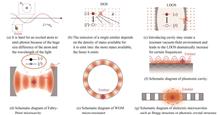
The ultra-high quality factor (typically above 107) of the whispering-gallery microresonators such as microsphere, microtoroid, microbubble is mainly due to the total-internal-reflection and ultra-smooth surface. Usually, higher quality factor corresponding to narrower linewidth and longer photon life-time, which strongly increase the light-matter interaction and sensing performance, makes those microresonators the perfect platform for the nonlinear optics and optical sensing research. To further optimize the quality factor, analysis and suppressing the main loss channels is needed. The loss in a whispering-gallery microresonator is mainly depends on absorption loss, scattering loss and radiation loss. Among them, the radiation loss of the resonator is more obvious for small cavity or lower refractive contrast, while the absorption loss and scattering loss from the bulk cavity material have less dependence with the cavity size. Since the fast development of fabrication techniques, the bulk absorption and scattering loss can be strongly suppressed, while the surface scattering loss trends to become dominant for large cavities. However, the previous estimations of surface scattering have a range covers several orders of magnitude, which also become unacceptable for meeting the requirement of further improvement.In this article, the surface scattering loss of a spherical microcavity with the tiny random surface roughness (far below the optical wavelength) is analyzed by applying the equivalent current method. The surface function of the microcavity is first transfer to the equivalent polarization current which excite the secondary modes. By combining the simplified total radiation power of the excited modes with the estimation of the surface field component, a more precise estimation of surface scattering loss is finally provided and further verified via numerical calculation.In detail, this equivalent current can be expressed as the superposition of two tangential fields and one radial field on surface of the microsphere. Among them, the transverse electric (TE) modes can only be excited by the tangential current, while the transvers magnetic (TM) modes can be excited by both the tangential and radial currents. Here, for simplicity, the equivalent current expansion for four TE modes is calculated because they only have the tangential part, and the scattering power can thus be calculated by adding together all the radiation power of the excited TE and TM radiation modes, and the total scattering power from the modes with same angular momentum is proportional to the angular momentum. Note that, for the TE radiation modes, the current expansion coefficient is proportional to the field overlapping of the original TE mode, and the scattering field is similar to the radiation field of the original TE mode.The total scattering cross-section of the random surface is similar to a collection of dipole scatterers NVp2/λ4=R2σ2B2/λ4, where N is the number of scatters, Vp is the Root Mean Square (RMS) volume of the scatterers, λ is the resonance wavelength, R is the cavity radius, σ2 and B is the variance and the correlation length of the surface function. Thus, the scattering quality factor shows a dependence of λ3R/σ2B2, This result agrees with the estimation given by GORODETSKY M L, and its two-dimension version λ2R/σ2B agrees with the perturbation theory developed by WIERSIG J. To verify this result, by applying the equivalent parameter, numerical simulation of the scattering power for the random sampling of surface point-like scatterers is demonstrated, and the surface current and the total scattering power agree well with the theory.This method can directly apply to TM modes by further consider the TM radiation mode excited by the radial part of the equivalent current. If the resonance modes have other loss channels such as a pillar in the real case, the low quality factor resonance modes should also be considered, and the scattering quality factor is further decreased. For longer correlation length, the equivalent current could introduce stronger coupling between modes, and also influence the scattering power.
May. 25, 2024Vol. 53 Issue 5 0553109 (2024)
Wenhao LI, Pinggang JIA, Jun WANG, Bo XUE, Shun WAN, Kaiyao HOU, and Jijun XIONG
Micro pressure sensors play a crucial role in pressure measurement in narrow spaces, especially in the medical field. Traditional pressure sensors are limited in small space applications due to their large size. The advantages of miniaturized pressure sensors are highlighted. The measurement of pressure within the organism during clinical diagnosis and minimally invasive surgery can provide doctors with necessary diagnostic information, decision support, and guidance for treatment. Real time monitoring of internal pressure is a key factor in determining the success or failure of treatment, especially in cardiovascular surgery, head injury recovery, and urological intervention. With the development of Micro Electro Mechanical Systems(MEMS) technology and the improvement of medical standards, various types of miniaturized pressure sensors have begun to enter the field of biology, including electronic pressure sensors and fiber optic sensors. Electronic sensors, including piezoelectric, resistive, and capacitive pressure sensors, have complex structures and are not resistant to electromagnetic interference, which limits their applications in the medical field. Compared with traditional electronic sensors, fiber optic sensors have received widespread attention due to their small size, simple structure, high sensitivity, corrosion resistance, and resistance to electromagnetic interference. At present, most of the reported fiber optic sensors are based on fiber Bragg grating and Fabry Perot. The core component of fiber optic Fabry Perot sensors is the Fabry Perot cavity, and its preparation process is mainly divided into manual single preparation and MEMS technology batch preparation. Single prepared sensors are produced in one go, with poor consistency and difficulty in mass production. By contrast, the MEMS technology can not only improve sensor consistency but also reduce costs to achieve large-scale production. A micro fiber optic Fabry Perot sensor based on MEMS technology is designed and prepare. The sensor has the characteristics of high sensitivity and batch manufacturing. Based on the research of biocompatible materials, Silicon-On-Insulator(SOI) and BF33 glass were selected as sensor sensitive materials on insulating substrates. The etched SOI device layer is made of monocrystalline silicon as a sensitive membrane, and the etching depth is used as the initial cavity length of the micro Fabry Perot cavity. It is then bonded together with BF33 glass through anodic bonding technology to form a vacuum sealed micro Fabry Perot cavity array on the bonding surface. Monocrystalline silicon and BF33 glass form two reflective surfaces in a miniature Fabry Perot cavity. The incident light enters the cavity and undergoes double beam interference. When the external pressure changes, the sensitive membrane deforms, resulting in a change in the length of the Fabry Perot cavity. The signal is transmitted to the demodulation system through optical fibers to determine the change in external pressure. By using femtosecond laser fine cutting technology to independently separate the sensor unit, and using a micro displacement platform under a microscope to integrate the fiber and sensor head, the overall outer diameter and the high of a single sensor is only 400 μm and 220 μm, respectively. We built a signal demodulation experimental platform and conducted detailed tests on the pressure characteristics of the sensor. The test results show that within the gas pressure range of 0~50 kPa, the pressure sensitivity of the sensor can reach 18.5 nm/kPa, with a maximum nonlinearity of 0.47%, a repeatability of 0.18%, a hysteresis of 0.18%, and a small cross sensitivity coefficient within the range of human temperature changes. In summary, the sensor designed and prepared in this paper with advantages such as small size, high sensitivity, electromagnetic compatibility, biocompatibility, and strong stability, provide enormous commercial conversion value in the fields of biomedical and medical science.
May. 25, 2024Vol. 53 Issue 5 0553110 (2024)
Xin SUN, Wenxiu LI, Shuo JIANG, Zongqi YANG, Xinyao HUANG, Hao ZHANG, Anping HUANG, and Zhisong XIAO
To precisely control the transmission spectra of micro-ring resonators, a design incorporating arrays of etched air holes was introduced into the micro-ring resonator and coupled waveguide system. Modeling was completed using deep learning algorithms and inverse design techniques to predict the forward transmission spectra and optimize the performance of Fano resonance spectrum through inverse design. Based on the inverse design results, the slope of the transmission spectra was nearly doubled after 12 iterations of enhancement.For the preparation of the dataset, a system consisting of a single micro-ring resonator coupled with a straight waveguide was investigated. Six rows by six columns of air holes, each with a diameter of 100 nm, were introduced at both ends. Light enters the micro-ring resonator from the left design area and passes through to the right design area. The etched air hole arrays in these areas affect the propagation of light. Based on this micro-ring waveguide system, 5 000 samples were obtained using Finite-Difference Time-Domain (FDTD) simulations. These samples included the distribution of air hole arrays at both ends of the coupled waveguide and the corresponding micro-ring transmission spectra data. Utilizing the deep learning multi-layer perceptron algorithm, modeling was performed with the structure of the air hole arrays as input and the transmission spectra as output. This successfully enabled the prediction of micro-ring transmission output spectra within 24 ms for different air hole etchings. The cosine similarity values between the predicted spectra and traditional simulation spectra were close to 1.0.Next, an asymmetry index was defined and combined with the number of resonance peaks to distinguish between Fano and non-Fano line shapes in the dataset. To establish an inverse design model, the slope was defined as a performance indicator for the Fano resonance line shape in micro-ring resonators, representing the degree of tilt of the Fano line shape. This indicator was then used to control the Fano line shape. By employing a convolutional neural network, the transmission spectra and performance indicators were used as inputs, with the corresponding air hole etching arrays as outputs. This approach enabled the prediction of air hole etching structures that produce Fano line shapes. The etching probabilities of the air holes were displayed in the form of 6×6 grayscale images. Here, a value close to zero indicates that the air holes are not etched, while a value of 1 indicates that they are etched. The predicted structures were validated using FDTD simulations, and the results were very similar. Starting with structures predicted by inverse design, traditional optimization algorithms were integrated to enhance the slope. As the consistency between the design areas on the left and right sides increased, this change results a significant enhancement in the slope. Specifically, the slope of the Fano line shape increased from 0.08 in the first iteration to 0.14 in the twelfth iteration.Finally, with the slope of the Fano line shape serving as an indicator, the impact of the air hole distribution in the design areas on both sides of the coupled waveguide was discussed. The correlation between the slope and the x coordinates of the centroids on both sides was not significant, indicating that horizontal movement of the centroids has little effect on the slope. However, a negative correlation was observed between the slope and the y coordinates of the centroids on both sides. As the centroids moved upward, the slope is increased. In summary, based on deep learning predictions controlling the air hole etching arrays in designated areas, this approach provides a new perspective and method for analyzing the coupling mechanisms of micro-cavities with waveguides and for controlling Fano resonance.
May. 25, 2024Vol. 53 Issue 5 0553111 (2024)
Yingdong LIU, Guangqiong XIA, Li FAN, Junhui ZHANG, Gongru LIN, Junqi LIU, and Zhengmao WU
Optical Frequency Combs (OFC) is a special type of laser source, for which the time series is a series of narrow pulses and meanwhile the spectrum presents a series of discrete, equally spaced, strongly coherent comb lines. OFC effectively establish the connection between optical frequency and microwave frequency, and promote the development of many fields such as precision metrology, microwave photonics, optical fiber communication, etc. Since the first generation of OFC based on mode-locking technology in 2000, a variety of generation schemes have been reported based on microcavity, electro-optical modulator, Semiconductor Lasers (SLs) and other devices. Among them, the scheme for generating OFC based on current-modulated SLs under optical injection has attracted much attention due to its advantages such as simple system structure, low cost, integrability, and flexible adjustment of comb spacing. At present, SLs utilized in such a scheme are mostly single longitudinal mode SLs including Distributed Feedback Semiconductor Lasers (DFB-SLs), Vertical-Cavity Surface-Emitting Lasers (VCSELs), etc. Constrained by a limited range of wavelength tuning for such single longitudinal mode SLs, it is difficult to obtain the OFC whose central wavelength can be tuned within a wide range. In order to meet the demand for OFC with tunable center wavelength in some special applications, some schemes based on Fabry-Perot laser diode (FP-LD) have been proposed successively for generating OFC with tunable center wavelength. For FP-LD, there exist multi-longitudinal modes in cavity, which can be oscillated simultaneously. Through varying the wavelength of injection light, different mode with different wavelength in gain-switched FP-LD can be become the main oscillation mode, and therefore the central wavelength of generated OFC can be detuned easily. However, for FP-LD, there exist power fluctuation among the longitudinal modes due to mode selection characteristics of the laser cavity and the gain depended on the wavelength. At the same time, the power of the current-modulated sideband for each longitudinal mode is related to the order of the sideband. These two factors will undoubtedly lead to large power fluctuation among come lines in OFC generated by gain-switched FP-LD. By introducing appropriate optical injection, the powers of the comb teeth can be balanced within a certain wavelength range, and therefore the number of comb lines with power fluctuations within a certain amplitude (10 dB in this work) can be improved. Obviously, for generating OFC with a specific comb spacing, high-order modulation sideband in gain-switched FP-LD with smaller mode spacing are more easily compensating, which is beneficial to obtain OFC with more comb lines.Weak-Resonant-Cavity Fabry-Perot Laser Diode (WRC-FPLD) are a new type of FP-LD, which have been applied in dense wavelength division multiplexing, chaotic secure communication, random number generation and other fields. Compared with traditional FP-LD, the front face of WRC-FPLD possess lower reflectivity, which is not only conducive to improving the efficiency of external optical injection, but also helps to increase the output share of modes. In particular, compared with traditional FP-LD, the resonant cavity of WRC-FPLD is longer, resulting in smaller mode spacing. Therefore, WRC-FPLD are more suitable for producing OFC with more comb lines. Based on the above considerations, in this paper, we propose a scheme for generating OFC with a much more comb lines based on current-modulated WRC-FPLD under external single (and dual) optical injection, and the influence of some key parameters such as injection light wavelength λinj and injection power Pinj on the performances of the OFC have been investigated experimentally. In this work, the performances of the OFC are characterized by the number of comb lines NC and Carrier to Noise Ratio (CNR). Starting from the maximum value of output comb line, the number of continuous comb lines within a 10 dB range below the maximum value is taken as the value of NC. Considering different line possesses different CNR, we choose the minimum value of CNR to standardized the CNR of OFC. Firstly, a sinusoidal signal with frequency of 1.6 GHz and power of 19 dBm is utilized to drive the WRC-FPLD into the gain-switched state, and then an external optical injection is further introduced into the gain-switched WRC-FPLD for generating OFC. The experimental results show that, under single optical injection with a given Pinj, the NC of the OFC varies periodically between 20 and 49 with a period of 0.28 nm (35 GHz), which corresponds to the longitudinal mode interval of the WRC-FPLD, and the CNR of the OFC fluctuates between 26.43 dB and 33.78 dB. Under a given λinj, with the increase of Pinj, the value of NC oscillates around a high level, then drops sharply, and finally stabilizes, and meanwhile the CNR increases first and then tends to saturation. Under optimized injection parameter, an OFC with 49 comb lines has been obtained. Through introducing an extra optical injecting to construct dual-optical injection, an OFC including 92 comb lines has been generated. Finally, the coherence between the comb lines of the OFC generated under single optical injection and double optical injection has also analyzed respectively. The results show that, the single sideband phase noise of the fundamental frequency for the beat signal is lower than -125.0 dBc/Hz @ 10 kHz for two injection methods, which demonstrates that the coherence between the comb lines of the OFC is strong. Through adding the number of injection light, it can be expected that an OFC with much more comb lines can be obtained.
May. 25, 2024Vol. 53 Issue 5 0553112 (2024)
Yu TANG, Qian LUO, Siyang LIU, Lukas W SNYMAN, and Kaikai XU
To obtain faster response time and higher stability for an all-silicon photovoltaic biosensor, we propose a monolithic integrated sensor based on a polycrystalline silicon cascade of self-luminous devices. The sensor integrates a silicon-based light source, a silicon-based optical waveguide, and a photodetector. The use of monolithic integration can theoretically improve the performance of the sensor by structurally minimizing the coupling loss of the different components of the sensor system. The sensor system can be compatible with standard Complementary Metal Oxide Semiconductor (CMOS) processes in order to have properties such as low cost, large-scale manufacturability, and a high degree of integration. This integrated system is different from conventional electrical sensing systems, and we have investigated optical waveguide detection sensing considering the high stability and sensitivity characteristic of optical sensing.Since optical detectors have been developed maturely, we focused on the light source and optical waveguide. To realize the monolithic integrated system, we designed a Cascade Silicon Self-Luminous Device (CSSLD) light source and studied its performance. The light source is the core component of the whole sensing system, and the performance of the sensor largely depends on the efficiency, cost-effectiveness and integrability of this light-emitting element. Firstly, the feasibility of the device structure based on the avalanche breakdown operation mode is verified by modelling the light source with simulation software and simulation experiments of the electric field. Secondly, the CSSLD is tested by 0.35 um CMOS process for wafering, and its electroluminescence spectrum is extracted. Three characteristic peaks are found, which are located at 635 nm, 700 nm, and 785 nm, respectively. Through analysis, these phenomena indicate that the photoemission is mainly due to the acceleration of electrons gaining energy under high electric field, which promotes theirs in-band jumps in the conduction band and thus enhances the radiative composite probability.In addition to the light source, we designed a Si3N4 waveguide detection structure which matches the CSSLD. This structure can work based on the principle of evanescent wave detection. When the refractive index of the waveguide cladding layer changed, the total reflection condition of the core layer will be destroyed, and leading to a change in the optical energy at the end of the waveguide, thus achieving the detection purpose. The structure is a strip-shaped multimode waveguide with a total length of 50 μm, and its detection region is located between 20~30 μm along the waveguide. Within this detection region, two strips of Si3N4 waveguides which have the thickness of 0.5 μm are deposited. Simulations by the finite element method show that this structure can detect the materials with refractive indices of 1.7~2.0.The analysis shows that the CSSLD light source and Si3N4 waveguide detection structure can be monolithically integrated together and thus applied to sensing systems, which provides a new avenue for low-cost, scalable and miniaturized monolithic integrated sensors.
May. 25, 2024Vol. 53 Issue 5 0553113 (2024)
Chunhui MA, Xiaochong YU, Bing DUAN, Yanran WU, Xingyun ZHAO, Songyi LIU, Yongpan GAO, Daquan YANG, and Xuan ZHANG
Microfluidic technology has developed rapidly in the past few decades and has been widely used in chemical synthesis, drug delivery, bioanalytical and optical technology applications. Accurate flow rate detection, as one of the key technologies, is used in several fields, such as controlling the efficiency of cell counting and sorting in flow cytometry, influencing the immunoreaction between antibodies and targets in the immune system, and enhancing the precision of many chemical or biological sensors. Optical sensors, which have the advantages of high sensitivity, simple fabrication, resistance to electromagnetic interference, chemical resistance, and short response time, have received great attention in flow rate detection applications. Particularly, Whispering Gallery Mode (WGM) optical microcavity has become an ideal platform for highly sensitive flow rate sensing owing to its high quality factor (Q) and small mode volume that can confine the photons to circulate millions of times within the cavity to effectively enhance the light-matter interactions, thereby significantly improving the detection sensitivity and resolution. WGM microcavity flow rate sensor is primarily based on two principles, one is based on the thermal effect of fluid flow, relying on the resonance wavelength shift induced by temperature variations to detect flow rate, and the other is based on the Bernoulli effect principle of ideal fluid, utilizing pressure sensor mechanism for flow rate detection. The former usually requires the use of a high-power light source or modification of the microcavity structure to increase the initial temperature, while the latter obviates the need for high-temperature conditions, thereby reducing experimental equipment costs and simplifying operation. However, in practical microfluidic applications, the size of the microfluidic channels and devices are usually in the micro-nanometer scale. Due to the internal viscous loss of the fluid, the energy loss caused by the viscous resistance during fluid flow is non-negligible. In this paper, a flow rate sensor based on WGM microbubble cavity is proposed and experimentally validated employing Bernoulli effect principle for viscous fluids.The WGM microbubble cavity flow rate sensor uses fiber taper for coupling to excite the resonance modes, with the coupling system comprising vertically aligned the microbubble cavity and the fiber taper. In order to better explain the sensing principle, a two-dimensional rotational symmetry model is established using the finite element simulation software, and the optical field distribution of fundamental modes, radial second-order modes and third-order modes under different wall thicknesses are simulated. The simulation results show that there is a light field distribution within the inner wall region, so that the light field can interact with the material inside the microbubble cavity. Furthermore, reducing the wall thickness of the microbubble cavity or adopting high order mode can enhance the sensitivity of the sensor. Subsequently, the pressure loss caused by viscous loss of the fluid is analyzed theoretically through Bernoulli effect equation. Among them, the pressure loss due to friction loss along the flow path exhibits a good linear dependence on the flow rate, while the pressure loss arising from local resistance demonstrates a quadratic relationship with the flow rate. The relationship between the pressure change and the flow rate change in different flow rate ranges is studied, which verifies the above theory and shows that the friction loss along the flow path is the main factor contributing to the pressure loss. In addition, the velocity field distribution and pressure field distribution of the microbubble cavity at the flow rate of 100 μL/min are simulated. It is observed that there is a maximum velocity at the center of the capillary, which is about 3 m/s, while the minimum velocity is at the boundary of the model. And the pressure field distribution shows that there is a highly uniform positive pressure distribution inside the microbubble cavity, leading to the redshift of the resonance mode. Finally, a microbubble cavity with a wall thickness of 2 μm is experimentally prepared, whose Q-factor can reach 106 after filling with DI water, and the flow rate sensing test system is constructed. The pressure pump and flow rate sensor are employed to achieve accurate control of different flow rates, and the long-term stability at the flow rate of 10 μL/min is tested experimentally. The standard deviation of resonance wavelength shift within a period of 12 minutes is obtained as 0.029 pm, indicating the excellent stability of the test system. Furthermore, a good linear relationship between the resonant wavelength shift and flow rate of DI water is shown when varying different flow rates. The experimental results demonstrate that the flow rate sensitivity can reach 0.047 pm/(μL/min), with a detection limit of approximately 0.635 μL/min. The proposed flow rate sensor leverages the natural microfluidic channel of the microbubble resonator without any complicated modification of the device itself, which has the advantages of simple preparation, compact structure size, low cost as well as easy integration. And the viscous loss in practical microfluidic applications is taken into account, providing a new idea for realizing the detection of fluid property.
May. 25, 2024Vol. 53 Issue 5 0553114 (2024)
Zhaolun YANG, Zeyu CHEN, Yubin PENG, Yongning HE, and Wanzhao CUI
Recently, there has been a significant increase in the power density of microwave components in spacecraft communication systems due to their development towards high power and miniaturization. This has raised the risk of radio frequency breakdown, which poses a challenge to the safe functioning of these systems. This paper conducts an experimental study on the discharge breakdown of microwave components in order to address the issue of detection during the discharge process. This study uses a specially designed microwave resonant cavity with air, nitrogen and oxygen as background gases. Using the global detection by signal nulling and local means by emission spectroscopy, the changes in breakdown characteristics from multipactor to low-pressure gas discharges are investigated. The results show that the breakdown thresholds of the discharges show a tendency to decrease and then increase in the pressure range of 100~1 000 Pa, which is in line with the typical variation of“Paschen's law”. When the background gases are nitrogen and air, the breakdown threshold reaches the lowest level at 400~500 Pa, with the lowest values of 31.8 dBm and 30.9 dBm, respectively. And the lowest value of 31.3 dBm at 600~700 Pa in the oxygen environment. Under the same dimensions and working conditions, the breakdown level depends on the input power and the difficulty of ionizing the gap gases. In the left half-branch of the curve, the breakdown power decreases continuously, due to the lower pressure, the number of gas molecules in the interstitial space is less, the chance of collision during the movement of the electrons is smaller, the mechanism to maintain the discharge is mainly caused by the multiplication of secondary electrons after scattering of the electrons with the inner wall material, which belongs to the category of multipactor, and it is mainly determined by the surface properties of the inner wall and the input power together. While in the right half-branch of the curve, with the gradual increase in pressure, the level of breakdown depends on the ionization difficulty and the input power of the interstitial gas. The number of gas molecules in the gap increases, and the chances of collision ionization reactions between electrons and particles increase. The number of secondary electrons gradually decreases, and the weight of the total charged particles decreases. The number of ions of different species increases instead, and the weight becomes higher, and the mechanism of triggering the breakdown gradually changes to the low-pressure discharge due to the proliferation of the number of plasmas by the multiplication of secondary electrons in the initial stage. Comparison of the emission spectra reveals that under the background gases of nitrogen and air, the emission spectra generated when the discharge occurs are relatively similar, with the more pronounced intensity of the emission spectral lines appearing in the second positive band system of nitrogen at 337.1 nm for the N2 jump, and also at 314 nm for the OH intensity due to the small amount of water vapor contained in the background environment. When the background gas is oxygen, the overall emission spectrum and the intensity are low, and only the O jump lines at 704.2 nm and 777.5 nm can be observed, while no obvious OH lines are detected. Besides, the gas pressure can affect the concentration size of each particle in the plasma by changing the particle generation and consumption paths. Since OH comes from external water pollution, the oxygen is additionally treated by water-bath and tested again. It is found that the difference between the two test results are relatively small, indicating that the presence of water molecules has less influence on the ionization process of oxygen within a certain pressure range.
May. 25, 2024Vol. 53 Issue 5 0553115 (2024)
Gangyi ZHU, Bo NING, Guoqing QIU, Chunxiang GUO, Ying YANG, Xin LI, Binghui LI, Zheng SHI, Jun DAI, Feifei QIN, and Yongjin WANG
Although microcavity lasers with different structures have been proposed, the on-chip laser is still a critical bottleneck restricting the development of integrated optoelectronic systems. Ⅲ?-Ⅴ semiconductors Light Emitting Diodes (LEDs) and Laser Diodes (LDs) on Si substrates, featured with suitable for large-scale and large-wafer-size manufacturing, are a convenient option for on-chip light sources. With the development of material fabrication, the quality of GaN wafers is high enough, optically pumped lasing has been realized in Si-based GaN microcavity, and more effort has been put into studying electrically pumped lasers. The reported electrically pumped lasing devices could be classified as Vertical-Cavity Surface-Emitting Lasers (VCSELs) and waveguide lasers according to the type of structures. Until now, the electrically pumped GaN lasing has also been realized in the Fabry-Perot (F-P) cavity and Whispering Gallery Modes (WGM) cavity. Many issues, such as the optical loss between the gain materials and the substrate, the improvement of the cavity quality, and the photon-electron coupling in the cavity region, can highly influence the optical performance of the device. In general, the floating process of the device will reduce the optical loss significantly, and improving the cavity quality is a critical issue in realizing high-quality lasing. Hence, the structure design will be essential in achieving a high-quality GaN laser.In this paper, we designed and fabricated three types of electrically pumped InGaN/GaN Quantum Well (QW) microdisk devices to analyze and optimize their optical gain and loss and balance the coupling of the gain region and optical resonant region. The samples are fabricated using a standard microfabrication process, including photolithography, ICP etching, and wet etching based on 1nGaN/GaN epitaxial wafer on Si substrate. All the devices show well-circular structures. The device Ⅰ, with a planar structure, was designed with a cylindrical p-type GaN region on the inner side of the microdisk. The inner and outer radius is 95 μm and 200 μm for Device Ⅰ. Device Ⅱ is a floating device with the same planar structure as that of device Ⅰ. Device Ⅲ was designed with a ring-shaped p-GaN region on the outside of the microdisk, and it is also designed as a floating structure. Device Ⅲ has an inner and out radius of 65 μm and 95 μm. We define a gap between the n-GaN and p-GaN area to avoid device short circuits. For Devices Ⅱ and Ⅲ, through the isotropic wet etching of Si substrate, the whole LED is suspended for several micrometers. This strategy can ensure the reduction of optical loss of the cavity. The Ⅳ curves, EL spectra, and luminous images are recorded during the experiment. Ⅳ curves indicate that the turn-on voltage of device Ⅰ is about 18 V, and the wetting etching process will increase the turn-on voltage of the device; the turn-on voltage of device Ⅲ is over 21 V. Driven current-dependent EL spectra of different devices indicates that peak wavelength are located at about 408.5 nm,408.2 nm, and 406.3 nm for device Ⅰ, Ⅱ and Ⅲ, respectively. The EL intensity of the microdisk device gradually increases with the increase of injection currents. FWHM of device Ⅰ, and device Ⅲ is in the region of 12~14 nm. What struck us was that the EL spectra are also related to the electrode region. CCD images of samples under fixed driven current indicate that the light emission mainly occurs near the electrode, but the light will be transmitted in the microcavity. Compared with others, device Ⅱ can ensure that the luminous and resonance microcavity regions overlap owing to the better surface current distribution. In addition, the floating structure of the microdisk reduces the optical loss of the microdisk laser in the vertical direction and favors better light confinement. Finally, device Ⅱ realizes EL emission with resonant mode under an injection current of about 0.7 mA. Considering the resonant spectra, the spectra show resonant mode at a peak wavelength of 408.2 nm and a Full Width at Half Maximum (FWHM) of 2.62 nm. The novel design of floating electrically pumped InGaN/GaN QW microdisk is significant for electrically pumped microdisk or microring laser.
May. 25, 2024Vol. 53 Issue 5 0553116 (2024)
Ying LIU, Zebin ZHU, and Liyong JIANG
In recent years, the plasmonic-photonic hybrid system has attracted extensive attention and research from scholars at home and abroad because of its combination of the advantages of the plasmonic and photonic resonators. In previous works, the plasmonic-photonic hybrid system has demonstrated obviously enhanced Purcell factor due to the deep subwavelength confinement of localized surface plasmon resonance and the additional contribution of the ultra-small mode volume. Different from previous works, in this paper, we are focused on the extra contribution of optical resonator on plasmonic resonator in a plasmonic-photonic hybrid resonator consisting of a two-dimensional photonic crystal microcavity and Au nano-antennas.Firstly, the absorption cross section spectrum and the distribution of electric field intensity of the hybrid resonators are calculated by using the finite difference time domain method. By comparing the coupling characteristics of singe-NA model, three-NAs model and five-NAs model, the physical mechanism of the enhanced absorption cross section and the law of the enhanced electric field intensity are analyzed. The results prove that compared with pure plasmon resonators, the hybrid system demonstrates obviously enhanced absorption cross-section and electric field intensity. In particular, the hybrid resonator exhibits Fano-like lineshape and sharp peak in its absorption cross-section spectrum which can be modulated by changing the numbers of Au nano-antennas or the resonance wavelength detuning between the Au nano-antenna and PC microcavity.With the increase of the number of Au-NAs, the absorption cross section of the hybrid system is continuously enhanced, but the response is different at 657 nm and 576 nm. Due to the increasing loss of the Au NAs, the Fano-like lineshape at 657 nm are getting more and more unconspicuous, while the peaks at 576 nm are becoming sharper, which is due to the superposition of each Au NA coupled with the PC microcavity's higher-order mode at 576 nm. In general, the five-NAs model has the best absorption cross section enhancement.Contrary to the enhancement law of the absorption cross section, the enhancement effect of the electric field intensity of the hybrid systems decrease with the increase of the number of Au-NAs. Among them, the single-NA model has the best electric field enhancement, especially when the resonance wavelength detuning is Δλ=-27 nm. At this time, the electric field intensity of the hybrid system is about 12 times that of the single Au NA and 80 times that of the bare photonic crystal microcavity. In particular, the electric field enhancement factor of the hybrid resonator is three order higher than that of the single Au NA, which can be widely used in the field of surface enhancement spectroscopy.Then, we establish the coupling coefficient formula to describe the coupling efficiency of the electric field intensity at 657 nm. The results show that the coupling coefficient is not the highest when Δλ = 0 nm. Actually, coupling coefficient will gradually increase as Δλ increases along the negative direction,which means a smaller Au NA corresponds to a higher coupling coefficient. We analyze that the above phenomenon are the results of the combined effect of the loss change of localized surface plasmon mode and the change of electric field intensity. For the three-NAs model and the five-NAs model, it is not difficult to make a conclusion that the electric field coupling coefficient is mainly determined by the PC microcavity's electric field intensity at the coupling position, that is, higher electric field intensity at the coupling position will result in larger electric field coupling coefficient.Finally, we also analyze the dependencies of linewidth and intensity of absorption cross section peaks at 657 nm and 576 nm on the resonance wavelength detuning. The results show that the relationship between them are almost linear, which is convenient for purposeful modulation in practical applications. In summary, this study provides a new platform for the study of photothermal detection and spectral enhancement.
May. 25, 2024Vol. 53 Issue 5 0553117 (2024)
Lei SHI, Riyao ZHANG, Han ZHOU, Pengfei LIU, and Xinliang ZHANG
An Optical Frequency Comb (OFC) consists of a series of discrete, equidistant, and phase-coherent lines in the frequency domain, spanning a spectrum that can reach hundreds of terahertz. These frequency combs are often referred to as “optical rulers”, and have revolutionized the accuracy of optical frequency and temporal measurements. The importance of OFCs has been widely recognized, leading to the awarding of 2005 Nobel Prize in Physics to two scientists in this field. The early OFC systems were based on mode-locked lasers, which were complicated and bulky. In recent years, the development of OFCs has been greatly advanced by the emergency of microresonator OFCs (optical microcombs), which are characterized by compact footprint, low power consumption, and relatively simple generation systems. Due to the relatively straightforward fabrication and the presence of a rich mode family with ultrahigh quality factors, non-integrated optical microresonators have provided a more convenient research platform for Kerr OFCs. This has further expanded the range of applications for Kerr OFCs.The generation of optical microcombs are based on the four-wave mixing effect. There are two mainstream theoretical models that can describe the evolution of optical microcombs: the nonlinear coupling mode theory and the Lugiato-Lefever equation. The experimental microcomb generation requires the precise coupling of the pump wavelength into a cavity resonance. There are four states during the microcomb formation when the pump wavelength is forward tuned over the resonance: (Ⅰ) No comb, the pump wavelength is blue-detuned; (Ⅱ) Chaotic comb state in the regime of modulation instability; (Ⅲ) Soliton state; (Ⅳ) No comb, the pump wavelength is red-detuned. Dissipative solitons balance nonlinearity and dispersion as well as parametric gain and loss. In the experiments, thermal effect plays an important role during the soliton formation. Several methods have been developed to achieve soliton states in non-integrated microresonators, including but not limited to fast frequency scanning, auxiliary laser heating, and power kicking.Non-integrated optical microresonators include Fabry-Pérot (F-P) resonators, crystalline resonators, microbottle resonators, microsphere resonators, microrod resonators, and microbubble resonators. Benefitting from the simple structure, F-P resonators effectively reduce the difficulty of coating and doping, which facilitate the generation and stabilization of solitons. Microbottle resonators have enormous potential for dispersion engineering by changing the cavity length, maximum radius and taper, which enables the development of OFCs tailored to specific requirements. The axial modes in microbottle resonators opens up possibilities for OFCs in applications such as spectral measurement and frequency conversion, offering versatile regimes for OFC generation. The first soliton in microresonators was generated in a crystalline resonator. Because of the remarkable properties, many physical phenomena have been realized in crystalline resonators, including mid-infrared OFCs, octave-spanning OFCs, and so on. Crystalline-resonator-based microcombs have impressive performances in microwave frequency synthesis and optical communications. They can generate low-noise microwave signals with a phase noise level of -135 dBc/Hz@104 Hz, and are capable of optical communications with a maximum data transmission rate of 1.45 Tbps exceeding 40 km, which highlights significant potential of crystalline-resonator-based microcombs in modern communication systems. Microsphere resonators feature the straightforward fabrication while possessing extremely high quality factors which brings numerous modes enabling OFC generation, motivating diverse applications. Utilizing the beat frequencies of multiple Stokes solitons in a microsphere resonator enables single molecule detection and the identification of mixed gases with sub-Hz spectral resolution. Microrod resonators possess ultrahigh quality factors and can be engineered in the intrinsic dispersion through adjustments to the sidewall curvature. Microrod-based OFCs were applied to frequency synthesis, precision spectral detection, and frequency measurement. Particularly, microrod-based OFCs can down-convert signals to the microwave domain within kHz precision in the wavelength measurement. Microbubble resonators are named for the unique hollow structure, enabling OFCs in visible wavelengths.However, non-integrated microcombs still face onerous challenges, such as unstable comb state and insufficient comb power. We also discuss potential solutions for these challenges, then envision the future depending on current research status. There are convincing reasons to believe non-integrated microcombs can lighten bright prospect under the efforts of the whole community.
May. 25, 2024Vol. 53 Issue 5 0553101 (2024)
© Copyright 2018-2021 | Chinese Laser Press.
All Rights Reserved 沪ICP备15018463号-20