


Please enter the answer below before you can view the full text.
8+5=
SignificanceMeta-devices, the conceptual expansion of metasurfaces composed of sub-wavelength artificial nanostructures, are the advanced optical devices that have drawn much attention in recent years. Compared with traditional bulky optical components, which can shape the electromagnetic fields via gradual phase accumulation through propagation inside the medium, meta-devices provide new degrees of freedom for manipulating the amplitude, phase, and polarization of the incident light at a two-dimensional flat interface. The light-matter interaction in the metasurfaces is achieved in sub-wavelength nanostructures, which endow the metasurfaces with inherent features of compact size. Besides their flat and compact dimension, the main distinctions between metasurfaces and their conventional counterparts are their multifunctionality, tenability, and easy-to-integration. The above unprecedented characteristics give the metasurfaces great potential. Versatile metasurface technologies have been proposed to fulfill the demands for various optical applications. Meta-optics opens a new era of flat optical components.The design procedures or design flow for meta-devices are of importance to researchers in the field of flat optics. A general design flow facilitates the design, fabrication, and characterization of metasurfaces. By using commercial software to calculate the fundamental parameters for nanostructures with different dimensions and configurations, e.g., dispersion functions, phase, and efficiency, a data library for all the structure designs can be created. Metasurfaces with specified requirements can be built efficiently based on the data library, which thus significantly reduces the design load. Following the fabrication and characterization procedures indicated in the general design flow, one can achieve versatile designs for metasurfaces.One great advantage of metasurfaces is their compatibility with the semiconductor microelectronics fabrication industry. Lithography, one of the most common nanofabrication technologies in the semiconductor industry, allows the fabrication of metasurfaces with high throughput, fidelity, and low cost. More nanofabrication technologies have been developed and applied to metasurface manufacturing to fulfill the growing demands and special requirements, such as laser-interference lithography, nano-imprint lithography, and micro-sphere projection lithography. Those state-of-art fabrication technologies contribute to academic research and real applications of metasurfaces.Inspired by the promising features of metasurfaces, a variety of applications based on metasurfaces have been introduced, such as beam steering, meta-hologram, polarization control and analysis, imaging, nonlinear generation, focusing, biomedical applications, and high dimensional quantum entangle light source. Those applications further confirm the remarkable capability of metasurfaces. Still, plenty of possible applications based on metasurfaces have not been explored. In order to point out the possible development of metasurfaces, a summary of existing metasurface design and fabrication methods is required.ProgressThis review focus on the advances in meta-devices. The general design flow for meta-devices is introduced (Fig. 2). An example, the continuous broadband achromatic meta-lens, is demonstrated step by step to facilitate readers' understanding (Fig. 3). The nanofabrication technologies for optical metasurfaces are discussed. The fabrication methods for passive metasurfaces can be generally divided into three categories: direct-write lithography (Table 1), pattern-transfer lithography (Table 2), and hybrid patterning lithography (Table 3). Direct-write lithography is free from converging lens and photomask damage and has high resolution. High cost and time consumption are its main problems. Pattern-transfer lithography shows the merit of high throughput but only can produce limited patterns. Hybrid patterning lithography is capable of making large-area patterns, but it is difficult to make uniform patterns. Meta-devices for imaging have been well studied in recent years. The polarization generation and imaging based on metasurfaces are demonstrated. Inspired by the natural structure of compound eyes, an array of meta-lens, a lens based on metasurfaces, is proposed to achieve light-field imaging and detection. Meta-devices for bio-imaging are also discussed. Finally, a summary and the future prospects of meta-devices are provided.Conclusions and ProspectsMetasurfaces and meta-devices are optical components that have emerged in recent years. Their unprecedented ability to manipulate light on a sub-wavelength scale gains a lot of attention from the research community. Benefiting from the compatibility with semiconductor microelectronics fabrication technology, versatile meta-devices can be realized with high throughput and low cost. We believe that more advanced optical meta-devices will be raised by the research community and bring flat optics into our daily life in the future.
SignificanceOptical metasurfaces are quasi-two-dimensional artificial materials that consist of subwavelength-scale meta-atoms. Thanks to the ultrathin footprints and versatile design degrees of freedom, a variety of metasurfaces have been designed and implemented to achieve novel optical devices or applications such as metalenses, meta-holograms, polarizers, waveplates, spin-to-orbit angular momentum converters, image encryption and polarimeters. By choosing the material constituents and geometries of the meta-atoms, one can easily manipulate the degrees of freedom of light fields, such as amplitude, polarization, phase, and frequency. The ability to exploit frequency as an additional channel relies on nonlinear optical processes, which involve the generation of nonlinear waves at new frequencies. Previous studies in nonlinear optics mainly focus on improving the conversion efficiencies of nonlinear processes, and the manipulation of the generated nonlinear waves is usually realized by linear optical elements. One of the most prominent advantages of nonlinear photonic metasurfaces is their capability to manipulate nonlinear waves while generating them, and therefore people can greatly shrink the devices into a more compact form.The phase matching condition is of critical importance in traditional nonlinear optical processes based on photonic crystals (Table 1). The quasi-phase matching technique is proposed to improve conversion efficiency when the rigorous phase matching condition is not met (Fig. 1). Nonlinear photonic crystals are a class of artificially engineered structures that can be modulated spatially. They are capable of fulfilling the phase matching condition and realizing nonlinear wavefront shaping simultaneously. As for metasurfaces, because of the subwavelength-scale feature size, the phase matching condition is less rigorous than that in conventional nonlinear crystals. There are many materials and mechanisms that can be chosen to enhance nonlinear responses and to enrich the functionalities of nonlinear photonic metasurfaces (Fig. 2). With the rapid development of nonlinear metasurfaces in recent years, it is time to review the progress in the area. This paper discusses the fundamentals of the effects of symmetries and geometric phases on the nonlinear responses of the metasurfaces and the applications in nonlinear wavefront shaping, quantum information processing, and terahertz wave generation and manipulation based on nonlinear metasurfaces.ProgressThe important roles of symmetries and geometric phases in nonlinear photonic metasurfaces are first discussed. While the symmetries of the meta-atoms can decide the allowed and forbidden nonlinear processes, they can also affect the chiral optical responses of the metasurfaces (Fig. 3). The nonlinear geometric phase is dependent on the order of the harmonic generations, the circular polarizations of the fundamental and nonlinear waves, and the spatial orientations of the meta-atoms (Fig. 4). It provides a convenient route to continuously control the phase imparted into the nonlinear waves (Table 2), which underpins the multi-dimensional nonlinear wavefront shaping by metasurfaces.The applications based on nonlinear metasurfaces are then discussed. The direct applications of nonlinear metasurfaces are wavefront shaping devices (Fig. 5). With the ability to control the phases in nonlinear optical processes such as second harmonic generation, third harmonic generation, sum frequency generation, difference frequency generation, and four-wave mixing, the nonlinear metasurfaces have enabled nonlinear wavefront shaping like focusing, imaging, beam steering, vortex beam generation, holography, and image encryption. By exploiting the quantum entanglement characteristics of spontaneous down conversion processes, one can also use metasurfaces to generate high-dimensional entangled photons (Fig. 6). Several applications such as high-dimensional spatially entangled photon pairs and orbital angular momentum-carrying entangled photon pairs based on plasmonic and dielectric metasurfaces have been experimentally demonstrated. The nonlinear metasurfaces can be used for terahertz wave generation and manipulation as well. Terahertz waves possess unique advantages in applications such as nondestructive measurements and communications, but the development of terahertz technology is impeded by the lack of terahertz sources, detectors, and elements. Nonlinear metasurfaces represent a novel platform for simultaneously generating and manipulating terahertz waves. The concept of geometric phase has been successfully applied to the terahertz wave generation process (Fig. 7), which may lead to more functional devices in the terahertz spectral region.Conclusions and ProspectsTo push forward the practical applications of nonlinear photonic metasurfaces, the key issue is to improve nonlinear conversion efficiency. All-dielectric metasurfaces can avoid the thermal heating effect that leads to the breakdown of the nanostructures in plasmonic metasurfaces and operate at a high pumping intensity to achieve high conversion efficiency. However, the nonlinear phase control ability of dielectric metasurfaces is very sensitive to the geometries of the nanostructures, which poses challenges to nanofabrication. The nonlinear geometric phases demonstrated on plasmonic metasurfaces provide an elegant way to manipulate the phase of nonlinear optical waves, which may be applied to more material systems. Moreover, the hybrid system of linear metasurfaces combined with traditional nonlinear crystals can provide a route to achieve highly efficient nonlinear wavefront engineering. Novel materials like new crystals or physical mechanisms such as electric field-induced second harmonic generation may also be exploited to improve the efficiency of second harmonic generation.
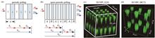
SignificanceMetasurfaces are composed of sub-wavelength electromagnetic resonator arrays, and they have attracted great attention because of their flexibly controlled polarization, amplitude, and electromagnetic phase of light waves at the sub-wavelength scale. At present, metasurfaces have experienced a fast-evolving development. Compared with traditional optical components, metasurfaces have obvious advantages and may become the most critical optical components to form a new generation of micro-optical systems, so as to provide a feasible way for miniaturizing and integrating optical systems. Unlike traditional refractive and diffractive optical components, metasurfaces have only a sub-wavelength thickness, which is thinner and can meet the increasing needs of miniaturized optical systems. Although the performance of metasurfaces has been highly extended by using various advanced design and fabrication methods, the practical application of metasurfaces is still limited by challenging large-area and high-throughput fabrication of sub-wavelength structures. All-dielectric metasurfaces based on semiconductor materials with a high refractive index have attracted more and more attention since they can be fabricated by using commercial complementary metal-oxide-semiconductor (CMOS)-compatible mass manufacturing technologies.Currently, nanoimprint lithography and deep ultraviolet lithography are widely used in CMOS-compatible mass manufacturing technologies, and researchers attempt to use them to realize the patterned growth of nanomaterials. However, due to the difference between materials, researchers need to develop new processes for each material. This paper mainly introduces the fabrication process and metasurface devices of each material, so as to help researchers choose convenient methods to fabricate metasurfaces.ProgressIn this paper, the background of high-throughput and large-area metasurface fabrication is introduced at first. In addition, compared with metal metasurfaces, all-dielectric metasurfaces have less energy loss and can be fabricated by using commercial CMOS-compatible mass manufacturing technologies, so all-dielectric metasurfaces are regarded as an optimal choice to achieve the large-scale application of metasurfaces devices. Furthermore, the existing challenges are discussed. Second, the fabrication method of silicon-based large-scale metasurfaces is introduced, including deep ultraviolet lithography and nanoimprint lithography. Relevant cases (Fig. 1 and Fig. 2) are analyzed, and the reason for applying these methods is explained. Then silicon nitride and titanium dioxide metasurfaces are analyzed in the same way. In addition, functional devices based on silicon nitride and titanium dioxide metasurfaces are also presented with details. Specifically, the aspect ratio of the titanium dioxide metasurface fabricated by nanoimprint lithography is as high as 7.8 (Fig. 8) in the part of other materials, and methods of fabricating perovskite and graphene are introduced with the specific examples (Fig. 9, Fig. 10, and Fig. 11). Finally, the limitations of these two methods are discussed. In addition, the femtosecond laser direct writing technology is studied, which may become a new generation of lithography. Additionally, the application and research direction of large-scale metasurfaces are predicted.Conclusions and ProspectsAlthough nanoimprint lithography and deep ultraviolet lithography have been used for fabricating high-throughput and large-scale metasurfaces and have received positive results, they still have many limitations, including the selectivity of substrate materials and complex processes. Therefore, a new method is required to address these issues. Femtosecond laser direct writing technology has some unique advantages, including extremely small heat-affected zone and high processing compatibility with transparent substrates. Besides, the femtosecond laser-induced direct patterned growth technology does not have such a complex process compared with deep ultraviolet lithography. Furthermore, processing efficiency can also be improved by adopting parallel processing strategies. For these reasons, femtosecond laser direct writing technology may become a new generation of lithography.
SignificanceMetasurface is a two-dimensional planar metamaterial composed of artificial sub-wavelength meta-atoms, and it can manipulate the wavefronts of electromagnetic waves. The rapid development of metasurfaces has spawned a variety of functional devices, including metasurface holography, metalens, vector vortex beam generator, polarization converter, etc. As can be seen, metasurfaces hold considerable promise for planar optical components and devices owing to their unprecedented ability to arbitrarily manipulate the amplitude, phase, frequency, and polarization of light. However, previous research on metasurfaces is based on passive metasurfaces with their intrinsic physical properties and structure parameters fixed and untunable after fabrication, which limits their practical applications such as dynamic control of the wavefront of light. As opposed to passive metasurfaces, the structure, properties, and functions of active metasurfaces can be tuned flexibly through external stimuli such as electricity, magnet, light, heat, and stress. With the help of active metasurfaces, the transmitted, reflected, or diffracted light can be dynamically manipulated by simultaneously or individually controlling the phase, amplitude, and polarization of light.ProgressRecently, many efforts have been devoted to studying various tuning methods-based tunable metasurfaces with multiple functions to dynamically manipulate and control electromagnetic waves as needed. The working principle of tunable metasurfaces mainly involves two mechanisms: one is based on active materials, while the other is based on nano-mechanical structural reconfiguration.The widely used active materials mainly include liquid crystals (LCs) and phase-change materials. LCs are active materials commonly used in optics owing to their broad tuning range of the refractive index. Recently, the combinations of LCs and plasmonic metasurfaces (Fig. 4) or dielectric metasurfaces (Fig. 5) are demonstrated with different functionalities including beam steering, zoom lens, and dynamic color display. The LC-based tunable metasurfaces have large modulation contrast and can cover the modulation range of 0-2π. In addition, LC-based metasurfaces have advantages such as high efficiency and low bias voltage requirements.Another commonly used active material refers to phase-change materials including but not limited to chalcogenide-glass and vanadium oxide. Thanks to their tunable optical properties induced by external stimuli, phase-change materials have emerged as a class of active materials integrated into the metasurface. In recent years, various chalcogenide-glass (Fig. 6 and Fig. 7) or vanadium oxide-based (Fig. 8 and Fig. 9) tunable metasurfaces are investigated in the field of tunable optical switch, perfector absorber, and beam steering. The phase-change materials-based metasurfaces have large modulation amplitude and wide phase modulation range owing to a large refractive index change during phase transition.Apart from active materials, tunable metasurfaces can be also achieved by nano-mechanical structural reconfiguration, such as flexible materials and microelectromechanical systems (MEMS). Recently, flexible materials (Fig. 10) and MEMS-based (Fig. 11 and Fig. 12) tunable metasurfaces are intensively studied, and their applications in zoom lenses, dynamic color display, and dynamic waveplates are explored. The flexible materials-based metasurfaces are relatively easy to be designed and fabricated, and they have several advantages such as a large phase modulation range (0-2π), large modulation depth, and high device efficiency. The MEMS-based metasurfaces have several advantages such as low loss, large modulation depth, the ability to cover the phase modulation range of 0-2π, high efficiency, and ease of integration with chips.Conclusions and ProspectsAlthough tunable metasurfaces have made significant progress, they still have low modulation speeds and are unable to control each element. Therefore, researchers need to make efforts in materials, fabrication technology, and design and optimization methods.First, new optical materials with large refractive index, faster response speed, higher sensitivity to external stimuli such as electricity, heat, light, and mechanical forces, and better compatibility with nanofabrication technologies are needed, so as to achieve faster and more accurate dynamic control of metasurfaces. In recent years, new materials such as conductive oxides, transition metal nitrides, Ⅲ-V semiconductor compounds, chiral materials, black phosphorus, and conductive polymers have attracted researchers' attention due to their excellent optical properties.Second, the nanofabrication technologies currently used for metasurfaces (such as electron beam lithography and focused ion-beam etching) are expensive and difficult to fabricate large-area metasurfaces with sub-wavelength-scale features due to long fabrication time and low yield. Therefore, a new nanofabrication technology that can balance yield, precision, fabrication time, and cost is urgently required. Nanoimprint lithography technology (especially ultraviolet roll-to-roll nanoimprint lithography) and projection lithography technology that can create large-scale nano-patterns in a short time are important research directions for subsequent metasurface fabrication.Third, the design and optimization of tunable metasurfaces require a system design framework from a single meta-atomic to macroscopic optical systems, which connects all key stages of material characterization, fabrication, and system operation in a coordinated manner. Topological optimization is a typical example of local optical optimization. Global optimization algorithms such as genetic algorithms (GA), ant colony optimization algorithms (ACO), particle swarm optimization (PSO), covariance matrix adaptation evolution strategy (CMA-ES), and multi-objective optimizers (MOO) have played an important role in the design and optimization of tunable metasurfaces. In addition, the rapid development of machine learning in recent years has provided a promising tool for optimizing optical metasurfaces. Using extracted metasurface structures and their corresponding optical responses to train neural networks can help to study the relationship between geometric structures and optical responses. This approach enables accurate and fast forward prediction of the optical response for a given metasurface, as well as application in inverse design where the desired optical response is used to deduce the device layout and characteristic parameters of the metasurface.
SignificanceThe high-power laser facility (HPLF) is the most sophisticated active optical system, whose performance is required to approach the physical limits. There are three primary procedures in designing HPLFs for research on inertial confinement fusion (ICF), namely, physical design, optical design, and mechanical design, in which optical engineering plays an important role. Optical engineering of HPLFs needs to follow its specific design principles and key points to achieve high output energy and precision beam quality. Given the final goal and feature of the laser facility, this paper describes the crucial technical issues in optical engineering development and their corresponding solutions from the aspects of the techniques for beam quality control, system alignment, target positioning, and associated technologies.ProgressThe high-power neodymium glass laser driver is internationally recognized as the most mature laser driver for physical research on ICF. It is also an indispensable and important platform for studies of high-energy-density physics and extreme-condition physics problems, as well as basic research on astrophysics. As one of the most representative giant optical projects in the world, the laser driver integrates advanced optics, laser technology, precision machinery, and computer control. Its scale and overall performance represent a country's highest level of laser technology and engineering. Many great powers of science and technology all over the world have carried out research on laser fusion and implemented the development plans of laser drivers, and several generations of HPLFs have been successively developed and built. The United States built the world's largest experimental device for laser fusion, i.e., the National Ignition Facility (NIF), in 2009. France is building a large-scale laser nuclear fusion device LMJ, which is similar to the NIF, and 56 laser beams in it have been operating at full power since 2019. Japan, the United Kingdom, and Russia have also built or are building smaller laser fusion devices. At the same time, China has successively built large-scale single-channel laser devices, six-channel laser devices, and ShenGuang (SG) series laser devices, playing a vital role in the international arena of ICF. With the development of HPLFs in China, the research on the laser driver, unit technology, and component technology has also been rapidly enhanced.HPLFs mainly include nanosecond (ns) laser devices and picosecond (ps) petawatt laser devices. The former outputs a ten-thousand-joule-level high-energy ns laser in a single channel, and the latter outputs a kilojoule-level high peak power ps laser in a single channel. The design of HPLFs consists of energy flow design and beam transmission design. The laser physics design of a laser driver is the first stage, followed by the optical engineering design and precision optical-mechanical structure design, and the final stage focuses on the development of the laser driver. This design logic indicates the important role of engineering optics in the development of laser drivers. An HPLF should meet the requirements of the output ability, beam quality, and beam-control ability proposed by physics. The device mainly contains several core indicators: energy, power, beam quality (focus spot distribution), waveform (time distribution), energy balance and power balance, as well as synchronization and target-hitting accuracy. Among them, beam quality and target-hitting accuracy are closely related to optical engineering design. Due to the large scale of HPLFs, long laser links, and large-caliber optical components, the various development processes need to be combined to satisfy the requirements of the above indicators, and the indicators of each subsystem must be reasonably allocated and strategically controlled throughout the system.The engineering optics of an HPLF has its particular traits. The device contains not only traditional static components but also dynamic components such as laser amplification and control components. Due to the thermal effect, the beam quality will be degraded after the laser passes through the amplifying element, and control measures are required to ensure the beam quality of the system. In addition, the high output energy of the device may cause damage to optical elements, and corresponding measures must be taken to minimize the risk of damage to ensure safe operation. Starting from the main considerations of engineering optics, i.e., optical design and ways to ensure the beam quality and target-hitting accuracy of the system, this paper summarizes the key scientific and technical issues concerning the engineering optics of the existing device. The overall optical design of the device is mainly to "set up the frame", establish the overall optical transmission chain of the device, and give the indicator requirements of components. The beam quality control is a "construction method", and linear and nonlinear transmission run through the entire laser device, which requires a whole picture of consideration. Specifically, the relationship between optical component indicators and beam quality should be clarified; the design, processing, and detection methods of special optical components should be determined; the corresponding optical detection means and active control methods should be matched; the residual wavefront and intensity unevenness of the system should be precisely controlled. In this way, the beam quality can be guaranteed. Target-hitting accuracy is the "foundation", which mainly provides decomposition methods for indicators and effective optical-axis control methods, and it cooperates with precise guidance and alignment technology.Conclusions and ProspectsAchieving controllable nuclear fusion and energy gain under laboratory conditions has long been a great dream pursued by scientists, and it is the most challenging major scientific project in the world today. The high-power laser driver for ICF and high-energy-density physical experiments has a powerful output ability of several megajoules of ns laser pulse energy, and it is equipped with tens of kilojoules of ps laser and corresponding output capabilities of 100 ps, femtoseconds (fs), or short wavelength laser pulses according to different physical demand. At present, powerful HPLFs are one of the focuses of the strong laser competition among the world's major countries. According to the design indicators and design characteristics of high-power laser drivers, this paper sorts out the key scientific and technical problems and corresponding solutions in optical engineering design in detail from the aspects of overall optical design, beam quality control, and target-hitting accuracy control. The research is expected to provide a reference for the engineering design of high-power laser drivers.
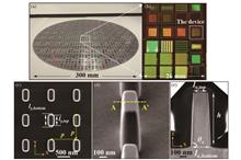
SignificanceThe detection of material composition on the surface of celestial bodies has always been an important content in lunar and deep space exploration. At present, the main detection means of material composition on the surface of celestial bodies is visible-near-infrared spectroscopy. Given the wide variety of material components on the surface of celestial bodies, attention should be paid to their chemical properties and content. The current single payload is difficult to meet these requirements, and it is necessary to develop new scientific payload technologies. Over the past two decades, the potential of Raman spectroscopy as a tool for lunar and deep space exploration has been intensively explored. Raman spectroscopy has the advantages of no need to prepare samples, fast and non-destructive analysis, and clear identification of molecular information. Thus, it is very suitable for the insitu detection of celestial bodies. Compared with visible and near-infrared spectroscopy, Raman spectroscopy has unique advantages in the detection of celestial surface materials. 1) The Raman spectrum peaks are clear and sharp without overlapping, which is conducive to the identification of minerals, especially for the composition and content measurement of mixed minerals. 2) It is not only easy to identify feldspar minerals, but also can detect other iron-free minerals. 3) It can detect inorganic substances, hydrous minerals, and organic substances at the same time. Therefore, Raman spectroscopy is a method with important application value and potential for the detection of material composition on the surface of celestial bodies, which complements the advantages of traditional visible light and near-infrared spectroscopy.ProgressSince the first commercial laser Raman spectrometer came out in 1987, Raman spectroscopy, as a powerful spectral analysis technique, has been widely applied in various material analysis fields. In 1995, Wang et al. first proposed the application of Raman spectroscopy on the lunar surface to detect its surface material composition. Subsequently, scientists successively proposed to apply Raman spectroscopy technology to the detection of extraterrestrial celestial bodies such as the moon and Mars and put forward optical probe type short-range detection Raman, long-range Raman, and time-resolved Raman. Raman spectrometers served as a potential payload in the Mars Exploration Rover mission of American and Tianwen-1 mission of China but ultimately were not adopted due to low technology maturity. With the development of lasers, charge-coupled devices, and other instrument components, the application of Raman spectroscopy technology to deep space exploration has become a reality.After years of verification of principle devices, various countries have added or plan to add Raman spectrometers to the payload queue for deep space exploration. The Perseverance Mars rover launched by NASA in 2020 is equipped with two Raman spectrometers SHERLOC and SuperCam. SHERLOC mounted on the robotic arm is a close-working deep-UV Raman and fluorescence spectrometer. The SuperCam is mounted on the mast and includes an image intensifier-based long-range time-resolved Raman spectrometer with a working distance of 7-12 m. ESA's Mars rover ExoMars is preparing to carry a Raman spectrometer RLS. RLS mounted inside the cabin is a close-range Raman spectrometer with an excitation wavelength of 532 nm. Japan's Phobos mission MMX is also preparing to carry the Raman spectrometer RAX. RAX mounted at the bottom of the rover is a close-range Raman spectrometer with an excitation wavelength of 532 nm. China's Chang'e-7 lunar exploration mission also plans a Raman spectrometer. The Chang'e-7 Raman spectrometer is a long-range time-resolved Raman spectrometer based on an image intensifier, with an excitation wavelength of 532 nm and a working distance of 1.2-3.0 m. Table 1 lists the parameter comparison of the above five Raman spectrometer payloads.This paper analyzes and discusses the key issues of Raman spectroscopy for deep space exploration. Due to the laser ablation limit of the material, there is a contradiction between the signal intensity of Raman spectroscopy and its spatial resolution. Long-range Raman spectrometers should focus more on signal strength, while close-range Raman spectrometers should focus more on spatial resolution. In terms of excitation wavelength selection, each excitation wavelength has its advantages and disadvantages. The most important thing in the selection of excitation wavelength is to consider the priorities of various scientific mission objectives. Fluorescence suppression is still one of the main problems faced by Raman spectroscopy. Infrared/ultraviolet excitation, time gating, frequency-shift excitation, and photobleaching are effective methods for suppressing fluorescence in deep-space Raman spectrometers. Raman spectroscopy technology for deep space exploration requires the support of many key components, and key components such as intensifiers and gratings still need to be developed.Conclusions and ProspectsRaman spectroscopy is a very powerful tool for detecting the composition of astronomical matters and is being applied by increasingly more deep space exploration missions. At present, the development trend of Raman spectroscopy technology for deep space exploration is modularization and miniaturization, multi-technology joint detection, long-range and short-range joint detection, and diversified detection fields.
SignificanceDiffractive optics is the most dynamic and potential branch of micro-optics based on diffraction theory. Diffractive optical element (DOE) is widely used in the design of optical systems as an element that modulates light waves through optimized structures. As DOE has the characteristics of light weight, easy replication, and high degree of freedom, and can achieve wavefront conversion, spectral modulation, array generation, and other functions that are difficult to be achieved by traditional refraction and reflection elements, it has become one of the research hotspots in modern optics. The characteristics of DOE can be widely combined with optical systems due to its compliance with the development trend of miniaturization and functional integration of modern optical systems. In addition, it has played an important role in modern industrial and national defense fields such as information processing, optical fiber communication, biomedicine, and space technology, and has shown broad application prospects.DOE based on scalar diffraction theory is the most widely used, and it has the characteristics of reasonable calculation and wide application ranges. In the process of combining with practical optical systems such as laser shaping, micro-measurement, and advanced processing, its design method has made significant progress in design theory, design process, optimization algorithm, and auxiliary design tools. The modeling, design optimization, pre-processing optimization, and evaluation analysis of DOE in typical optical systems can be realized.In recent years, there are a large number of interests in DOE designs and some reviews of DOE with a specific function or purpose, and the latest DOE design methods are required to be summarized. In order to promote the further development of DOE design methods based on scalar diffraction theory and better serve the development requirements of modern optical systems for structural compactness and functional integration, it is necessary to summarize the research progress of existing DOE design methods, discuss the problems restricting their further development, and prospect the future development trend, so as to provide reference and inspiration for the future research on DOE design methods.ProgressThis paper summarizes the design methods of DOE based on scalar diffraction theory. The basic principle of DOE design is reviewed, and the existing DOE design methods based on the diffraction principle and interference principle are briefly described. The specific DOE design methods and their applicability are described through several typical applications, and the technical difficulties in DOE design and the possible application direction in future science and technology are predicted.The scalar diffraction theory is applicable to the case where the feature size of DOE is much larger than the wavelength. The commonly used formulas include Kirchhoff diffraction integral formula based on point source and plane wave angular spectrum theory based on plane wave source. The scalar diffraction theory only considers the paraxial approximation of a single linearly polarized light but fails to discuss the vectorization and polarization coupling of the wave. It has the advantages of small calculation amounts, fast calculation speeds and can obtain the design results that meet the requirements of the optical system when the feature size is more than ten times larger than the wavelength.The design of DOE based on the diffraction principle is an inverse design problem. Since there is generally no analytical solution to this problem, it is necessary to solve the optimal solution through an optimization algorithm based on iteration, search, or deep learning (Table 1). The characteristics of the optimization algorithm in terms of convergence, initial value sensitivity, calculation speed, and whether the solution is the global optimum are critical, which largely determines the design efficiency and the proximity of the design solution to the real solution.The design of DOE based on the interference principle is a problem of obtaining an analytical solution through inverse decomposition. In terms of design, it can be summarized as the inverse decomposition problem of solving the interference sources with known interference light field. In terms of processing, it can be summarized as the inverse decomposition problem of solving the interference sources with known encoded light intensity distribution, where the interference source distribution can be any of amplitude, phase, or complex amplitude. DOE following this principle is often processed by holographic interference lithography.DOE is designed to be applied to practical optical systems, so the development of DOE design methods is closely related to the requirements of applications. Considering the functional requirements of DOE in the fields of light field regulation, wavefront modulation, spectral modulation, and imaging, this paper discusses the new development of DOE design methods in traditional application scenarios such as beam shaping and array generation, and summarizes the integration and development of DOE design methods and new system requirements in cutting-edge directions such as all-optical diffraction neural networks and extreme ultraviolet lithography masks. In addition, the main design methods of complex amplitude DOE and dynamic DOE are summarized from the perspective of the development direction of DOE as an optical element.Conclusions and ProspectsAfter years of theoretical design and practical requirements of DOE for optical systems, DOE design methods based on scalar diffraction theory have made important progress in the theoretical model establishment, optimization algorithm development, and joint optimization with processing technology. However, in the face of higher diffraction efficiency, higher modulation accuracy, wider spectrum and temperature range, and more diverse functions of optical systems, the existing design methods still have problems of slow design speed, complex design process, and limited design freedom. In the future, the universality, accuracy, and applicability of DOE design methods can be improved by innovating physical models, learning from other fields, and integrating the advantages of existing optimization methods. It is expected that the well-designed DOE will play an increasingly important role in fields such as biomedicine, AR display, and space technology.
SignificanceAberration correction results and imaging performance of the optical systems are partly determined by the mathematical description method of the optical element surfaces. For example, a lens with the surface described by an even asphere equation can effectively correct the spherical aberration. Also, the mathematical expression determines the speed of ray tracing and optimization convergence affects the difficulty in surface processing and testing. Hence, it affects the overall development cycle and cost of the optoelectronic system. It is important to explore the novel optical surface description method to obtain an optical imaging system with higher performance. The optical surface should have more degrees of freedom to describe the complex shapes and correct the optical aberrations, and the optimization of the parameters should converge quickly with an acceptable result in the design process.Since the 16th century, researchers have been investigating description methods of the optical surface. Especially since the end of the last century, various novel description methods have been proposed. They have played an active role in different optical systems and have effectively improved the system's performance. Novel optical surfaces are effective in practical applications such as periscopes, progressive addition lenses, viewfinders, remote sensing, projection, and lithography.Optical surfaces can be divided into two categories: explicitly and implicitly defined surfaces according to the mathematical expression. In the process of optimization, it is necessary to calculate the intersection point of the rays with the surface and the first partial derivative of the surface at the intersection point to determine the propagation direction of the rays after passing through the optical surface. For surfaces with explicit definitions, it is easy to get the calculation result through explicit expressions. However, for surfaces with implicit definitions, finite difference or other methods are utilized to trace rays. Hence, the ray tracing speed of an explicitly defined surface is larger. Almost all optical surfaces are defined by explicit expressions. A typical implicitly defined surface is a non-uniform rational B-Spline surface.Depending on the effect of parameters on the sag of the surface, mathematical descriptions of optical surfaces may be local or global. For the global descriptions, the sag and partial derivative on the whole surface will be changed when the arbitrary parameter of the optical surface is adjusted. The local descriptions have a more powerful ability to tune the local shape. Each parameter of local descriptions has a limited range of influence on the shape of the surface, so the local curvature of the surface can be adjusted without affecting the shape of the surface outside its area of action. Spline surface, Gaussian basis function surface, and wavelet function surface are local descriptions. Moreover, the stitched surface also can be considered a local description.To control the surface shape effectively, designers would like to use the low-order parameters of the mathematical descriptions during optimization. However, from a macroscopic point of view, this approach reduces the degrees of freedom, which goes against the original intention of using a complex optical surface to be flexible and more descriptive. If the designer can control the surface shape strongly, it may be bold to optimize the optical system with high-order parameters. The surface shape of a complex optical surface can be constrained by controlling the first and second partial derivatives and the local Gaussian curvature of the optical surface.To meet the design requirements of optical systems with high performance, it is necessary to extend the mathematical description and design methods of optical surfaces. Complex optical surfaces with additional degrees of freedom can effectively improve the performance of the optical system.ProgressThe developing status of mathematical description and design methods for complex optical surfaces is summarized. First, the mathematical description methods of optical surfaces are briefly discussed. Currently, most mathematical descriptions of optical surfaces are global and explicit. For optical surfaces with explicit definitions, Cartesian coordinates are generally applied to model them (Fig. 1). The mathematical expression of a complex optical surface can be decomposed into two main parts: the base term and the deformation term. Sphere, conic, and bi-conic are common basic terms, which mainly contain the second-order components and express the main shape of the surface. Deformation terms, such as polynomials, describe additional, and asymmetric surface shapes are responsible for the aberration correction. Then, the state of the art and progress in the mathematical description of optical surfaces are elaborated. With the increasing complexity of optical systems, conventional spherical and aspherical surfaces severely lack degrees of freedom and are hard to meet design requirements. Researchers have proposed various expressions to describe optical surfaces. The basic terms and complex optical surfaces are listed separately. Subsequently, methods on how to control the local or global shape of complex optical surfaces are introduced. Controlling the shape of complex optical surfaces is important. On the one hand, it ensures the manufacturability and detectability of optical components. On the other hand, a reasonable shape can save processing time and costs. In the end, the mathematical formalisms of the novel optical surfaces are given. Practical examples are listed to demonstrate the feasibility and effectiveness of these surfaces. The future research directions for the mathematical description method of the complex optical surface are discussed and analyzed.Conclusions and ProspectsBenefiting from the development of processing techniques, complex optical surfaces are widely applied in practice. In summary, the mathematical description and design methods of complex optical surfaces still need in-depth and detailed explorations to promote the achievement of high-performance optical systems.
SignificanceOver the last decade, the performance of space optical systems has been significantly improved through the efforts of optical researchers in China and abroad. Two critical specifications of an Earth Observing (EO) system are resolution and swath. By this measure, China's recently launched commercial EO systems have reached a world-class level. These inspiring achievements are the results of courageous innovations and substantial practices in reflective optical materials, optical design, aspheric fabricating and testing, and system assembly.Advanced manufacturing technologies of optical systems include mirror blank preparation, optical design, fabrication, coating, testing, and system assembly, which is an enabling technology for high-performance optical systems. The imaging optical system is an information collecting system rather than a simple energy collecting system. An important indicator to assess its performance is the information collecting capacity. For example, the requirements for the EO payloads are higher resolution and wider imaging swath. However, constrained by launch costs and working environments, the volume and mass of space optical systems are strictly restricted. Therefore, some common requirements for its manufacturing technology are summarized as follows. First, the mirror materials should have high specific stiffness and thermal deformation resistance to reduce the cost of launch mass and thermal control. Second, the systems with large aperture, long focal length, and large field of view (FoV) simultaneously are needed to solve the contradiction of high resolution and wide swath, and this results in multiple-mirror on-axis or off-axis design. Aspheric surfaces or even freeform surfaces are employed to increase the design freedom and balance the large off-axis field aberrations. Nevertheless, the off-axis aspheric or freeform design causes asymmetric mirror shape and system layout. Consequently, unlike the conventional slow lapping process, the deterministic computer-controlled optical surfacing (CCOS) technique is necessary to achieve higher accuracy and efficiency. Meanwhile, aspheric surface digital testing and system computer-aided alignment techniques are utilized through the whole process of milling, grinding, polishing, and system assembly to guide deterministic processing and verify the payload's performance consistency in space and on earth.In this paper, the latest progress of space optical systems over the last decade in China are introduced with the combination of several on-orbit examples. The technological advantages include silicon carbide (SiC) material, space optical system design and configuration evolution, digital measurement of complex optical surfaces, and computer-aided assembly and adjustment technology. In addition, the future trend of advanced optical system manufacturing technology is discussed.ProgressThe space qualified mirror materials should be easy to manufacture and of high dimensional stability to adapt to the working environments. Compared with optical glass and some metal materials, SiC ceramics exhibit excellent performance in specific stiffness and thermal stability (Table 1). For large-aperture space telescopes, reflective systems have been widely applied for their mirror light-weighting nature and chromatic aberration-free feature. Two-mirror systems are adopted traditionally in the early applications such as Ritchey-Chretien (RC) system (Fig. 5). Several designs based on three-mirror layouts have emerged in the 60s and 70s of 20th century to further correct astigmatism and increase the available FoV, and the most successful example is the three-mirror anastigmat (TMA) proposed by Korsch (Fig. 6). To further increase the field of view and correct the higher-order off-axis aberrations, this paper introduces freeform surfaces based on the conventional TMAs. The optical payload in GF-6 satellite is an off-axis four-mirror design, in which the second-and-fourth mirror employs the Zernike freeform surfaces (Fig. 11). The rapid development of advanced manufacturing technology has been greatly promoted with the evolution of complex optical system configurations. The CCOS, magnetorheological finishing (MRF) and ion beam figuring (IBF), and other advanced manufacturing technologies have been developed and applied to manufacturing aspherical optical systems (Fig. 16) with extremely high shape accuracy (Fig. 19). In addition, the aspheric surface testing methods have been developed and utilized in a combined way to measure the surface shape (Figs. 22 and 23). Finally, based on the co-reference alignment technology using computer-generated hologram (CGH), some testing results of the aligned system are shown (Figs. 25-26).Conclusions and ProspectsThe advanced optical manufacturing technology based on multi-axis computer numerical control machining center has yielded remarkable results and has been extensively applied in numerous projects. However, for very large aperture monolithic or segmented mirror telescopes, optical manufacturing faces challenges in high quality and volume productions. On one hand, 8 m class aspheric or freeform mirrors need to be manufactured to the accuracy of sub-10 nm RMS. On the other hand, hundreds of 1 m class aspherical segmented mirrors need to be polished with high efficiency and consistency. In the future, an optical intelligent manufacturing system will be constructed with the combination of intelligent decision support, process sensing, collaborative manufacturing based on big data, cloud computing, and machine learning. The unmanned workshops together with intelligent green flexible manufacturing technology are highly expected in the following decade.
SignificanceFreeform surfaces are optical surfaces without linear or rotational symmetry. Their flexible surface geometry offers high degrees of freedom, which can be employed to avoid restrictions on surface geometry and create compact yet efficient designs with better performance. Therefore, freeform surfaces can endow beam shaping with more new functions and satisfy the ever-growing demand for advanced beam-shaping systems.The design of freeform beam-shaping optics can be formulated as follows. Given an input (a light source) and an output (a prescribed irradiance/intensity distribution), one or multiple freeform surfaces are to be designed so that the light rays emitted from the source are redirected to produce the prescribed irradiance/intensity distribution. According to the étendue of the light source, the design of freeform beam-shaping optics can be divided into two groups, i.e., zero-étendue algorithms based on ideal source assumption and design algorithms for extended light sources. The zero-étendue algorithms assume that the spatial or angular extent of the light source is zero, which means that only one single ray passes through each ray-piercing point on the optical surface. However, the situation becomes different when the étendue of the light source is non-zero. There are an infinite number of light rays passing through each ray-piercing point on the optical surface. When the influence of the spatial or angular extent of a light source on the performance of the beam-shaping system can be ignored, the light source can be considered as an ideal source (a point source or a parallel beam). Then, the design of freeform beam-shaping optics can be greatly simplified by zero-étendue algorithms. Additionally, as the extended light source can be considered to be composed of an infinite number of ideal light sources, most of the current designs of freeform beam-shaping optics are involved in zero-étendue algorithms.The zero-étendue algorithms include three typical methods including the ray mapping method, the support quadratic method (SQM), and the Monge-Ampère (MA) method. A key step in the ray mapping method is to find a ray mapping that can satisfy the integrability condition. Finding such an integrable ray mapping may not be a simple task. The SQM is a process of calculating a set of quadric surfaces which are employed to build a freeform surface, which produces a discrete illumination that is an approximation to the prescribed illumination. This method can achieve very complex irradiance/intensity distributions, but it requires tens of thousands of quadratic surfaces to construct smooth and continuous freeform surfaces. In addition, the effectiveness of this method still needs to be further explored when multiple freeform surfaces are needed. The MA method converts the design of freeform beam-shaping optics into an elliptic MA equation with a nonlinear boundary condition. This method reveals the mathematical essence of freeform optics design based on the ideal source assumption. It can satisfy the integrability condition automatically and can be implemented efficiently. Its effectiveness has been proven in a wide variety of applications, and the superiorities are verified in LED and collimated laser beam shaping.ProgressIn 1972, Schruben converted a prescribed irradiance design with a freeform reflector into a highly nonlinear partial differential equation of second order and proved that such a differential equation of second order is an MA equation. In 2002, Ries demonstrated that a prescribed irradiance design with a freeform lens can be converted into an MA equation based on the relationship between the power density and the curvature of the wavefront. This method can be adopted to tackle complex designs without any symmetry. Finding the solution to the MA equation is a big challenge. Unfortunately, Ries did not introduce the method leveraged to find the solution and did not disclose any further studies on this method in the subsequent ten years. Thus, other researchers in this field had to explore some new ways to solve this inverse problem. In 2013, Wu converted the design of freeform beam-shaping optics into an MA equation and a nonlinear boundary, and first disclosed a numerical method to solve the MA equation. Over the last ten years, Wu generalized the MA method to achieve freeform and precise irradiance tailoring in arbitrarily oriented planes, and to design freeform optics for flexible and precise control of the intensity and wavefront of a light source.Conclusions and ProspectsThe MA method relying on the ideal light source assumption is considered as the most advanced point source algorithm that satisfies the integrability condition automatically and can be implemented efficiently. Additionally, it can be generalized to design freeform beam-shaping optics for extended light sources since an extended source can be considered to consist of an infinite number of ideal light sources. The MA method paves a way for the broad application of freeform optics.
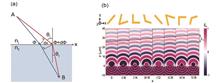
SignificanceAs one of the important optical components in optical systems, lenses are widely used in products for imaging, illumination, and optical communications. In general, lenses can be divided into spherical, aspheric, freeform, and microstructure surfaces according to different surface shapes. Among them, the spherical lens is the simplest optical component in terms of design and manufacturing, but the aberration problem exists when a single lens is used, and the bulky lens assembly has to be used for compensation. In contrast, aspheric and freeform lenses have more flexible surface shapes, and the specific optical performance of lenses can be improved by such methods as aberration correction, beam shaping, and field of view expansion, which are beneficial for realizing high precision and integration of optical systems.Optical glass and plastic are the main raw materials for lens manufacturing. Plastic is more economic and lighter, but glass has better mechanical properties, higher thermal stability, and higher refractive index, which meets the demanding requirements of optical performance and stability for most products. High-precision glass spherical lenses have achieved mass production by grinding and polishing, but aspheric, freeform, and microstructure lenses can only be processed one by one with the traditional subtractive manufacturing methods for their complex and irregular shapes. In some cases, even several non-traditional polishing methods such as magnetorheological finishing (MRF) and ion beam polishing (IBP) have to be used to produce high-precision surfaces, which is time-consuming and costly. Therefore, an effective and low-cost processing method is required for the mass production of such lenses.Molding is a classical processing method to produce parts by replicating the mold shape. However, conventional fused silica glass was not friendly to the mold life for its high transition temperature (about 1300 ℃), which limited the development of glass molding. Until the 1980s, glass with a low transition temperature emerged, and it could be molded at 300-700 ℃, which promoted the rapid development of glass molding. Nowadays, precision glass molding (PGM) has become a main technology to realize the mass production of glass optical components and the manufacturing of numerous aspheric lenses and partial freeform and microstructure lenses, which only takes a few minutes for one lens. PGM has significant advantages over traditional manufacturing technologies, such as low costs, low pollution, high efficiency, and net shapes, which presents superior development potential.PGM is a complex process affected by factors such as glass material properties, mold manufacturing, process parameters, and molding machines. As higher requirements for shape complexity and quality of lenses are posed, many problems have been exposed and aroused the interest of researchers. There are many advances in glass, molds, machines, and numerical simulations. Therefore, it is important to summarize the current progress and prospect the development trend and challenges of PGM.ProgressThis study introduces the principle of PGM for glass optical components and elaborately summarizes the recent progress in glass material development, mold manufacturing, molding process optimization combined with finite element simulation, and molding machines.Firstly, various glass materials and glass constitutive models including the Maxwell model, Kelvin model, Burgers model, and generalized Maxwell model are introduced (Figs. 5 and 6), and the modeling methods of creep and stress relaxation are analyzed.Secondly, the properties of various mold materials are compared, among which tungsten carbide has the best overall performance (Table 1). Ultra-precision grinding, cutting, etching, and polishing are the main methods to produce high-precision molds. The newly developed off-spindle-axis spiral grinding method is employed to fabricate the aspheric micro-lens array (Fig. 9), and an effective laser-assisted turning method is proposed to achieve the rapid mold machining (Fig. 12). Subsequently, the typical film materials for molds are compared (Table 2), and the high-hardness Ta-C film is deposited on the mold by the filtered cathodic vacuum arc method, which shows low friction and wear. The degradation mechanism of the noble metal Pt-Ir film and its optimized structure are presented (Fig. 17).Thirdly, numerical simulation is applied to analyze temperature, stress, friction, and surface shape accuracy in molding. Various molding machines including the single-workstation machine, multi-workstation machine, and ultrasonic vibration-assisted glass molding machine are introduced, and it is found that the multi-workstation machine is more suitable for mass production. The profile accuracy of microgroove molding by the ultrasonic vibration-assisted machine is also improved (Fig. 31).Finally, the pioneering studies on molding lenses with flexible and complex surfaces such as freeform and microstructure lenses, as well as lens wafer arrays are summarized.Conclusions and ProspectsIn summary, PGM has been widely employed to produce lenses with aspheric and various flexible surfaces. Technologies in the field of glass material, mold manufacturing, numerical simulation, and molding machines have developed comprehensively and made great progress. However, as the demand of freeform components as well as microstructure and wafer array lenses is increasing, it still faces many challenges in molding complex surfaces in mass production. In the future, these difficulties will be gradually solved, and PGM will become more advanced with high-performance glass and mold materials, effective mold manufacturing technologies, integrated numerical simulation, and external energy field-assisted molding technologies.
SignificanceImaging optical systems have been widely used in industrial, medical, and military fields. With the rapid development of modern science and technology, the increasing requirements for imaging optical systems in various applications have promoted the development of optical systems towards higher performance, better imaging quality, smaller volume, lighter weight, and more novel and richer functions. However, it is difficult for traditional spherical and aspheric imaging optical systems to meet these requirements. Therefore, optical freeform surfaces are used in imaging optical systems.Optical freeform surface is a kind of surface without rotational symmetry. Compared with spherical and aspheric surfaces, freeform surfaces have more degrees of freedom for design and stronger aberration correction ability. Thanks to these excellent characteristics of freeform surfaces, high-performance, compact, lightweight, and novel optical systems have been successfully designed and applied in astronomical telescopes, spectral analysis, remote sensing, and virtual reality. The application of freeform surfaces brings many benefits to optical systems, but it also inevitably destroys the rotational symmetry of the optical systems, which poses a great challenge to traditional optical system design methods.In order to realize the efficient design of freeform optical systems, people not only extend the design methods based on traditional aberration theory but also propose some direct design methods which can directly obtain the parameters of freeform surfaces according to the system specifications. These methods can provide favorable initial structures for further optimization. In addition, some automatic design methods for optical systems whose imaging quality is close to the diffraction limit are proposed. But these design methods still have some limitations. Therefore, it is necessary to summarize the existing design methods of freeform surface imaging optical systems to better guide the future development of this field. At the same time, the progress of freeform surface design methods can promote the design of freeform surface optical systems. Therefore, it is very important to classify and summarize the existing applications of freeform surface imaging optical systems to better help people optimize their designs.ProgressThis paper introduces various design methods of freeform surface imaging optical systems in detail. Firstly, the limitations of designing optical systems based on traditional aberration theory are discussed. The nodal aberration theory proposed by Shack and Thompson is introduced. The advantages of nodal aberration theory in aberration analysis and optimization guidance of freeform surface imaging optical systems are summarized. Then the research progress and technical characteristics of various direct design methods are introduced in detail, including differential equation design method, simultaneous multiple surface design method, construction-iteration design method, series expansion design method, and design method based on machine learning. The differential equation design method is used to design the freeform surface, and its mathematical theory is relatively complete. The simultaneous multiple surface design method can directly design multiple surfaces at the same time. The number of surfaces usually equals that of fields of view that can be controlled by this method. The construction-iteration design method is highly versatile, and the light rays from multiple fields of view and different pupil coordinates are considered (Fig. 4). The series expansion design method uses power series to solve functional differential equations, which has a fast calculation speed. The design method based on machine learning combines the machine learning algorithm with the process of optical design, which can obtain a large number of design results with little manual participation. Then the automatic design methods of the optical systems which can directly and automatically obtain the imaging quality close to the diffraction limit are introduced. Finally, the advantages and limitations of different freeform surface imaging system design methods are compared (Table 1).This paper also summarizes the applications of freeform surface imaging optical systems with high performance, as well as new structures and functions in various fields. Firstly, the early applications of freeform surfaces in imaging optical systems are reviewed, including the deformable lens designed by Chretien, the Alvarez lens with variable focal length, and the viewfinder of the Polaroid SX-70 camera. Then several high-performance freeform surface imaging optical systems are introduced, including off-axis reflection systems with a large field of view, low F number, or small volume (Fig. 8), imaging spectroscopy systems with higher spectral resolution and better imaging quality (Fig. 11), and extreme ultraviolet lithography projection systems with extremely high imaging quality and extremely low distortion (Fig. 13). Then, several kinds of freeform surface imaging optical systems with new structures and functions are introduced, including off-axis reflection systems with special structures such as primary mirror and tertiary mirror integration (Fig. 14), visual optical systems for head-mounted display and head-up display (Fig. 15), optical systems with local optical properties (Fig. 16), and freeform optical systems with lateral image translation or other special functions.Conclusions and ProspectsDesign methods of freeform surface imaging optical systems have made great breakthroughs and may develop towards the following directions in the future, including automatic design, rapid design, combination with machine learning, and consideration of both design and process. With the continuous research and improvement of the design methods of freeform surface imaging optical systems, more and more freeform surface imaging optical systems have been designed. At present, the specific applications of freeform surface imaging optical systems mainly have the following development directions, such as higher performance, more novel functions, and newer structures. At the same time, these freeform surface optical systems with high performance and new functions will put forward higher requirements for the processing, metrology, and alignment technologies of freeform surfaces. The progress of these technologies will also continue to promote the development of freeform surface imaging optical systems.
SignificanceFreeform surfaces have been regarded as one of the major revolutions in the field of modern precision optics. They are expected to further promote miniaturization, lightweight and integration of optical systems due to their excellent optical and mechanical properties. The quality of machined freeform surfaces will significantly influence the performance of optical systems. Surface metrology including the measurement of surface texture and surface form errors is the important post-manufacturing part to determine which surface can be employed. In the past decades, various methods have been developed for measuring and characterizing freeform surfaces, mainly including probe-based scanning, full-aperture optical inspection, on-machine measurement technology, feature-based surface registration and multi-scale data fusion methods. Although many corresponding advances have been achieved, great challenges are posed to the quality of surface manufacturing with the complexity of freeform surfaces increasing. Moreover, the surface form error is required to be lower than 0.1 μm and the surface roughness should be less than 1 nm. It is urgent to develop a new measurement technology for achieving a higher dynamic range and a higher accuracy. Hence, it is important and necessary to summarize the existing research to guide the future development of this field more rationally.ProgressMeasurement and characterization of optical freeform surfaces are the key processes to check the quality of freeform surfaces. The widely used techniques related to these two processes are summarized. Firstly, the precision measurement methods for optical freeform surfaces are introduced, including probe-based scanning, full-aperture optical inspection and on-machine measurement. The probe-based scanning methods include nanoscale 3D coordinate measuring machine, non-contact profile scanner and swing arm profilometer. To further improve the dynamic and precision measurement performance of coordinate measuring machines, Manske's research group from Technische Universit?t Ilmenau, Germany, has conducted relatively pioneering studies by using an atomic clock-stabilized He-Ne laser via a high-stable-frequency comb. Secondly, full-aperture optical inspection methods are elaborated, including null test metrology of computer-generated holography (CGH), sub-aperture stitching test and adaptive interferometry. Subsequently, surface characterization processes such as surface registration, data fusion and error evaluation are reported. The iterative closest point (ICP) algorithm and its modified methods have been surveyed by Maiseli and Zhu. Liu and Wang from the Hong Kong Polytechnic University have engaged in plenty of studies on multi-sensor data fusion based on Gaussian processes (GP) after reliable surface registration. Jiang's team from the University of Sheffield summarized and expounded on the new application methods of characteristic parameters for complex freeform surfaces. Considering the latest application of freeform surfaces, a novel method is also presented for measuring and evaluating new freeform types called conjunctive multi-freeform surfaces. In the end, the problems and the ongoing research trends in this field are discussed, including measurement means and surface characterization techniques.Conclusions and ProspectsRapid, accurate and reliable inspection technology is the core factor to judge whether the performance of an optical freeform surface meets the requirements of intelligent manufacturing. In the measurement process, the widely used point-line-based scanning measurement method can achieve high measurement accuracy and realize the measurement of micro-nano structure, large-scale surface, and local features with high steepness. However, the measurement efficiency is low and the optical surface may be scratched during contact measurement. In contrast, full-aperture measurement methods have the superiority of fast measurement and high accuracy without contacting the surface. However, the lateral resolution of these methods needs to be further improved and the dynamic range of measurement is limited. Combining the advantages of the two types of measurement technologies is a promising way to improve manufacturing efficiency. As a result, on-machine measurement technology integrating multiple measurement methods to realize the multi-sensor in-situ measurement of complex surface shapes has become the development trend of the current measurement field.On the other hand, in the error evaluation process, ICP and its modified technologies have always been the first choice for surface registration. Although it is influenced by the initial value, the registration method combined with the inherent characteristics of optical freeform surfaces or the auxiliary datum constructed basically meets the accuracy requirements. However, the computational complexity and efficiency still need to be improved. For multi-sensor data, data fusion mostly depends on linear fitting. The associated characteristics of the fusion process remain to be further explored. The deep fusion of multi-source data may become an important direction in this field by combining with the machine learning technique. In the future, with the rapid exploration of multifunctional, micro-nano and multi-scale optical surfaces, the corresponding measurement and surface characterization methods may encounter new challenges in the manufacturing of optical freeform surfaces.
ObjectiveLidar is widely applied in 3D imaging because of its high precision, high resolution, and long working distance. The size and distribution of the illumination spot on the imaging target are important factors affecting the imaging resolution. The smaller spot size results in finer information obtained on the target surface and clearer 3D information of the reconstructed object. The increase in spot size affects the quality of laser scanning 3D imaging mainly in two aspects. On one hand, it will reduce the energy of light signals shining on the surface of the object, thereby leading to weakening return light signals and affecting the detection distance. On the other hand, the area of large light spot shining on the object surface is also large, which causes multiple echo signals generated by the same light spot due to the change of object surface, thus affecting the ranging accuracy. However, most of the existing lidars employ collimated Gaussian beams to emit. When imaging at a long distance, the spatial resolution is significantly reduced with the increasing target distance due to the laser divergence angle and the diffraction limit of the optical system. To this end, this paper improves the system resolution from the aspect of output beam control and scanning mode.MethodsIn laser scanning 3D imaging, the beam scans and illuminates the target point by point, and detects the return light signals at different positions of the target to obtain the depth information of the detection target surface and realize 3D imaging. In this process, the traditional laser scanning 3D imaging generally irradiates the laser collimated and expanded to a distant target object in a parallel beam mode for reducing the divergence of beams. The size of the light spot at the target object mainly depends on the divergence angle of the beam after expansion and the imaging working distance and is generally far greater than that of the light spot under the diffraction limit. By changing the focal length of the system, this paper focuses the light spot at the imaging target to obtain a small light spot. Sub-pixel scanning is originally proposed as a method to obtain high-resolution (HR) images from multiple low-resolution (LR) images for ordinary digital cameras. In sub-pixel scanning technology, the basic premise to improve spatial resolution is to capture multiple LR images from the same scene. LR images are subsampled (aliased) and shifted with sub-pixel accuracy. If the LR image is shifted in integer units, each image contains the same information, so there is no new information available to reconstruct the HR image. However, if LR images have different sub-pixel offsets from each other and there is aliasing, HR images can be obtained using the new information contained in each LR image. As an analogy to lidar, sub-pixel scanning can also be employed to enhance the imaging resolution of the system.Results and DiscussionsA confocal sub-pixel scanning photon counting lidar is designed to improve the spatial resolution of the system. The size of the focused spot at 10 m is about 1/4 of that of the collimated spot. Compared with pixel-by-pixel scanning, 1/8 sub-pixel scanning at 7 m and 10 m can recover the letter I on the resolution target (Fig. 4). Focused lighting can effectively enhance echo energy (Fig. 5) and imaging resolution (Fig. 6) compared with collimated lighting. Combined with sub-pixel scanning, the imaging resolution of the system is increased from 5.0 mm to 0.9 mm, which exceeds the diffraction limit of the system. In addition, with the decreasing sub-pixel scanning step, the imaging resolution will also be improved. The experimental results show that through sub-pixel scanning, the aliasing of the reconstructed image is rapidly reduced, and the contour is smoother and more accurate (Fig. 8).ConclusionsThis paper demonstrates the sub-pixel scanning high-resolution technology using collimated and focused illumination through experiments. The imaging results of the transmissivity resolution target show that under the same FoV, small spot illumination can effectively improve the imaging resolution. The reconstructed image obtained by sub-pixel scanning is smoother and clearer than the pixel-by-pixel image. The horizontal resolution is increased from 5.0 mm per pixel for collimated illumination to 0.9 mm for focused illumination with sub-pixel scanning and exceeds the limit of system angular resolution. In addition, in the lidar system, the resolution improvement of sub-pixel scanning is also related to the spot size. Small spot illumination and sub-pixel scanning technology have great potential in improving the spatial resolution of long-range lidar.
ObjectiveWhile space-variant micro/nano structures are segmented or interleaved in a two-dimensional plane, they demonstrate integrated performance as a multi-function or multiplexing meta-device. Among present technologies, projection lithography and interference lithography are effective for the rapid fabrication of micro/nano structures. By high-resolution masks, projection lithography produces space-variant micro/nano structures quickly. However, the area of its fabricated micro/nano structures is seriously limited by variation ranges of parameters. For interference lithography, the structural profile and period can be varied by changing intensities and interference angles of light beams, respectively. Nevertheless, their corresponding micro/nano structures change in a limited range with low resolution, in addition to their complex optical setups. Combining projection lithography with interference lithography, this paper reports an optical Fourier transform system modulated by phase element to dynamically produce micro/nano structures in a wide variation range and achieves structural period variation of less than 1 nm. It merely produces structures pixel by pixel and dimension of every pixel is constant. Then, space-variant phase element is utilized as the phase element, where multi-interference light fields are generated to fabricate different micro/nano structures in different shaped pixels. However, their structural parameters and pixels cannot be customized or changed in real time. Therefore, this paper proposes a method to parallel produce micro/nano structures with independent changed structural parameters and pixels, which can be utilized to generate flexible arranged space-variant micro/nano structures for multi-function or multiplexing meta-devices.MethodsAn optical Fourier transform system jointly modulated by aperture diaphragms and a phase element is proposed. With the Fourier transform principle of lenses and the geometric propagation characteristics of diffraction beams in the phase element, the generation and manipulation of multi-interference light fields in the imaging plane are discussed. The theoretical analysis shows that multi-interference light fields are determined by the distributions of aperture diaphragms and the transmission of phase elements, where the pixelated aperture diaphragms are responsible for the distribution of light fields, and the transmission of a phase element contributes to the structural parameters of each interference light fields. Furthermore, the magnification between the imaging plane and the aperture diaphragm plane as well as the one between the image plane and the transmission plane of a phase element is different, which means that the variation in aperture diaphragms and the phase element manipulates the interference light fields independently. Then, two methods for the generation and manipulation of multi-interference light fields are discussed. When modulated by multi-pixel aperture diaphragms and a phase element, multi-interference light fields are generated to parallel produce the same structure within different pixels. Pixels and the infilled structural parameters can be dynamically changed by varying aperture diaphragms and manipulating the phase elements. When modulated by multi-pixel aperture diaphragms and a space-variant phase element, multi-interference light fields are generated to simultaneously produce different structures within different pixels. The same rules are obeyed in the manipulation of the light fields except that the change in the aperture diaphragms can vary the structural pattern inside each pixel. Therefore, incorporating the analyzed methods and rules for the generation and manipulation of the interference light fields, aperture diaphragms and the phase element can be inversely designed to produce customized light fields for flexible assembled micro/nano structures.Results and DiscussionsWith the inversely designed methods mentioned above, symmetrical rectangular apertures are utilized as aperture diaphragms and a grating eliminating 0th transmission is acted as the phase element (Table 1) to modulate an optical Fourier transform system. Theoretical results show that three segmented interference light fields with targeted fringe frequency are produced simultaneously, while their light field distribution and interfered fringe frequency change as expected by pre-designed variation in apertures and the position of the grating (Fig. 5). Meanwhile, multi-pixel apertures and a grating with space-variant orientations are designed to modulate the Fourier transform system, and types of demand-interleaved interference light fields are generated for the fringes with their orientations flexibly arranged (Fig. 7). Experimentally, aperture diaphragms and phase elements fabricated as designed are placed in the optical Fourier transform system, and segmented/interleaved interference light fields, coincident with the theoretical ones, are detected in its imaging plane (Fig. 9). Combining the multi-interference light fields with the miniature projection, arrays of segmented nano-gratings are fabricated consequently. With the time division multiplexing of dynamically controlled multi-interference light fields, segmented nano-gratings of nine pixels are fabricated with measured pixel dimensions of 142.705 μm×142.689 μm, 75.102 μm×75.264 μm, 27.576 μm×27.505 μm as well as structural periods of 472 nm, 375 nm and 275 nm (Fig. 10).ConclusionsIncorporating planar segmented or interleaved space-variant micro/nano structures, meta-device demonstrates multi-function or multiplexing performance. To fabricate customized distributed and space-variant micro/nano structures with interference, this paper proposes an optical Fourier transform system, which is jointly modulated by aperture diaphragms and a phase element. With the Fourier transform principle of lenses and the geometric propagation characteristics of diffraction beams in the phase element, the methods for the generation and manipulation of flexibly distributed multi-interference light fields in the imaging plane are analyzed. Apertures and a grating, as well as apertures and a grating with space-variant parameters, are inversely designed as aperture diaphragms and a phase element respectively to obtain the required distribution of variant micro/nano structures. Theoretical and experimental results verify that with the inversely designed aperture diaphragms and the phase element modulating the optical Fourier transform system, target interference light fields for arrays of segmented or interleaved micro/nano structures can be realized. Combined with the multi-interference light fields and the miniature projection, arrays of segmented nano-gratings are fabricated in sequence. With the time division multiplexing of dynamically controlled multi-interference light fields, nano-gratings with three periods are fabricated segmentally, which shows great potential for the rapid fabrication of multi-functional meta-devices.
ObjectiveInfrared imaging system has been widely applied in infrared night vision, infrared detection, and infrared guidance. However, the detection accuracy of conventional infrared imaging systems in a single wave band is easily affected by regional terrain, ambient temperature, and target camouflage. If an infrared imaging system can obtain the target information in two infrared wave bands at the same time, the interference information can be easily suppressed during complex environment detection applications. The conventional refraction, reflection or reflector dual-band optical systems are usually designed with two channels or a channel including a spectroscope. The former design configuration contains two independent imaging systems, and the latter design configuration contains a reflective system or a broadband achromatic system. To solve the complex configuration of dual-band infrared imaging system, this paper proposes a dual-band freeform prism in the middle and long wave infrared region.MethodsThe freeform prism is a highly integrated optical system consisting of multiple asymmetric surfaces. The direct optimization design strategy can easily obtain invalid optical path structures. Therefore, a progressive optimization design strategy that gradually complicates the optical path can be adopted. Firstly, the on-axis reflective system can be designed according to the optical parameters. Then, the off-axis reflective system can be designed based on the above rotationally symmetric system. Finally, the media air in the optical path can be substituted by refractive materials. Additionally, the achromatic and thermal aberration corrections of the infrared freeform prism should also be considered. After the freeform prism fabrication, surface adjustment cannot be conducted, so it is necessary to decrease the influence of the fabrication tolerance sensitivity during the optimization design. When the deviation between the incident angle and the refraction angle of the refraction surface is smaller, the optical path change in this region is less sensitive to small disturbance. As for the reflective surface, the optical path change due to small disturbance depends mainly on the incident angle of the light on the reflector. Based on a low sensitivity optimization method of limiting the tracing ray angle in the design, a dual-band (3.7-4.8 μm and 8.0-12.0 μm) infrared optical system with an F number of 1, a focal length of 20 mm, and a field of view of 21.8°×16.4° has been designed.Results and DiscussionsThe modulation transfer functions of the dual-band freeform prism are above 0.79 and 0.67 at a spatial frequency of 20 lp/mm for the middle wave infrared (MWIR) and long wave infrared (LWIR), respectively (Fig. 6). The maximum field curvature is less than 0.05 mm, and the maximum distortion is less than 3.5 % (Fig. 7). The distortion of the optical system is only symmetrical about the YOZ plane of the coordinate system, and the most deformation is at the edge of the field of view. The energy concentration of the middle wave infrared channel is greater than 91%, and that of the long wave infrared channel is greater than 78% (Fig. 8). The final optimized color separation film layer structure has been designed by OptiLayer (Fig. 11). When the incidence angles are 31°, 45° and 52°, the average reflectance of the film at 3.7-4.8 μm is greater than 90%, and the average transmittance at 8.0-12.0 μm is greater than 93% (Fig. 12). The diamond machined long wave infrared freeform surface prism and the uncooled infrared detector have been assembled. The LensCheck optical transfer function instrument is adopted to measure the transfer function of the freeform surface prism. After testing, the average transfer function over each field of view is better than 0.2 at 20 lp/mm (Fig. 13), and the captured image at the center and edge field of view are both clear.ConclusionsA dual-band freeform prism in the middle and long wave infrared region has been designed based on low sensitivity optimization method of limiting the tracing ray angle in this paper. When the system is at a spatial frequency of 20 lp/mm, the modulation transfer functions of the designed system are above 0.79 and 0.67 for MWIR and LWIR, respectively. The maximum field curvature is less than 0.05 mm, and the maximum distortion is less than 3.5%. The imaging quality of the optical system is good in the temperature range of -20-70 ℃. According to tolerance analysis, the designed freeform prism can be fabricated by single point diamond turning technique, and a long wave freeform prism with working wavelength range of 8.0-12.0 μm has been fabricated and measured. The average modulation transfer function over each field of view is better than 0.2 at 20 lp/mm. At present, the developed dual-band design configuration in this paper has the advantages of high performance and compact structure.
ObjectiveIn augmented reality near-to-eye display devices based on grating waveguides, the uniformity of grating duty cycles has a great influence on the uniformity of virtual images. In holographic exposure, the non-uniform intensity distribution of the Gaussian beam results in a non-uniform exposure dose distribution and a non-uniform duty cycle distribution. In Lloyd's mirror interferometer which is widely used in grating waveguide fabrication, the non-uniformity problem is even worse due to the setup that the center of the beam is aligned with the edge of the substrate. The main approach to this problem is to expand the beam diameter, i.e., to use only the center part of the Gaussian beam which is more uniform, but this will reduce the overall intensity and increase the exposure time. Recently, the Gaussian beam in some studies is converted to a flat-top beam by a beam shaper to increase the duty cycle uniformity. However, the flat-top beam cannot be spatially filtered, and the high-frequency noise will cause the stray light of gratings and lower the image contrast of the grating waveguide. In this study, we propose an exposure system based on Lloyd's mirror interferometer to improve the duty cycle uniformity of holographic grating masks. The system utilizes the methods of moving baffles and changing exposure intensity to compensate for the non-uniform duty cycle distribution caused by the non-uniform intensity distribution of the Gaussian beam during exposure.MethodsThe exposure dose equals the integration of exposure intensity over time. Therefore, the modulation of both the exposure intensity and the exposure time can change the exposure dose distribution. The exposure intensity is adjusted by a rotating half-wave plate and a polarization beam splitter. The rotation angle of the half-wave plate is decided by the error between the pre-calculated target intensity and the real-time intensity detected by the photoelectric detector. The exposure time of each point on the substrate is modulated by a pair of moving baffles. The two baffles are placed and moved symmetrically to ensure that their shadows overlap completely, so as to keep a high exposure contrast. After the intensity distribution of the exposure beam is measured, numerical optimization is executed to obtain uniform exposure dose distribution. The objective function is the maximum exposure dose reduction percentage within the exposure area. The optimization variables are the space-varying shape of the baffles, the time-varying velocity of the baffles, and the time-varying exposure intensity. In Lloyd's mirror interferometer, a simplification is performed, and rectangular baffles and constant velocity of the baffles are used.Results and DiscussionsThe non-uniformity of the exposure dose is reduced from 11.7% to 3.07% after optimization (Fig. 2). Two-dimensional grating waveguides with grating periods of 456 nm and 329 nm are successfully fabricated for red and blue color displays, respectively. At the microscopic level, an atomic force microscope is used to measure the duty cycle (Fig. 5). From position 1 to position 5 (farther from the center of the Gaussian beam in order), gratings without exposure dose modulation have a decreasing duty cycle distribution, which exceeds the target duty cycle range of 0.47-0.53. The range of duty cycle of gratings fabricated in this system is decreased by 66.7% and 78.3% compared with conventional Lloyd's mirror exposure (Table 1). At the macroscopic level, the fabricated grating-based waveguides are applied in augmented reality display tests. The imaging position non-uniformity is reduced by 38.3% and 31.7%, and the angular non-uniformity is reduced by 42.9% and 59.0% (Table 2). The solid color virtual images intuitively show the imaging uniformity improvement.ConclusionsWe have proposed a holographic exposure system with adjustable exposure dose distribution based on a Lloyd's mirror interferometer. The system moves baffles and rotates a half wave plate to modulate the exposure dose distribution across the substrate, so as to compensate for the non-uniform duty cycle distribution of the gratings. Grating waveguides are fabricated, and the imaging uniformity is tested to verify the system. The experimental results show that the duty cycle range is reduced by over 66% compared with conventional Lloyd's mirror exposure. The imaging uniformity is improved by over 30% when applying the fabricated grating-based waveguides to augmented reality display. Besides increasing the duty cycle uniformity, different shapes of baffles and different intensity modulation can result in different exposure dose distributions, which indicates the possibility of fabricating gratings with more complex duty cycle distributions. The method of moving baffles and rotating a half-wave plate to modulate the exposure dose distribution can also be adapted to a dual-beam interferometer.
ObjectiveIt is necessary to develop full-spectrum hyperspectral remote sensing technology from geostationary orbit to fully meet the application requirements of continuous monitoring as well as fine identification and classification in the fields of disaster prevention and mitigation, environment, agriculture, forestry, ocean, meteorology, and resources. In view of the increasing demand for efficient and accurate spatial and spectral information acquisition, imaging spectrometers are driven to develop in the direction of faster response, larger width, higher resolution, and higher signal-to-noise ratio (SNR). Since the satellite in a geostationary orbit has the unique advantage of keeping relatively stationary with the ground, it has high timeliness and continuous observation capability and can obtain information from ground scenes quickly and widely. However, at present, most of the spectral remote sensing payloads serving on the geostationary orbit are multispectral payloads?. They have only a dozen of spectral channels in the full spectrum, which is not sufficient to obtain fingerprint information of ground scenes, and their ability to identify types and components of substances is far inferior to that of hyperspectral payloads. The fusion with hyperspectral data in the full spectrum can greatly improve the recognition accuracy and can provide more descriptions of targets. However, due to the great difficulty and high cost of such payloads, there is little related research reported at present. In this paper, we present an optical system of the geostationary full-spectrum wide-swatch high-fidelity imaging spectrometer (GeoFWHIS). The prototypes of the spectrometers are developed to verify the correctness and feasibility of the design.MethodsAccording to the characteristics of the geostationary orbit, the imaging spectrometer covering near-ultraviolet to long-wave infrared (LWIR) is analyzed and designed. The full spectrum from 0.3 μm to 12.5 μm is divided into five sub-spectral bands and integrated into the optical system. Each sub-spectral band adopts four spectrometers to splice in the field of view to realize an ultra-long slit required for the wide width. The total length of the slit is 241.3 mm, and 400 km×400 km ground coverage is realized through internal scanning. The compact long-slit spectrometer meeting the splicing requirement is studied specifically. It is pointed out that low distortion, low stray light, high SNR, and uniform spectral response are the requirements for high-fidelity spectral imaging. The high-fidelity Offner and Wynne-Offner spectrometers based on convex-blazed gratings are designed. The performance of each part of the GeoFWHIS is fully evaluated, and the prototypes of each sub-spectral band are developed. Long slits for each band based on silicon substrate are developed by semiconductor technology, and the convex-blazed gratings are manufactured by holographic lithography and ion beam etching. The properties of the long slits and blazed gratings are tested and discussed. The alignment and test of the VNIR spectrometer and LWIR spectrometer are introduced as examples. In addition, we adjust the optical elements of spectrometers by using a high-precision point source microscope and achieve micrometer-level alignment precision. The performance that affects the fidelity of the spectrometers, such as MTF, spectral resolution, spectral distortions, and stray light, are tested and discussed.Results and DiscussionsThe optical system of GeoFWHIS is designed and evaluated. The design results show that its imaging quality is close to the diffraction limit in the full spectrum, and its spectral distortions, including the smile and keystone, are less than 1% pixel. The SNR of the system is also analyzed; the SNR of the B1 and B2 bands is higher than 250, and the SNR of the B3 band is higher than 150. Core elements of spectrometers are manufactured and tested. The results show that the maximum length of a single slit is 61.44 mm, and its width is only 15 μm. The groove density of the gratings in five spectral bands ranges from 8.8 lp/mm to 312.1 lp/mm. The peak efficiency is all above 70%, and the maximum efficiency is 86.4%. The prototypes of the spectrometers are assembled and tested. The test results are consistent with the design results, which show high imaging quality, low distortion, low stray light, and uniform spectral response.ConclusionsThe optical system of GeoFWHIS designed in this paper can realize hyperspectral imaging with a wide swath and a full spectrum. The full spectrum of 0.3-12.5 μm is divided into five sub-spectral bands, including UVIS, VNIR, SWIR, MWIR, and LWIR, which are integrated into the optical system to realize a swath of 400 km, spatial resolution of 25-100 m, and spectral resolution of 4-200 nm. The high-fidelity spectrometer is studied emphatically. The designed Offner and Wynne-Offner spectrometers can meet the requirements of a long slit and a small volume and have high imaging quality, low spectral distortion, uniform spectral response, low stray light, and high SNR. The prototypes of the spectrometers for each band are developed. The test results show that the convex-blazed grating has the desired sawtooth groove shape and high diffraction efficiency. The test results of the prototypes demonstrate high-fidelity performance, and all specifications meet the requirements. The GeoFWHIS reported in this paper provides a technical scheme for full-spectrum hyperspectral remote sensing from a geostationary orbit. The successful development of full-spectrum high-fidelity spectrometers verifies the feasibility and correctness of the design.
ObjectiveTraditional photoelectric reconnaissance equipment belongs to the single-aperture optical system, but the single-aperture optical system cannot effectively obtain the depth, precise position, and velocity of the target. In addition, although the resolution of the telephoto system in a single-aperture optical system is high, and the detection distance is far, the field-of-view angle for detection is small. Thus, it is difficult to carry out a real-time search in a wide area. Moreover, wide-angle cameras are usually short in focus and low in resolution and are not suitable for remote target detection and recognition. As a consequence, the single-aperture optical system cannot achieve a large field-of-view and high resolution at the same time, thereby being unable to give full play to the parallel processing ability. The single-band optical system is subject to the influence of external factors such as light and poor anti-interference performance and cannot achieve all-weather target detection. Given the above background, a dual-band composite aperture optical system is proposed in this paper.MethodsThis paper analyzes the design concept of the composite aperture optical system and calculates its relevant design data by building a mathematical model for the field-of-view stitching. The conditions of the dual-band confocal and common image plane are analyzed to ensure the synchronization and consistency of image acquisition in different bands. Through the theoretical calculation of the relay image conversion system, the problem that the curved image formed by the composite aperture system cannot match with the plane detector is solved, and the composite aperture optical system is finally designed. The imaging wavebands of the composite aperture optical system consist of the medium wave infrared waveband and long wave infrared waveband. The main and subordinate apertures are used to cooperate with detection and search. The main aperture is used for remote detection, and the subordinate aperture is used for large field-of-view searches to achieve wide-area and long-distance detection.Results and DiscussionsFirst of all, the front end of the composite aperture optical system is composed of a main sub-eye and four subordinate sub-eyes to improve the field of view and detection distance of the system. The main aperture is for the telephoto high-resolution identification of the target, and the subordinate aperture is for the large field-of-view detection and search of the target. In addition, the system can achieve all-weather detection and identification of the target in complex environments due to its medium wave/long wave infrared common optical path design. Finally, the design scheme of the relay image conversion system is selected through comparison and demonstration to solve the problem of image plane matching in the composite aperture system. The relay image conversion system can convert the focal curve image plane of the composite aperture system into a focal plane image, which can be received and collected by the photodetector. The design indexes of the main aperture system (Table 3) can meet the requirement of the 20-km long-range detection of the system, and the design indexes of the four subordinate aperture systems (Table 4) can satisfy the large field-of-view search requirement of the system. According to related design theory and models of the composite aperture system, the design indexes of the system (Table 2) and the relay image conversion system (Table 5) can be calculated.ConclusionsThe composite aperture optical system designed in this paper consists of a main sub-eye and four subordinate sub-eyes. The imaging bands are 3.7-4.8 μm and 7.7-9.5 μm. The main aperture system has a focal length of 200 mm, a field-of-view angle of ±6°, and a detection distance of up to 20 km. The subordinate aperture system has a focal length of 50 mm and a field-of-view angle of ±12°. The optical axis angle of the main and subordinate apertures is 6°, and the combined total field-of-view angle is 24°. The imaging quality of the main and subordinate aperture systems and the relay receiving system is good, and there is no thermal difference in the temperature range of -40 ℃ to 60 ℃. Compared with the homo-type composite aperture system, the system has the characteristics of long-range detection, wide-field-of-view search, and good adaptability to temperature change and has broad application prospects in long-range detection and identification, military reconnaissance, and other fields.
ObjectiveHigh-power ultrafast femtosecond laser will form a unique plasma channel at the beam focus due to the nonlinear effect when propagating in a transparent optical medium, namely, filamentation. Filamentation can be used as the excitation source of the fluorescence spectrum for detecting material components, which is of great application value in monitoring atmospheric pollutants. However, when the optical system is used to remotely focus a femtosecond laser into a filament, the aberration in the system can lead to the irregular shape of the focused light spot, as well as a larger radius and poorer quality. As a result, filamentation intensity is weakened, and the detection sensitivity of the system is reduced, which is not conducive to remote detection of atmospheric pollutants with a low concentration. Therefore, determining how to effectively reduce the aberration of the femtosecond laser filamentation system and improve the quality of the focused light spot is essential for enhancing the filamentation intensity and the detection sensitivity of the system.MethodsOn the basis of the strong aberration compensation ability of the optical freeform surface, we propose a method introducing a transmission freeform surface phase plate into the femtosecond laser filamentation system to compensate for the system aberration. Firstly, by simulating and analyzing the aberration characteristics of the original system in the optical design software, we design the compensation freeform surface phase plate to reduce some main aberrations and overall wave-front aberrations. The results of the optimal design show that the system aberration is significantly reduced, and the light spot has a more regular shape and a smaller size. Then, we investigate the manufacturability of the designed freeform surface phase plate by tolerance analysis and manufacture the phase plate by single-point diamond turning successfully. Finally, we adjust the femtosecond laser filamentation system with a freeform surface phase plate and carry out the laser filamentation experiment. The experimental results demonstrate the effectiveness of the freeform surface phase plate, with the shape regularity of the focused light spot improved and its radius significantly reduced, and filamentation intensity of femtosecond laser filamentation system is greatly enhanced.Results and DiscussionsFirstly, a freeform surface phase plate is optimized in CODE V to compensate for the aberration of the femtosecond laser filamentation system when the laser is focused at 10 m. The shape of the focused light spot is more regular, and its radius is reduced after optimization (Fig. 7), which means the main aberration of the system, astigmatism in the X direction, and the overall wave-front aberration are greatly decreased (Fig. 8). Secondly, after the tolerance analysis of the designed freeform surface phase plate (Fig. 9), the phase plate is manufactured by single-point diamond turning. Then, the horizontal and vertical surface shapes of the phase plate are scanned by ZYGO's profilometer, and manufacturing errors in both directions can be achieved (Fig. 11). These errors can be converted into curvature radius changes to analyze the influence on the compensation results (Fig. 12). According to the analysis results, the performance of aberration compensation in experiments are predicted. The phase plate is installed in the original system to study the aberration compensation experimentally. The light spot images in the experiment show that the shape regularity of the compensated light spot is effectively improved, and its radius is significantly reduced (Fig. 15). However, due to the manufacturing error of the phase plate surface, the actual radius of the compensated light spot is larger than the simulation result, and the focusing position moves forward (Fig. 16), which confirms the previous prediction results. Finally, ultrasonic signals are used to characterize the filament intensity before and after compensation. The results show that the filamentation intensity after compensation is 56 times higher than that before compensation (Fig. 17).ConclusionsIn this paper, the transmissive freeform surface phase plate is used to compensate for the astigmatic aberration mainly existing in the femtosecond laser filamentation system. After the optimal design, the aberration in the system has been effectively compensated. The tolerance analysis of the design results, including surface shape and assembly and adjustment tolerance, is carried out, and the device is manufactured. The manufactured freeform surface is set into the system according to the design to verify its aberration compensation effect in the experiment. The light spot shape during focusing is more regular, and the RMS radius of the light spot at the focusing position is less than 0.5 mm when the femtosecond laser propagates linearly. Moreover, the ultrasonic signal intensity, which is utilized to characterize the filamentation intensity, is 56 times higher than the case when femtosecond laser propagates nonlinearly. Therefore, it is feasible to use optical freeform surfaces to compensate for the aberration in the femtosecond laser filamentation system, which is of great practical value for enhancing the filamentation intensity of femtosecond laser filamentation system at a long distance and improving its remote sensing detection sensitivity.
ObjectiveFreeform optical surface can benefit the design of off-axis nonsymmetric reflective imaging systems, as more design freedoms can be offered and the aberrations generated by freeform surfaces match the aberrations induced by the decenter and tilt of optical elements. The development of freeform reflective imaging systems relies on advanced technologies in design, fabrication, and assembly. It is very difficult to conduct freeform system assembly due to the lack of assembly references. To this end, one solution is to generate optical systems insensitive to assembly errors directly by special optical design methods. Another solution is to integrate multiple surfaces into a single substrate. As a result, the number of elements in the system and the degrees of freedom during system assembly are reduced. A fabrication method based on rotational cutting is proposed to machine off-axis system with all the surfaces integrated into a single structure. Although the fabrication is more difficult, the system is alignment-free except for the detector. The assembly difficulty and instability of freeform imaging systems using discrete elements can be addressed. However, the current design and optimization of freeform systems focus on the aberration balance and obscuration elimination, without considering the multisurface-integrated fabrication. Therefore, related design methods are necessary to guide the design of freeform reflective imaging systems via multisurface-integrated structures.MethodsThis paper concentrates on the design of a freeform off-axis three-mirror thermal imaging system using multisurface-integrated structure with cylindrical package. An initial structure containing an intermediate image inside the system should be first generated. Traditional design methods of first generating a coaxial system and then making the system unobscured gradually can be employed (Fig. 1), but they require advanced design skills and the design may be very complicated. This paper adopts off-axis conics to establish a feasible initial structure directly. Stigmatic imaging for the central field can be realized by sequentially coinciding with the second focal point of one conic with the first focal point of the next conic (Fig. 2). The surface parameters can be calculated based on the given surface locations and the system focal length. The system can be taken as a good initial structure for further optimization. Freeform surface terms can be added to the base conic to improve imaging performance. Q2D polynomials can be utilized to describe the freeform surface shape and they are orthogonal in gradient normal departure. Finally, the mean-square gradient normal departure of a Q2D freeform surface from the base conic can be constrained by simply controlling the square sum of the coefficients of the polynomials. The proposed surface is easier to be tested through computer-generated holograms or other techniques. An optimization method by controlling the positions of surface sampling points is proposed to generate a system that is easier for multisurface-integrated fabrication. The average value of the distances between the sampling points and the center of the overall cylindrical package is constrained to reduce the system size. The variance of these distances is constrained to control the shape of the overall package. Combined with other constraints, systems enabling easier multisurface-integrated fabrication with good imaging performance can be designed. Cooled detectors are generally employed for high-performance thermal imaging systems. The system should have a real exit pupil (the aperture stop) matching the cold stop of the detector. An optimization strategy is adopted to reduce pupil aberration, in which the shape and size of the pupil are controlled by real ray tracing data. Tolerance analysis considering the random and local characteristics of surface figure error can be leveraged to predict the performance of the as-built system.Results and DiscussionsA freeform off-axis three-mirror system with a cylindrical package which is easier for multisurface-integrated fabrication is designed by the proposed method. The field-of-view of the system is 1.6°×1.6° and the focal length is 240 mm. The system works in the medium-wave infrared band. A cooled detector with an F-number of 3 can be adopted to improve the performance. The off-axis initial structure of the system can be generated directly through confocal off-axis conics based on given surface locations and focal length (Fig. 3). Ideal imaging for the central field is achieved. After further optimization, a freeform system with good performance is obtained (Fig. 5). The average root-mean-square wavefront error is 0.041λ (λ=4000 nm), and the relative distortion in x and y directions is lower than 0.68% (Fig. 6). The average modulation-transfer-function of the full field-of-view at spatial frequency of 33 lp/mm is 0.456 and 0.476 in x direction and y direction, respectively (Fig. 6). The entrance pupil shapes (Fig. 7) and the equivalent entrance pupil diameter of typical field points show that the pupil aberration is small, which ensures enough input energy and good illumination uniformity across the full field-of-view at the image plane. Acceptable imaging performance considering freeform surface figure error and assembly error based on the Monte Carlo tolerance analysis can be realized (Fig. 8).ConclusionsA design method for an off-axis three-mirror freeform imaging system using multisurface-integrated elements with cylindrical package is proposed. The initial structure satisfying the off-axis multisurface-integrated structure and first-order system specifications can be generated by confocal conicoid surfaces. A freeform surface optimization method based on controlling the position of surface sampling points is proposed to control the shape and size of the overall package of the system, which ensures easier multisurface-integrated fabrication. The control of the focal length and the suppression of light obscuration and pupil aberrations are achieved via real ray tracing data. The freeform surface of Q2D polynomials is employed in the optimization to reduce surface testing difficulty. Finally, a freeform surface off-axis three-mirror thermal imaging system which ensures easier multisurface-integrated fabrication with high imaging quality and low distortion is designed. Tolerance analysis considering the features of freeform surfaces is carried out. The proposed method can be leveraged to guide the design of freeform imaging systems with multisurface-integrated structures, and can also be extended to the development of more generalized off-axis nonsymmetric freeform imaging optical systems.
ObjectiveLiquid crystal displays (LCDs) have been widely employed in various applications, keeping moving towards thinner thickness and lower power consumption. As liquid crystal does not emit light, backlight modules are required to provide illumination rays. Mini light-emitting diodes (Mini-LEDs) have been considered promising light sources for ultra-thin direct-lit backlight modules. In the backlight module, double freeform surface lenses are usually employed to redistribute rays emitted by the chip and further reduce the optical distance (OD), further reducing the backlight module thickness. The common design of the lens is based on a point light source with the rays regulated by the lens to form a spot on the target plane and multiple spots superimposed to form the surface light source on the target plane of the Mini-LED backlight module. Therefore, the illuminance distribution of a single lens on the target plane is very important for the illuminance uniformity of the backlight module. Usually, the illuminance distribution of the target plane is directly set to uniform distribution or Gaussian distribution. However, in previous methods and algorithms, the simultaneous deterioration effects related to the number of Mini-LED chips, the distance between two adjacent lenses, and the optical distance have been ignored at the same time. The illuminance uniformity of the backlight module adopting the traditional method decreases, which causes troubles to the practical application. Therefore, it is necessary to reasonably design the illuminance value of the target plane based on a given array configuration and array pitches for ensuring the uniform illuminance distribution of the backlight module on a certain OD.MethodsThis paper proposes a design method to achieve uniform illumination with a high distance-height ratio (DHR). The principle of the method can obtain the illuminance distribution of a single lens on the target plane. The design is carried out in a backlight module with a Mini-LED number of P×Q and an array of Δpitch,x×Δpitch,y (Δpitch,x is pitch in x direction, and Δpitch,y is pitch in y direction). Firstly, on the target plane, the 2×2 Mini-LED array of the backlight module on a certain OD is divided into M×N mixing areas. A matrix I is employed to represent the illuminance values in the mixing areas and the illuminance distribution of a single lens on the target plane is represented by a vector X. By recording the amount of ray incident in each mixing area and the amount of energy carried by the rays, the method constructs the mapping matrix W between matrix I and vector X with a target plane spot radius R. Then, an ideal target plane illuminance distribution calculated by the LSQLIN iterative optimization algorithm is obtained. With this distribution, the light source-target plane energy mapping method is finally adopted to design a double freeform surface lens, which could obtain the double freeform surface lens profile. To verify the effectiveness of the proposed method, this paper generates the lens based on the traditional uniform distribution and Gaussian distribution methods for comparison and calculates the illumination uniformity of the array with the designed lens.Results and DiscussionsThe design is carried out in a backlight module with a Mini-LED number of 5×5, an array of 39 mm×30 mm, and an optical distance of 6 mm. Then, the illuminance distribution of the single lens with a spot radius R=40 mm is designed. The illuminance distribution of the target plane by this method and the Gaussian distribution are obtained (Fig. 9). The illuminance distribution of the target plane obtained by this method is composed of discrete illuminance values, which is a non-smooth curve. This paper respectively designs the lens with uniform distribution, Gaussian distribution, and distribution based on this proposed method. The shape of the lens obtained from the three distribution designs shows that the overall size of the lens obtained from this design is the smallest (Fig. 10). The model is built in LightTools for array simulation, and the simulation results show that the lens designed by this method has the lowest degradation under the extended light source (Fig. 11). In the array configuration, the target plane illumination uniformity reaches 87.45%, which is 6.24% and 3.34% improvement over the commonly employed uniform and Gaussian distributions respectively. In addition, the simulation uniformity of the lens array designed by this method is higher than that of the methods based on uniform distribution and Gaussian distribution when the spot radius R of different target planes is designed (Table 1).ConclusionsIn this paper, a design method for a double freeform surface lens in Mini-LED backlight module is proposed to achieve uniform illumination. Based on a given array configuration and array pitches, the mapping matrix between the illuminance value of the target plane and the illuminance distribution of the single lens is established. The ideal target plane illuminance distribution is calculated by the LSQLIN iterative optimization algorithm. Then, with a spot radius R, a double freeform surface lens is designed by the light source-target plane energy mapping method. The lens could regulate the rays emitted from the Mini-LED chips to achieve uniform illumination on the target plane. A direct-lit Mini-LED backlight with an array of 39 mm×30 mm and an optical distance of 6 mm is simulated to verify the proposed method. With R=40 mm, the simulation results show that the illumination uniformity of 5×5 array with the designed lens reaches 87.45%, which realizes uniform illumination on the target plane. Compared with commonly employed uniform and Gaussian distributions, the uniformity improves by 6.24% and 3.34% respectively. At the same time, the smaller designed lens size can help manufacturers to save the generation cost. Consequently, the proposed method is an efficient way to design a double freeform surface lens in Mini-LED backlight module without extensive subsequent optimization work, which may open up an avenue for producing an ultra-thin and high illuminance uniformity direct-lit Mini-LED backlight module.
ObjectiveThe laser beam shaping technique is widely used in laser processing, welding, display, lighting, and other applications. The freeform surface is extensively applied in laser beam shaping because of its high design freedom, accurate control of light distribution, and high transmittance. It is known that a freeform surface with good smoothness is easier to be manufactured. Therefore, it is crucial to design a freeform lens with good smoothness. In the paper, a design method of lenses with good-smoothness freeform surfaces is presented. The optimal mesh distribution on the target plane is generated by the Poisson mesh optimization algorithm. With the optimal mesh distribution on the target plane, the normal vector at each sampling point on the free surface is calculated according to the energy mapping between input beam and output beam. The sag of the freeform surface can be obtained by solving Poisson equation established by the normal vectors and sags at sampling points. Finally, the freeform lens with good smoothness is designed. With the freeform lens, the laser beam with a circular aperture can be shaped into a rectangular spot on the target surface with uniform irradiance distribution.MethodsFirstly, the initial meshes on the cross-section of the incident beam and the target plane are generated. The mesh distribution on the target plane is optimized by the Poisson mesh optimization algorithm, in which an error function is employed to reflect the energy distribution error between mesh on the incident section and expected energy distribution of the corresponding target surface mesh. The partial differential equation (PDE) of the error function and the pressure field is constructed by the idea of fluid mechanics. Then, the finite difference method is employed to solve the PDE so as to calculate the distribution of the pressure field. After the gradient of the pressure field is calculated, a displacement vector field can be obtained, which determines the direction and magnitude of movement of every vertex in the target plane mesh. By the method, the optimal mesh distribution on the target plane can be obtained. Given the optimal distribution, the normal vector at each sampling point on the freeform surface can be calculated according to the mapping relationship between incident and outgoing rays. The sag of the freeform surface can be obtained by the solution to Poisson equation established by the normal vectors and sags at sampling points. Finally, the assembly tolerances of the freeform lens are analyzed by a random statistical analysis method.Results and DiscussionsTwo freeform lenses are designed to transform the circular laser beam with Gaussian irradiance distribution to that with uniform irradiance distribution on square and rectangular target planes with uniformity of 91% and 93% (Fig. 7), respectively. The size of the two target planes is 30 mm×30 mm and 60 mm×40 mm, respectively. To verify the smoothness of the freeform surface, a polynomial is used for fitting, which has nine terms, and the highest order is six. The RMSE after fitting is about 1.394×10⁻³ (Figs. 8 and 9). The uniformity of the target plane remains almost unchanged when the freeform lens is constructed with the fitted data points. It is shown that the freeform surface designed by the method presented in the paper has good continuity and smoothness. Finally, the assembly tolerances of the freeform lens are analyzed by a random statistical analysis method. The results show that within the given tolerance range, the change in uniformity is less than 6%, and the uniformity can be maintained at about 88% for most of the samples (Figs. 10 and 11). Only about 1% of the samples report a decrease in uniformity by more than 10%.ConclusionsIn this paper, a freeform lens design method for laser beam shaping is proposed, which has two key steps, Poisson mesh optimization and freeform surface construction by the solution to Poisson equation. The Poisson mesh optimization algorithm is mainly used to optimize the mesh distribution on the target plane so that the light distribution on the target plane meets the expected distribution. After four iterations, the optimal mesh distribution is achieved on the target plane. Given the optimal mesh distribution on the target plane, the normal vector at each sampling point on the free surface is calculated according to the energy mapping between input beam and output beam. The sag of the freeform surface can be obtained by the solution to Poisson equation established by the normal vectors and sags at the sample points. In this way, the freeform lens is designed. To verify the feasibility of the method, this study designs two freeform lenses to transform the circular laser beam with Gaussian irradiance distribution to that with uniform irradiance distribution on square and rectangular target planes, with uniformity of 91% and 93%, respectively. A polynomial is used for fitting to verify the smoothness of the freeform surface, which has nine terms, and the highest order is six. The RMSE after fitting is about 1.394×10⁻³. The uniformity of the target plane remains almost unchanged when the freeform lens is constructed with the fitted data points. Finally, the assembly tolerances of the freeform lens are analyzed by a random statistical analysis method. The results show that the uniformity of most of the samples is higher than 88% within the given tolerance range. The design is of good practical application value.
ObjectivePrecision compression molding is an important technology in lens processing. Diffractive optical elements (DOEs) have special optical and temperature characteristics and are of great application value in infrared optical systems. They are widely used in the field of infrared detection and infrared imaging technology. DOEs are widely used in modern optical systems because of their small size and light mass. Of all processing technologies, PGM technology can be used to manufacture optical elements of various wavelength levels. The rapid manufacturing of DOEs with chalcogenide glass can be achieved by precision molding technology, which meets the mass production requirements of infrared DOEs. The influences of the diffractive structure filling and the maximum stress on the surface precision of the lens are studied in this paper to improve the diffraction efficiency and reduce the surface precision deviation of the DOE in the compression molding process.MethodsIn this paper, simulations and experiments are used to study the influences of the diffractive structure filling and the maximum stress on the surface precision of the lens. Firstly, the finite element simulation method is used to analyze the molding process so as to study the filling condition and stress distribution of the diffraction structure under different process parameters. The diffraction structure is too small compared with the size of the whole lens, and hence, the filling effect of the diffraction structure cannot be accurately judged from the simulations. Therefore, a simulation model for the local diffraction structure is built to analyze the effects of molding temperature, pressing velocity, and friction coefficient on the filling and maximum stress of the diffraction structure. Then, the molding experiment of the chalcogenide-glass diffraction surface is carried out. The mold used in the experiment is made of microcrystalline aluminum RSA905, and the glass preform is IG6. Since the friction coefficient of the mold cannot be controlled, the changing process parameters during the molding experiment are temperature and pressing velocity.Results and DiscussionsThe simulations indicate that with the increase in the molding temperature, the filling of the diffraction structure shows no obvious change (Fig. 4), and the maximum stress of the lens decreases first and then increases (Fig. 5). A smaller pressing velocity means a more complete diffraction structure (Fig. 6) and smaller maximum stress of the lens (Fig. 7). A larger friction coefficient is accompanied by a more complete diffraction structure (Fig. 8) and larger maximum stress of the lens (Fig. 9). The experimental results (Table 6) show that when the pressing velocity is unchanged, the surface precision deviation of the lens is the smallest at the molding temperature of 230 ℃. When the molding temperature is constant, a smaller pressing velocity means a smaller surface precision deviation. The comparison of the simulations and experimental results shows that there is no significant change in the diffraction structure filling when the temperature changes in the simulation; when the molding temperature is 230 ℃, the maximum stress of the molding lens is the minimum. This indicates that the smaller maximum stress of the lens means a smaller surface precision deviation of the lens. When the molding temperature is fixed, a smaller pressing velocity is followed by a smaller surface precision deviation. The simulations demonstrate the same variation trend as the experimental results. The optimum process parameters are 230 ℃ and 0.01 mm/s. Under these parameters, the surface precision deviation is 0.3053 μm, and the surface roughness Ra is 2.95 nm.ConclusionsFor the molding process of infrared chalcogenide glass IG6, the microcrystalline aluminum RSA905 is used as the mold to carry out the simulation analysis and experimental research. This study simulates the influences of temperature, pressing velocity, and friction coefficient on the filling and stress of diffraction elements during the molding process of the local diffraction structure of chalcogenide glass. On this basis, the optimal process parameters are obtained by experiments. The results show that the optimal temperature of IG6 is 230 ℃ when the microcrystalline aluminum RSA905 is used as the mold die. The filling of the diffraction structure does not change greatly when the temperature is the variable in the simulation, but the maximum stress of the molding lens reaches the minimum at 230 ℃. When the molding temperature is fixed, a smaller pressing velocity means a smaller surface precision deviation, which conforms to the variation trend that a smaller pressing velocity is accompanied by better filling of the diffraction structure. The optimum process parameters are 230 ℃ and 0.01 mm/s. Under these process parameters, the surface precision deviation is 0.3053 μm, and the surface roughness Ra is 2.95 nm. This surface precision deviation meets the requirements of most infrared DOEs. The method is of great significance for promoting the mass production of infrared DOEs at a low cost.
ObjectiveBased on the special imaging properties of diffractive optical elements (DOEs), the design of refractive-diffractive hybrid imaging optical systems has become a hotspot. Since infrared optical materials are rare, especially in dual bands or even multiple bands, available infrared materials are even rarer. Then, DOEs in these systems are necessary for color and thermal aberration correction among their special imaging properties, which can improve image quality, optimize the structure, and reduce the cost of infrared optical systems. Compared with the single-layer DOE, the double-layer DOE can greatly improve the diffractive efficiency of the wide waveband, which promotes the development and application of refractive-diffractive hybrid optical systems. In addition, most infrared optical systems designed in the existing references are uncooled. However, the uncooled infrared optical system has low cold stop efficiency, and its imaging can be easily disturbed by the background noise. In contrast, the cooled infrared optical system is matched with the cooled detector and has high detection sensitivity, which can guarantee a cold stop efficiency of 100%. Therefore, it is necessary to design a cooled dual-band infrared imaging optical system. We hope that our design and results can be helpful for dual- or multi-band infrared imaging optical systems, especially for their application in a wide ambient temperature range.MethodsIn order to ensure the high diffraction efficiency of a double-layer DOE caused by ambient temperature change, the optical thermal expansion coefficient of substrate materials should be reasonably selected. After comparing different infrared optical materials, we select chalcogenide glass (IRG24) and zinc sulfide (ZnS) as double-layer DOE substrate materials based on the bandwidth integral average diffraction efficiency (BIADE) maximization design and Matlab software simulation. Then, optimal design wavelengths are selected, and the corresponding micro-structure heights and diffraction orders are calculated. Finally, based on the Zemax OpticStudio software, a cooled refractive-diffractive hybrid dual-band infrared optical imaging system with a double-layer DOE is designed, and the thermal and color aberrations corrected in dual-band infrared range and wide ambient temperature range are realized. The optimal optical system consists of three refractive lenses and a double-layer DOE on two surfaces, which can be achieved in both mid- and long-band infrared range and the ambient temperature range of -40-60 ℃.Results and DiscussionsFirst, we select IRG24 and ZnS as the substrate materials of the double-layer DOE and calculate its diffraction efficiency by Matlab software (Fig. 5 and Fig. 6), where the comprehensive BIADE is 99.04% for the dual-band, and the diffraction efficiency is almost unchanged when the temperature varies within the wide ambient temperature range. Then, Zemax OpticStudio software is applied to optimize this cooled dual-band infrared optical system. The optical system consists of three lenses. The material of the first and third lenses from left to right is IRG24, and that of the second lens is ZnS. The double-layer DOE is on the back surface of the first lens and the front surface of the second lens (Fig. 6), respectively. Finally, the image quality is evaluated. The modulation transfer functions (MTFs) for mid- and long-band infrared are greater than 0.78 and 0.59 respectively at different temperatures (Fig. 9). The field curvature is less than 0.1 mm, and the distortion is less than 0.12% in different temperatures and bands (Fig. 10). The square encirclement energy of mid- and long-infrared bands in each field of view is greater than 90.7% and 81.1% respectively (Fig. 11).ConclusionsIn this study, based on the BIADE maximization method with average weight distribution in dual bands, a cooled refractive-diffractive hybrid dual-band infrared optical system is designed by using IRG24 and ZnS as the substrate materials of the double-layer DOE. The optimal design wavelengths for the double-layer DOE are 4.23 μm and 10.315 μm, and the diffraction efficiency is 99.35% and 98.73% respectively for BIADE. The comprehensive BIADE is 99.04% in infrared dual bands (3.7-4.8 μm and 8.0-12.0 μm). The MTFs, field curvature, distortion, and square encirclement energy all meet the design requirements of the dual bands and wide ambient temperature range. The optical system has the advantages of a simple structure, fewer material types, low cost, high efficiency of cold stop, high diffraction efficiency, and no thermal aberration in the ambient temperature range of -40-60 ℃. A double-layer DOE is used to design the cooled dual-band infrared optical system, which shows that the method of using only two optical materials and three lenses can simplify the design conditions and has certain advantages in military and commercial applications. Therefore, our design can further promote the development and application of refractive-diffractive hybrid imaging optical systems.
ObjectiveInfrared optical systems have unique advantages in infrared guidance, target identification and tracking, battlefield reconnaissance, anti-stealth, and other fields. However, the optical materials used in such systems are rare, which causes the disadvantages of complex systems, time-consuming calculations, and so on. Multi-layer diffractive optical elements (MLDOEs) can achieve high diffraction efficiency over a wide waveband. Hybrid imaging optical systems composed of diffractive optical elements (DOEs) with special imaging characteristics and refractive lenses can not only meet the requirements of high-quality imaging but also reduce the number of lenses, system weight, and system cost. Especially, the MLDOEs applied in infrared optical systems can correct both color and thermal aberrations, thereby effectively reducing the system's complexity and dependence on optical materials. However, the ambient temperature affects diffraction efficiency and further influences the modulation transfer function (MTF) of the hybrid imaging optical system. So, it is an important research topic in the field of infrared optics, and research should be conducted on investigating the effect of temperature change on a hybrid imaging optical system, proposing a suitable athermalization design, reducing the effect of temperature on imaging quality, and enhancing the temperature adaptability of the hybrid infrared optical system.MethodsThis paper selects the commonly used separated double-layer DOE as an example to illustrate the microstructure changes caused by the changes in the ambient temperature (Fig. 1). A concept and a model of temperature-bandwidth integral average diffraction efficiency (TBIADE) are proposed to represent the comprehensive diffraction characteristics of a DOE in a certain temperature range and working waveband, and the optimal design of a double-layer DOE is achieved by selecting the design wavelength pair. Then, a cooled hybrid imaging optical system in the mid-infrared waveband is optimally designed with ZnSe-Ge as the substrate material of the double-layer DOE. Finally, the MTF of the hybrid imaging optical system with the traditional design is compared with that of the system with the optimal design presented in this paper to verify the correctness of the proposed design.Results and DiscussionsThe MATLAB software is used to calculate the effects of the temperature range and the mid-infrared waveband on diffraction efficiency under the TBIADE-based optimal design (Fig. 3 and Table 2). The diffraction efficiency of the double-layer DOE with ZnSe-Ge as its substrate material is calculated with due consideration given to both the working waveband and ambient temperature (Fig. 4). Compared with the traditional design, the optimized design can more effectively improve the diffraction efficiency and TBIADE of the DOE in the ambient temperature range, which also proves that the design of the hybrid imaging optical system is reliable. Then, a cooled infrared detector with a pixel size of 30 μm and an area array size of 320×256 is employed to optimally design a hybrid imaging system in the mid-infrared waveband composed of 6 lenses. The back and front surfaces of the 3rd and 4th lenses are the 1st and 2nd surfaces of the double-layer DOE, and the middle is a thin air gap (Fig. 5). The specific design parameters of the optimized hybrid imaging optical system are calculated (Table 4). After optimization, the real MTF of the system under different ambient temperatures also fully meets the design requirements at the cutoff frequency of 17 lp/mm when the effect of the TBIADE of the double-layer DOE on the real MTF is considered (Fig. 6).ConclusionsThe ambient temperature affects the structure and properties of optical elements, including traditional refractive lenses and DOEs. In particular, it can lower diffraction efficiency and ultimately reduce the imaging quality of hybrid imaging optical systems. However, the traditional design ignores the effect of temperature change on diffraction efficiency, resulting in inaccurate evaluations of the actual image quality. To enable such optical systems to achieve the optimal image quality over a wide ambient temperature range, this paper proposes the concept and design of TBIADE and selects the optimal design wavelength pair on the basis of the given substrate material combination and working ambient temperature range. Then, the paper calculates the corresponding microstructure parameters to ensure the optimal MTF of the hybrid imaging optical system. Finally, it designs a hybrid imaging optical system in the mid-infrared waveband based on a double-layer DOE and presents the thermal aberration correction of the system. The result shows that this design can effectively improve the diffraction efficiency of the double-layer DOE under the comprehensive influence of wide waveband and temperature range, and the results of the microstructure parameters are better than their counterparts in the traditional design. Better results can then be achieved in both design and processing, and more accurate image quality evaluation is ensured. The proposed method helps promote the design theory of diffractive optics and extend it to the design and image quality evaluation of common types of DOEs.
ObjectiveThe pattern place error is one of the main factors that influence the accuracy in the metrology of aspheric surfaces based on computer-generated holograms (CGHs). This error is difficult to calibrate with traditional methods. Hence, a new method for calibrating the wavefront distortion introduced by the pattern place error on the basis of the complex phase is proposed. According to the design and manufacturing process of CGHs, the main errors consist of the substrate error, pattern processing error, and imaging distortion. The substrate error includes the surface figure error, surface wedge angle error, and refractive index inhomogeneity of the substrate material. The pattern processing error includes the pattern place error, duty cycle error, and etching depth error. The imaging distortion mainly affects the mapping error of the imaging place, which should be carefully considered when the measurement data is used to process the surface. Of these errors, the substrate error can be well calibrated and compensated during data processing, and the imaging distortion can be corrected by means of image distortion processing. However, there is no way to calibrate the pattern processing error, especially the error caused by the pattern place error. The wavefront distortion induced by the pattern place error maintains a level around the sub-nanometer. Therefore, if the impact of this error can be eliminated, the measurement accuracy can be better than 0.1 nm (root mean square, RMS) theoretically. To this end, a calibration method using the complex-phase CGH which generates the auxiliary wavefront and test wavefront simultaneously is proposed in this paper.MethodsThe CGH which can generate multiple wavefronts simultaneously is designed in this paper. The wavefronts include the plane wavefront along the x direction, the plane wavefront along the y direction, the spherical wavefront, and the aspherical wavefront. The plane wavefront and spherical wavefront are auxiliary wavefronts, and the aspherical wavefront is the test wavefront which can match the aspheric surface to be tested. In this design method, the auxiliary wavefront is designed, which inversely propagates to the CGH surface first, and the test wavefront also inversely propagates to the CGH surface. The complex phase is obtained through the coherent superposition of multi-wavefronts. The auxiliary wavefront is used to calculate the pattern place error which is defined as the deviation between the actual pattern position and the design position, and then calculate the test wavefront error caused by the pattern place error. If the error can be calculated, it can be eliminated from the measurement result. The test wavefront is used to obtain the wavefront which matches the aspheric surface to be tested.Results and DiscussionsAccording to the aspheric surface parameters given in Table 1, a complex-phase CGH is designed to verify the proposed method in this paper, and the calibration process of the system error is described for this CGH. Using the calibration steps shown in Fig. 7, we can determine and calibrate the impact of the CGH's pattern place error-induced wavefront distortion. The calibration method contains four steps. Firstly, measuring the +1 order diffraction wavefront in the x direction. Secondly, measuring the -1 order diffraction wavefront in the x direction. Thirdly, measuring the +1 order diffraction wavefront in the y direction. Fourthly, measuring the -1 order diffraction wavefront in the y direction. Finally, the pattern place error-induced wavefront distortion is calculated through Eqs. (28)-(34).ConclusionsDifferent kinds of errors need to be calibrated in the process of ultra-high precision testing of optical aspheric surfaces. To calibrate the pattern place error-induced wavefront distortion, this paper uses a complex-phase encoding CGH and proposes a method based on this CGH. In this method, the auxiliary wavefront (including plane wavefront in the orthogonal x and y directions) and the test wavefront (aspherical wavefront) are designed, which inversely propagate to the CGH surface, and the continuous complex phase on the CGH surface is obtained by coherent superposition of wavefronts. The complex-phase pattern is imported into the diffractive simulation software to calculate the wavefront, and the result shows that each wavefront can be obtained, and the light intensity of each wavefront can be modulated according to the amplitude. The simulation proves the feasibility of this method.
ObjectiveProgressive addition lenses (PALs) are commonly used to correct presbyopia and prevent pseudomyopia and other visual accommodation disorders in adolescents. Compared with conventional single-vision lenses, bifocal lenses, and trifocal lenses, the focal length of a PAL changes gently from far to near, and the lens has no obvious boundary of imaging distortion. The shape is well-designed, and it only needs one pair of glasses to look far and closely. At present, the design methods of progressive freeform surfaces are mainly divided into two types: direct method and indirect method. The direct method directly calculates the sag distribution of the entire surface based on the mean curvature. However, this method may make peripheral astigmatism become two times the addition power (ADD), which will affect the visual imaging effect. By constructing the model of mean curvature and principal curvature difference and solving a specific high-order partial differential equation to minimize it, the indirect design method obtains the sag value of the PAL indirectly, which can reduce peripheral astigmatism more effectively while ensuring the lens's photo focal quality. At present, the research on the design of the PAL indirect method mainly focuses on surface optimization, and there is less research on the optimization of the weight function design algorithm. Therefore, based on the existing research, this paper realizes the optimization of the PAL by optimizing the weight function and the mean curvature distribution in the construction of the minimization model algorithm, so as to explore their influence on the optical performance optimization of PALs.MethodsAccording to a PAL minimization model algorithm in the present studies, two groups of weight functions and mean curvature distributions were first designed, and three groups of free-form PALs with different weight functions and mean curvature distributions were calculated respectively. In the next step, an optimization method was proposed to reset the weight distribution of the lenses according to the conformity matrix, and two groups of PALs with different optimization degrees were recalculated under the same parameters. Then, five groups of lenses were machined and evaluated by free-form surface machine tools and testing instruments, and the effects of the optimization method in this paper on the optical power, astigmatism, and other optical properties of PALs were analyzed. In addition, issues such as wearing personalization and comfort were considered.Results and DiscussionsThe channel length can be shortened, and the ADD can be increased by changing the mean curvature distribution to a circular design. The difference in the shape, area, and weight value of the weight function will affect the sizes of the distance area and the near area. The optical power of the distance area is also improved, and the astigmatism is significantly reduced (Table 2). Lenses after recalculation of weights according to the power conformity matrix are further optimized, and the higher weight value and the more concentrated weight distribution make the optical power error of the lenses become almost zero. The weight function combines the advantages of progressive surfaces with hard and soft designs, and the change of astigmatism from the distance area to the blending area increases slowly, which can reduce the imaging distortion when the line of sight switches from left to right. Maximum astigmatism in the blending area decreased to 1.75 D (Fig. 10). In addition, it has a relatively wide and small astigmatism channel, which can reduce the imaging distortion when the line of sight is from far to near. The machining results are basically consistent with the simulation results. This optimization method can optimize the optical properties of free-form PALs.ConclusionsThis paper mainly explores the influence of weight function and mean curvature distribution on PAL design. Five groups of PALs were calculated by designing five groups of different weight functions and mean curvature distributions. The machining and measurement results show that the weight function and mean curvature distribution jointly affect the optical properties of the lenses. The different shapes, areas, and weight values of the weight function can improve the optical performance of the lens in different aspects. The combination of reasonable mean curvature distribution can improve the power accuracy of the PALs. The weight function reset according to the focal power conformity can reduce the lens photometric error and make the astigmatism of the blending area change more gently, so as to bring a better visual experience for wearers. This paper also considers the flexibility of the design under different refractive states, which can meet the individual needs of different wearers. The research results of this paper can be further deepened, and more different groups of weight function and mean curvature distribution can be designed for comparison, so as to achieve a better optimization effect on the optical performance of the lens.
ObjectiveIn war, telescopic sight is a kind of essential equipment in light weapons. Up to now, most of the Chinese research on telescopic sight is about optical sight, night vision sight, and infrared thermal sight, while research on photoelectric sight with the function of working in both daylight and darkness is few. In this paper, the function is realized by switching the filter of the wide-band continuous zoom optical system that can realize the continuous change in the field of view. The design of a wide-band zoom optical system, which is mostly used in the field of security monitoring, rarely mentions the operating distance and considers the portability of the system. Therefore, after determining the focal length range of the objective optical system, this paper employs a triple-linkage zoom structure with four configurations, and the structure can fulfill the requirements of light weight and small size and realize the function of working in both daylight and darkness by focusing once at the front-fixed group. We hope that this design method can contribute to the light weight and small size of the photoelectric sight.MethodsFirst, the focal length is determined by relevant parameters of the CCD detector, field of view, and operating distance. After that, the triple-linkage zoom structure with four configurations is selected for realizing light weight and small size after comparing the common structures used in the continuous zoom system. Then, the virtual surface with the focal power of 0 is added, and the structure is subjected to the Gaussian optical analysis by using the Gaussian bracket method. In the next step, the initial structure is substituted into ZEMAX to scale and adjust the lens and optimize the aberration. In this case, the front-fixed group is composed of three pieces of lenses, including one cemented doublet and two single lenses with high Abbe number, so as to keep the chromatic aberration as small as possible and reduce the lens aperture. In addition, aspheric surfaces are used to improve image quality and reduce the number of lenses. Moreover, by focusing once at the front-fixed group, imaging quality becomes excellent during the whole zoom process in the infrared band.Results and DiscussionsThe optical system achieves a light weight and a small size when the zoom range is 25-250 mm. The total optical length of the objective lens is 199 mm, the maximal effective aperture is 58.1 mm, and the total weight of the lens is 203.6 g. The working waveband of the optical system is 0.48-0.68 μm and 0.80-0.90 μm, and the focusing distance is only 0.26 mm (Table 3). In the full field of view, the relative illumination is higher than 0.4 when the F-number is F5.0-F6.5 (Table 2). In the visible light waveband, the modulation transfer function (MTF) values of the central field of view of four configurations are all greater than 0.5 at 90 lp/mm (cut-off frequency), and the MTF curves of other fields of view are relatively smooth (Fig. 3). In the infrared waveband, the MTF values of the central field of view of four configurations are all greater than 0.3 at 90 lp/mm, and the MTF curves of other fields of view can meet the application requirements (Fig. 4). From the spot diagrams in the visible light waveband (Fig. 5) and the infrared waveband (Fig. 6), it can be seen that the root mean square (RMS) radii are below 8 μm, or in other words, the energy concentration of the system is fine. Overall, the imaging quality of this optical system is excellent. In addition, the motion curves of the zoom groups are smooth without inflection points during the zooming process, and there is a nonlinear constraint relationship between the compensation group and the zoom group, which can meet the requirements of engineering application (Fig. 7). After the tolerance allocation, it can be seen that the set tolerance meets the system image quality requirements, and the system has great achievability from the MTF value of each focal length at the cut-off frequency and the yield rate of the corresponding simulated product at this value (Table 4).ConclusionsIn this paper, the Gaussian bracket method is used to analyze the triple-linkage zoom structure with four configurations under the consideration of the operating distance, and the light and compact design of the zoom system is carried out. In addition, the defocus in the infrared band is improved by focusing once at the front-fixed group, so as to realize the wide-band design of the zoom system. In the design process, the contradiction between the aberration and the requirements of lightweight and small size is gradually solved, and finally the zoom objective optical system with a common aperture confocal plane is realized, of which the focal length is 25-250 mm in the visible light band and the infrared band. The system is lightweight and compact, and the imaging quality, illuminance, cam curve, and tolerance are all suitable for engineering applications, so it is expected that the system can be widely used in photoelectric sights with the function of working in both daylight and darkness.