


Please enter the answer below before you can view the full text.
8+2=

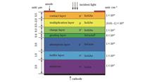
Results and Discussions With the device simulation tool Silvaco-TCAD, the impact of the doping concentration and thickness of the multiplication layer on the internal electric field intensity, current characteristics, and capacitance characteristics of avalanche photodetector is investigated in detail. Fig. 5(a) and Fig. 8(a) suggest that an increase in the doping concentration of the multiplication layer will lead to the rising peak electric field intensity in the multiplication layer and capacitance, respectively. Meanwhile, Fig. 5(b) and Fig. 8(b) indicate that the electric field intensity and the capacitance of the device decrease with the increase in the thickness of the multiplication layer. Further research suggests that the punch-through voltage of the device turns up linearly with the increase in the thickness of the multiplication layer, and the breakdown voltage turns down first and then up before the thickness of 1.0 μm [Fig. 7(b)]. However, the increase in the doping concentration of the multiplication layer causes a decrease in the breakdown voltage of the device, while the punch-through voltage essentially remains unchanged [Fig. 6(b)]. In addition, the variation of punch-through voltage and breakdown voltage is explained by the combination of the electric field distribution and the multiplication factor.ObjectiveAvalanche photodetectors with inner multiplication gain have greater sensitivity than PIN photodetectors without altering the signal characteristics, which is more suitable for application in optical communication and other related fields. Among them, the separation of absorption, multiplication, and charge layer structure of InGaAs avalanche photodetectors are extensively studied. Through the reasonable design of multiplication layer structure parameters, the high electric field in the multiplication layer and low electric field in the absorption layer can be regulated by the charge layer at the same time, which results in a better multiplication effect in the multiplication layer and inhibits current generated in the absorption layer. In addition, the ternary compound In0.83Al0.17As has higher carrier ionization rate and electron mobility than InP, so it has greater benefits as the multiplication layer for avalanche photodetectors. However, there are few reviews on the effect of the doping concentration and thickness of the multiplication layer on the device performance. To deeply explore the variation rule of avalanche photodetectors in linear mode and elaborate on the impact of the multiplication layer parameters on the device photoelectric performance, this paper studies the doping concentration and thickness of the multiplication layer of In0.83Ga0.17As/GaAs avalanche photodetector in detail. It aims to explore the influence of different doping concentrations and thicknesses of the multiplication layer on the current characteristics, electric field intensity, and capacitance of the device, and research the relationship of the punch-through voltage and breakdown voltage of the device with the doping concentration and thickness of the multiplication layer. It is of great significance to discover the working mechanism of the device in linear mode.MethodsIn this study, the effect of the In0.83Al0.17As multiplication layer on the overall performance of In0.83Ga0.17As/GaAs avalanche photodetector is researched with a device simulation tool Silvaco-TCAD. Firstly, the physical models related to conmob, fldmob, auger, srh, bgn, bbt, optr, and impact selb have been applied to define the material parameters of each layer of the device. The energy band and electric field distribution of the device are simulated, which suggests that the device meets the prerequisites of avalanche multiplication and explains the avalanche multiplication process. Secondly, the I-V characteristics of the device in dark and light conditions are simulated. Finally, the effects of the doping concentration and thickness of the multiplication layer on the internal electric field distribution, the punch-through voltage and breakdown voltage, and the traits of the alternating current small signal are simulated. In addition, the combination of electric field distribution and multiplication factor is utilized to explain the variation of punch-through voltage and breakdown voltage.ConclusionsIn this study, the impact of the doping concentration and thickness of the multiplication layer on the electric field intensity, current characteristics, and capacitance characteristics of In0.83Ga0.17As/GaAs avalanche photodetector is explored in detail. The results exhibit that with the thickness of the multiplication layer increasing from 0.5 μm to 2.0 μm, the peak electric field intensity and capacitance decline from 4.9×10⁵ V/cm and 1.4×10⁻¹⁵ F/μm to 4.1×10⁵ V/cm and 0.6×10⁻¹⁵ F/μm, respectively. In addition, the rise in the doping concentration of the multiplication layer causes an increase in the capacitance and the peak electric field intensity in the multiplication layer. When the doping concentration of the multiplication layer is 1×1016 cm-3, the values are 1.4×10⁻¹⁵ F/μm and 5.6×10⁵ V/cm, respectively. Further research shows that with the increment in the thickness of the multiplication layer, the punch-through voltage of the device increases linearly, while the breakdown voltage at the thickness of 0.5 μm, 1.0 μm, 1.5 μm, and 2.0 μm is 50 V, 44 V, 47 V, and 55 V, respectively, which decreases first and then increases. However, a higher doping concentration of the multiplication layer will lead to a lower breakdown voltage of the device. This study is of great significance for the working mechanism of In0.83Ga0.17As/GaAs avalanche photodetector in linear mode and the application of high-speed transmission in the future.
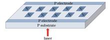
Results and Discussions We have discovered that there is a crosstalk phenomenon in pixels far from the irradiation area in the experiment of a 512×1 linear HgCdTe array detector irradiated by a pulsed laser. COMSOL Multiphysics finite element simulation software is used to simulate the carrier concentration distribution in the chip (Fig. 7) and the change of carrier concentration in the center of each pixel with the laser irradiation time (Fig. 8) to study the mechanism of the device's crosstalk phenomenon. It is discovered that the crosstalk of pixels close to the irradiation area is directly caused by the lateral diffusion of photogenerated carriers along the array alignment, while it has little effect on pixels far from the irradiation area. By simulating the direction of the electric field in the chip (Fig. 9) and the common electrode voltage (Fig. 10), the reason for the response of pixels far from the irradiation area can be fundamentally explained. It is discovered that some photogenerated carriers move to the common electrode under the action of the electric field, which results in the decrease in the common electrode voltage and the rise in all pixels' responses. The measure of trench isolation to suppress crosstalk (Fig. 11) is established based on the understanding of the device's electrical crosstalk generation mechanism, and simulation results (Fig. 12) show that the measure has significantly suppressed electrical crosstalk.ObjectiveThe crosstalk effect has always been one of the challenging issues in detector performance. Due to the increase in the detector array scale and the decrease in pixel center distance, the spatial resolution of the detectors greatly improves, and the crosstalk effect becomes more obvious, with a significant impact on the performance of the detectors. The crosstalk effect considers the problem of signals produced in the target pixel being interfered by some factors and makes other pixels to produce response signals. Crosstalk can be divided into optical crosstalk and electrical crosstalk based on different generation mechanisms. Optical crosstalk refers to the optical factors such as light reflection, refraction, and diffraction that make signals appear in other pixels. Electrical crosstalk refers to the signal response of other pixels due to the diffusion of photogenerated carriers. HgCdTe detector is widely used in both civil and military fields because of its high sensitivity, broad coverage band range, and other advantages. The crosstalk phenomenon exists in array HgCdTe detectors under continuous laser or pulsed laser irradiation, according to a lot of recent studies on the laser irradiation effect of HgCdTe array detectors. Previous research has shown that optical crosstalk is not the primary mechanism driving the response of unirradiated pixels in array devices, and it is inferred that this response is caused by electrical crosstalk. However, the conclusion has not been verified systematically. In this study, a linear HgCdTe array detector is used as the research subject, and we try to explore the mechanism and degree of electrical crosstalk as well as practical strategies for reducing it. In addition, we expect that these findings can have a certain reference value for improving the performance of detectors.MethodsWe use COMSOL Multiphysics finite element simulation software to establish a three-dimensional simulation model of a pulsed laser irradiation detector chip and study the crosstalk problem in a laser irradiation linear HgCdTe array detector experiment. Firstly, on the basis of the mechanism of electrical crosstalk caused by the diffusion of photogenerated carriers, the distribution of carrier concentration in the chip under laser irradiation with different energy densities is simulated. It is discovered that the diffusion of photogenerated carriers has a slight direct impact on pixels that are far from the irradiation area. Secondly, the direction of the electric field in the chip is simulated during laser irradiation, and it is discovered that the electric field under laser irradiation points to the common electrode. This electric field will make some photogenerated carriers to move to the common electrode, which will change its voltage and affect the output of the detector. Additionally, the common electrode voltage of the chip is simulated under different energies of laser irradiation, which confirms the conclusion that a decrease in the common electrode voltage can result in a response from every pixel of the detector. Finally, a measure to suppress the crosstalk is suggested. In other words, a three-dimensional isolation trench is designed based on the principle of limiting or reducing the lateral diffusion of photogenerated carriers, and the effect of the suppression of crosstalk is verified by simulation.ConclusionsIn view of the crosstalk phenomenon in the laser irradiation linear HgCdTe array detector experiment, the mechanism of the crosstalk is revealed by simulating the carrier concentration distribution, photocurrent, electric field direction, and common electrode voltage in the laser irradiation photosensitive chip in this paper. Research shows that the lateral diffusion of photogenerated carriers along the array alignment directly contributes to the crosstalk of pixels close to the irradiation area, while it has little effect on pixels far from the irradiation area. There is an electric field pointing to the common electrode of chip when it is irradiated by the laser. Under the influence of this electric field, some photogenerated carriers move to the common electrode, which results in the voltage reduction of the common electrode, and then all of the detector's pixels rise in response. In addition, the measure of electrical crosstalk suppression by trench isolation, which has a significant influence on crosstalk suppression, is proposed based on the mechanism of electrical crosstalk generated by the lateral diffusion of carriers. The problem of crosstalk brought by the common electrode voltage variation can be resolved by changing the circuit design or correcting the output signal. It is necessary to conduct more research on the specific measures.
Results and Discussions In a triple-carrier 128 GBaud polarization multiplexing hexadecimal quadrature amplitude modulation (PM-16QAM) FTN wavelength division multiplexing (WDM) system, a back-to-back and fiber transmission simulation platform is constructed to comprehensively investigate the performance of the proposed scheme.The simulation results demonstrate that the proposed scheme can effectively perform high-precision fine FOE based on the rough FOE results (Fig. 5). When the CZT search range is f1-100 MHz-f1+100 MHz, the FOE range of the proposed scheme is about -18-18 GHz, which means the estimation accuracy is significantly improved compared with the 1024-point 4th-FFT algorithm [Fig. 6(a)]. When the acceleration factors are 0.95, 0.90, and 0.85, the residual frequency offsets of the proposed method are about 2, 2.5, and 3 MHz, respectively [Fig. 6(b)], and the optical signal-to-noise ratio (OSNR) tolerances of the system using the proposed scheme are 23.5 dB, 23.8 dB, and 24.5 dB, respectively under the soft-decision forward error correction (SD-FEC) threshold at the bit error rate (BER) of 2×10⁻² (Fig. 7).The experimental results show that the absolute value of the maximum FOE error of the proposed method is about 2 MHz and 3 MHz when the acceleration factors are 1 and 0.9 [Fig. 9(a)]. Additionally, the proposed scheme can achieve a stable FOE in the -8-8 GHz frequency offset range, and the estimation accuracy is higher than that of the 512-point 4th-FFT algorithm [Fig. 9(b)]. When the acceleration factors are 1 and 0.9, the OSNR tolerance of the system using the proposed scheme is 19 dB and 20 dB respectively under the SD-FEC threshold at BER of 2×10⁻² (Fig. 10).Compared with the traditional blind FOE algorithm based on 4th-FFT, the overall computational complexity of the proposed scheme is significantly reduced, which is about 8% of the conventional algorithm, under similar estimation accuracy (Table 1).ObjectiveIn virtue of the computing power provided by advanced digital signal processing (DSP) technology, the faster-than-Nyquist (FTN) optical transmission technology can compensate for impairments, which has recently been considered a potential approach in the field of large-capacity coherent optical transmission. However, the severe inter-symbol interference (ISI) caused by tight FTN filtering will lead to the heavy deterioration of accuracy and stability in frequency offset estimation (FOE), which needs to be combated to guarantee the system performance. At present, the 4th fast Fourier transform (4th-FFT) algorithm is usually used for FOE in FTN coherent optical systems. To obtain a more ideal estimation accuracy, the 4th-FFT algorithm requires a large number of estimated samples to obtain a high-resolution FFT spectrum, which will bring greater computational complexity. Thus, the conventional FOE algorithm in the DSP module of the receiver is faced with conflicting effectiveness and complexity, which significantly degrades the stability and accuracy of FOE. Aiming at the above problems, this paper proposes a two-stage FOE algorithm based on phase difference of training sequence and chirp Z-transform (CZT) for dual-polarization (DP) 16QAM FTN-WDM systems.MethodsThis paper puts forward a two-stage FOE algorithm. In the first stage of the proposed scheme, the periodic multi-symbol structure of the training sequence is adopted to process multiple inter- and intra-period averaging to alleviate the influence of the noise on FOE, which can achieve stably rough FOE with low overhead. In the second stage, according to the rough frequency offset value f1 in the first stage, the CZT spectrum search range is set and the starting and ending frequency points (the lower and upper limit values of the FOE range) are determined. Specifically, with the rough frequency offset value f1 as the center point, the spectrum search of equal length is carried out to both sides respectively. According to the starting and ending frequency points and the preset frequency resolution (i.e., the accuracy of CZT-based FOE), the number of output sequence points of CZT is determined. Then, CZT is performed based on the number of the points on the received signal after the 4th power operation to obtain the CZT spectral function, and the maximum spectral line value of the CZT spectral function is extracted. Through the maximum spectral line value and the CZT spectrum search range, the fine frequency offset value f2 can be obtained. Thus, the high-precision FOE can be completed with low computational complexity while ensuring estimation accuracy.ConclusionsAiming at the requirement of the FTN system for low complexity, high precision, and high-reliability FOE algorithm, this paper proposes a two-stage FOE algorithm based on training sequence and CZT. The simulation results of the 128 GBaud PM-16QAM FTN-WDM system show that when the acceleration factors are 0.95, 0.90, and 0.85, the residual frequency offsets of the proposed scheme are about 2, 2.5, and 3 MHz in the carrier frequency offset range of -1.6-1.6 GHz. Under the typical 1 GHz frequency offset, the OSNR tolerances at BER of 2×10⁻² are 23.5 dB, 23.8 dB, and 24.5 dB respectively. The computational complexity of the proposed scheme is reduced by 92% compared with the 4th-FFT algorithm of the same precision. The 40 GBaud PM-16QAM FTN-WDM offline experimental results show that when the acceleration factor is 0.9, the absolute value of the maximum FOE error in the frequency offset range of -1.6-1.6 GHz is about 3 MHz. Thus, the excellent performance and outstanding advantages of the proposed scheme make it a preferable candidate for the FOE of DP-16QAM signal in practical FTN-WDM systems.
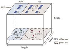
Results and Discussions To verify the proposed scheme, a typical office scenario is set up for simulation, where 9 LEDs are distributed on the ceiling of an indoor room. 3 LEDs are located above the office area and the rest are arranged in the public area. The average emission power of each LED is 1 W. Without loss of generalization, two legitimate users are assumed in the office area, and an unknown number of eavesdroppers randomly appear anywhere in the public area. Both legitimate users and eavesdroppers are located on a horizontal receiving plane of 0.5 m from the ground. The other parameters are given in Table 1. Simulation results show that the maximum value of the SINR of the eavesdropper in the public area is -17.22 dB when using the proposed cooperative jamming scheme (Table 2), which represents SINR of the eavesdropper in the worst case. Compared with the artificial noise-based precoding and spatial jamming schemes, the SINR of the eavesdropper decreases by 11.73 dB and 24.30 dB in the worst case, respectively (Table 2), and the SINR of the eavesdropper is lower than the traditional two schemes in the whole public area (Fig. 5). At the same time, the minimum value of the secrecy sum-rate of the system is increased by 0.39 bit·s-1·Hz-1 and 0.78 bit·s-1·Hz-1, respectively (Fig. 6). This shows that the proposed scheme outperforms the traditional two schemes when the optimization objective is to minimize the eavesdropper's SINR in the worst case. Through the joint optimization and design, the jamming signals will disturb the eavesdropper's reception to the maximum extent without affecting the legitimate user's reception.ObjectiveVisible light communication (VLC) has received extensive attention in recent years owing to its numerous advantages such as abundant spectrum resources, immunity to electromagnetic interference, low cost, etc. Due to the inherent broadcast characteristics of VLC, VLC channels are inevitably susceptible to eavesdropping by potential unauthorized users who are inside the same open area illuminated by the light-emitting diode (LED) transmitters. Therefore, security of VLC systems has become an issue of critical importance and substantial efforts have been devoted to it. Among the existing security methods, physical layer security (PLS) schemes have been applied to enhance the overall system security by complementing existing cryptography-based security techniques of upper layers. PLS techniques use channel characteristics and physical-layer features (such as multi-antenna and cooperative nodes) to reduce the attained information at the eavesdroppers. Artificial noise has been emerged as a promising technique to improve the security of multi-user multiple-input multiple-output (MISO) VLC systems. Artificial noise will disturb the eavesdroppers' reception without affecting the legitimate users' signals. Most of researches on artificial noise assume a single legitimate user with an eavesdropper of unknown location, and do not consider the realistic scenarios where multiple legitimate users and multiple eavesdroppers with random locations exist. Such scenarios are common in indoor workplaces including government offices, banks, etc. To enhance the security performance under the above typical scenarios, this paper proposes an artificial noise generation scheme based on cooperative jamming to minimize the signal to interference plus noise ratio (SINR) of the eavesdropper in the worst case and improve the security performance of the VLC system.MethodsIn a MISO visible light communication system, an artificial noise generation scheme based on cooperative jamming is proposed to improve the security performance of the system when unknown number of eavesdroppers may appear anywhere in the public area. In the proposed scheme, the signal source LEDs in the legitimate user's area jointly send jamming signals with the LEDs in the public area. Through the joint design of the jammers in the two areas, the effect of the jamming signals on the legitimate user's reception can be cancelled to zero. On this basis, we formulate an optimization problem to minimize the SINR of the eavesdropper in the worst case, and use the concave-convex process (CCP) to find the optimal solution. Through the joint optimization and design of the jammers, the generated jamming signals will disturb the eavesdropper's reception to the greatest extent without affecting the legitimate users' signals, thus enhancing the secrecy sum-rate and security performance of the system.ConclusionsThis paper studies the physical layer security of MISO VLC systems under typical indoor office scenarios. When users and eavesdroppers are located in different areas and the number and location of eavesdroppers are random, a cooperative jamming method is proposed to generate artificial noise. On one hand, the LEDs in the office area send confidential signals required by legitimate users. On the other hand, the LEDs in the office area jointly send jamming signals with the LEDs in the public area. Through the joint optimization and design of the jammers in different areas, the jamming signals will minimize eavesdropper's SINR in the worst case without affecting the communication quality of legitimate users. Simulation results show that compared with the artificial noise-based precoding and spatial jamming schemes, the proposed cooperative jamming scheme reduces the eavesdropper's SINR in the worst case by 11.73 dB and 24.30 dB, respectively. The secrecy sum-rate has been significantly improved, thereby improving the security of the system.
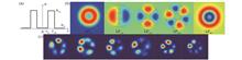
Results and Discussions In the simulation, the first eight modes (LP01, LP11e, LP11o, LP21e, LP21o, LP31e, LP31o, and LP02) that support the selected RCF are used as examples with a wavelength of 1550 nm. Four mode-superposition cases (superposition of the first three, five, seven, and eight modes) are analyzed to test the performance of the PFCNN-MD. By comparing the PFCNN-MD with traditional VGG-MD schemes without pre-training, it can be found that even in the three-mode case, the loss function in the VGG-MD always oscillates at higher loss values and cannot converge, while that in the PFCNN-MD quickly converges to 0.007 (Fig. 3). Moreover, the designed PFCNN architecture can achieve convergence within about 55 epochs of training in the four mode superposition cases. The error results of ρ2 and θ in the superposition case with three to eight modes are compared between the non-pre-trained PFCNN-MD and the VGG-MD pre-trained on the ImageNet dataset. It can be found that in the eight-mode case, compared with that by VGG-MD, the error of ρ2 is reduced from 5.62% to 0.95%, and the accuracy is improved by more than five times. The error of θ drops from 11.86% to 1.92%, and the accuracy is improved by about eight times (Fig. 4). In the three-mode case, the average correlation coefficient between the reconstructed beam pattern and the original beam pattern reaches 99.99%, and one MD consumes 5 ms. When the mode number becomes eight, the average correlation remains at 99.60%, and the trained CNN completes one MD in only 9 ms (Fig. 5). In order to further characterize the performance of PFCNN-MD, the proposed method is compared with four CNN-MD methods (VGG, NFFL-CNN, DH-ResNet18, and DenseNet121) emerging in recent years on various indexes (Table 1). In the eight-mode case, even if the RCF has more complex modal coupling characteristics, the accuracy of the PFCNN is still higher than that of other CNN-MD schemes in the step-index FMF. The time consumed by PFCNN to perform one MD is on the order of ms. In addition, the PFCNN-MD doesn't require the pre-training process and only needs a near-field (NF) beam pattern for training and algorithm input. It has lower experimental operation complexity and equipment requirements. Much time for pre-training is also saved. Moreover, the PFCNN only uses a single GPU to achieve more accurate MD, saving many computer computing resources and reducing energy consumption. Although PFCNN needs to go through about 55 epochs of training to converge the network, it can complete in advance. In the experiment, an experimental setup based on an all-fiber device is used to collect real beam pattern to examine the practical performance of the PFCNN. The average correlation coefficient between the real and reconstructed patterns in the test dataset is 90.01% (Fig. 7).ObjectiveThe core of a ring-core few-mode fiber (RCF) is composed of a central refractive index (RI) depression region and an outer high RI ring. The RCF plays an important role in modal gain equalization, mode division multiplexing transmission, and vortex beam generation. In order to figure out the mode coupling and reveal the associated beam properties in few-mode fibers (FMFs), the mode decomposition (MD) techniques are required, which can obtain the modal weight (ρ2) and modal relative phase difference (θ) from modal superposition images. However, the RCF has complex modal overlap and mode coupling because the power of each mode is confined to the same high RI ring region. As a result, the mode coupling analysis of RCFs faces severe challenges. In this paper, we propose a pretraining-free CNN-MD algorithm (PFCNN-MD) based on a convolutional neural network (CNN) for high-accuracy characterization of complex couplings in RCFs, and the algorithm uses branch structures with different receptive fields to improve the learning ability of neural networks.MethodsIn the PFCNN-MD, the normalized field distribution of each supported mode is calculated based on the tested RCF's structural parameters first. After that, massive simulated grayscale beam patterns can be generated numerically with random modal coefficients as the dataset. The corresponding modal coefficient values are set as the label. The generated beam pattern dataset is divided into three parts: training set, validation set, and test set. The CNN is trained by using the training set, which helps the neural network learn the modal features from the beam patterns. During the training process, the training set is iteratively input into the network. The weight and bias parameters of the CNN are updated by minimizing the difference between the network output and the label until the CNN converges. The validation set is used to monitor network fitting and tune network hyperparameters. After the trained CNN has been examined for generalization based on the test set, MD can be implemented on the real beam pattern. The entire process can be completed with only one forward propagation calculation by the trained CNN. The designed PFCNN-MD architecture consists of eight blocks (Fig. 2). In blocks 3 to 7, the InceptionNet-type branch structures are set to increase the width and depth of the network. A variety of small-sized convolution kernels and pooling layers are combined on each branch to extract features in parallel. This not only enables the neural network to have a strong learning ability for features of different scales but also effectively avoids the defects of overfitting and inefficient use of computing resources. Therefore, the designed CNN structure does not require pre-training to enhance the network's ability. Instead, the extraction of complex modal features can be realized directly on the beam pattern training set.ConclusionsIn this paper, a high-precision PFCNN-MD algorithm is proposed to solve the problem of complex mode coupling characterizing in the RCF. The proposed algorithm can fast complete the training and obtain high-precision MD results without pre-training. The performance of PFCNN-MD is tested from both simulation and experiment. In the simulation, compared with that by the traditional CNN-MD, errors of ρ2 and θ in the eight-mode case are lower than 0.95% and 1.92%, which are decreased by 80% and 87.5%, respectively. One MD consumes 9 ms. In the experiment, the correlation between the real and the reconstructed beam patterns is higher than 90%. The PFCNN-MD algorithm shows great potential in real-time MD and the characterization of the RCF's mode coupling properties.
Results and Discussions To verify the validity of the simulation analysis, we build an experimental setup (Fig. 6) and conduct experiments on the capture and capture stability of Chlorella cells by using optical tweezers. The 980 nm SMF is connected to a laser source with a wavelength of 980 nm as the input, and the 1550 nm SMF is immersed in the Chlorella cell solution as the output. When the laser is turned on, the Chlorella cells in the effective trap area of the optical fiber probe are attracted to the fiber tip. Due to the stronger light field gradient distribution on both sides of the fiber tip, the Chlorella cells are trapped on both sides of the fiber tip (Fig. 7). The experimental results show that the optical tweezer structure is able to simultaneously trap multiple Chlorella cells in three directions and form a biological chain. The capture remains stable when the fiber moves at a speed of about 14 μm/s (Fig. 9).ObjectiveCurrently, some biophotonic devices or cell-to-cell interactions and communications require the capture of particles, especially multiple particles. Since the invention of optical tweezers in 1986, optical tweezers have become an important tool that is widely used in the manipulation and study of cells, viruses, atoms, colloids, and other particles. Based on conventional optical tweezers, multi-directional alignment of multiple particles is achieved by various methods such as holographic optical tweezers, single beam before helical phase, and optical binding. However, these techniques require bulky optical components, which complicates optical tweezer systems and hinders operational flexibility. To overcome the shortcomings of conventional optical tweezers in capturing multiple particles, researchers have used optical tweezers to capture multiple particles. Some researchers have created multiple optical traps using dual fibers, which enables the capture of multiple particles in two and three dimensions, and they have manipulated, deflected, and stretched multiple cells using two misaligned single-mode fibers. Some researchers have used multicore fibers for two-dimensional optical interference capture of multiple particles and Escherichila coli cells manipulation of multiple particles using photonic crystal mode multiplexing, while others have used fiber traps and photothermal effects to manipulate a large number of particles. However, the optical fiber probes in the above methods with multi-core fibers and photonic crystals are, in general, structurally complex, and difficult to replicate. Focusing on the complex structure of multi-core fiber and photonic crystal fiber probe, this paper proposes a single-fiber optical tweezer structure with two modes being composite. The structure utilizes two different modes of fiber staggered splicing to ensure the LP01 and LP11 modes coexist in the output optical field, and the two modes of the beam have different focused optical fields to achieve the capture of multiple Chlorella cells in different directions. The captured Chlorella cells act as lenses to refocus the beam to capture the next cell and then form multiple biological chains.MethodsIn order to make LP01 and LP11 mode beams coexist in the fiber, 980 nm single mode fiber (SMF) and 1550 nm SMF are utilized for splicing (Fig. 1). The energy ratio of the LP01 and LP11 mode beams is also controlled by controlling the offset of the two fiber splices, which in turn ensures that each optical trap can have sufficient optical power to trap particles. In order to analyze the focused optical field characteristics of the composite mode fiber, a two-dimensional model based on finite element analysis is developed using simulation software. The output optical field distribution of the composite fiber with 980 nm SMF and 1550 nm SMF staggered by 2 μm is simulated, and the optical radiation pressure applied to Chlorella cells is calculated. The simulation results show that the LP01 mode beam is focused at the tip of the fiber probe and forms an optical potential well [Fig. 4 (a)]. The LP11 mode has a completely different light field at the tip of the fiber probe [Fig. 4 (b)]. The LP11 mode light field is not concentrated near the optical axis. The convergence position of the LP11 mode beam is inside the fiber tip. Due to the special fiber shape, the light field gradient distribution on the side of the fiber is large, so Chlorella cells outside the fiber tip will be attracted and move toward the fiber tip and eventually be captured. The coexistence of the LP01 and LP11 mode beams integrates the characteristics of both LP01 and LP11 mode beams [Fig. 4 (c)]. The LP01 mode beam is also present while the LP11 mode beam is excited in the fiber, and the two-mode beams exhibit different focused light fields because they have different propagation constants. In other words, the LP01 and LP11 modes produce different stable capture points when passing through the same fiber probe. When LP01 and LP11 modes coexist, the simulation results show that Chlorella cells are captured on both sides of the optical axis and the fiber tip, respectively (Fig. 5).ConclusionsIn summary, a single-fiber optical tweezer for multiplexed alignment of multi-biological cells is proposed in this paper. The optical tweezer utilizes two different modes of fiber staggered splicing to make LP01 and LP11 modes coexist in the output optical field. Since the two mode beams have different propagation constants and exhibit different focused light fields, the capture of multi-biological cells in different directions can be achieved. Through the finite element analysis method, the optical field distribution of the optical fiber tweezer with 980 nm SMF and 1550 nm SMF being composite is simulated, and the force on Chlorella cells is analyzed. Finally, it is shown that the optical tweezer can capture multiple Chlorella cells simultaneously in three directions and form a biological chain. The capture remains stable when the fiber travels at a speed of about 14 μm/s. The simple structure of this optical fiber tweezer provides more possibilities for biosensing and direct detection of biosignals.
ObjectiveThe imaging process of polarization images in the natural environment is easily affected by noise, which not only causes the acquired relevant polarimetric parameters to deviate from their real values but also affects the further processing of subsequent polarization information. Due to nonlinear operations, polarimetric parameters such as the degree of polarization (DoP) and the angle of polarization (AoP) are easily distorted by noise, especially in photon-starved environments. Therefore, effective denoising is crucial to polarimetric imaging. The denoising method based on deep learning can significantly remove the influence of noise on polarization images. However, the performance of current supervised algorithms is highly dependent on the labeled dataset, and high-quality polarization labels are difficult to obtain in practical applications, which limits the application of the existing methods. Therefore, this paper proposes a polarization image denoising method based on unsupervised learning. This method breaks the restriction that supervised learning-based deep learning requires strictly paired images and uses unpaired polarization images to train a polarization-specialized cycle generative adversarial network (CycleGan). The method in this paper are of great significance to the application of polarimetric imaging in complex noise environments.MethodsIn the proposed CycleGan structure, the discriminator for the input domain is removed, and two discriminators for polarimetric parameters are added. In the structure of generators, the residual dense block (RDB) is introduced to extract abundant local features via densely connected convolutional layers, and PatchGANs are adopted for discriminators, which can work on arbitrarily sized images and grow the receptive field after each convolution layer. In addition, a batch normalization (BN) layer and a ReLU layer are added right after each convolutional layer to accelerate network training. Furthermore, a cycle consistency loss is maintained to keep the consistency between input and output, and two cycle gradient losses are introduced for the degree of linear polarization (DoLP) and AoP to preserve the variations of polarization information. With the help of the designed network structure and the polarization-based loss function, the network trained by unpaired polarization images can statistically learn the mapping between noisy and clean images.Results and DiscussionsExperiments show that the network can effectively suppress the noise of polarization images in different indoor and outdoor environments and recover DoLP and AoP. The ablation experiment proves the effectiveness of additional polarization discriminators. With two discriminators, the network accurately recovers both DoLP and AoP images (Fig. 3) and achieves the highest PSNR/SSIM value among different network structures (Table 1). Compared with other methods, the unsupervised method has the best performance in terms of intensity, DoLP, and AoP images (Fig. 4). The average PSNR and SSIM of indoor images illustrate that the method has advantages in the reconstruction of DoLP images (Table 2). Several groups of experiments on different materials, including resin, fabric, wood, and plastic, are conducted to verify the universality of the proposed method. The denoised results reveal that the proposed method can suppress the noise of these materials for polarization information (Fig. 5). Finally, experiments with outdoor noise polarization images are carried out to verify the robustness of the method. Compared to the supervised method, the unsupervised method does not see dramatical performance degradation when applied to different environments (Fig. 6), which is important for the application of polarization imaging in realistic environments.ConclusionsThis paper proposes a polarization image denoising method based on unsupervised learning. On the basis of the CycleGan model, a structure of generative adversarial network suitable for polarization image denoising is designed. Through an unsupervised training network with unpaired images, a denoising network model that can effectively remove the noise of polarization images and restore polarization information is obtained. Experiments with indoor images are conducted to test the method, and qualitative and quantitative evaluations are given. The experimental results show that this method can achieve the same performance as the supervised learning method in indoor image denoising and can effectively restore polarization information, especially in DoLP image restoration. Furthermore, the polarization images of different materials are tested. The results reveal that this method has good generalization and can effectively recover the polarization information of different materials. In addition, the outdoor images are also tested, and a qualitative evaluation is presented. The experimental results suggest that this method can effectively remove the noise of indoor and outdoor images and restore real polarization information when indoor images are used as the training set. The models and methods proposed in this study can be extended to other applications. For example, they can be used to study polarization image denoising and polarization information recovery in extreme environments (e.g., night, low light).
Results and Discussions After the final image is obtained by the platform, PSF is used to evaluate the quality of the final image, and the imaging results are compared with the simulation results [Fig. 7(c)] and the results of model of ideal MLAs [Fig. 10(d)]. The FWHM value of the ideal PSF curve [the dot-and-dash line in Fig. 10(d)] without considering the errors is 51.72 μm, and that of the simulated PSF curve (the solid line) with the error added is 75.35 μm. The FWHM value of the PSF curve (the dotted line) measured experimentally is 84.77 μm. Therefore, compared with the model of ideal MLAs, the model of MLAs considering the errors is more accurate, and the error of the measurement result compared to simulation result is about 12%. The reason is that the model of ideal MLAs cannot fully consider the actual imaging situation, and its interference factors are fewer. Therefore, the imaging result is better than the actual one, and the FWHM value is smaller.ObjectiveTo study the influencing factors of imaging quality of microlens arrays (MLAs), this paper conducts optical simulations and experiments to establish the relationship between lens errors and optical imaging quality of MLAs. The results can provide a theoretical basis and guidance for the establishment of function-driven ultra-precision machining technology for optical MLAs. The methods for preparing MLAs can be divided into direct and indirect methods considering the necessity of making masks or molds with three-dimensional concave structures. In any case, the manufacturing errors will eventually be mapped onto the lenses and have an impact on the optical performance of the lenses. Most published studies on the imaging simulation of MLAs do not consider the impact of errors on imaging performance. Meanwhile, the image obtained by MLAs, falling within indirect computational imaging, is the calculation result based on the information received from the sensor. The existing studies on the optical performance measurement of MLAs, however, mainly analyze the image information directly received from the sensor. Therefore, for the MLAs produced by the slow tool servo diamond turning and the UV light curing process, a simulation model of optical MLAs is developed in the optical software Zemax, and the lens errors are introduced into the simulation of imaging performance. In this paper, the errors include the depth error and curvature radius error of the lens unit, as well as the error of the entrance pupil diameter. Moreover, a platform for the optical performance measurement of MLAs is established to test the imaging performance of MLAs, which applies the calculated final imaging results for imaging quality evaluation. Finally, the accuracy of the simulation model is verified by the comparison of the simulation and experimental results.MethodsBoth simulation and experiments are applied in this study. Zemax is the optical design software of Zemax Development Corporation of the United States. It can calculate the point spread function (PSF) curve of the current optical system, and the imaging quality can be evaluated according to the full width at half maximum (FWHM) of the PSF curve. A smaller FWHM indicates a smaller degree of spot dispersion and better imaging quality. The construction of the simulation model of optical MLAs includes the following steps. Firstly, the test optical path should be set. A single-wavelength (0.656 μm) parallel light reaches the image sensor after passing through the MLAs. At this time, each lens unit forms an image, which is a diffuse spot that will be received by the image sensor. The image sensor is set at a predetermined focal distance, namely, the effective focal length of the ideal lens unit (30.66 mm). Secondly, according to the test optical path, the model of ideal MLAs is built by Zemax. Thirdly, the image formed by each lens unit is calculated, and the original light field image and the final image are obtained, where the latter is obtained with the pixel rearrangement method (Fig. 2). At this time, the final image is still a diffuse spot, and hence, the PSF curve of the final image and its FWHM can be generated by the light intensity distribution of the spot. Similarly, after measurement, the errors of actual MLAs are added to the model of ideal MLAs, and its PSF curve as well as the FWHM of the curve can be generated. A platform for the optical performance measurement of MLAs is established (Fig. 8) to verify the accuracy of the simulation model of optical MLAs and form a performance detection system for optical MLA elements. The test optical path of the detection platform is the same as above. The test platform can measure the focal length of each lens unit of MLAs, and the measurement results are compared with the simulation results (Table 5) to verify the model of optical MLAs upon the addition of errors. After that, the light field imaging system for MLAs is established. The position and size of the focal spot are measured, and the quality of the final image of the MLAs is evaluated by the PSF curve and its FWHM.ConclusionsIn this paper, a simulation method based on Zemax for MLAs is proposed. The related errors of lens units (the curvature radius error, entrance pupil diameter, lens depth error, and surface irregularity error) are measured. According to the measurement results, a simulation model of MLAs considering the errors is built. Compared with the model of ideal MLAs that does not consider lens errors, the simulation model built in this paper is more accurate. In addition, a platform for the optical performance measurement of MLAs established in this paper can be used as an evaluation and measurement tool for the imaging results of MLAs. The platform can detect the imaging quality of MLAs and evaluate the final imaging result. The focal-spot size and position errors of each lens unit are measured, and the standard deviation of focal length measurement is about 0.12 mm. The PSF curve is used to evaluate the quality of the final imaging results. Compared with the simulation, the FWHM error is about 12%. To sum up, through simulation and measurement, the relationship between the lens error of MLAs and the optical imaging quality is established, which can provide guidance and suggestions for the manufacturing of MLAs.
Results and Discussions After the system is built, and the initial calibration is completed, Soleil-Babinet compensator is regarded as a standard sample to be determined. Adjust the displacement of the optical wedge of the compensator from 0 with an interval of about 0.02 mm, the signal amplitude is obtained by digital phase-locked technique, and the retardation and fast axis azimuth angle of the compensator are further solved. The calibration values of retardation are in good agreement with the measured values (Fig. 7), and there is a maximum relative error of 2.3% between the measured value and the calibrated value, which indicates that the measurement accuracy of retardation in this scheme. When the compensator displacement is at 0.500 mm, and the retardation is 151.118 nm, the maximum standard deviation is 0.032 nm, which indicates that the measurement repeatability and sensitivity of this scheme (Table 1). Stress birefringence experiment is carried out by using the BK7 glass specimen. The experimental results show that the stress retardation and birefringence are increased with the increase of the applied pressure (Fig. 8). When the applied pressure is 50.0 N, the standard deviation of stress birefringence is 0.17 nm/cm, which indicates that the measurement repeatability and sensitivity of the stress birefringence (Table 2). We also find that the stress retardation and birefringence of BK7 glass are not zero, when no pressure is applied at the beginning. The small retardation and birefringence values are 0.558 nm and 1.86 nm/cm respectively, which is induced during the production process. This is a defect that must be tested and evaluated in the optical element production. Moreover, the time interval of data measurement in the above experiments is set at 200 ms. The time can be set according to the actual situation via the FPGA digital phase-locked data processing cycle. In the application with no strict requirements on repeatability, the fastest data measurement rate can reach one data point each 10 ms.ObjectiveThe stress parameters of optical materials and optical components are important parameters to evaluate the mechanical strength, thermal stability, imaging quality and beam transmission quality of optical systems. During the growth of optical materials such as glass and optical crystal, structural stress will occur due to defects or physical and chemical changes. In the process of annealing and cooling, the uneven plastic deformation and uneven volume change caused by temperature change will produce residual stress. Cutting, grinding and polishing during the processing of components, as well as external forces during loading and clamping, will generate mechanical stress. When the stress is large, it is easy to cause the materials and components to explode. Even a small stress can cause poor refractive index and birefringence consistency, resulting in imaging distortion and astigmatism. Therefore, it is necessary for the development and production of high-performance optical system to measure the stress of optical materials and optical elements, and the stress should be controlled within the allowable range. Stress induced birefringence become the main index of stress defect evaluation in optical materials and components. Now, methods are applied to research the measurement of stress birefringence, such as polarization interference, polarization compensation, laser feedback, polarization modulation and polarization imaging. Nevertheless, measurement speed and accuracy still need to be further improved. For the needs of rapid and high-precision stress testing and evaluation of optical materials and optical components, a stress birefringence measurement scheme based on double cascaded photoelastic modulation with differential frequencies is proposed in this paper.MethodsConsidering the application advantages of photoelastic modulation, such as high modulation frequency, large optical aperture, high modulation purity and stable operation, a novel measurement method using photoelastic modulation is proposed. A simple polarimetry is constructed based on two photoelastic modulators with differential modulation frequencies. The stress birefringence retardation and fast axis azimuth angle are loaded into the differential frequency photoelastic modulation signals, and the digital phase-locked technology is used to extract the differential frequency signals and fundamental frequency signals of photoelastic modulation at the same time, so as to further solve the stress birefringence retardation and fast axis azimuth angle. The principle of the new scheme is analyzed, and an experimental system is built. The initial offset value of the system is calibrated experimentally without any sample. After that, the measurement accuracy and repeatability are measured by using a Soleil-Babinet compensator as standard sample. Finally, a BK7 glass specimen is loaded different stresses, and the measurement of stress birefringence is completed.ConclusionsIn present study, a novel stress birefringence measurement method based on differential frequency modulation with double photoelastic modulators is demonstrated. The principle of the new scheme is analyzed, and an experimental system is built. The initial offset value of the system is calibrated experimentally, and the measurement accuracy and repeatability are measured by using a Soleil-Babinet compensator, and the stress birefringence measurement for a BK7 glass specimen is carried out. The experimental results show that the accuracy of retardation measurement is 2.3%, the repeatability of retardation measurement is 0.032 nm, and the repeatability of birefringence measurement is 0.17 nm/cm. In addition, the measurement time of single data does not exceed 200 ms. Our study realizes simultaneous measurement of retardation and fast axis azimuth angle without any mechanical adjustment. This method has the application advantages of high measurement accuracy, high measurement repetition and fast measurement speed.
Results and Discussions First, the experimental results of the camera with the typical ordinary focal length (f=20 mm) show that the error of the calibration method employing the perspective projection is relatively lower (Fig. 4 and Fig. 5), which indicates that the perspective projection better describes the imaging process under the current configuration. In this case, the approximation error of the affine projection model cannot be negligible. Furthermore, the results demonstrate that the proposed calibration method is effective and reliable, and can be applied to ordinary cameras within a certain threshold. Additionally, the experimental results of the camera with typical telephoto lenses (f=100 mm) show that the calibration method of the telephoto camera based on the approximation projection model has better accuracy and robustness (Fig. 6 and Fig. 7), and the affine approximation projection model can be better adapted to the imaging process of telephoto cameras.As for actual experimental results, under the condition of ordinary focal length (f=35 mm) in Table 1, despite a small deviation, the calibration results of the Weak and Para methods under the affine approximation projection are still close to those of RML and RNML methods under the perspective projection model. This indicates that the calibration method under the perspective projection model can obtain higher precision results, and the approximation error of the affine projection model cannot be ignored. Further comparison of the calibration results of the Weak and Para methods shows that the two approximation models are basically equivalent under the current configuration. In the case of the telephoto camera (f=75 mm), the calibration parameters and image pairs acquired via the stereovision are applied to reconstruct the 3D planar template (Fig. 10). The out-of-plane error of the reconstructed plane is about 0.015 mm, which is significantly lower than the reconstruction error of methods under perspective projection, thus demonstrating the correctness and effectiveness of the proposed method.ObjectiveFeaturing unique advantages of high spatial resolution and more detailed information, telephoto cameras have been widely employed in military fields such as aerial reconnaissance, damage assessment, and patrol monitoring, as well as civil fields including industrial precision processing, aerial photogrammetry, deformation monitoring, and traffic surveillance. However, there are practical obstacles to the adoption of telephoto lenses on small-format cameras, with potential difficulties in self-calibration. A telephoto lens will inevitably narrow the field of view (FOV), exerting detrimental effects on the performance of the central perspective projection model, which will result in over-parameterization, ill-conditioning, and subsequent numerical instability in normal equations of the bundle adjustment. Linear dependencies between the intrinsic and extrinsic parameters make it rather difficult to recover satisfactory calibration parameters in such weak geometry conditions. Therefore, an alternative affine approximation of the perspective projection model is adopted to accommodate high-accuracy and close-range photogrammetry with telephoto lenses, which makes full use of the advantages of the model, such as high linearity, simplicity, and high robustness. Additionally, a calibration method of telephoto cameras based on the affine approximation projection model is proposed. By employing the proposed model, this paper aims to obtain better calibration performance of telephoto cameras, thereby laying a foundation for the application of telephoto cameras.MethodsAs the most common affine approximation of the perspective projection model, the characteristics of weak perspective and paraperspective projection are thoroughly elaborated, according to which a calibration method of telephoto camera based on the affine approximation projection model is built. In this paper, the formation mechanism of reversal ambiguity is thoroughly analyzed, and the estimation method of calibration parameters based on the planar template under the affine approximate projection is deduced in detail. First, combined with the normalized method on line-based homography estimation method and the partitioned regularization estimation algorithm, the homography between the image plane and the cooperative planar template can be obtained. Then, the initial values of the intrinsic and extrinsic parameters of the camera are calculated under the affine approximation projection model. With the minimum sum of the residual square of the re-projection image points under the perspective projection model as the cost function, a nonlinear optimization algorithm is adopted to refine the calibration parameters for minimizing the approximation error of the affine projection model. In addition, an additional stage with a control point is attached to the planar template to address pose ambiguity.ConclusionsA novel method of telephoto camera calibration based on the affine approximation projection model is proposed to address the over-parameterization of the perspective projection model in telephoto camera calibration. By the affine approximation projection model, the initial values of the calibration parameters can be obtained. Additionally, the method with the affine approximation projection model is more robust than that with the perspective projection model. With the minimum sum of the residual square of the re-projection image points under the perspective projection model as the cost function, a nonlinear optimization algorithm is adopted to refine the calibration parameters for minimizing the approximation error of the affine projection model. Besides, an additional stage with a control point is attached to the planar template to solve the pose ambiguity. Under the typical telephoto conditions where the angle of view is lower than 10? and the variation in the depth of the target along the line of sight is smaller than its average depth from the camera, the proposed method only requires the freely moving camera to observe a planar pattern shown at several different orientations, which is simple and flexible. Simulation and actual experimental results show that the proposed calibration method of the telephoto camera is effective, and the out-of-plane error of the reconstructed plane is better than 0.02 mm in the laboratory environment.
Results and Discussions The experimental research on speckle noise suppression is carried out by manually rotating single diffuser and dynamic-static double diffusers, respectively. In the experiments of the single diffuser, the speckle suppression research is performed based on diffusers with 600 grits and 1500 grits. Compared with that of the diffuser with 600 grits, the speckle contrast values of the diffuser with 1500 grits are reduced by 16.7%, 12.5%, 10%, and 6.3% in the condition of the superimposed numbers of 5, 15, 30, and 60, respectively (Fig. 5). In the experiments of double diffusers, the speckle contrast value of sixty phase superimposition is reduced by about 51.6% relative to five phase superimposition of diffusers with 600 grits. Similarly, the value of diffusers with 1500 grits is decreased by 33.3%. Compared with that of the double diffusers with 600 grits, the reduction range of the speckle contrast of the double diffusers with 1500 grits varies from 6% to 33% at different superimposed numbers (Fig. 6). It is shown that the speckle suppression effect becomes better as the grit number of the diffuser and superimposed number of phase increase. On this basis, the speckle suppression effects are compared using the single diffuser and double diffusers with 1500 grits, and the double diffuser system lowers speckle contrast values by 30%, 9.5%, 11.1%, and 6.7% in the condition of the superimposed numbers of 5, 15, 30, and 60, respectively (Fig. 7). The result is attributed to the more independent speckle fields for double diffusers. In addition, the phase grating etched in the glass base is selected as a sample. The grating height in the double diffusers with 1500 grits is reduced by 0.02 μm compared with the case without the diffuser (Fig. 9). The feasibility of the proposed method is verified, and the imaging effect with the higher quality can be acquired.ObjectiveDigital holographic microscopy technique has been applied in biomedical imaging, particle tracking, microelectronic system detection, and other fields due to its advantages of non-contact, high precision, and three-dimensional imaging. As a light source with high coherence, the laser is widely used. However, coherent noise is inevitably introduced into the imaging, which thus degrades the imaging quality. In order to reduce the speckle noise in holographic imaging, a lot of approaches have been adopted. They are mainly divided into three categories. The first one is based on temporal integration by multiplexing holograms. The second category of digital processing methods is composed of the wavelet transform, neural network, and so on. The third one aims to reduce the coherence of the light source and adopt incoherent holography to suppress speckle. Among them, the rotating diffuser method has been studied due to its simple structure and implementation, and it can obtain multiple uncorrelated holograms by manually or electrically rotating diffusers. Although the electrically rotating diffuser method is suitable for dynamic measurement, it may be affected by vibration and thus brings additional noise to measurement results. Alternatively, the manually rotating diffuser can obtain more stable speckle fields and a better speckle suppression effect. In this paper, the speckle suppression method is proposed which performs by manually rotating double diffusers. Specifically, one diffuser is static, and another diffuser is rotated by manual operation. On this basis, multiple independent speckle fields are obtained. The superimposition of multiple reconstructed images realizes the speckle reduction. Compared with a rotating single diffuser, the proposed method can obtain lower speckle contrast and more accurate measurement results.MethodsIn theory, the spatio-temporal correlation functions of the dynamic-static and single diffusers are analyzed, respectively. From the theoretical simulation results, it can be concluded that the speckle suppression effect of dynamic-static diffusers is better than that of the single diffuser in decorrelated rate. Furthermore, the distance between the two diffusers is simulated, which provides a basis for the subsequent experiments. The experimental setup of speckle suppression by rotating diffusers is designed based on digital holographic microscopy. The double diffusers are manually rotated at different rotating angles. A series of corresponding holograms are captured and then processed by a numerical reconstruction algorithm. The multiple reconstructed phases are superimposed to produce a new phase with lower speckle noise. In order to make a better comparison, the speckle contrast is adopted as a parameter to evaluate the speckle effect.ConclusionsIn this study, a speckle suppression method is proposed based on manually rotating double diffusers, which are composed of dynamic and static diffusers. The speckle suppression effects of the single diffuser and dynamic-static double diffusers are analyzed from the view of the spatio-temporal correlation functions. The results show that the dynamic-static diffusers show a faster decorrelated rate compared with the single diffuser and have a better speckle suppression effect. The experiments obtain a series of independent speckle fields by manually rotating diffusers at different rotating angles. The experiments of the single diffuser and double diffusers for different and same grit numbers are compared and analyzed, respectively. It is shown that the maximal speckle contrast of the single diffuser with 1500 grits is reduced by 16.7% compared with that with 600 grits. Furthermore, the value of double diffusers with 1500 grits is decreased by 33% relative to that with 600 grits. Compared with that of the single diffuser, the reduction range of speckle contrast for double diffusers varies from 6.7% to 30% at the same grit number and different superimposed numbers. Therefore, more grits and superimposed numbers are accompanied by a better speckle suppression effect. Simultaneously, the speckle suppression effect of double diffusers is better than that of the single diffuser. The proposed method can be applied in many fields such as microfluidics and biomedicine.
Results and Discussions The physical properties of the highly Tm3+-doped silica fiber are measured, which shows the element distribution and the refractive index distribution at the end face of the optical fiber (Fig. 4). The all-fiber short cavity laser system (Fig. 6) is independently built. The 808 nm laser is used to pump the highly Tm3+-doped silica fibers with different lengths of 2.3 cm, 4.6 cm, and 6.5 cm, and the highest slope efficiency of 14.1% is obtained when the fiber length is 4.6 cm. When the pump power is 250 mW, the optical signal-to-noise ratio (SNR) can be about 70 dB (Fig. 7). The silica fiber with a length of 2.3 cm is selected to test the gain performance of the Tm3+-doped silica fiber. When the seed source power is -9.34 dBm, the net small-signal gain coefficient is 0.48 dB/cm (Fig. 9). Meanwhile, the loss coefficient is 1.22 dB/cm at 1310 nm, and the absorption coefficient of Tm3+-doped silica fibers at 808 nm is 2.56 dB/cm. The data indicate that the input signal can be effectively amplified.ObjectiveThe 2.0 μm-band single-frequency laser has the advantages of narrow linewidth, low noise, and good monochromaticity, which is widely used in many fields, such as precision measurement, spaceborne lidar, and high-resolution spectroscopy. Compared with multi-component glass fibers, the rare-earth-doped silica fiber is the core gain medium of fiber lasers, which boasts stable physical and chemical properties, high mechanical strength, and easy system integration. However, it is difficult to achieve the high-concentration doping of rare earth ions by traditional fabrication processes. There is still a gap in the doping concentration between the reported multi-component glass and the silica glass prepared by mature modified chemical vapor deposition (MCVD) combined with the liquid-phase doping process. Used in the short gain fiber for single-frequency lasers based on a distributed Bragg reflection (DBR) structure, the highly Tm3+-doped technique ensures that the fiber has higher effective absorption to the pump source and a lower laser output threshold, which is more conducive to improving the laser performance of the system. For the high gain medium of 2.0 μm-band single-frequency lasers, how to further improve the concentration of Tm3+ in silica glass becomes the focus of this paper.MethodsWe use Tetracthoxysilane (TEOS) as the silicon source, Al2O3 as the network-forming body, and La2O3 as the dispersant of silica glass to prepare highly Tm3+-doped silica sol. Firstly, the high silica glass with the Tm3+ doping concentration of 8.29×1020 cm-3 is prepared by the sol-gel method and high-temperature sintering technology, which has good optical quality, and its spectral properties are characterized. Secondly, the sol-gel coating and melting taper drawing methods are combined innovatively to coat the inner wall of the silica capillary tube. After the film is heat-treated and tapered step by step, the silica fiber with a core diameter of about 4 μm and a cladding diameter of 125 μm is prepared, and the doping concentration of Tm3+ can reach as high as 8.29×1020 cm-3 in the silica fiber. This highly Tm3+-doped silica fiber could be easily fusion-spliced with commercial passive silica fibers. Finally, an all-optical fiber laser system with a DBR structure is built to test the laser performance.ConclusionsIn this paper, we fabricate highly Tm3+-doped high silica glass with a concentration of 8.29×1020 cm-3 by the sol-gel method and high-temperature sintering process. The highly Tm3+-doped silica fiber with a core diameter of about 4 μm and a cladding diameter of 125 μm is also prepared by the sol-gel coating and double melting taper drawing methods. For better laser performance of the highly Tm3+-doped high silica fiber prepared by this innovative process, the follow-up work will be carried out from the following two aspects: the composition control of the core glass and the optimization of the coating process. In terms of composition, the glass with the best fluorescence can be selected through different components. In terms of coating technology, the film thickness can be designed and adjusted, and the core size is adjusted to achieve better NA and mode-field matching when the silica fiber is fused with passive optical fibers. Meanwhile, a 789 nm source can be selected to further study the performance of fiber lasers. To sum up, this fiber preparation method has the potential to realize highly Tm3+-doped silica fibers, which is expected to be applied in 2.0 μm single-frequency fiber lasers and passively mode-locked fiber lasers with a high fundamental repetition rate.
Results and Discussions A stable and self-starting mode-locking at the center wavelength around 1550 nm is obtained with the pump power of 70 mW. By the adjustment of the PC, the central wavelength can be tuned continuously in a range from 1545.52 nm to 1554.40 nm, with the spectral widths changed correspondingly. In wavelength-tunable operation, the superior characteristics of CNT-SA ensure stable mode-locking of pulses, and then the broad wavelength spacing caused by the PMF-based BRIF enables the pulses to get through it in a broad spectral range. For one typical single soliton mode-locked state of the fiber laser, the spectrum is centered at 1551.18 nm with a 3-dB spectral width of 2.8 nm. The estimated repetition frequency is 49.8957 MHz from the radio frequency (RF) spectrum. The corresponding pulse width is estimated to be 0.92 ps if a sech2-shape pulse is assumed, with the time-bandwidth product of the pulses being 0.321, which is close to the transform limit. The output power, single pulse energy, and peak power of the output pulses are 1.15 mW, 0.023 nJ, and 25 W, respectively. Owing to the presence of birefringence and the cavity loss, the asynchronous dual-wavelength mode-locked states can be obtained when the pump power is increased to 140 mW and the state of the PC is adjusted. The central wavelengths of the two asynchronous pulse trains are located at 1533.03 nm and 1544.45 nm, respectively, with the 3-dB spectral width being 0.85 nm and 3.02 nm, respectively. The measured RF spectrum shows there are two main peaks at 49.8971 MHz and 49.8957 MHz, which indicates the repetition frequency difference of the two asynchronous pulse trains is 1395 Hz. Under the same pump power, another asynchronous dual-wavelength mode-locked state, with two central wavelengths located at 1545.36 nm and 1555.53 nm, respectively, can be obtained by adjusting the PC carefully. The repetition frequencies of the two asynchronous pulse trains are about 49.8962 MHz and 49.8951 MHz, respectively, with a repetition frequency difference of 1089 Hz. The two asynchronous dual-wavelength mode-locked states are switchable by controlling the PC settings.ObjectiveWavelength-tunable and multi-wavelength ultrafast lasers, which can generate pulse trains at different center wavelengths, are applied widely in optical communication, sensing, and spectroscopy. In relevant research, different wavelength selection components, such as Mach-Zehnder interferometer filter, fiber Bragg grating and tunable filter, or birefringence-induced filtering (BRIF) effect are utilized for optical filtering. Compared with the former, the latter does not need to add expensive filter devices in the cavity. Additionally, the latter can also flexibly control the spectral spacing by adjusting the fiber length. Carbon nanotubes (CNTs), which can exhibit broad operation bandwidth at different spectral windows, are hotspots for multi-wavelength pulse generation. In current wavelength-tunable or multi-wavelength passive mode-locking fiber lasers based on CNT saturable absorber (SA), the SA is usually made by CNT/polyimide composite film, which is conducive to the simple and rapid construction of fiber lasers. However, compared with the laser-induced deposition method, this method requires close cooperation with material preparation, without benefiting the parameter controlling. Therefore, a wavelength-tunable and asynchronous dual-wavelength mode-locked Er-doped fiber laser based on CNT-SA obtained by the laser-induced deposition method is proposed. The results provide an approach to realize the wavelength-tunable and multi-wavelength mode-locked fiber laser simultaneously.MethodsThe CNT-SA is obtained by the laser-induced deposition method. Firstly, CNTs are soaked in the alcohol solution with surfactant added. Secondly, the solution is transferred into a centrifugal tube after stirring. Thirdly, CNTs are deposited onto the core of a single-mode fiber by the optical power of 5 mW for ~10 min. Finally, the CNT-SA is assembled by fixing two single-mode fibers with an FC/APC ferrule. The wavelength-tunable and asynchronous dual-wavelength mode-locked fiber laser is passively mode-locked by the CNT-SA. A length of ~0.5 m Er-doped fiber is played as the gain medium, which is excited by a 980 nm pump via a wavelength division multiplexer. A polarization-independent isolator is employed to ensure laser unidirectional transmission. A polarization controller (PC) and a length of ~0.5 m polarization-maintaining fiber (PMF) placed in the cavity are utilized for generating the BRIF effect. 30% of the energy is exported by a 30/70 optical coupler.ConclusionsIn this paper, wavelength-tunable and two asynchronous dual-wavelength mode-locking states are achieved in an Er-doped fiber ring laser, based on the birefringence filtering effect generated by PC and PMF, through a CNT-SA prepared by the laser-induced deposition method. By adjusting the pump power and PC, it obtains a stable and self-starting mode-locking at the center wavelength of around 1550 nm with a wavelength-tunable range of 8.88 nm. Moreover, two asynchronous dual-wavelength mode-locking states are obtained with repetition frequencies of around 49.9 MHz, and the repetition frequency differences are 1395 Hz and 1089 Hz, respectively. Multiple asynchronous dual-wavelength mode-locking states are realized with the assistance of the CNT-SA obtained by the laser-induced deposition method. The results are of great significance in fast spectral measurements and multi-scene switching applications.
Results and Discussions By geometric beam conversion, this paper obtained a mathematical model of the energy intensity of the annular laser beam in the negative defocus region (Fig. 3). Laser irradiation (Fig. 4) and the mathematical model of irradiation situation (Fig. 5) were illustrated. The substrate irradiation proportion was defined and calculated. The energy distribution (Fig. 6) in the irradiated area was obtained by combining the mathematical model and the shape form. Two types of transition processes in wire-melting deposition were photographed by a high-speed camera, and the irradiation proportion curves (Fig. 8) were drawn to characterize the stability condition of wire-melting deposition.ObjectiveLaser wire-melting deposition is a directed energy deposition technology that uses the laser as a heat source to melt the wire materials. During the wire feeding and melting processes, the annular laser beam is blocked and separated by the central wire material. As a result, only part of the beam is irradiated onto the substrate. Therefore, research needs to be conducted to investigate the influences of the beam irradiation proportions of the wire and the substrate on the stability of laser coaxial wire-melting deposition. The mechanisms and effects of two different transition processes in wire-melting deposition, namely, "droplet" transition and "bead" transition, are analyzed and explained through the relationship between the laser irradiation proportions of the wire and the substrate.MethodsTo study and analyze the mechanism and effect of the laser coaxial wire-melting process, this paper explored the influence of the proportion of the laser energy absorbed by the substrate with a self-developed inside-laser coaxial wire-feeding processing head. The mechanism of the melting transition process was analyzed with a high-speed camera at 500 frame/s. In addition, the deposition process and the relationship between the dynamic process and the experimental parameters in the wire-melting deposition technology were studied by mathematical model calculation and experiment verification.ConclusionsAccording to the laser melting deposition experiment using the coaxial wire feeding technology, the substrate irradiation proportion, which is between 36% and 73%, increases as the defocusing amount increases. The wire-melting deposition process is closely related to the substrate irradiation proportion. Specifically, a small proportion will cause the "droplet" transition behavior that is in a critical state between stability and instability. The surface morphology of the melting track is discontinuous and droplet-like, and the intervals among the droplets increase as the proportion decreases. In contrast, a large proportion will lead to the "bead" transition behavior that is in a relatively stable state during the whole wire-melting process. The aspect ratio of the melting track is between 3.39 to 4.87. In the following laser wire-melting deposition experiment, a better melting track shape is achieved when the laser power is 3700 W, the wire-feeding speed is 25 mm·s-1, the scanning speed is 3 mm·s-1, and the defocusing amount is 4.5 mm. In this case, the substrate irradiation proportion is 71.8%.
Results and Discussions As a proof of concept, a 4×4 optical matrix multiplication with 10 Gb/s and 20 Gb/s data rates is verified by the simulation platform Ansys Lumerical. Four wavelengths are used as the input pulse, which is a binary sequence composed of 0 or 1. The output value obtained by optical simulation has a high fit with the theoretical calculation value (Fig. 6). Then, the NVSP-CNN is compared with the DEAP-CNN structure in terms of the rate, area, power consumption, and accuracy. Similar to the case of DEAP-CNN, the computing rate of the NVSP structure is limited by the digital-to-analog converter (DAC) modulation rate. The highest operation rate can reach 5 GSa/s, which is faster than the operation rate of the mainstream GPU. Compared with DEAP-CNN, the proposed accelerator structure can reduce power consumption by 48.75% while maintaining the original operation speed, and the area at the matrix operation can be reduced by 49.75%. Finally, the simulations on the MNIST and notMNIST datasets are performed, and inference accuracies of 97.80% and 92.45% are achieved, respectively. The recognition results show that the accelerator structure can complete most image recognition tasks in life.ObjectiveThe convolutional neural network (CNN) has achieved great success in computer vision and image and speech processing due to its high recognition accuracy. This success cannot be separated from the support of the hardware accelerator. However, the rapid development of artificial intelligence has led to a dramatic increase in the amount of data, which places stricter requirements on the computing power of hardware accelerators. Limited by the power and speed of electronic devices, traditional electronic accelerators can hardly meet the requirements of hardware computing power and energy consumption for large-scale computing operations. As an alternative, micro-ring resonator (MRR) and Mach-Zehnder interferometer (MZI)-based silicon photonic accelerators provide an effective solution to the problem faced by electronic accelerators. However, prior photonic accelerators need to read the weights from the external memory when performing the multiply-accumulate operation and mapping each value to the bias voltage of the MRR or MZI units, which increases the area and energy consumption. To solve the above problems, this paper proposes a nonvolatile silicon photonic convolutional neural network (NVSP-CNN) accelerator. This structure uses the Add-Drop MRR and nonvolatile phase change material Ge2Sb2Te5 (GST) to realize optical in-memory computing, which helps improve energy efficiency and computing density.MethodsFirstly, we design a photonic dot-product engine on the basis of GST and the Add-Drop MRR (Fig. 2). The GST is embedded on the top of the MRR, and its different crystallization degrees are used to change the refractive index of the MRR, which makes the output power of the Through and Drop ports change. The crystallization degree of GST is modulated outside the chip, and the light pulse increases the internal temperature of GST to change the crystallization degree. It is then cooled rapidly so that the crystallization state is preserved. This value remains unchanged for a long time without external current. During computational operations, a short and low-power optical pulse is injected from the MRR's input port and output from the Drop and Through ports. The output optical power is converted to electric power through a balanced photodiode, and Td-Tp is realized in the meantime. Therefore, the values of Td-Tp under different GST phase states can be used as the weight values in the neural network (Fig. 3). Then, we propose an optical matrix multiplier combined with wavelength division multiplexing (WDM) technology and the GST-MRR-based photonic dot-product engine (Fig. 4). Finally, the optical matrix multiplier is combined with the nonlinear parts (activation, pooling, and full connectivity) to build a complete accelerator, i.e., the NVSP-CNN accelerator (Fig. 5). In NVSP-CNN, the convolution operation is implemented optically, and the nonlinear part is realized electrically.ConclusionsThis paper proposes an MRR and GST-based photonic CNN accelerator structure for in-memory computing. Unlike the traditional MRR-based accelerator, the NVSP-CNN accelerator can avoid the power loss caused by the continuous external power supply for state maintenance and does not require external electrical pads for modulation. Hence, it can effectively reduce area loss. In addition, we implement the simulations on the MNIST and notMNIST datasets and achieve inference accuracies of 97.80% and 92.45%, respectively. Therefore, the proposed structure has advantages in power consumption, area loss, and recognition accuracy, which is expected to tackle most image recognition tasks in the future.
Results and Discussions The experiments are conducted on the Google Colab with a deep learning framework of Pytorch 1.7 and a Tesla T4 GPU with 16 GB RAM. In this paper, precision, recall, mean average precision (mAP), and frames rate are taken as model evaluation indicators. In the first comparison experiment, the loss function of the model with the proposed transfer learning method decreases more rapidly and the model converges more stably (Fig. 6). The testing results show that the recall and mAP of the model obtained by the proposed method are improved by 16.5% and 8.9%, respectively (Table 3), proving the effectiveness of the proposed method. In the second comparison experiment, the ASFF-YOLO v5 model has a higher mAP than the baseline, while the loss function decreases faster and the value of the loss function after stability is smaller (Fig. 7). The testing results show that although adaptive spatial feature fusion module increases floating point operations (FLOPs) and leads to a decrease in FPS, the recall of ASFF-YOLO v5 is increased by 11.7%, which effectively overcomes the defect miss detection; the mAP value is increased by 6.2% (Table 4), and the model performance is significantly improved in the recognition and localization of crack defects.1) Through the projection method of target domain feature space, images with similar defect features are selected from the source domain for pre-training the YOLO v5 defect detection model. Then target domain images are adopted to fine-tune the pre-trained model to realize knowledge transfer between similar domains, which solves the problem of insufficient defect samples during model training. The mAP of the transfer learning model is improved by 8.9%, which proves the feasibility of the proposed method.2) The capability of the YOLO v5 model to fuse multi-scale features has been enhanced by the introduction of ASFF. In the comparison experiments, the recall of ASFF-YOLO v5 is improved by 11.7%, which effectively overcomes the miss detection and verifies the accuracy of the method.However, when the crack defect is not obvious or generated in the complex infrared background, the false detection of individual defect sample types may occur. In the future, we will try to introduce attention mechanism to suppress background noise and improve the accuracy of defect detection.ObjectiveMany key components of mechanical equipment are made of metallic materials. During long-term service, cracks, scratches, pits, and other damages may occur on the surfaces or inside metallic materials. Under the action of the external environment and stress, the damages easily extend to the surrounding area, resulting in more harmful defects with more complicated structures. Therefore, the research on nondestructive testing for steel materials is of great significance to improve the reliability of equipment and prevent catastrophic accidents. Pulsed eddy current thermography has been successfully applied as a visual nondestructive testing method for defect detection in steel materials. The principle is that defects in steel materials affect the distribution of induced eddy currents, which in turn causes changes in the temperature field distribution. However, to ensure the safe operation of the equipment, the actual production often follows a regular cycle of equipment maintenance and component replacement. As a result, a few defect images are collected by pulsed eddy current thermography, and then the defect detection model constructed by the small number of samples suffers from inadequate training, insufficient model generalization, and low defect detection accuracy.MethodsIn this study, the construction of the defect detection model based on deep transfer learning is proposed. First, a typical defect sample database is formed by selecting part of infrared images in the target domain, and the target domain feature space is constructed by extracting the defect features through non-negative matrix factorization. Then, the source domain defect images are projected into the target domain feature space, and the images with similar defect features are selected by cosine similarity. In addition, the obtained source domain images are used for pre-training the YOLO v5 defect detection model, and the model weight parameters are transferred to the target domain to realize knowledge transfer in similar domains. Finally, the adaptively spatial feature fusion (ASFF) module is introduced to the YOLO v5 algorithm, and the ASFF-YOLO v5 model is fine-tuned with the training set samples in the target domain and validated with the test set samples to obtain the final crack defect detection model in the target domain.ConclusionsIn this study, a deep transfer learning method for crack defect detection is proposed. Under the experimental platform of this paper, for defect images with a resolution of 320 pixel×240 pixel, the mAP of this model reaches 98.6% and the detection speed is 46 frame/s, which provides references for the development of pulsed eddy current thermography technology toward high efficiency and visualization. The major contributions of this study are summarized as follows.
Results and Discussions An effective method to realize various LPPCs in DBD with the advantages of simple devices and dynamical tunability is proposed in this paper (Fig. 1). In addition, novel double-circle Lieb lattice, double-diamond Lieb lattice, diamond-circle Lieb lattice, and diamond-rectangle Lieb lattice have been achieved. Reconfiguration of different LPPCs has been realized by varying the discharge parameters including the applied voltage, gas pressure, and gas compositions. In-situ control of the shape, size, and fine structures of primitive elements in LPPCs is achieved, while the symmetry and lattice constant are well preserved (Fig. 2). The spatial-temporal dynamics of the LPPCs are studied by using photomultipliers. It is shown that the LPPCs are composed of two different square sublattices nested with each other, with the emerging sequence of the filament at corner sites-edge center sites-corner sites-edge center sites (Fig. 3). The LPPCs exhibit high spatial-temporal stability and periodicity, which is attributed to the spatial periodic electric field distribution produced by the square array electrode. With the changes of lattice constant and gas gap spacing, LPPCs with different configurations can be generated in different regions as presented in the phase diagram in Fig. 4. Moreover, the photonic band gaps change significantly with the reconfiguration of LPPCs with disparate scattering elements (Fig. 5). The different geometric configurations give rise to different numbers, positions, and sizes of omnidirectional band gaps and unidirectional band gaps. More importantly, accidental degenerate Dirac cones have been obtained in the double-circle Lieb lattice, diamond-circle Lieb lattice, and diamond-rectangle Lieb lattice. Such remarkable features may lead to the promising development of functional and dynamic devices for electromagnetic waves.ObjectiveLieb lattice has been demonstrated to have many striking properties due to its unique Dirac-flat band structure. It has been realized in various systems, such as photonic waveguide arrays, cold atom systems, condensed matter physics, and organic materials. Since the Dirac-flat band structure relies heavily on the structural configurations of the Lieb lattice, it is essential to fabricate tunable Lieb lattices, so as to allow for on-demand control of band structures. Recently, there is a growing interest in plasma photonic crystals (PPCs) comprised of periodic arrays of plasmas and dielectrics. By modulating the plasma density, lattice constant, or lattice symmetry, the PPCs can be tuned dynamically. Various one-dimensional PPCs, two-dimensional PPCs with square or triangular geometries, and three-dimensional woodpile-type PPCs have been realized in previous studies, which possess band gaps to manipulate microwaves. However, the PPCs with a Lieb lattice structure have been less concerned so far. Particularly, it is still a challenge to realize PPCs with tunable scattering elements, whose size, shape, and microstructure can be controlled dynamically. In this study, the Lieb plasma photonic crystals (LPPCs) and the in-situ manipulation of plasma scattering elements in dielectric barrier discharge (DBD) are realized. It provides an effective platform to investigate the universal properties of Lieb lattices and may offer inspiration for designing tunable Lieb lattices in other systems.MethodsThe LPPCs have been studied both experimentally and numerically. In the experiment, a uniquely designed DBD system with array-liquid electrodes is proposed. The array electrode induces a two-dimensional periodic electric field to give a constrained symmetry and lattice constant for the Lieb lattice. The water not only serves as the coolant medium to ensure high stability of the plasma structure but also is a transparent medium beneficial for optical detection. By changing the discharge parameters such as the applied voltage, gas pressure, gas composition, and so on, various LPPCs can be obtained, and rapid configuration between Lieb lattices with different primitive elements has been realized. In addition, the spatial-temporal dynamics of the LPPCs are studied by using the photomultipliers. The light emitted from the individual discharge filament is detected by a lens-aperture-photomultiplier tube system and recorded with an oscilloscope. In the simulation, to demonstrate the formation mechanism of LPPCs, the two-dimensional distribution of Laplacian field intensity induced by the square array electrode is calculated by COMSOL software. Moreover, the dispersion relations of different LPPCs are studied by using COMSOL software based on the finite element method. Floquet periodic boundary conditions are utilized for the primitive cell in the Lieb lattice. The normalized eigenfrequencies ωa/2πc for each wave vector k along the irreducible Brillouin zone boundary X?M?Γ?X are calculated. By examining the photonic band structures, the complete bandgaps, incomplete bandgaps, and Dirac cones at different positions are discussed. The results provide theoretical support for the application of LPPCs in the field of electromagnetic wave manipulation.ConclusionsLPPCs in DBD with uniquely designed array-liquid electrodes are realized, and an in-situ control on the size, shape, and fine structures of plasma scattering elements has been achieved. The spatial-temporal dynamics of LPPCs are studied by using photomultipliers. Through the finite element method, changes in photonic band diagrams with the reconfiguration of different plasma elements have been analyzed in detail. The results show that LPPCs result from the superposition of two different sets of square sublattices that are nested with each other. They exhibit high spatial-temporal stability and periodicity. With changes of the plasma element configurations, the photonic band diagrams change significantly, which leads to accidental degenerate Dirac cone band structures, omnidirectional band gaps, and unidirectional band gaps at different positions. The number, positions, and sizes of the band gaps are greatly affected by the geometry of plasma elements. The realization of in-situ manipulation of plasma elements is beneficial for wide applications of LPPCs and provides inspiration for designing new types of photonic devices.
Results and Discussions The polarization charge concentration at the non-top layer of the gradient layer increases with the rising In composition of the gradient layer, and the polarization charge concentration at the top layer of the gradient layer gradually decreases with the increase in the In composition (Fig. 2). This is mainly because the lattice mismatch in the non-top layer increases, the polarization electric field improves, and the polarization charge concentration increases with the rising In composition. However, the larger In composition at the top layer of the gradient layer leads to a smaller lattice mismatch with the In0.38Ga0.62N layer, weaker polarization, and lower polarization charge concentration. The carrier concentration and power spectral density increase with the rising In composition in the gradient layer (Figs. 3 and 4), which is mainly because the increase in In composition increases the depth of InGaN/GaN quantum well and the carrier concentration, and enhances recombination efficiency. The interface charge between the top layer of the gradient layer and In0.38Ga0.62N decreases with the increasing thickness of the top layer of the gradient layer (Fig. 8). This is mainly because the increase in the thickness of the top layer of the sub5 gradient layer can fully release the stress generated by the lattice mismatch, weaken the polarization, and reduce the polarization charge density. The carrier concentration also decreases with the increase in the thickness of the top layer of the gradient layer (Fig. 9), and the peak power spectral density increases first and then decreases with the rising thickness of the top layer of the gradient layer (Fig. 10). This is because when the thickness of the top layer of the gradient layer is too small, electron tunneling may occur to reduce the carrier concentration and the recombination efficiency. On the contrary, when the thickness of the top layer of the gradient layer is too large, it will lead to the electron leakage, hole concentration and recombination rate will be reduced, and the power spectral density decreases. The peak power spectral density of the non-uniform thickness structure of the gradient layer is smaller than that of the non-uniform thickness structure of the top layer (Fig. 13). This is mainly because the dislocation and defect of the non-uniform thickness structure of the gradient layer are relatively small, which can reduce non-radiative recombination and increase the power spectral density.ObjectiveThe active region of conventional GaN-based LEDs mostly adopts the InGaN/GaN quantum well structure. However, due to the large size difference between In and Ga atoms, there is a large lattice mismatch between InN and GaN, which leads to the generation of polarized electric field and tilted energy band. On the one hand, some holes escape, which results in decreased radiation recombination efficiency, thus inducing the quantum-confined Stark effect. On the other hand, since the bond energy of In—N is smaller than that of Ga—N, it is easy to form in gap atoms, thereby introducing crystal defects and reducing the internal quantum efficiency. The In composition gradient InGaN/GaN quantum well structure can solve the LED luminous efficiency reduction caused by lattice mismatch. However, the effects of In composition and thickness of the gradient layer on polarization charge concentration, carrier concentration, and LED power spectral density are still unclear. It is particularly important to study the effects of the material and structure of the quantum well gradient layer on the performance of GaN-based LED for improving the efficiency of GaN-based LEDs.MethodsThe numerical calculation model of GaN-based LED with In component gradient quantum well structure is built by Silvaco TCAD software. Based on the composite model, carrier statistical model, carrier transport model, self-consistent Schrodinger Poisson equation, and spontaneous polarization and piezoelectric polarization model of the built-in electric field, the effects of In component in the gradient layer and thickness of the top layer of the gradient layer on the polarization charge concentration, carrier concentration, and power spectral density are simulated and calculated. Firstly, the thickness of the gradient layer keeps constant, and the In composition of the gradient layer is changed. The changes of polarization charge concentration, carrier concentration, and power spectral density with In composition are calculated and analyzed. Secondly, the influence of the In composition on the top layer of the gradient layer is analyzed by keeping the In composition of other layers unchanged. Finally, the better In component in the above results is selected to analyze and calculate the influence of the thickness of the top layer of the graded layer.ConclusionsThe thickness of In component in the gradient layer exerts a significant effect on the performance of GaN-based LED with In component gradient quantum well structure. With the increasing In component in the gradient layer, the peak power spectral density of LED decreases gradually with the increase in In component. The power spectral density first increases and then decreases with the rising thickness of the top layer of the gradient layer. The power spectral density for the not uniform thickness of the non-top layer of the gradient layer is smaller than that for the uniform thickness. Reasonable control of the In composition and thickness of the gradient layer can address LED luminous efficiency reduction caused by lattice mismatch. The results can provide guidance for the design and development of high-efficiency GaN-based LEDs.
Results and Discussions In this paper, we propose a method for direct observation of nasal mucosa cilia by a rigid microendoscope, which can avoid the damage of cilia functions and the pain of subjects caused by sampling and greatly improve the clinical diagnostic ability of cilia-related diseases. The numerical aperture of the system is 0.15, which greatly improves the resolution ability of the system. The relay system changes the HOPKINS structure to make a negative lens separated into a thick lens to effectively correct the field curvature. The system is designed as a variable-magnification structure, which can magnify objects as required. In this paper, the integrated design of the eyepiece system and the variable-magnification adapter system, as well as that of the whole system are proposed to simplify the structure, correct the aberration to the maximum extent, and achieve the imaging quality to the diffraction limit.ObjectiveMotile cilia of nasal mucosa are widely distributed on the mucosal surface of the human respiratory tract. The defense function of removing mucus and pathogenic particles from the mucosal surface can be realized by swinging regularly in a specific direction. The normal operation of this function is important for maintaining respiratory tract health and human health. The dysfunction of cilia will lead to a series of pathological manifestations, which will seriously affect the health and quality of life of patients. The traditional ciliary motion assessment methods are invasive and cannot reflect the actual motion state of the body. In order to perform direct microscopic imaging of the nasal mucosal surface through the anterior nostril for non-invasive observation and measurement of nasal ciliary movement in vivo, we design a variable-magnification rigid microendoscope with a viewing angle of 30°. The nasal mucosal ciliary microendoscope will avoid the damage to ciliary function and the pain of subjects caused by material extraction, which thus greatly improves the clinical diagnosis ability of cilia-related diseases and becomes an important breakthrough in the scientific research and clinical work in the field of cilia.Methods The design of the optical system of the nasal mucociliary microendoscope is mainly divided into three aspectsoptical system design, image quality analysis, and tolerance analysis. The optical system mainly includes an objective lens system, relay system, eyepiece system, and variational adapter system. Firstly, a prism structure is determined so that it has a viewing angle of 30°. On the premise of ensuring the object resolution, we reduce the circumscribed circle diameter of the prism as much as possible and then reduce the object diameter of the entire endoscope. According to the structure of the cilia, we determine the numerical aperture of the objective lens system to provide a sufficient margin to avoid machining errors in the actual processing. According to the principle of pupil matching, the object image side, the object image side of the relay system, and the object side of the eyepiece all adopt a telecentric optical path. The relay system adopts the HOPKINS lens whose fully symmetrical structure can realize equal-proportion image transmission, and the vertical axis aberration can be automatically reduced. A piece of the negative lens can be separated to make it a thick lens, so as to solve the problem of excessive field curvature. The whole endoscope system has no visual requirement. An integrated design method of eyepiece and variable-magnification adapter systems is proposed, which can simplify the structure, reduce the cost, and better correct the aberration. In order to obtain a complete rigid endoscope optical system, it is necessary to connect all parts of the structure. Each part is connected in the order of objective lens system, relay system, eyepiece system, and variable-magnification adapter system. During the connection process, we make a simple optimization to ensure that the positions of each image plane are in the air. In addition, in order to avoid the loss of light energy, operands are still used to control the telecentricity of each image plane, and the system magnification of the connected endoscope is controlled by the image plane height. Finally, we further optimize the connected optical system and use operands to reduce field curvature and distortion, control glass thickness and air spacing, and make it machinable and assembling. MTF curve, spot diagram, and field curve distortion diagram are selected as the image quality evaluation criteria of the system to determine the optimized image quality. Tolerance analysis is carried out according to the given tolerance value to meet the performance requirements and minimize the production cost.ConclusionsAiming at the invasiveness and inaccuracy of the existing methods for evaluating nasal ciliary motion, we propose a method of direct microscopic imaging of the nasal mucosal surface through the anterior nostril for non-invasive observation and measurement of nasal ciliary movement in vivo. We use an integrated design method to design a microendoscope system with a viewing angle of 30°, high resolution, and variable magnification. The system achieves the goal of a viewing angle of 30° by secondary reflection on the viewing prism. The working wavelength is the visible light band. The working distance of the system is 3 mm, and the resolution is 272 lp/mm. The object's surface height is 0.4 mm, and the object's square aperture is 4.65 mm. In addition, the magnification is 6×-10×. We evaluate the image quality and find that the defocused spots of the three structures are smaller than the Airy disk, and the MTF curve reaches the diffraction limit. We analyze the tolerance, and the results show that it meets the processing conditions. The endoscope system is of great significance for non-invasive observation and study of nasal mucosal cilia in vivo.
Results and Discussions On the basis of 6S1/2 (F=4)-6P3/2 transition line of 133Cs, the FADOF is demonstrated using a commercial-type HCL in the experiment. The number density of the atomic sample can be changed by adjusting the working current of HCL (Fig. 3) instead of a temperature controller. Line-center FADOF with single-peak characteristic is realized in a working current of 1-4 mA due to the existence of buffer gas in HCL (Fig. 4). When the working current is 6-10 mA, the line-wing FADOF similar to popular FADOF in a 133Cs vapor cell is also obtained (Fig. 4). These two kinds of FADOFs have potential applications in frequency stabilization laser and radar remote sensing systems. Under the optimized experimental parameters, the FADOF has a peak transmission rate of up to 77% and an equivalent noise bandwidth ENBW of less than 1.8 GHz (Fig. 8). In addition, a narrower ENBW usually indicates a stronger system ability to resist noise interference.ObjectiveFaraday anomalous dispersion optical filter (FADOF) has many advantages such as narrow bandwidth, high transmittance, and excellent background rejection, and it has been widely used in optical communication, radar remote sensing system, long-term frequency-stabilized laser system, and so on. In order to improve the transmittance of the optical filter, it is necessary to apply a certain intensity of magnetic field along the propagation direction of the signal light to rotate the polarization plane of the linearly polarized signal light according to the Faraday magneto-optic rotation effect. Besides, it is necessary to heat the temperature of the atomic vapor cell, so as to increase the number density of atoms, enhance the interaction between light and atoms, and thus improve the transmittance of a FADOF. However, for some atomic media with a high melting point, it is often inconvenient to heat the atomic vapor cell to a high enough temperature to obtain atomic samples with high number density. Some scholars have noticed that some light sources commonly used in atomic absorption spectrometers, such as hollow cathode lamps (HCLs) and electrodeless discharge vapor lamps, are excited by the collision between atoms. In the process of collision, the number density of the atomic samples in the lamp correspondingly increases. According to this point, we control the number density of atomic media in the lamp by adjusting the working current of the HCL and realize a FADOF with a wavelength of 852 nm based on the 6S1/2-6P3/2 transition line of 133Cs, and the wavelength is located in a transparent window of the atmosphere, which is helpful for free space laser communication.MethodsExperimental setup for the FADOF system based on the commercial-type HCL is shown in Fig. 2. The laser beam emitted from an external cavity diode laser (ECDL) at 852 nm with its frequency tuned to the 6S1/2-6P3/2 transition line of 133Cs first passes through an optical isolator (OI), and then is divided into two beams through a half-wave plate (HWP) and a polarizing beam splitter cube (PBS). Specifically, one beam is used for the saturated absorption spectrum experiment, and spectral signals are obtained at detector PD1 and taken as a frequency reference. The other beam is used as the signal light in the FADOF experiment, and a FADOF transmission spectral signal is obtained at the detector PD2 via a 133Cs HCL located between a pair of orthogonal Glan-Taylor prisms. The number density of atoms in the HCL is controlled by adjusting the working current of the lamp. The magnetic field is provided by a pair of permanent magnet rings (H1 and H2), and the intensity of the axial magnetic field is controlled by changing the distance between the two magnetic rings.ConclusionsA FADOF working in the line-center and line-wing operations at a particular working current is demonstrated in a commercial-type HCL based on the 6S1/2-6P3/2 transition line of 133Cs. The number density of the atomic samples in the lamp can be controlled by adjusting the working current of HCL. The 133Cs atoms have a lower melting point (about 28.4 ℃), and FADOF can be realized in the temperature-controlled vapor cell. Furthermore, higher atomic density can be obtained at a lower temperature, which results in a relatively high transmission of FADOF. Therefore, it is valuable to use the commercial-type HCL to realize FADOF based on the atom with a high melting point, and this HCL is expected to realize FADOF operating on the transition between two excited states for simplifying the experimental system, without an extra pumping laser.
Results and Discussions Fig. 6 shows the training results and confusion matrix of 0.01-order fractional POVB after a MI under the ideal environment. In Fig. 6 (a), the solid line is the training accuracy curve, indicating that the training accuracy reaches 100% after three epochs. The dashed line is the verification accuracy curve, indicating that the verification accuracy reaches 100% after eight epochs. In Fig. 6 (b), the results of the confusion matrix show that the test accuracy is 100%. Fig. 8 (a) and Fig. 8 (b) show the training results and confusion matrix of 0.01-order fractional POVB after an MI under a sector-shaped opaque obstacle of 90°. In Fig. 8 (a), the solid line is the training accuracy curve, indicating that the training accuracy reaches 100% after three epochs. The dashed line is the verification accuracy curve, indicating that the verification accuracy reaches 100% after eight epochs. In Fig. 8 (b), the results of the confusion matrix show that the test accuracy is 100%. Fig. 8 (c) and Fig. 8 (d) show the training results and confusion matrix of 0.01-order fractional POVB after an MI under a sector-shaped opaque obstacle of 180°. In Fig. 8 (c), the solid line is the training accuracy curve, indicating that the training accuracy reaches 100% after five epochs. The dashed line is the verification accuracy curve, indicating that the verification accuracy reaches 100% after eight epochs. In Fig. 8 (d), the results of the confusion matrix show that the test accuracy is 99.5%. According to the above results, we can prove that our method is feasible and efficient.ObjectivePerfect optical vortex beams (POVBs) are widely applied in particle manipulation, optical communication, and laser material processing for the constant spot size under different topological charges (TCs). Compared with the integer-order POVB, the fractional POVB which is a dark hollow beam with an opening in the angular intensity distribution is more flexible in particle manipulation and beam shaping. In addition, the fractional POVB carries the information with fractional TC orders and has a greater communication capacity. In order to realize the above applications of the fractional POVB, the accurate recognition of the orbital angular momentum (OAM) mode is of great significance. In this paper, a method combining convolutional neural network (CNN) and multiaperture interferometer (MI) is proposed to recognize the modes of 0.01-order fractional POVB. Experimental results show that the recognition accuracy of 0.01-order fractional POVB reaches 100% under an ideal environment. Under the condition of a sector-shaped opaque obstacle of 90° and 180°, the recognition accuracy of 0.01-order fractional POVB reaches 100% and 99.5%, respectively. This study provides a new method for recognizing 0.01-order fractional POVB, which is of great significance for the application and promotion of this beam.MethodsOur method for fractional POVB recognition combines an MI and a CNN. First, the POVB to be detected is sent to the MI, and interference patterns are collected at the output of the interferometer. In this work, the MI is a seven-aperture plate that is realized through a spatial light modulator (SLM). The aperture radius r0 equals 0.25 mm. The interference patterns have a one-to-one correspondence to the TC of the input beam. Secondly, a CNN model is trained with the interference patterns of 0.01-order fractional POVB. The network structure is shown in Fig. 3, and it is a six-layer network consisting of four convolutional blocks and two fully connected layers. The full dataset of the CNN model contains 4000 intensity images, which are labeled by 10 different TCs from l=8.01 to l=8.10. The intensity images of POVB are collected by a CCD. The dataset is divided into the training set, validation set, and test set according to the ratio of 7∶2∶1. The training set and validation set are put into the designed model in this experiment for training, while the test set is not placed into the model training but is used to test the robustness of the model. Finally, the trained model is tested by the test set. The sector-shaped opaque obstacle in a non-ideal environment is simulated by SLM. The number of collected datasets and the experimental procedure in the non-ideal environment case are the same as those in the ideal environment.ConclusionsIn this paper, a method combing CNN with MI is proposed to accurately classify 0.01-order fractional POVB under ideal and non-ideal environments. This method utilizes the one-to-one relationship between the TC of the input beam and the intensity pattern of the interferometer and the classification ability of CNN to accurately classify the 0.01-order fractional POVB. The experimental results show that in the ideal environment, the recognition accuracy of this method for 0.01-order fractional POVB reaches 100%. For the non-ideal environments with a sector-shaped opaque obstacle of 90° and 180°, the recognition accuracy of this method for 0.01-order fractional POVB is 100% and 99.5%, respectively. The proposed method provides a new scheme for the recognition of fractional POVB. We hope that it can be helpful in the applications of fractional optical vortices.
Results and Discussions With a large enough repeated binary-outcome photon counting measurement, it is shown that the likelihood function can be well approximated by a Gaussian function [Figs. 2 (c) and 2 (d)], where its peak determines the MLE. To confirm it, we analytically derive the approximate results of the likelihood function and the MLE [Eqs. (12)-(19)], which shows that the MLE can saturate the CRB asymptotically. The above results also hold for a combination of two binary-outcome measurements with and without an offset phase shift [Figs. 4 (b)-(e) and Eqs. (23)-(32)]. For the six-photon twin-Fock state, the divergence of the phase sensitivity at a certain phase shift can be removed by comparing Fig. 3(a) and Fig. 4(f). Therefore, the microscopy imaging with a combination of two binary-outcome measurements can avoid the imaging speckles [Fig. 3 (c) and Fig. 5 (a)]. The overall quality of the imaging in Fig. 5 (a), quantified by the root-mean-square error of the MLE, outperforms that of classical light illumination by a factor of 1.82, approaching to its theoretical prediction.ObjectiveQuantum multiphoton microscopy utilizes quantum correlation effects of photons to improve the imaging quality of biological samples at low light illumination. Based on a N-photon NOON state, the microscopy imaging has been successfully demonstrated in recent two experiments, which shows the imaging quality better than that of coherent light illumination by a factor of N (N=2, 3). However, the NOON states are difficult to prepare and are easily subject to the loss-induced decoherence. Furthermore, the microscopy imaging shows speckles within a local region, due to the divergence of the phase sensitivity. The twin-Fock states of light are believed to be more robust to the decoherence. For a binary-outcome photon counting measurement, it has been shown that a better phase sensitivity can be obtained in a comparison with that of the NOON states. Therefore, it is interesting to investigate the super-sensitive microscopy using the N-photon twin-Fock states of light. Recently, it is shown that the visibility of the six-photon count rate can reach 94%, which is significantly better than that of the five-photon NOON state (42%). Here, we investigate quantum-enhanced microscopy illuminated by the twin-Fock state of the light. With a combination of two binary-outcome measurements with and without an offset phase shift, it is shown that the divergence of the phase sensitivity at certain phase shifts can be removed, which avoids the imaging speckles. We hope our observations can be helpful on the quantum-enhancement microscopy with the large-N twin-Fock states.MethodsA binary-outcome photon counting measurement is employed in present work, where the detection event with equal number of photons is a measurement outcome. All the other detection events are treated as another outcome. Starting from general principle of quantum metrology, we first calculate the Fisher information and the Cramer-Rao lower bound (CRB) of the phase sensitivity, which determine the enhancement factor of the imaging quality for the N-photon twin-Fock states. Then, we derive the phase distribution (the likelihood function) and the maximum likelihood estimator (MLE) by considering the binary-outcome measurements. Using Monte Carlo method, we simulate the measurement probabilities of the six-photon twin-Fock state and the single-photon state, where the experimental imperfection is added artificially. The microscopy imaging is reconstructed using numerical result of the MLE. Finally, we derive the likelihood function and show the microscopy imaging for a combination of two binary-outcome measurements with and without an offset phase shift.ConclusionsRegardless of the specific model, we first prove analytically that the likelihood functions of single and two groups of binary-outcome photon counting measurements can approximate a Gaussian function, the maximum likelihood estimator is asymptotically unbiased which can saturate the lower limit of phase measurement of the above two measurement schemes. Based on the six-photon twin-Fock state, this paper studies the maximum likelihood estimator and phase sensitivity of the binary-outcome photon counting measurements, and reconstructs the two-dimensional microscopy imaging of the birefringent sample with the MLE. Our results show that a combination of binary-outcome photon counting measurements can avoid the divergence of phase sensitivity at dark spots, thus overcoming the speckle problem of microscopy imaging. The maximum likelihood estimator at each pixel in the reconstructed image is close to the optimal phase working point, and the overall quality factor of the image is measured by the root-mean-square error of the estimator.
Results and Discussions Combined with the principle and scheme of quantum lighting, by modeling the ranging task as a multi-target hypothesis testing problem, the limitation of binary hypothesis testing in quantum lighting is broken (Fig. 2). The asymptotic performance of the classical ranging scheme and the entangled ranging scheme is discussed and analyzed, and simulations are carried out. The entanglement upper limit (dotted line) proves the advantages of entangled ranging, as well as the scale advantage in the error index, while the progressive performance (dotted solid line) further demonstrates the advantages of entangled ranging. The error index of the QCB simulation results ( dotted solid line in the entangled case and dotted dashed line in the classical case) shows a 6 dB (4-fold) advantage brought by entanglement, which is consistent with the theoretical analysis (Fig. 3). The relationship between the error probability measurement performance of different ranging schemes and the distance accuracy and target reflectivity is simulated and analyzed. When the target reflectivity is constant, there is an inverse relationship between the error probability performance of the entangled ranging scheme and the ranging accuracy. When the error probability is high, the ranging accuracy is low, and when the error probability is low, the ranging accuracy is high. Besides, the solution proposed in this paper is better than the classical ranging solution in terms of ranging accuracy.ObjectiveSince the birth of navigation, it has had a huge impact on human life. At present, various navigation and positioning methods based on physical foundations such as sound, light, electricity, magnetism, and force have emerged one after another. Among them, the systems based on radio navigation technology for navigation and detection are the most common, radio navigation is still the main means used in the field of military and civil aviation navigation. Navigation is the process of guiding the safe navigation of the operating body. The main tasks include ranging, angle measurement and positioning, etc. These tasks are premised on obtaining the required navigation parameters. The navigation parameters are mainly divided into four types, namely position, angle, distance and speed. The position is a space-time parameter, including the time and space information of the running body. With the progress of the times and the growth of human needs, although the traditional navigation detection method is still the mainstream application in related fields, the detection accuracy is limited. Besides, it is easy to be interfered, the long-distance weak signal detection ability is not strong, and the safety performance cannot be effectively guaranteed. It has become increasingly prominent that traditional radio navigation methods will gradually fail to meet human needs for navigation. It is of great significance to study new navigation ranging solutions combined with quantum lighting to solve the above problems. Meanwhile, quantum illumination can only interrogate the presence of a target in one polarization-azimuth-elevation-range-Doppler-resolution area array at a time. It sends a signal to a narrow area and judges the presence of a target moving at a fixed speed at a fixed time, while practical navigation systems usually estimate the target's polarization properties, azimuth and elevation, distance and velocity (via Doppler effect). Therefore, it is of great significance to study new solutions to solve this problem and give full play to its advantages.MethodsIn this paper, combined with the method and principle of quantum lighting, the cavity electro-optical force converter is used to solve the problem of signal detection, and the energy and quantum state transfer between light waves and microwaves are realized, so that the advantages of the two complement each other. The model is transformed into a multi-objective hypothesis testing problem, and the advantages of the proposed scheme are verified by simulating the target identification error probability index and ranging accuracy of the classical ranging scheme and the proposed scheme.ConclusionsIn this paper, by modeling the ranging task as a multi-target hypothesis testing problem, a quantum entanglement-based navigation ranging scheme is proposed. The principle and model of the ranging scheme are expounded, and the progressive performance of the classical ranging scheme and entanglement measuring scheme is analyzed. On this basis, a quantitative analysis of the common parameters of different ranging schemes is carried out, the ranging performance is compared, and the relationship between ranging accuracy and ranging error probability is analyzed. The proposed scheme outperforms the classical scheme, providing a 6 dB advantage in determining the error exponent for any number of possible ranges. In addition, this ranging scheme can also be used to realize entanglement-assisted communication of pulse position modulation, and provides an application direction for quantum ranging radar with quantum advantages.
Results and Discussions As shown by the experimental results, the proposed sensor can quickly and accurately reconstruct different kinds of wavefronts with different amplitudes, indicating its favorable wavefront-sensing capability (Figs. 4-6). The results of convergence comparison experiments reveal that the convergence speed decreases as the amplitude of the wavefront to be measured increases. Nevertheless, the performance of the proposed sensor is always better than that of the classical phase retrieval algorithm (Fig. 7). The experimental results on the dynamic range show that the proposed PWFS based on phase retrieval performs still well when the amplitudes of the wavefronts to be measured are far beyond the dynamic range of the traditional PWFS. This indicates that the proposed sensor covers a large dynamic range with no need for modulation (Table 1). A slight degradation in the performance of the proposed sensor is observed when noise is present. According to the results, the root-mean-square error of the reconstruction results is smaller than (1/25)λ even under heavy noise, representing high noise immunity of the proposed sensor (Table 2). In addition, when the size of the flat tip of the pyramid is smaller than 20% of the diameter of the system Airy disk in front of the pyramid, the proposed sensor remains practically useful (Fig. 11). The results of a series of numerical simulations show that the proposed PWFS based on phase retrieval has the features of high accuracy, fast convergence speed, high noise immunity, and large dynamic range with no need for modulation.ObjectiveThe pyramid wavefront sensor (PWFS) has been successfully applied to astronomical adaptive optics, mirror testing, and microscopy imaging due to its advantages of high energy utilization and spatial resolution. Modulation is often performed to expand the linear and dynamic ranges of the PWFS. Classical modulation methods include mechanical modulation, static modulation, and dynamic aberration modulation. Mechanical modulation involves the oscillation of the pyramid itself or a tip-tilt mirror at the entrance pupil of the system; static modulation adds a diffuser into the system; dynamic aberration modulation uses rapidly changing and undetectable aberrations as the signals to be modulated. However, the above methods all sacrifice the sensitivity of the PWFS for wider dynamic and linear ranges, which reduces the practicality of the PWFS. This paper proposes a novel non-modulation PWFS to expand the application of the PWFS in the field of phase detection. The proposed PWFS iteratively optimizes the wavefront to be measured with a phase retrieval algorithm based on a light-field propagation model of the PWFS. This PWFS based on phase retrieval has the features of high accuracy, fast convergence speed, and favorable noise immunity. Moreover, the proposed sensor covers a large dynamic range with no need for modulation.MethodsA PWFS with a 4f configuration is adopted, and a phase retrieval algorithm based on a light-field propagation model of the PWFS is designed to reconstruct the wavefront to be measured. Due to the beam-splitting effect of the pyramid tip, four sub-images of the pupil are recorded by the detector of the PWFS. The whole image from the detector is used as one constraint on the phase retrieval algorithm, while the assumed uniform intensity on the pupil plane serves as the other constraint. Owing to the abundant information provided by this detector image, the phase retrieval algorithm in the proposed sensor usually converges quickly. A series of simulation experiments are performed to evaluate the performance of the proposed sensor. Firstly, three different kinds of wavefronts, including a complex randomly combined aberration, a random phase of atmospheric turbulence, and a freeform surface with a large amplitude, are selected as the wavefronts to be measured to explore the generality of the proposed sensor. Secondly, convergence comparisons with the classical phase retrieval algorithm are conducted in the form of reconstruction experiments on wavefronts with different amplitudes. Thirdly, the dynamic range of the proposed sensor is investigated in a simulated scenario, in which the wavefronts to be measured exceed the dynamic range of the traditional PWFS. This experiment is also expected to verify the non-modulation property of the proposed sensor. Fourthly, the performance of the proposed sensor under different noise conditions is evaluated by inputting simulated detector images with different signal-to-noise ratios into its phase retrieval algorithm. Last but not least, a plateau always emerges at the tip of the pyramid due to limited processing technology. The impact of the central plateau on the pyramid on the performance of the proposed sensor is examined by using pyramids with different flat tips to simulate detector images and employing a phase retrieval algorithm based on the desired pyramid shape to reconstruct the wavefronts to be measured.ConclusionsThis study proposes a non-modulation PWFS based on phase retrieval. The sensor avails the beam-splitting property of the pyramid to obtain four sub-images of the pupil, and these sub-images contain the information on the wavefront to be measured. Then, the wavefront to be measured is obtained by iterative optimization with the light-field propagation model of the PWFS. The simulation results show that the proposed phase retrieval algorithm based on the PWFS model is more accurate and converges faster than the classical phase retrieval algorithm. Compared with the traditional PWFS, the proposed sensor can obtain a larger dynamic range with no need for modulation. Its performance is still robust in the presence of noise. Wavefronts can be reconstructed with high accuracy when the central plateau on the pyramid tip is relatively small. As the computational platform and the pyramid processing technology further develop, the proposed sensor is expected to serve as a practical wavefront sensor for adaptive optical systems in the fields of astronomy and biomedicine.
Results and Discussions Firstly, the terahertz transmission spectrum of the sensor is numerically calculated using the finite integration technique (FIT), and there is an obvious resonance transmission dip at 0.776 THz (Fig. 1). Then, the influence of each structural parameter on the resonant frequency is analyzed, and the variation law of the resonant dip frequency with the structural parameters is obtained. At the same time, in order to investigate the applicability of the sensor, the influence of different incident angles and polarization angles on the sensor is further studied. It is found that the position of the resonant frequency and the transmittance is almost unchanged in the range of 0°-30°, which indicates that the sensor is very appropriate for the practical application of biological sensing. In order to further analyze the sensing performance of the sensor, this paper places a layer of the analyte with a variable refractive index on the surface of the sensor. Through the calculation and analysis of its different transmission spectra, it is found that with the increase in the refractive index, the resonance dip has a red shift, and the resonant frequency gradually decreases. After collecting the resonance peak frequency corresponding to the refractive index of each analyte, it is verified that the sensor has a refractive index sensitivity of 161.06 GHz/RIU (refractive index unit) and a figure of merit (FOM) value of 1.98 (Fig. 6) calculated by linear fitting. In order to investigate the influence of different cell numbers and substrate materials on the sensor's characteristics, the performance of the single split-ring sensor with the same structural parameters and the double split-ring sensor with silicon material as the substrate is compared. It is found that the refractive index sensitivity of the two sensors is lower than that of the double split-ring sensor designed in this paper. Finally, in order to verify the actual performance of the terahertz biosensor, the designed copper metal structure is fabricated on the quartz substrate by using the traditional photolithography technology and stripping process, and the sensor is successfully fabricated (Fig. 9). By using the continuous wave terahertz spectrum detection system (Topica Photonics AG, TeraScan 1550), the sensor is tested on different mass concentrations of bovine serum albumin (BSA) solution (Table 1), and the experimental results are shown in Fig. 11. The experimental results show that with the increase in mass concentration of BSA solution, the resonance dip has a red shift, and the resonant frequency decreases, which is consistent with the numerical results. However, the relationship between the frequency shift of the resonance dip and the mass concentration of the BSA solution is not linear, which is common in biological experiments. The Hill model is usually used to fit the relationship curve between the change of resonant frequency and the mass concentration of BSA solution. By using this model to fit the experimental results, the sensing sensitivity of 59.02 GHz/(ng·mm-2) and the detection limit of 0.004 mg/mL are obtained.ObjectiveTerahertz wave has become a promising technology for studying chemical and biological molecules due to its macromolecular fingerprint recognition, low photon energy, and high penetration characteristics. With the development of terahertz time-domain spectroscopy and portable terahertz spectroscopy tools, terahertz sensing technology is increasingly widely used in the fields of high sensitivity and on-site detection/recognition of trace biological molecules, promotion of protein synthesis, and cell division. However, there are problems such as low scattering cross-section and weak absorption due to the size mismatch between biomolecules/cells and terahertz wavelengths (30 μm-3 mm). Therefore, it is necessary to use enhanced terahertz resonance with subwavelengths to achieve strong light capture. Besides, metamaterials can be artificially designed to control electromagnetic waves, which can enhance the detection ability of terahertz waves.MethodsFrom previous studies, it has been found that under the illumination of the incident light, the metamaterial with a metal split-ring structure will generate a very local and binding electric field at the split position so that it can greatly enhance the absorption cross-section of the biochemical detection sample located on the surface of the split-ring structure and realize the sensing detection of trace biochemical samples. Based on the analysis of metamaterials with a split-ring structure, a quartz substrate terahertz metamaterial biosensor with a double split-ring structure is designed in this paper. Through the frequency change of two equivalent capacitance inductor (LC) resonances in different refractive index environments, high refractive index sensitivity sensing is realized, and the detection of some biological molecules with different concentrations is achieved.ConclusionsIn this paper, a quartz substrate terahertz metamaterial biosensor with a double split-ring structure is designed and fabricated. It is found that there is an obvious resonance transmission dip at 0.776 THz (Fig. 1). The influence of different incident angles and polarization angles on the sensor is further studied. It is found that the position of the resonant frequency and the transmittance is almost unchanged in the range of 0°-30°. This paper also places a layer of the analyte with a variable refractive index on the surface of the sensor, and it is found that the sensor has a refractive index sensitivity of 161.06 GHz/RIU and a FOM value of 1.98 (Fig. 6). At last, the sensor is tested in different mass concentrations of BSA solution (Table 1), and the experimental results are shown in Fig. 11. By using Hill model to fit the experimental results, the sensing sensitivity of 59.02 GHz/(ng·mm-2) and the detection limit of 0.004 mg/mL are obtained. The results of theoretical simulation and biological experiments show that the biosensor has good sensing performance, simple structure, small size, and stable performance. It can be used for the rapid detection of trace biomolecules and related application fields.
Results and Discussions In computational imaging of out-of-sight targets by virtue of reflective relay walls, the scattering characteristics of the relay wall and the measured target surface directly affect the imaging results. However, it is difficult to find a relay wall material with standardized scattering characteristics in reality. Therefore, this paper firstly proposes a scattering characteristic description method, namely describing with the composition of specular reflection, Lambert scattering and Gaussian scattering, abstracting the scattering characteristics of materials as scattering components, and simulating the scattering characteristics of different materials through computer simulation. Secondly, by tracking a large number of rays and observing the scattered light spots on the relay walls, it is found that the subjective visual effect of NLOS results is poor when the scattering characteristics of the target and the relay wall are similar. Finally, the images of scattered spots are measured by standard deviation, and a multi-factor analysis of variance is used to analyze the relationship between the scattering composition and the standard deviation of the NLOS image. The experiment suggests that the size of the Gaussian scattering angle has a significant effect on the NLOS imaging quality under low specular reflection composition conditions (≤5%).ObjectiveApplying computational imaging to behind the obstruction or other out-of-sight targets by virtue of relay walls is called non-line-of-sight imaging (NLOS). NLOS technology has great application potential in the fields of medical care, national defense, road safety, and scientific research. It can extend the range of human observation in scenarios where devices or human eyes cannot see. The existing NLOS technologies mainly include transient imaging, range-gated imaging, and passive NLOS imaging. These methods are mostly dedicated for Lambert reflector relay walls, featuring complex system structure, low imaging speed and high cost. However, the common materials in application scenarios are all non-Lambert reflectors. To this end, based on the bidirectional reflection distribution theory on relay wall materials, this paper proposes a material scattering characteristic description method, which realizes light intensity signal tracking and simulation of targets out of sight by configuring different scattering components of the relay wall and conducting massive ray tracing. The simulation work can provide a theoretical basis and experimental basis for the practical application of passive NLOS technologies, and provide a reference for relay wall selection, so it is of practical application significance.MethodsSince there are many kinds of relay walls actually used for NLOS, with quite different scattering characteristics, it is difficult to find a standardized material. Therefore, this paper proposes a material scattering description model based on the traditional bidirectional reflectance distribution function (BRDF) to define the scattering characteristics by composition. Firstly, it is assumed that the scattering characteristics of relay wall materials are described by a combination of specular reflection, Lambert scattering, and Gaussian scattering, with transmission light and superficial stochastic scattering ignored. Then, different combinations of the scattering components are set separately to image the scattered light spots on relay walls, and the imaging results are evaluated by the standard deviations of the images. Finally, the scattering composition is taken as the independent variable and the standard deviation of the image is taken as the dependent variable, multi-factor analysis of variance is used to quantitatively analyze the impact of the scattering compositions of relay walls on the light signals of targets out of sight.ConclusionsNLOS imaging technology for targets out of sight via relay walls has received wide attention in recent years. This paper proposes a material scattering characteristics description method for non-Lambert scattering relay walls in passive NLOS imaging scenarios and an NLOS simulation method, and analyzes the simulation results by variance analysis. Firstly, based on the material scattering principle, the optical scattering characteristics of some materials in nature are expressed as a combination of diffuse reflection, specular reflection and Gaussian scattering. Secondly, computer simulation is used to simulate the effect of different scattering characteristics of the relay wall and the target surface on the quality of NLOS imaging. Finally, multi-factor analysis of variance suggests a significant effect of Gaussian scattering in the scattering characteristics of the material on the standard deviation of the NLOS images. The proposed analysis method can provide prior knowledge for passive NLOS imaging algorithm under the condition that the scattering characteristics of the relay wall are certain. Besides, it can give an ideal transmission result of the optical signals of an out-of-sight target to compare with the actual result, reconstruct ideal NLOS signals to verify the effectiveness of actual reconstruction algorithm, provide a relay wall material selection scheme for NLOS imaging, and provide an analysis method for passive NLOS imaging conditions.
The core components of the X-ray Michelson interferometer require extremely high machining and fabrication accuracy, and hence, the measurement and characterization of device performance and working conditions are crucial for the final integration tests. For a working environment of the interferometer as close to the real one as possible, the fringe contrast and defocusing distance of the LLL interferometer and the exit-beam bandwidth and relative displacement of the MDCM are measured online at Shanghai Synchrotron Radiation Facility (SSRF).Results and Discussions The optimum fringe contrast of the LLL interferometer is 0.63, and the defocusing distance is 10.4 μm. The relative exit-beam bandwidth of MDCM is 1.3×10⁻⁶, and the relative displacement of the exit beam from upper and lower channels is 37 μm. The measurement results show that the main factor affecting the contrast of the interference fringe is the defocusing distance of the LLL interferometer, while the main factor causing the exit-beam displacement of MDCM is the width inconsistency of the upper and lower channels, which is caused by the machining error in the crystal fabrication process. Next, we will attempt to use chemical corrosion to correct the defocusing distance of the LLL interferometer and the channel width of MDCM to obtain the LLL interferometer with better interference fringe contrast and the MDCM crystal with better consistency. They are required for the integration test of the Michelson interferometer and the measurement of the 14.4 keV M?ssburger nuclear resonance wavelength.ObjectiveThe development of synchrotron radiation (SR) technology has made a qualitative breakthrough in the luminance of M?ssburger sources. However, the traditional method based on the silicon lattice constant is still adopted in the experiment of wavelength measurement, and the measurement accuracy is affected by the uncertainty of the silicon lattice (2×10⁻⁸). Since Bonse and Hart published their experimental results in 1965, the X-ray interferometer has been widely used for precision measurement of parameters, such as lattice constants, due to its extremely high accuracy. This interferometer technology can be used for accurate measurement of silicon lattice constants independent of X-ray wavelength values. The first report on the X-ray Michelson interferometer came from Appel and Bonse in 1991, who added a group of single channel-cut diffraction devices with adjustable optical paths into the space of the Laue-Laue-Laue (LLL) interferometer to form the structure of the interferometer. However, the Michelson interferometer based on this structure is not suitable for measuring the M?ssburger resonance wavelength at which its operating wavelength is not around 14.4 keV, and the adjustable range is limited (a few micrometers) as the optical path difference in the interferometer is formed by the rotation of the optical components, which can hardly achieve high-precision measurement. We design an X-ray Michelson interferometer, which can be used to measure 14.4 keV M?ssburger resonance wavelength. The LLL-interferometer and the monolithic double channel-cut monochromator (MDCM) that can accurately measure the optical path difference are fabricated. The key parameters such as the fringe contrast of the LLL-interferometer, diffraction bandwidth of MDCM, and relative displacement of the exit-beam position are measured online, which provides a technical basis and device foundation for the subsequent integration test of the Michelson interferometer.MethodsThe new design of the X-ray Michelson interferometer is shown in Fig. 1. The non-dispersive LLL-interferometer can be transformed into a dispersive Michelson interferometer when an MDCM that can pass through 14.4 keV photons is inserted into the space of the monolithic LLL-interferometer. The specially designed MDCM has two optical paths, upper and lower, each consisting of four Bragg reflections in two grooves. With the crystal plane combination with an appropriate index selected from monocrystalline silicon and ingenious structure design, 14.4 keV photons incident at the Bragg angle can pass through MDCM exactly after four consecutive reflections and keep the original direction of propagation. The application of certain pressure on the upper surface of the crystal can change the upper channel-cut width, which introduces an adjustable optical path difference between the upper and lower paths. At the same time, the optical path difference is accurately measured by the visible light interferometer, and X-ray wavelength measurement independent of lattice constants can be achieved by the comparison of the interference fringe orders between visible light and X-ray.ConclusionsThis paper introduces a new X-ray Michelson interferometer design that can be used for ultra-precise measurement of 57Fe 14.4 keV M?ssburger nuclear resonance wavelength. The new design consists of a monolithic anti-symmetrical LLL-interferometer and an MDCM, which can match the X-ray with a wavelength of 14.4 keV. The performance of the first homemade LLL-interferometer in China and the working conditions of MDCM are measured online and characterized quantificationally by a 14.4 keV monochromatic X-ray at SSRF. The measurement results of the fringe visibility (0.37-0.63) of the LLL-interferometer and correction parameters of MDCM are obtained, which provide experience and a technical basis for the development and online characterization of X-ray optical elements with complex configurations in China.
In order to meet users' experimental requirements, the two-color FEL has attracted wide attention from the high-gain FEL research community worldwide. In recent years, lots of methods have been proposed, and some experiments have been carried out for the generation of the two-color FEL. Yet they are mostly based on a self-amplified spontaneous emission (SASE) FEL which lacks longitudinal coherence.In this paper, we proposed a new method to generate fully coherent two-color soft XFELs (SXFEL) based on echo-enabled harmonic generation (EEHG). Key technologies were studied, and a three-dimensional FEL simulation was demonstrated.According to the requirements of the two-color FEL generation, it is necessary to transform the seed laser system into two-color lasers, in which the central wavelength and time delay of the two-color seed laser pulses can be continuously and independently adjusted. Hence we designed a two-color seed laser system. The basic technique is to split an 800 nm infrared laser into two identical beams and send them into two third harmonic generation (THG) systems. The central wavelength of the two output ultraviolet (UV) lasers can be tuned independently according to different angles of BBO crystal in the two THG systems, and the time delay can be adjusted through an optical wedge pair inserted into the THG system. By integrating the two UV lasers, we can obtain the two-color seed lasers required by the two-color FEL generation.Results and Discussions The central wavelength of the two-color seed lasers we measured experimentally was 264.85 nm and 266.28 nm, respectively. At the same time, we measured the pulse duration and the time delay of the two-color seed lasers. The width of a single UV laser pulse was about 170 fs, and the time interval between the two pulses was about 2 ps (Fig. 6). By adjusting the optical wedge pair, the time delay between the two UV beams can be further adjusted to 0-1 ps. The central wavelength difference can also be changed accordingly.In the numerical simulation, we adopted two-color seed laser pulses with their central wavelengths being 264.8 nm and 265.3 nm, respectively, and their time delay was about 500 fs. The FEL simulation results indicate that by using these two-color seed laser pulses, we could achieve two-color SXFELs with their wavelengths being 5.884 nm and 5.894 nm, respectively. In addition, their peak power was about 300 MW, and their time delay was consistent with that of the seed lasers (Fig. 8).It should be pointed out that in a practical FEL generation and amplification process, the energy chirp of the electron beam itself and the central wavelength difference of the two-color seed laser pulses cannot exceed the FEL gain bandwidth (for SXFEL, the value is about 2.0×10⁻³). Otherwise, the two-color FEL pulses cannot be amplified simultaneously. In order to satisfy the EEHG optimization conditions, it is necessary to ensure that the pulse intensities of the two-color seed laser pulses are basically the same.ObjectiveAs the latest generation of X-ray light sources, X-ray free electron lasers (XFELs) have the advantages of extremely high peak brightness, full coherence, tunability, and ultrashort pulses. They have been applied to many state-of-the-art scientific research fields such as physics, chemistry, materials, biology, medicine, and so on.MethodsOur scheme basically involves a conventional EEHG configuration, which consists of two energy modulation sections, namely, M1 and M2, two dispersion sections, namely, DS1 and DS2, and a long undulator section, namely, R. The electron beam obtained from the upstream of a linear accelerator (LINAC) will interact with seed1 in M1 to get an energy modulation with an amplitude of 7.5. Then the electron beam is sent to the strong dispersion section DS1 with R56 at 7.84 mm to stretch the longitudinal phase space of the electron beam to form a periodic structure. Seed2 will imprint another energy modulation with an amplitude of 6 into the electron beam. The second dispersion section DS2 with R56 at 0.18 mm will convert the energy modulation into harmonic density modulation, and the electron beam will then go through the radiator R to generate FEL radiation.ConclusionsOn the basis of the EEHG scheme and Shanghai SXFEL facility, a new method for generating fully coherent two-color SXFEL pulses was proposed in this paper. In the study, we designed and set up a two-color seed laser system and tested its performance. The results show that this key optical system can meet the requirements of two-color FEL generation. By using two-color seed lasers with their central wavelengths of 264.8 nm and 265.3 nm, respectively, as well as a time delay of about 500 fs, we performed a three-dimensional FEL simulation based on the practical parameters of the SXFEL facility. The simulation results indicate that we can eventually generate two-color SXFEL radiation pulses with their central wavelengths being 5.884 nm and 5.894 nm, respectively, as well as peak power being about 300 MW.