


Please enter the answer below before you can view the full text.
3-2=

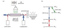
Without complicated processes, in direct demodulation, it is simply to detect the variance of probe laser transmission intensity using photodetector while the Rydberg atom system is at the zero-detune. The photo-generated current is approximately the baseband signal. However, due to the nonlinear relationship between the transmissivity of the Rydberg atom cell and microwave E-field strength, the direct demodulation method will result in nonlinear distortion. The optimum linear operation point of the Rydberg atom system should be studied to decrease the distortion.As far as we know, until now, there is no theoretical analysis about the optimal linear operation point of the Rydberg atom system, and the relationship between the baseband signal amplitude and nonlinear distortion in the AM microwave demodulation. We focus on the optimal linear operation point and nonlinear distortion in the Rydberg atom system.Firstly, we analyze the AM microwave direct demodulation model of the Rydberg atom system. In this model, we explain the nonlinear relationship between probe laser transmissivity and microwave E-field strength.Secondly, we calculate the first and second derivatives of probe laser transmissivity concerning microwave Rabi frequency and analyze the relationship between the first/second derivatives and optimal linear operation point.Thirdly, we adopt total harmonic distortion (THD) to explore the relationship among the Rydberg atom cell operation point, the baseband signal amplitude, and the nonlinear distortion.When THD is introduced to describe the degree of demodulation nonlinear distortion, we find two parameters that will affect the THD value. One is the operation point of the Rydberg atom system, and the other is the Rabi frequency of the microwave baseband signal.The simulation shows that by adjusting the operation point, THD will reach a minimum value, which is consistent with the value that we obtain theoretically from the transmissivity second derivative of zero.Fig. 4(b) shows that when the system is at the optimum linear operation point, the nonlinear distortion of the system declines with the decreasing baseband signal amplitude. Meanwhile, by comparing the THD at three different coupling laser Rabi frequencies, we find that the demodulation nonlinear distortion can be reduced by increasing the coupling laser Rabi frequency.ObjectiveRydberg atom system can strongly respond to weak microwave signals on the electromagnetically induced transparency (EIT) effect and Aulter-Townes (AT) effect. Therefore, people want to utilize this system to detect and demodulate microwaves instead of the traditional mode. At present, there are two methods to demodulate amplitude modulation (AM) microwave signals using the Rydberg atom system, including indirect demodulation and direct demodulation. In the indirect method, the first step is to scan the probe or coupling laser frequency near the zero-detune point, and the second step is to measure the splitting peak-to-peak frequency separation in the probe transmission spectrum. The third step is to calculate the microwave electric field (E-field) strength because the above frequency separation is proportion to the microwave E-field strength.MethodsWe build a simplified Rydberg atom system model (Fig. 1) and numerically simulate the probe laser transmissivity in the Rydberg atom system when 133Cs (energy levels of 6S1/2, 6P3/2, 47D5/2, and 48P3/2) is chosen as Rydberg atom. Our simulation assumes the coupling laser Rabi frequencies separately are 2π×2.7 MHz, 2π×3.2 MHz, and 2π×3.7 MHz. Additionally, our simulation is kept under the frequency-zero-detune, which means probe and coupling laser frequencies are both locked to the energy transition frequency of the Rydberg atom. In these conditions, we conduct the following research.Results and DiscussionsBy mathematical analysis we obtain the optimal linear operation point of the Rydberg atom system from the second derivative of zero (Fig. 3). When the system is operating at that point, the nonlinear distortion of AM microwave demodulation is minimum.ConclusionsWe study the relationship between the nonlinear distortion and the operation point in the Rydberg atom system demodulating the AM microwave signals by the direct method. First, we analyze the demodulation model of the Rydberg atom system in the frequency-zero-detune condition. Second, we calculate the first and second derivatives of the probe laser transmissivity for the microwave Rabi frequency. Utilizing the second derivatives of zero, we find the optimal linear operation point of the Rydberg atom cell in which the nonlinear distortion is the minimum in demodulating AM microwave. Third, the THD is adopted to explore the relationship between the operation point of the Rydberg atom cell, the baseband signal amplitude, and the nonlinear distortion. The simulation shows that the THD of the demodulation system with the Rydberg atom 133Cs (energy levels of 6S1/2, 6P3/2, 47D5/2, and 48P3/2) can reach -95.4984 dB, when the Rydberg atom cell is near the optimum operation point, at 2π×2.7 MHz (coupling laser Rabi frequency) and 1 mV/m (baseband signal electrical field amplitude).
ObjectiveAiming at insufficient research on polarization characteristics of infrared multi-coated targets, we propose a transmission model of infrared polarization characteristics of multi-coated targets. In the modeling of infrared polarization characteristics, most researchers focus on target surface roughness, ambient temperature, different target materials, and different kinds of coatings, but the comprehensive effect of these influencing factors and the multi-coated targets are seriously insufficient. In real life, the protection and camouflage effect of single-layer coatings on the targets is far worse than that of multi-layer coatings. Multi-layer coatings help homogenize the target during brushing, making the target surface smoother. Meanwhile, multi-layer coatings can independently design the coating type and thickness according to the coating effect of the target, which greatly expands the application range and functionality of the target coating. Therefore, we hope to propose a multi-coated infrared polarization transmission model. Based on this model, we can simulate the infrared polarization characteristics of multi-coated targets by simulating multi-coated targets. Then, the infrared radiation polarization characteristics of different materials under different coatings and coating quantities can be studied. This is of significance for the research on new infrared polarization stealth materials and infrared polarization of multi-coated targets.MethodsThe infrared polarization transmission model of multi-layer coatings has two main theoretical bases. First, for the infrared radiation model of the target, we divide the infrared radiation received by the detector into the intensity of the target spontaneous radiation and the intensity of the infrared radiation reflected by the target surface. The infrared radiation intensity of the target's spontaneous radiation is related to the target's emissivity. The higher target emissivity leads to higher spontaneous radiation intensity of the target. Similarly, the lower emissivity brings higher radiation intensity of the spontaneous radiation. This is why a large number of researchers try to reduce the spontaneous radiation intensity of the target by decreasing the target emissivity to achieve low target detectability as far as possible and then the infrared stealth effect. In infrared polarization, reducing the target emissivity is also a common method. Similarly, the ambient thermal radiation ratio has a strong influence on the infrared polarization characteristics of the target. By employing the control variable method, we study the target infrared linear polarization degree under the same ambient heat radiation ratio, different observation angles, and different coating layers. It is compared whether there are coatings to study the infrared linear polarization degree of spontaneous radiation of the target at different observation angles. In addition to the simulation, we adopt infrared linear polarization imaging to study the infrared polarization degree of the target in actual observation conditions.Results and DiscussionsFirstly, we analyze and derive the infrared radiation polarization model of the target according to the existing research on infrared polarization characteristics. Then, according to the geometric model hypothesis, the infrared polarization characteristics of the target under the multi-layer coatings are modeled, and the infrared polarization transmission model of the target under the multi-layer coating is built. By utilizing modern computer simulation technology, the infrared polarization characteristics of the target are simulated by controlling the influence factors such as the layer number in the model and the environmental heat radiation ratio. After the simulation, we verify the coatings with different layers through the experiment of design control variables. The simulation and experiment show that under the same coating quantity, the infrared linear polarization degree of the target increases first and then decreases with the rising observation angle. At the same observation angle, the infrared linear polarization degree of the target gradually decreases with the increasing layer number. This proves that under the experimental target and the coating, the layer number has a significant inhibition effect on the infrared linear polarization degree of the target, and with the increase in the layer number, the peak value of the linear polarization degree gradually moves to the smaller observation angle.ConclusionsWe analyze and calculate the reflected radiation, spontaneous radiation, and the interaction between reflection and spontaneous radiation of multi-coated targets. According to the analysis model of infrared polarization characteristics of target in a thermal radiation environment, the infrared polarization characteristics of multi-coated targets are studied. The results show that the coating number affects the polarization characteristics of both reflected radiation and spontaneous radiation, and the influence degree varies with the coating number. Then, we study the infrared polarization characteristics of multi-coated targets in a thermal radiation environment and discuss the effects of coating quantity and environmental thermal radiation ratio on infrared polarization characteristics. The experimental environment is set up to verify the simulation results, and the results show that the measured data has a good fit with the simulation data. Finally, the theoretical basis and influence of deviation between measured data and simulation data are analyzed. The experimental results show that the model is well fitted and the simulation model has good precision.
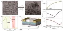
The photovoltaic photodetector structure is Al2O3/ITO/HgTe/Ag2Te/Au. Fig. 2(a) shows the structure diagram and cross-sectional SEM of high-mobility photovoltaic photodetectors. In ambient conditions, a layer of about 50 nm ITO electrode is deposited on the Al2O3 substrate. The ITO serves as electron contact, and then a layer of HgTe CQDs film with high carrier mobility obtained by mixed ligand exchange is deposited by drop-coating. The CQDs film is an intrinsic type regulated by surface doping, which helps increase photocurrent. The HgTe CQDs surface is treated with EDT, HCl, and IPA (1∶1∶20 by volume), with the CQDs thickness of around 400 nm. The Ag2Te nanoparticle solution (Ag+ as P-doping) is prepared on the HgTe CQDs film by spin-coating. It is then exposed to 10 mmol/L HgCl2/methanol solution, which is helpful to diffuse Ag+ into the CQDs film. Finally, a layer of gold electrode is evaporated on top with 50 nm thickness. The energy diagram is shown in Fig. 2(b).ObjectiveShort-wave infrared (SWIR) and mid-wave infrared (MWIR) bands catch much attention because of matching the atmosphere window. In this spectral range, solution-based zinc-blend HgTe colloidal quantum dots (CQDs) become a potential alternative to traditional epitaxial materials for photodetection. However, the performance of CQD photodetectors should be improved, and controlling the transport properties like doping and mobility would be the key to high-performance photodetectors. We employ the mixed phase ligand exchange method to achieve high carrier mobility in HgTe CQDs films, which is more than 1 cm2/(V·s). Meanwhile, different doping types in HgTe CQD solid are realized, such as N, intrinsic, and P types. We also demonstrate that the high carrier mobility improves CQD photovoltaic performance. For example, SWIR and MWIR photovoltaic photodetectors are achieved with intrinsic high mobility HgTe CQDs solid, where the external quantum efficiency (EQE) is 61% for SWIR photovoltaic photodetectors and 30% for MWIR photovoltaic photodetectors. Additionally, the detectivity (D*) is 4×10¹¹ Jones at 300 K for SWIR photovoltaic photodetectors and 1.2×10¹¹ Jones at 110 K for MWIR photovoltaic photodetectors.MethodsThe mixed-phase ligand exchange process involves liquid-phase ligand exchange and solid-phase ligand exchange. In the liquid phase ligand exchange, 4 mL HgTe CQDs in n-hexane would mix with 160 μL β-ME and 8 mg DDAB in DMF, which is stewed for 10 s to accelerate separation. Then the solution is centrifuged, and after decanting the supernatant, 60 μL DMF is adopted to dissolve the CQD solids in centrifuge tubes to obtain stable CQD ink. In this method, β-ME replaces the long-chain ligand on the CQD surface in the liquid phase, and DDAB is a catalyst to assist CQDs transfer from n-hexane to the polar solvent DMF. The CQD films are prepared by spin or drop coating, and then solid-state ligand exchange with EDT/HCl/IPA (1∶1∶50 by volume) solution is performed for 10 s, rinsed with IPA, and dried with N2. Solid-phase ligand exchange can both remove the additional hybrid ligands on the film surface and stabilize the Fermi level of CQD films. For controllable CQDs doping, as Hg2+ can stabilize electrons in CQDs by surface dipoles, we choose mercury salts such as HgCl2 to regulate CQDs to intrinsic or N types, and in liquid phase ligand exchange, 10 mg HgCl2 is added to obtain intrinsic CQDs, and 20 mg HgCl2 is added to obtain N-type CQDs.Results and DiscussionsMixed-phase ligand exchange includes liquid-phase and solid-state ligand exchange, which can improve carrier mobility and control the doping density of HgTe CQDs by surface dipole regulation. The TEM image of the MWIR CQDs before and after the liquid phase ligand exchange is shown in Fig. 1(a). The spacing between CQDs is reduced with tight arrangement, which can improve the light absorption by HgTe CQDs and is conducive to improving device performance. Field effect transistor (FET) is adopted to measure the mobility and doping level of carriers in the film, and the structure is shown in Fig. 1(c). The FET transfer curves of N-type, intrinsic, and P-type MWIR HgTe CQDs are shown in Fig. 1(d). The slope of the FET transfer curve is utilized to calculate the carrier mobility. The carrier mobility of N-type, intrinsic type, and P-type SWIR and MWIR HgTe CQDs all exceeds 1 cm2/(V·s). The I-V characteristic curves of high carrier mobility photovoltaic photodetectors on SWIR and MWIR are shown in Figs. 3(a) and (b), and the open circuit voltages on SWIR and MWIR photodetectors are 140 mV and 80 mV, which indicates a strong internal electric field. At zero bias, the photocurrents on high mobility SWIR and MWIR devices are 0.27 μA and 5.5 μA respectively. The input optical signal power of SWIR and MWIR at the blackbody temperature of 874 K is 0.29 μW and 5.46 μW respectively, and the responsivity (ℜ) is obtained. At zero bias, ℜ reaches 0.9 A/W (at 300 K) and 1.0 A/W (at 80 K) for SWIR and MWIR devices respectively. The D* of high carrier mobility SWIR photovoltaic photodetectors is 4×10¹¹ Jones in all temperature ranges, and that of MWIR photovoltaic photodetectors is 1.2×10¹¹ Jones at 110 K. Additionally, the EQE increases several-fold in high mobility photovoltaic photodetectors, where it is 61% for SWIR devices and 30% for MWIR devices.ConclusionsThe carrier mobility in HgTe CQD films is increased to 1 cm2/(V·s) by the mixed phase ligand exchange method. By adding salt, the doping control of P-type, intrinsic type, and N-type CQD films is realized. Meanwhile, photovoltaic photodetectors in SWIR and MWIR are prepared based on intrinsic high mobility CQD solid. For the 1.9 μm SWIR photodetectors, ℜ is 0.9 A/W and D* is 4×10¹¹ Jones at 300 K. For the 4.2 μm MWIR photodetectors, ℜ is 1.1 A/W and D* is 1.2×10¹¹ Jones at 110 K. In addition, the EQE would be improved to 61% for SWIR photodetectors at 300 K and 30% for MWIR at 110 K, without applied bias. The test results show that the transport property control of CQDs can improve the core performance of photodetectors, such as ℜ and D*. Our study can promote the development of low-cost and high-performance CQDs infrared photodetectors.
ObjectiveThe fiber Fabry-Perot (F-P) filter plays a critical role in fiber Bragg grating (FBG) wavelength demodulation systems. However, the continuous drift in the transmission wavelength and driving voltage curve of the F-P filter due to changes in the ambient temperature can significantly decrease the wavelength demodulation accuracy. To correct the drift error, researchers have proposed several wavelength correction methods, such as the F-P etalon, FBG reference grating, and gas absorption line reference methods. Despite high accuracy, these methods can increase the system's cost and complexity. Recently, with the increased applications of artificial intelligence, machine learning methods have emerged as a novel and highly portable option for correcting temperature drift errors in F-P filter at a relatively low cost. Currently, the most commonly employed technique for temperature drift correction is support vector machine (SVM), which does not take into account the high temporal correlation among samples before and after temperature drift data. To this end, we propose an Attention-LSTM network-based temperature drift correction method for F-P filters. The temperature drift data for the F-P filter is a typical time series with dynamic characteristics, indicating that the current drift depends both on the present input and the past input. We adopt the LSTM model for feature extraction and apply the attention mechanism to assign different weights to various input features. The combination of short-term and long-term memory, along with the attention mechanism, enhances the demodulation accuracy of the F-P filter.MethodsWe select FBG0 as the reference grating and the other three FBGs as sensing gratings. The input features employed in the model include temperature, temperature change rate, and the spectral position of FBG0. The output of the model is the absolute wavelength drift of sensing FBG3. Due to the strong temporal correlation in the temperature drift data of the F-P filter, a fixed length of time series samples is first selected, and then a multi-temporal training dataset is obtained by sliding it successively in a backward direction. By adopting the LSTM algorithm, the hidden states are generated for each time step by learning the input information of the current and past times and are then integrated into a context vector that serves as the input for the attention layer. The attention layer processes the data further by assigning weights to give significant information larger values, highlights important information, and filters out useless information, thus improving the model's prediction accuracy. The ReLU layer is employed after the attention layer to enhance the model's non-linear fitting abilities. Finally, a linear layer is adopted for dimensionality reduction to obtain the temperature drift prediction results of the F-P filter. The proposed model's effectiveness is validated by comparing it to the traditional LSTM model in the same temperature environment.Results and DiscussionsIn a heating-cooling-heating temperature variation environment, the proposed model is compared to a traditional LSTM model in error correction results of temperature drift for the three sensing gratings (Table 2). Experimental results show that the maximum temperature drift correction error of the traditional LSTM model is 16.64 pm, while the Attention-LSTM model reduces the maximum temperature drift correction error to 6.75 pm. Additionally, the proposed model is compared to common temperature drift models such as LSSVM, RNN, and LSTM in a slowly changing monotonous cooling environment (Table 3). Experimental results indicate that the performance of the Attention-LSTM model is superior to other temperature drift models. The above experimental results demonstrate that the proposed model integrates the attention mechanism with traditional LSTM models for time series modeling. This model adopts LSTM to extract long-term and short-term data sample information over time and the attention mechanism to assign different weights to the sample features. As a result, important feature information is highlighted, and the demodulation accuracy and stability are improved.ConclusionsWe thoroughly consider the time correlation between temperature drift data samples and the dynamic drift law. We not only take into account the influence of current inputs on the drift amount but also capture the effect of past inputs on the demodulation results. The LSTM model is employed for feature extraction and an attention mechanism is introduced to propose an F-P filter temperature drift error correction method based on the Attention-LSTM network. The attention mechanism assigns different weights to different features in the model to improve the modeling accuracy of the LSTM model. We conduct temperature drift error correction experiments in two temperature variation environments and compare the Attention-LSTM model with traditional LSTM model, RNN model, and LSSVM model. Experimental results demonstrate that the performance of the Attention-LSTM model in temperature drift error correction is significantly better than that of other models, with a MAXE of only 5.39 pm and MAE and RMSE of just 2.07 pm and 2.62 pm respectively. Meanwhile, compared to traditional hardware methods, the proposed error correction method based on the attention mechanism and LSTM network is low-cost with high portability, as it does not require any hardware equipment. This approach provides a new perspective for temperature drift error correction of tunable F-P filters.
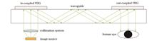
ObjectiveThe performance of a volume holographic grating as an incoupling/outcoupling element seriously affects the field of view (FOV) of a waveguide system. Many studies try to extend the incident angle response bandwidth of the volume holographic gratings to increase FOV. Most volume holographic gratings are designed based on the center ray. However, in a waveguide system, the collimation system converts the position information on the image source into angular information, which makes the beam incident to the volume holographic grating within a certain angle range (Δθ). Based on the Kogelnik theory, the angular range of the diffracted beam Δθ' is much larger than Δθ. Since the diffracted beam of the incoupling grating is the incident beam of the outcoupling grating, the mismatch between Δθ and Δθ' will make the outcoupling grating cannot fully receive all the angular information in the diffracted beam, causing insufficient transmitted image information. We propose a design method of multiplexed volume holographic gratings. The response bandwidth of the outcoupling grating is increased through multi-time multiplexing, while the diffraction angle offset range of the incoupling grating is reduced to match its bandwidth as much as possible, which can guarantee that enough image information can be received to increase the FOV of a waveguide system.MethodsThe analysis reveals that the factors limiting the FOV of the waveguide system include not only the response bandwidth of the volume holographic grating itself but also the bandwidth mismatch between incoupling grating and outcoupling grating. Therefore, a design method of multiplexed volume holographic gratings is proposed. The object and reference light preparation angles of a single grating are determined according to the total reflection condition of the waveguide. The diffraction efficiency corresponding to each of its angles is calculated, as well as the response bandwidth of the incoupling grating, the diffracted light angle of the incoupling grating, and the response bandwidth of the outcoupling grating. The diffracted light angle range of the incoupling grating is revealed to be much larger than the response bandwidth of the outcoupling grating, with a bandwidth mismatch. According to the multiplexed coupled wave theory, the bandwidth extension of the multiplexed gratings can be compounded together in a similar way as superposition. Based on the angular range of the bandwidth mismatch occurrence, the response bandwidth of the outcoupling grating is expanded by the multiplexed method, and the diffracted light angle of the incoupling grating is contracted at the same time. This makes the incoupling/outcoupling grating bandwidths match as much as possible, compensating for the lack of some image information when the waveguide system is imaged.Results and DiscussionsFirstly, the diffraction efficiency corresponding to each of its angles is calculated based on the parameters of the designed single grating (Fig. 3). Meanwhile, image simulation is performed by simulation software (Fig. 6) and the diagonal FOV of the waveguide system is 16.1°. The horizontal FOV is too small, resulting in the inability to fully couple out the image coupled into the waveguide. Therefore, the multiplexed grating angle is designed (Fig. 4) to match the incoupling/outcoupling grating response bandwidths. The FOV is further extended to 18.7° (Fig. 7). The angular information of the coupled-in waveguide should be increased to further increase the FOV. Triple multiplexing is performed based on the secondary multiplexing, and the response bandwidth of the incoupling grating is extended simultaneously (Fig. 8). The simulation results show that the diagonal FOV can reach 22.9° (Fig. 9). The multiplexed volume holographic grating designed by this method is simple to prepare and can expand the FOV of the waveguide system.ConclusionsWe first analyze the bandwidth mismatch in the incoupling/outcoupling gratings of the waveguide system. The factors limiting the FOV of the holographic waveguide system are not only the response bandwidth of the volume holographic grating itself but also the bandwidth mismatch between the incoupling grating and outcoupling grating. Therefore, a design method of multiplexed volume holographic grating is proposed to control its diffraction angle and the response bandwidth of the outcoupling grating. Based on the multiplexed coupled wave theory, the secondary multiplexed grating is first designed. Additionally, the response bandwidth of the outcoupling grating is expanded and the contraction of its diffraction angle is realized at the same time. The image simulation and the optimized design of triple multiplexing are further carried out, whose diagonal FOV of the holographic waveguide system is improved to 22.9°. The FOV of the waveguide system can be further enlarged by more times of multiplexed design. The designed multiplexed holographic grating is simple to prepare and can extend the FOV of the waveguide system with limited refractive index modulation.
ObjectiveThe concentration of greenhouse gases in the earth's atmosphere is increasing year by year under the influence of fuel burning, deforestation, and industrial development. The continuous emission of greenhouse gases will result in increased global temperature and extreme weather such as heavy rainfall and sea level rise. Remote sensing of greenhouse gases is an important method for tracking greenhouse gas emissions and understanding the earth's climate evolution. As one of the most important optical payloads for spaceborne greenhouse gas monitoring, the grating imaging spectrometer features high resolution, high signal-to-noise ratio, and nearly linear dispersion. The immersed grating can achieve higher spectral resolution and more compact structural size and has been employed as the dispersion elements in imaging spectrometer for remote sensing of greenhouse gases. Currently, immersed gratings with higher performance are required to fulfill the requirements for more accurate greenhouse gas monitoring. For conventional reflective immersed gratings, metallic coatings are adopted to reflect the incident light. However, there are many disadvantages for the metallic coating. Firstly, this coating may cause resonance absorption due to the plasmon effect. The resonance absorption will decrease the diffraction efficiency and increase the polarization sensitivity of the grating. Secondly, it is difficult to deposit metal materials on the grating groove, which will also cause decreased diffraction efficiency. To this end, we propose and design a total internal reflection immersed grating whose grating groove is coated with nano laminate. It has high diffraction efficiency and low polarization sensitivity and can be utilized in the O2-A channel for the imaging spectrometer of greenhouse gas monitoring.MethodsAccording to the monitoring requirements of greenhouse gases, the design of the immersed grating is as follows. Firstly, the grating structure is modeled by the finite element software, and the diffraction efficiency and polarization sensitivity of the initial structure are calculated. Then, the parameters such as the duty cycle of the grating, the thickness of the nano laminate, the groove depth, and the refractive index of the nano laminate are optimized in turn with the controlled variable method. According to the optical film theory and the actual coating method, the thickness and stacking sequence of the nano laminate are optimized, and the multi-layer film structure is obtained. Finally, the manufacturing tolerance of the designed immersed grating is analyzed, and the tolerance of the grating with diffraction efficiency greater than 90% and polarization sensitivity less than 1% is presented.Results and DiscussionsBased on the introduced design method, an immersed grating working under the total internal reflection and coated with the nano laminate is designed, and it has high diffraction efficiency and low polarization sensitivity. Benefiting from the advantages of total internal reflection, the designed immersed grating has no transmission order, and the diffraction light energy is concentrated on the reflection diffraction order, which is helpful to improve the diffraction efficiency. Additionally, the coating on the grating groove is the nano laminate structure, which is alternately stacked with Al2O3 and TiO2 materials (Fig. 7). The nano laminate can improve the diffraction efficiency of the grating in the transverse electricity (TE) and transverse magnetism (TM) directions, and reduce the polarization sensitivity. The results show that the average diffraction efficiency of the design immersed grating at the -1 order is higher than 92%, and the polarization sensitivity is lower than 1% in the working band of 750–770 nm (Fig. 8).ConclusionsOur paper provides the spectral resolution formula of immersed gratings based on the principle of immersed gratings and shows that the immersed grating can reduce the size of the optical system and achieve high spectral resolution. According to the working conditions and grating parameters given by the optical design, fused silica is selected as the grating substrate, and a total internal reflection immersed diffraction grating with high diffraction efficiency and low polarization sensitivity is designed. The corresponding manufacturing tolerances are analyzed by considering the diffraction efficiency and polarization sensitivity requirements and the manufacturing method. The presented reflective immersed grating in our paper has the advantages of high diffraction efficiency and low polarization, and the grating groove tolerance is feasible for manufacturing. Therefore, our study lays a basis for the design of high-performance reflective immersed gratings.
ObjectiveWhite light interferometry, as an effective non-destructive method, is widely employed for measuring characteristic parameters of microstructures. Among these microstructures, the rectangular grating is a typical periodic step structure and has extensive utilization in precision machining due to its diverse materialization properties based on surface morphology characteristic parameters. However, when the groove depth of the grating is smaller than the coherence length of the adopted light source, the batwing effect occurs near or at the edge of the step in the sample under measurement. ISO series 25178 provides a standard morphology for calculating the characteristic parameters of groove depth and linewidth through three-dimensional surface morphology analysis, which necessitates determining the position of the step edge. The batwing effect poses challenges to precisely locating the step edge position and may result in a false representation of information near the edge of the step discontinuity. We propose a new algorithm for determining the characteristic parameters of rectangular gratings by utilizing the distribution difference of the coherence signals between the upper and lower surfaces, thus avoiding the traditional method of extracting step edge position from three-dimensional surface morphology. The introduced algorithm demonstrates excellent measurement accuracy, high repeatability, and exceptional robustness in calculating the desired characteristic parameters of rectangular gratings.MethodsWe propose an algorithm for precise positioning of the step edge in rectangular gratings based on the distribution difference of the coherence peak among different sampling points. The algorithm is designed to improve the detection efficiency of characteristic parameters by incorporating parallel processing techniques. Firstly, during vertical scanning, the coherence signals undergo modulation. Simultaneously, the contrast information is obtained by the gravity method to extract the center of gravity position of the modulation envelope across all sampling points within the field of view. Then, the peak of the contrast envelope is calculated to further accentuate the discrepancy between the upper and lower surfaces of the rectangular grating. By identifying these surfaces, we acquire the step position information, which allows to generate the mask matrix and determine the linewidth values. To obtain the groove depth, we combine the mask matrix and three-dimensional surface morphology of the rectangular grating. Meanwhile, we extend the application of the "W/3" guideline specifically for the rectangular grating structure to mitigate the influence of the batwing effect on depth measurements. Additionally, we incorporate the Stoilov algorithm to calculate the contrast information during the vertical scanning, enabling simultaneous determination of the step edge position and three-dimensional surface morphology. This parallel processing approach enhances the efficiency and accuracy of the algorithm. Generally, our algorithm provides an effective means for precisely positioning the step edge in rectangular gratings, while considering the influence of the batwing effect on depth measurements.Results and DiscussionsExperiments are conducted via a self-developed white light interferometry system to evaluate the feasibility and accuracy of the proposed method. Two rectangular gratings with different characteristic parameters are selected as measurement samples. The first sample calibrated by Physikalisch-Technische Bundesanstalt (PTB) has a groove depth of 189.6 nm±1.0 nm and a linewidth of 6 μm. The second sample certified by VLSI standards traceable to the National Institute of Standards and Technology (NIST) has a groove depth of 90.5 nm±2.8 nm and a linewidth of 50 μm. Ten repeatability measurements are performed in the same area of each sample based on the proposed algorithm. For the first sample, the average depth value is determined to be 188.97 nm with a relative error of 0.33% [Fig. 8(a)]. The average linewidth value is measured to be 6.12 μm with a relative error of 2% [Fig. 8(b)]. Similarly, for the second sample, the average depth value is 90.10 nm with a relative error of 0.40% [Fig. 8(c)]. The average linewidth value is determined to be 99.04 μm with a relative error of 0.96% [Fig. 8(d)]. These measurement results demonstrate the accuracy and effectiveness of the algorithm. Furthermore, the standard deviation of the ten repeatability measurement results is analyzed to assess the algorithm stability. The small standard deviation confirms the consistent and reliable performance of the proposed method. Additionally, the influence of error terms during the experiment on the measurement results is investigated. Specifically, variations in sample placement tilt angle, interference fringe numbers, and interference fringe direction are examined. The results indicate that these error terms exert minimal effect on the measurements, highlighting the robustness of the proposed algorithm. In general, the experimental results validate the feasibility and accuracy of the algorithm in accurately determining the groove depth and linewidth of rectangular gratings. The algorithm exhibits stability and robustness and becomes a reliable tool for precise metrology in surface morphology measurements.ConclusionsWe present a new approach for accurately measuring the characteristic parameters of rectangular gratings under the batwing effect. Unlike conventional calibration methods, our method focuses on the distribution difference of coherence signals between the upper and lower surfaces of the grating. This approach addresses the limitations of ISO series 25178 in accurately measuring the characteristic parameters in the presence of the batwing effect. To validate this method, we conduct simulations of interferograms during the vertical scanning based on linear system theory. By analyzing the modulation envelope of these interferograms, we can precisely detect the step edge position and distinguish the upper and lower surfaces of the grating sample. Finally, by applying ISO standards, we accurately measure the characteristic parameters of the rectangular grating. Experimental results using two rectangular gratings with different groove depths and linewidths demonstrate the repeatability and robustness of our method. The implementation of the "W/3" guideline in measuring rectangular gratings is significantly improved to accurately measure the characteristic parameters. Importantly, our method features high efficiency, high precision, and fine repeatability without requiring any physical upgrades to the instrument. Considering the ongoing trend towards miniaturization of rectangular gratings, our method has broader applications.
ObjectiveMicrowave frequency measurement technology plays an important role in various defense and civil applications, such as electronic warfare, radar, and wireless communications. Microwave frequency measurements can be achieved by conventional electrical methods. Although high-resolution multi-frequency signal measurement is achieved, the frequency measurement range is limited by electronic bottlenecks, and the measurement system is susceptible to electromagnetic interference, while photonic-assisted frequency measurement based on photonics can not only overcome such problems but also has the advantages of high flexibility and high speed. In general, photonic-assisted instantaneous frequency measurement systems work in three ways, which are frequency power mapping (FTPM), frequency time mapping (FTTM), and frequency space mapping (FTSM). FTPM-based schemes have the advantages of good real-time performance and high accuracy, but most of them have great difficulties in measuring multi-frequency microwave signals. FTTM-based schemes are easy to implement the measurement of multi-frequency signals, but they are not applicable in scenarios with real-time requirements. FTSM-based schemes are suitable for handling multi-frequency signals while obtaining accurate frequency information in real time, but they often require filter arrays or wavelength division multiplexers (WDM), which can increase the system complexity and reduce the flexibility of the system. To address the problems of the FTSM-based scheme, we propose a multi-frequency signal transient detection scheme without optical filtering.MethodsThe experimental system is built by using optical simulation software. The system uses a non-flat optical frequency comb modulated by a sawtooth wave to determine the frequency range of the signal by using the beat-to-beam power ratio of the signal to be measured and the optical frequency comb as a reference and then calculates the exact frequency of the signal to be measured from the demodulated frequency information. The system uses the multi-frequency signal to be measured and the sawtooth wave to be modulated together, and the generation of non-flat optical frequency combs is realized while loading the electrical signal. The frequency information can be processed by a computer such as fast Fourier transform, and the multi-frequency measurement system can be realized in this way. In this paper, an electrical spectrum analyzer (ESA) is used to obtain the beat frequency results.Results and DiscussionsFirstly, the system is verified with single-frequency signal and multi-frequency signal, and the results are shown in Fig. 4 and Fig. 5, respectively, which are in accordance with the theoretical results. Then the frequency measurement is carried out within the measurement range of the system in steps of 300 MHz, and the measurement results are shown in Fig. 6, with the absolute error within 40 MHz, but two of the sampling points could not be measured because the signal frequency to be measured is in the middle and border position of the channel, resulting in the inability to get paired electrical signals after tapping the frequency. For such problems, another branch with different channel width is added to the original system. In addition, as the system is susceptible to noise, it is easy to cause the power ratio of weak signals to be unstable, so the influence of the power of the signal to be measured on the measurement results is analyzed, as shown in Fig. 9. The power ratio of the signal to be measured starts to stabilize from -10 dBm. Due to the internal waveguide structure and material of Mach-Zehnder modulator (MZM), the static operating point of its direct current (DC) bias voltage will shift with the change of external factors such as temperature, which will greatly affect its operating characteristics and system performance, so the bias voltage drift of MZM is discussed. It can still be measured accurately within the floating range of 1% up and down, and the results are shown in Fig. 12.ConclusionsIn summary, a channelized multi-frequency measurement system based on a non-flat optical frequency comb is proposed and analyzed. The sawtooth wave spectral power decreases step by step, and it is modulated into the optical domain by suppressing the carrier bilateral band modulation, which can form the non-flat optical frequency comb required by the system. When the signal is measured, the signal to be measured will be co-modulated with the sawtooth wave. This way can avoid the unbalanced change of multi-branch detection while reducing the complexity of the system and improving the stability of the system. By changing the sawtooth wave frequency, the measurement range of the system can be adjusted, which has a certain degree of flexibility. The simulation achieves multi-frequency measurements in the range of 0.3-40 GHz with an error of less than 40 MHz and a relative error of better than 4%. In addition, the power variation of the radio frequency signal to be measured and the effect of MZM bias voltage drift are analyzed, and the results show that the power ratio of the signal to be measured starts to stabilize from –10 dBm, and the frequency judgment is accurate. The system has a certain tolerance to the MZM bias voltage drift, and it can still measure accurately within ±1% variation.
ObjectiveAs an interdisciplinary topic, microwave photonics has important applications in fields of broadband optical wireless communications, radars, and electronic warfare, due to the intrinsic characteristics of large bandwidth, high resolution, tunability, reconfiguration, and immunity to electromagnetic interference. In recent years, demodulation techniques based on microwave photonics have attracted considerable research interest, through the sensing information conversion from the optical domain to the microwave domain and high-resolution electrical spectrum analysis and processing techniques. When microwave photonic demodulation technology is applied to multi-point or quasi-distributed fiber Bragg grating (FBG) sensing systems, the RF response curve of the sensing system is usually transformed from the RF domain to the time-domain by discrete inverse Fourier transform (IDFT). Meanwhile, the sensor demodulation is realized by analyzing the amplitude of the peak point of impulse response in the time domain or the position change on the time axis. When traditional microwave photonic demodulation technology based on frequency-time transformation is applied to the FBG sensor network, it is necessary to ensure that no superposition is generated in the corresponding time-domain response signal for guaranteeing accurate demodulation of each FBG. This puts forward strict requirements for the spatial interval and wavelength separation between FBGs and limits the application range of microwave photonic demodulation technology. To this end, an effective meta-heuristic algorithm, arithmetic optimization algorithm (AOA) is introduced into the microwave photonic demodulation technology based on frequency-time transformation to realize precise demodulation of multiple FBG peaks under the time-domain signal superposition.MethodsAOA is a newly developed meta-heuristic search technique that simulates the distribution characteristics of the basic arithmetic operations of addition, subtraction, multiplication, and division and has been employed to solve some real-world optimization problems. It is mainly divided into three stages including initialization, exploration, and development. During the exploration stage, Math optimizer accelerated functions are adopted to select different search strategies. At the beginning of this stage, AOA takes advantage of the characteristic that the multiplication and division operators are widely distributed and are difficult to approach the target to complete the global optimization in the search space and thus jump out of the local optimum. At the end of the exploration stage, AOA leverages the characteristic that the addition and subtraction operators are lowly distributed and easy to approach the target to achieve local optimization in the search space and further improve demodulation accuracy in a more accurate search space.Results and DiscussionsIn a proof-of-concept experiment, a sensor network consisting of six FBGs with different wavelengths is built. The scanning range of vector network analyzer (VNA) is set to 10 MHz-5 GHz, the sampling resolution is 5 MHz, and a total of 1000 sampling points are included. In the experiment, the two ends of the sensing FBG are fixed on the two 3-axis translation stages via AB glue, with the distance between the two fixed points being 10 cm. The strain applied on the sensing FBG can be adjusted by moving one of the two translation stages, and it is linearly increased from 0 με to 2000 με with a step size of 100 με. It should be pointed out that by changing the strain applied to the sensing FBG, the time-domain sinc peaks corresponding to two FBGs will experience three conditions of non-overlapping, partially overlapping, and completely overlapping. The experiment results show that AOA can determine the central wavelength of each FBG regardless of the overlapping situation of the time-domain pulse signal, indicating that this method is suitable for the demodulation of time-domain overlapping signals (Fig. 8). To further validate AOA's demodulation performance, we conduct a comparison between AOA and other six meta-heuristic methods. The results confirm that, compared with other meta-heuristic algorithms, AOA has better performance in convergence efficiency, demodulation speed, and demodulation precision. Additionally, AOA solves the defect that the traditional meta-heuristic algorithm is prone to fall into the local optimal solution (Fig. 9 and Table 4).ConclusionsWhen traditional microwave photonic technology based on frequency-time transformation is employed in the demodulation of FBG sensor arrays, it is necessary to ensure that the pulse signals of the time-domain response curve do not overlap, otherwise, huge demodulation errors will be caused to severely limit the application range of microwave photonic demodulation technology. To solve this problem, we introduce a time-domain overlapping signal peak detection method based on an arithmetic optimization algorithm. The proposed method transforms the demodulation of time-domain overlapping signals into multi-parameter optimization and achieves precise demodulation of time-domain peaks under signal overlapping through mathematical modeling. Comparison with the other six meta-heuristic algorithms shows that AOA exhibits sound performance in convergence efficiency, demodulation speed, and demodulation accuracy. Meanwhile, it solves the defect that traditional meta-heuristic algorithms are prone to fall into local optima to improve the demodulation of microwave photonic demodulation technology for dense FBG sensing networks.
ObjectiveResearch on hybrid dual-hop radio frequency (RF)/free-space optical communication systems can improve the multipath fading robustness and communication coverage. However, since the co-channel interference problem in RF communication systems cannot be ignored, the adoption of a multi-user diversity scheme can improve the adverse interference effect and enhance the system performance. Meanwhile, optical reconfigurable intelligent surface (RIS) is introduced in the free-space optical (FSO) communication link to enhance the signal quality when the FSO communication cannot fulfill the conditions of line-of-sight communication.MethodsTo improve the co-channel interference in RF communication, we utilize the simultaneous transmission of multiple users to generate diversity gain and consider the problem that FSO communication cannot complete line-of-sight transmission. Additionally, RIS technology is introduced in the FSO link to put forward a scheme of RIS-assisted MUD-RF/FSO hybrid system under co-channel interference. The RF link with multi-user diversity obeys the independent homogeneous Rayleigh distribution, the optical RIS-assisted FSO link obeys the Gamma-Gamma distribution, and the decode-and-forward protocol is adopted at the electro-optical conversion relay node. Based on the probability density function (PDF) of the system's end-to-end instantaneous signal to noise ratio (SNR) and its cumulative distribution function (CDF), closed expressions for the system outage probability and average bit error ratio (BER) are derived. Simulation results show that RIS can significantly improve the performance of the MUD-RF/FSO hybrid system, and the increasing user number can bring diversity gain to the system, thus suppressing the undesirable effects caused by co-channel interference.Results and DiscussionsIn strong turbulence conditions, the SNR of the FSO link is fixed at 50 dB to study the effect of different L and M on the outage probability of the system. The outage probability performance of the system is dramatically improved when the user number is changed from L=1 to L=2. This is attributed to the simultaneous transmission of multiple users generating a diversity gain (Fig. 2). Meanwhile, the SNR of the RF link is fixed to be 50 dB under strong turbulence to study the effect of different numbers of RIS reflection element surfaces and threshold values on the system interruption probability. When the threshold value is decreased from 4 dB to 1 dB with N=8, the system has a gain of about 3 dB under the interruption probability of 10-3, indicating a great effect of different threshold values on the system performance. When the SNR of the FSO link is greater than 50 dB, the system interruption probability remains basically unchanged, which shows that the RF link plays a dominant role at this time. Under the same threshold, with the rising reflective elements on the optical RIS, the interruption probability of the system gradually decreases, which is because the increase in reflective elements can improve the channel quality of the FSO link and enhance the system performance (Fig. 3). The SNR of the RF link and FSO link are both fixed at 30 dB to compare the effect of different aperture radii and beam widths on the system outage probability. As the ratio of the aperture radius and the beam width increases, the system outage probability decreases. The system performance deteriorates when the turbulence intensity changes from weak turbulence intensity to strong turbulence intensity, indicating that the turbulence intensity can exert great influence on the FSO link (Fig. 4). To determine the effect of standard deviations of different pointing error angles and intelligent channel reconfigurable node (ICRN) deflection error angles on the average bit error rate of the system, we set the SNR of a fixed RF link as 20 dB in strong turbulence conditions. The smaller standard deviation of the pointing error angle and ICRN deflection error angle leads to a smaller corresponding value of the average bit error rate of the system, and the larger pointing error coefficient brings better system performance (Fig. 7).ConclusionsWe analyze the performance of the RIS-assisted MUD-RF/FSO hybrid system under co-channel interference. RF links obey Rayleigh distribution, RF links in the presence of CCI also obey Rayleigh distribution, decode-and-forward protocol is employed at relay nodes, and optical RIS-assisted FSO links obey Gamma-Gamma distribution. Meanwhile, the closed formulas for the system outage probability and average BER are derived and analyzed numerically. The simulation results show that the RF links play a dominant role at high SNR. The number of interfering signals and their corresponding SNRs have different degrees of influence on the system performance, while the increase in the user number can attenuate the adverse interference effects on the system. The system performance can be enhanced by increasing the number of RIS reflection units, improving the ratio of the aperture radius to the beamwidth, weakening the turbulence intensity, decreasing the threshold value, and lowering the standard deviation of the pointing error angle and the ICRN deflection error angle. Additionally, the best system performance is obtained by BPSK modulation.
ObjectiveOptical fiber waveguide refractive index (RI) sensors have potential applications in environmental monitoring and biochemical sensing due to their low cost, small size, easy operation and integration, high sensitivity and stability, anti-electromagnetic interference, and corrosion resistance. At present, different optical fiber waveguide RI sensors have been proposed, among which U-shaped optical fiber waveguide has become a research hotspot in optical fiber waveguide sensing because of its compact structure, simple preparation, and high sensitivity. On one hand, the preparation parameters of optical fiber waveguide structures are designed and optimized, and on the other hand, the sensitivity of the sensing unit to the external environment is improved by combining new two-dimensional materials to further improve the sensitivity of U-shaped optical fiber waveguide sensors. However, precious metal materials have high losses and preparation costs, with limited response wavelength of two-dimensional materials. Realizing optical fiber waveguide RI sensors featuring low cost, easy operation, and high stability and sensitivity still poses significant challenges. Thus, we propose and implement an interference enhanced hybrid optical waveguide (IE-HOW). The sensor based on IE-HOW is characterized by high sensitivity, low loss, compact structure, and good stability, and it has broad application prospects in biochemical detection, clinical diagnosis, and other fields.MethodsThe beam propagation method is employed to simulate the energy distribution of the optical field before and after the cascade. To prepare IE-HOW, we first fuse a micro-bottle cavity (MBC) on the surface of single mode fiber (SMF) by arc discharge, and then place the SMF containing MBC on the hydrogen-oxygen flame tapering machine for melting tapering. During the manufacturing, precise control of the discharge frequency and propulsion amount of the fusion welding machine controls the MBC size, and parameters such as hydrogen flow rate, step speed, and stretching length of the hydrogen oxygen flame cone pulling machine are controlled precisely. Finally, the bending diameter is controlled reasonably to bend the tapered hybrid optical waveguide into a U-shaped one, and the length and diameter of the MBC are characterized by an optical microscope. The MBC size and bending diameter are kept unchanged, and the stretching lengths are changed (h=16000 μm, h=18000 μm, and h=20000 μm) to prepare ordinary non-interference enhanced micro-nano U-shaped optical waveguide (UOW) and IE-HOW structures with different cone diameters respectively. Meanwhile, RI sensing tests are performed on ordinary UOW without cascaded structures and IE-HOW with cascaded structures to compare their sensitivity. For RI sensing, the change of external environment RI will alter the phase difference between the core mode and the cladding mode, leading to accordingly changed spectrum wavelength. The broadband light source (BBS, from 1250 to 1650 nm) is connected to the IE-HOW input end, and the output transmission spectrum of the output section is recorded in real time by an optical spectral analyzer (OSA, AQ6370D).Results and DiscussionsSolutions with different RI are prepared by NaCl solution and calibrated with Abbe refractometer, with an RI range of 1.333-1.362. In UOW-based RI sensing measurements, the maximum sensitivities of RI sensor tests with cone diameter d1=12.30 μm, d2=7.44 μm, and d3=4.88 μm are 640.06 nm/RIU (1507.5 nm), 913.25 nm/RIU (1487.10 nm), and 2750.32 nm/RIU (1412.70 nm) respectively, with the linearity R2 >0.9 (Fig. 5). In IE-HOW-based RI sensing measurements, the maximum sensitivities of RI sensor tests with cone diameter d1=12.30 μm, d2=7.44 μm, and d3=4.88 μm are 905.21 nm/RIU (1428.10 nm), 2587.22 nm/RIU (1432.50 nm), and 8813.26 nm/RIU (1406.50 nm) respectively, with the linearity R2> 0.9 (Fig. 6). The smaller cone diameter leads to greater RI sensitivity. When the cone diameter of the micro-nano U-shaped fiber is 4.88 μm, the RI sensitivity of IE-HOW is three times higher than that of UOW (Fig. 7). Temperature and stability tests are carried out on IE-HOW with a cone diameter of 4.88 μm respectively. The sensing unit is placed in a temperature control box, and spectral data are recorded at intervals of 10 °C and stabilized for 10 min within the range of 20-80 °C. The wavelength variation within the range of 60 °C is less than 0.02 nm (Fig. 8). The spectral data are recorded every 10 min at room temperature, and the maximum wavelength change within 1 h is less than 0.02 nm (Fig. 8). Therefore, the high-sensitivity RI sensor based on IE-HOW has high-temperature stability.ConclusionsWe propose and implement a highly sensitive RI sensor based on IE-HOW. By cascading UOW and MBC to construct IE-HOW, interference enhancement and low loss are achieved based on the strong focusing effect of MBC and large bending diameter respectively. Compared to UOW, under the same cone diameter of 4.88 μm, the RI sensitivity is increased by 3 times, reaching 8813.26 nm/RIU, and R2> 0.9. This sensor has advantages such as high sensitivity, low loss, all fiber, low cost, and good stability, with practical significance in biosensing, environmental monitoring, and other fields that require high RI sensitivity.
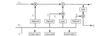
ObjectiveConventional phase generation carrier (PGC) demodulation methods include two main approaches of differential and cross multiplying PGC (PGC-DCM) and arctangent PGC (PGC-ARCTAN). Their correct demodulation requires the carrier phase delay and modulation depth to be maintained at specific values. However, in practice, propagation delays in the optical path, analog-to-digital conversion in the signal acquisition system, and interference caused by the PIN photodetector can introduce phase delays between the carrier signal and the modulated carrier signal. Additionally, the modulation depth C is related to the amplitude of the carrier signal and the parameters of the phase modulator, and it changes with the optical wavelength, temperature, and humidity in the actual operating environment, resulting in random drift and fluctuation of C value. These unstable factors directly affect the operation of the entire demodulation system, causing harmonic distortion of the demodulated signal and even demodulation failure. Therefore, solving the instability problems of C value and phase delay is an important task to improve the stability and accuracy of the demodulation system. Nowadays, many scholars have calculated the modulation depth and phase delay by employing different octave carriers compensation to solve this problem and yielded some results. However, the high-order Bessel function and high octave carriers are prone to introduce high-frequency harmonics in the demodulation results, which causes certain nonlinear distortion. Meanwhile, as different multicarriers and different orders of Bessel functions also affect the demodulation results, it is very important to determine the appropriate carrier multiplicity and Bessel order for accurate demodulation.MethodsConsidering the influence of different octave carriers and different orders of Bessel functions on the demodulation results, we propose a multistage orthogonal signal fusion (MOSF) computation method that synthesizes the triple-octave carriers and the third-order Bessel functions. Firstly, the phase delay of the interference signal is calculated and compensated, then the modulation depth is calculated based on the compensated signal, and finally, the compensated demodulated signal is obtained. The signal-to-noise-and-distortion (SINAD) and total harmonic distortion (THD) of the MOSF algorithm and the traditional algorithm in demodulating signals with different phase delays and modulation depths are verified by simulation and experimental comparisons. The linear errors and nonlinear distortions of the demodulation results are analyzed in detail, and then the phase delay errors of the demodulated signals of the different algorithms are compared and analyzed to characterize the real-time performance of the different algorithms. Finally, the ground noise level and the maximum detection range of the demodulated signals of the MOSF algorithm are experimentally analyzed.Results and DiscussionsWe conduct controlled experiments to study the stability of different algorithms. Under the different modulation depth changes, the demodulation results are shown in Fig. 8(a), and the SINAD value of the MOSF algorithm fluctuates up and down in the range of 8 dB-15 dB with the center value of 13 dB. Fig. 8(b) shows the THD of the demodulated signals, and the THD of demodulated signals of the MOSF algorithm is stabilized at -96 dB with a very small fluctuation. It is very small, and under different phase delay variations, the demodulation results are shown in Fig. 9(a). The SINAD value of the MOSF algorithm is stabilized between 10 dB-15 dB with the variation of phase delay, and the harmonic distortion THD of different algorithms in Fig. 9(b) also shows that the THD of the MOSF algorithm is stabilized at around -96 dB with the variation of phase delay, possessing very low nonlinear distortion. Fig. 10 shows the phase delay error of the demodulated signal, and Fig. 11 shows the power spectral density plot of the demodulation results of the MOSF algorithm, which indicates the ground noise and the dynamic demodulation range of this algorithm.ConclusionsWe propose a multilevel orthogonal signal synchronization computation method to address the problem of traditional algorithms that are affected by the modulation depth and the phase delay. The algorithm accurately compensates for the carrier phase delay and modulation depth, which makes it more robust and real-time compared with the traditional phase demodulation schemes. An experimental comparison of conventional demodulation algorithms shows that the MOSF algorithm has the lowest noise floor and the largest detection range. The SINAD and THD of the demodulated signal of the MOSF algorithm under different modulation depths and phase delays reach 84 dB and -90 dB respectively. This indicates that the demodulated signal of the MOSF algorithm is little affected by the modulation depth change, which can overcome the nonlinear distortion of the signal well. The higher SINAD means more complete waveform information. Meanwhile, the demodulation results of the phase delay stabilize at 0°, which has a smaller phase difference, and thus the demodulation results are more robust and real-time. Additionally, the phase delay of the demodulation results is stabilized at 0°, with smaller phase difference and better real-time demodulation. In summary, the MOSF algorithm improves the stability, reliability, and real-time performance of the phase demodulation system, which can be widely adopted in weak signal detection in fiber-optic accelerometers, fiber-optic hydrophones, and structural health monitoring of ocean engineering.
Based on the experimental results (Fig. 3), a comparison between the performance of the two-stage double-pass structure and the two-stage single-pass structure in the L-EDFA shows that the two-stage double-pass configuration yields significantly higher gain than its single-pass counterpart, particularly beyond the 1558 nm mark, with all maintaining the same pump power for the main amplifier. In contrast to the main amplifier's double-pass amplification structure, while the gain in the wavelength range above 1614 nm experiences a minor reduction, the two-stage double-pass structure exhibits substantial enhancement across the broader span of 1555-1614 nm. Meanwhile, the noise figure of the L-EDFA in the two-stage double-pass structure demonstrates minimal increase when compared to the two-stage single-pass structure, and it remains lower than that of the main amplifier's double-pass structure across the majority of the wavelength range. These findings underscore the effectiveness of the two-stage double-pass amplification structure in significantly boosting both gain level and gain bandwidth, exhibiting clear advantages over both the two-stage single-pass amplification and the main amplifier's double-pass structures. Additionally, the noise figure remains within a lower range. This achievement is primarily attributed to the pre-amplifier incorporation, which serves the dual purpose of elevating gain levels and mitigating the noise figure. During comparing the key parameters of L-EDFAs at home and abroad in recent years (Table 1), the two-stage double-pass L-EDFA achieves optimal gain levels and gain bandwidth with the lowest total pumping power. Furthermore, the noise figure remains consistently low, even though there is a slight overall improvement in the noise figure.ObjectiveDue to the increasing demand for information transmission capacity, traditional wavelength-division multiplexing (WDM) optical fiber transmission technology cannot meet the requirements of communication technology advancement. In recent years, L-band extended erbium-doped fiber amplifiers (L-EDFAs) have become a research hotspot due to their ability to cover a wider wavelength range, enabling the transmission of more wavelength channels and thus a larger information amount. Consequently, this type of device has caught significant research attention. However, the initial research on L-EDFAs often results in relatively low gain levels, which could not satisfy the requirements for transmitting large information amounts. Thus, we propose a solution that may achieve high-gain and low-noise L-EDFAs. Experimental results demonstrate that the proposed L-EDFA outperforms similar devices in other references. This advancement could provide a foundation for further research, potentially leading to the industrialization of such devices. The proposed solution has promising prospects for meeting the growing demand for high-performance optical amplification in L-band applications.MethodsBy utilizing 1480 nm lasers to pump Er/Yb/P co-doped fiber and incorporating double-pass amplification and pre-amplification technologies, an enhanced L-EDFA is developed. Ytterbium (Yb) ions and phosphorus (P) ions are initially introduced into the erbium-doped fiber to mitigate excited state absorption (ESA) of erbium ions in the longer wavelengths of the L-band, extending the L-band for the EDFA. Subsequently, a two-stage double-pass experimental setup for the L-EDFA is implemented to further enhance its gain. This experimental arrangement comprises a main amplifier and a pre-amplifier cascaded through a circulator to form a two-stage amplification structure. Once amplified through a single pass, the signal light is reflected to the main amplifier for secondary amplification. The initial testing involves evaluating the single-pass and double-pass amplification performance of the main amplifier. Pump power optimization for the single-pass structure of the main amplifier is conducted and compared with that of the double-pass structure. To minimize noise, we form a two-stage single-pass or double-pass amplification structure by cascading the pre-amplifier and the main amplifier. The pump power for the two-stage single-pass structure is also optimized and compared with that of the double-pass structure to reduce noise and improve performance.Results and DiscussionsBased on the experimental results in the single-pass and double-pass amplification performance of the main amplifier in the L-EDFA (Fig. 2), it is evident that the main amplifier achieves an extended gain bandwidth for the L-band in both single-pass and double-pass amplification configurations. Notably, within the wavelength range of 1560-1620 nm and equivalent pump power, the double-pass amplification structure demonstrates a significantly higher gain compared to the single-pass structure. The gain enhancement effect of the double-pass configuration is particularly remarkable. By progressively increasing the reverse pump power of the single-pass structure to 250 mW and maintaining the forward pump power at 300 mW, the EDFA gain is improved. However, it remains substantially lower than that of the double-pass structure, even with a 200 mW total pump power reduction across a substantial portion of the gain bandwidth. This further underscores the advantageous gain enhancement properties of the double-pass amplification structure. Regarding noise figure comparisons, the single-pass amplification structure of the L-EDFA maintains a lower noise level, even when the reverse pump power is elevated to 250 mW. Notably, the noise figure remains relatively stable. Conversely, the double-pass amplification structure exhibits a higher noise figure, suggesting a trade-off between gain level and noise performance. Possessing favorable noise characteristics, the single-pass structure presents a modest gain level. Conversely, the double-pass structure provides a higher gain level but compromised noise performance.ConclusionsWe utilize a 1480 nm laser-pumped Er/Yb/P co-doped fiber and combine pre-amplification and double-pass amplification techniques to develop a two-stage double-pass L-EDFA. Within the wavelength range of 1556-1621 nm, a gain exceeding 20 dB is achieved, and within the range of 1557-1615 nm, a gain surpassing 30 dB is realized. Specifically, gains of 48 dB and 39 dB are respectively attained at 1566 nm and 1605 nm. Remarkably, the saturated output power reaches 20.58 dBm at 1605 nm. The noise figure remains below 5.8 dB within the 1580-1610 nm range, with a minimum of 4.6 dB. Comparing with L-EDFAs reported domestically and internationally in recent years, we achieve the optimal gain level and gain bandwidth while operating under the lowest total pumping power. This approach has the potential to become the mainstream technical solution for the next generation of L-EDFAs and can be extensively applied to future high-capacity fiber optic transmission systems.
ObjectiveWith the rapid development of modern communication technology, the transmission capacity of conventional single-mode optical fibers cannot meet growing communication needs, thus leading to the development of various multiplexing technologies. Among them, mode-division multiplexing of few-mode fibers based on space-division multiplexing has attracted much attention because of its simple structure and easy fabrication. The signal-transmission process in the few-mode fiber suffers from power loss, which must be compensated for introducing an amplifier to increase the gain of each mode signal. In addition, amplification involves amplifying the signals of different modes to different degrees, resulting in inter-mode gain differences, which greatly increases the difficulty of subsequent signal processing. Therefore, the few-mode fiber amplifier must reduce the differential modal gain (DMG) while increasing the mode gain to enhance the stability and reliability of the transmission system.MethodsA four-mode erbium-doped fiber with a double-layer step-index structure assisted by trenches was designed based on the COMSOL platform. Based on theoretical research on the energy-level structure of erbium ions as well as the steady-state and rate equations, a few-mode fiber amplifier system is built using Matlab software. The simulated-annealing algorithm realizes the optimization of the erbium ions concentration under the three-layer-doped region to ensure the gain characteristics of the designed four-mode erbium-doped fiber amplifier. The gain and gain equalization effect of pump light with wavelengths of 980 nm and 1480 nm on the FM-EDFA were compared, and the 1480-nm pump light with better amplification characteristics was selected for subsequent analysis. The stability of the designed FM-EDFA was analyzed based on four aspects, including the simulation of the noise figure of the FM-EDFA. In addition, the gain characteristics of the FM-EDFA in the C-band are studied based on the varying wavelengths of the signal light. A 1480-nm pump light was used for amplification, the signal wavelength was set to 1550 nm, the pump-light power was adjusted, and the influence of the pump-light power on the gain characteristics was analyzed. By considering the errors produced in the actual production process, the FM-EDFA is simulated to obtain gain characteristics that are close to those of the actual production state.Results and DiscussionsWhen a pump light with wavelength of 980 nm is used for amplification, the average gain of the four-mode signal is 24.65 dB and DMG is 2.704 dB. When a pump light with a wavelength of 1480 nm is used for amplification, the average gain of the four-mode signal is 26.12 dB. Moreover, while satisfying the high gain, the DMG is 0.106 dB, indicating a better gain balance effect. When using pump light with a wavelength of 1480 nm, the maximum noise figure of the four-mode signals is 3.71 dB. These results demonstrate that the FM-EDFA with this structure has relatively good noise characteristics. The analysis of the gain characteristics of the signal in the C-band shows that the gain of the FM-EDFA in the entire band is relatively stable and can achieve an amplification effect of more than 25.90 dB. Moreover, the DMG does not exceed 1.3 dB, which can achieve a gain equalization effect. When the pump power was changed in the range of 0.1 W and 1 W, the maximum DMG is 1.99 dB, which is always maintained below 2 dB, proving that the FM-EDFA has a good stability. Considering the production error, the average gain is 26.08 dB, the lowest gain is greater than 25.9 dB, and the DMG is 0.34 dB.ConclusionsTo effectively amplify and gain equalization of the four-mode multiplexed signal, a double-layer step-index few-mode erbium-doped fiber amplifier with a trench is designed. The doping range of erbium ions is designed by analyzing the mode field, and the concentration of the three layers of erbium ions in different doping ranges is optimized using a simulated annealing algorithm. The simulation analysis shows that the 1480-nm pump light can achieve a better gain equalization effect than that of 980 nm and can shorten the length of the active optical fiber. For the pump light with 1480-nm wavelength, the average gain of the four-mode multiplexing signal is greater than 26 dB, DMG is 0.106 dB, and the maximum noise is 3.71 dB. In the C-band, all four modes can achieve amplification characteristics above 25.90 dB, and the maximum value of the DMG is 1.29 dB. Considering the influence of the pump power, the DMG is always maintained below 2 dB when the pump power was changed within 0.1 W and 1 W. The gain obtained by the tolerance analysis is above 25.9 dB, and the DMG is 0.34 dB. Thus, this study proves that the designed FM-EDFA exhibits good stability characteristics.
ObjectiveImage matching is the process of finding spatial alignment relationships between identical or similar target objects in multiple images. Image matching is one of the research hotspots in the field of optical measurement, which is widely used in image mosaic, product optical measurement, video anti-shake, iterative reconstruction, and other fields. In current research work, accelerating image matching mainly starts from two aspects: accelerating feature point detection speed and accelerating feature matching speed. The most representative method for accelerating feature point detection is the oriented fast and rotated brief (ORB) operator, which detects feature points by comparing the pixel differences between different points. The operation process is relatively simple, and the processing speed is fast. In addition, some algorithms speed up image matching by filtering feature points. Some algorithms reduce image matching time by accelerating the speed of feature matching. Ye et al. designed a compact discriminative binary descriptor (CDbin) to obtain binary feature descriptors with smaller number of training parameters. The existing image matching algorithms tend to focus on matching accuracy while neglecting the decrease in matching speed to some extent. In order to solve this problem, an algorithm is proposed, which outperforms most other binary matching algorithms in terms of matching performance and time.MethodsThe floating-point feature descriptors output by the feature description algorithm are converted into binary feature descriptors to reduce the computational complexity during feature matching and thus reduce feature matching time. This article is inspired by the classical methods. Gu et al. modified the AlexNet structure based on the depth convolutional neural network and mapped the output descriptive sub element value to -1 or 1. Yang et al. used multi-bit binary descriptors to describe image blocks, reducing information loss caused by directly converting real-valued floating-point descriptors into binary descriptors. Soleimani et al. proposed a cyclic shift binary descriptor, which reduced the number of parameters used for calculating descriptors and thus improved matching speed. This article is inspired by the feature representation deep neural network SFLHC, which uses Sigmoid functions and segmented threshold functions separately for each element, binarizes them, and combines the idea of channel attention to improve the binary feature description network. A channel attention and feature slicing description network (CAFSD) is designed, which is combined with the fast feature point detection algorithm, namely ORB. Furthermore, a fast image matching algorithm based on channel attention mechanism and feature slicing is proposed, which can significantly improve the matching speed of images while improving the accuracy of binary description. In addition, based on the triplet loss function, the quantization loss function, uniform distribution loss function, and correlation loss function are introduced to form a composite loss function to optimize network training, further reducing the error of converting floating point descriptors to binary descriptors.Results and DiscussionsThe core CAFSD feature description network of this algorithm is trained and tested using the UBC Phototour dataset. The UBC Phototour dataset includes three sub datasets: Liberty, NotreDame, and Yosemite. Usually, one dataset is used to train the network, while the other two datasets are used to test the network, and the average value is taken as the final result. In addition, for the testing of the entire image matching algorithm (Fig. 1), 20 circuit board data are used. Commonly used evaluation indicators include FPR95, matching accuracy, matching score, and matching time. FPR95 is an evaluation indicator used in the UBC Phototour dataset to measure the quality of feature description algorithms. Other indicators are used for the overall testing of image matching algorithms, where matching time refers to the time taken by the algorithm from feature detection to the end of feature matching. The results are shown in Table 1. Loss functions of LT and LQ, LT and LE, as well as LT and LC are used to participate in CAFSD training, and UBC Phototour dataset is used for testing. The optimal coefficients for LQ, LE, and LC results are 1, 0.5, and 0.5. In combination with the ORB detection algorithm, the CAFSD has been developed. It can be seen that the speed and accuracy of matching images can be improved obviously.ConclusionsThis article proposes a fast image matching algorithm based on channel attention and feature slicing, with the core of the algorithm being CAFSD. Compact discriminative binary descriptor obtains binary feature descriptors with smaller number of training parameters. The existing image matching algorithms tend to focus on matching accuracy while neglecting the decrease in matching speed to some extent. In order to solve this problem, the CAFSD algorithm is proposed in this article. The inspiration for this article comes from the special power of the SFLHC deep neural network, which uses binary Sigmoid functions and piecewise finite functions for each element and combines the idea of channel focusing to improve the binary part network for complex recognition of binary scenes. In combination with the ORB detection algorithm, the CAFSD has been developed. In addition, based on channel attention and additional offloading, a fast image algorithm has been presented and proved.
ObjectiveAs an active optical three-dimensional (3D) measurement technique, fringe projection profilometry projects fringes onto the surface of the measured object, obtains phase information from the acquired deformed fringe image and performs 3D reconstruction. The traditional method employs standard sinusoidal fringes for measurement, which limits the projection speed of the digital projector and affects the measurement efficiency. Additionally, the Gamma value set by the projector makes the projected sinusoidal fringes lose their good sinusoidal properties and introduces nonlinear errors. Binary fringe has only two gray values to avoid nonlinear effect and improve projection efficiency. Therefore, binary fringe projection technologies have been widely concerned in the three-dimensional measurement of fringe projection. Among them, binary coding technology can solve the phase information loss caused by the decreased image quality during defocusing projection, and the error diffusion algorithm makes the fringe spacing no longer limited in practical applications. We propose a three-dimensional measurement method of binary coding combined with an error diffusion algorithm to optimize the sinusoidal quality of binary fringes and improve the measurement accuracy. On this basis, the serpentine path scanning method is adopted to further improve the sinusoidal fringes.MethodsWe put forward a fringe design method combining binary coding and an error diffusion algorithm. The continuous standard sinusoidal fringes of a period are regularly sampled, the sampling points are divided into equal intervals in the time domain, and the gray scale regions corresponding to each interval are processed by the error diffusion algorithm to generate corresponding binary fringes. The binary fringe is projected onto the surface of the object by a digital projector, and the obtained fringe image modulated by the measured object is superimposed to obtain the sinusoidal fringe containing the height information of the measured object. To further improve the phase quality of sinusoidal fringes, we modify the traditional error diffusion path and utilize the path scanning method of "odd lines spreading to the right and even lines to the left" to calculate the pixels. This method leverages four binary fringes instead of one sinusoidal fringe and then combines the four-step phase shift algorithm with the complementary gray code method to carry out phase unwrapping and complete the 3D measurement under the focusing state of the projector.Results and DiscussionsTo verify the superiority of binary coding combined with the serpentine path scanning error diffusion algorithm, we conduct several sets of comparative experiments. In the phase quality comparison experiment, with the high-precision calibration board, the sine stripes generated by the serpentine path scanning have a better phase quality. The phase error results under each fringe period are approximate under the focusing and de-focusing states. When the generated sinusoidal fringe has a fringe period of 32, the phase root mean square error (RMSE) error of the solution is 0.0075 rad. Compared with the error before modification, the measurement phase error of the proposed algorithm is reduced by 24.19%, and it is lower than that of the traditional binary defocusing technique (Fig. 7). In the sinusoidal comparison experiment, the optimized scheme is compared with the non-optimized scheme and the traditional four-step phase shift algorithm, and the obtained sinusoidal fringe is sinusoidally fitted. When the fringe periods are 32 pixel and 96 pixel, the RMSE of the optimized scheme is 0.87457 and 1.0465, and the sum squared error (SSE) is 192.75 and 289.12 respectively (Fig. 9 and Table 1). In the precision comparison experiment, the standard precision ball with a diameter of 50.8140 mm is measured. The optimized scheme fits the diameter of the ball to 50.8178 mm, and the average distance between the point cloud data and the standard ball with the same center and diameter of 50.8140 mm is 0.006544 mm (Fig. 10 and Table 2). In the contrast experiment of deep objects, the plaster whose surface depth changes greatly is measured, and the optimized scheme reconstruction surface is smooth, which can avoid the influence of nonlinear errors.ConclusionsBy combining binary coding with an error diffusion algorithm, high-quality sinusoidal fringes are obtained under the action of low pass filter in the 3D measurement system. The measurement accuracy, phase error, sinusoidal mass, and actual measurement effect of sinusoidal fringe obtained by binary coding combined with serpentine path scanning and natural path scanning error diffusion are compared by simulation experiments. Simulation and experiments show that serpentine path scanning can further improve the quality of sinusoidal fringes based on the sound measurement results of the proposed algorithm. The proposed method employs the superposition of four binary fringes to generate a sinusoidal fringe, greatly reducing the fringe number compared with the existing binary coding technology. Therefore, the binary coding combined with the error diffusion algorithm proposed in our paper provides a new research approach in the three-dimensional measurement neighborhood of binary fringes.
ObjectiveIn the overall performance evaluation system of artillery, the twist rate of the barrel is a crucial indicator. Existing methods for measuring twist rate feature complexity and limited measurement accuracy. With the continuous development of optoelectronic technology, panoramic imaging devices with large field of view and high resolution have emerged to enable seamless 360° panoramic imaging in a single shot without blind spots, thus capturing comprehensive information of the measured object. However, research on measuring the twist rate of barrels based on panoramic imaging technology is limited, and existing methods mostly rely on conical refractive panoramic imaging systems. Due to the shape and material properties of the conical refractive mirror, such systems may introduce image distortion, affecting image quality and posing challenges to image stitching and unwrapping. Thus, we propose a panoramic imaging-based automatic tracking and measurement method for the twist rate of barrels using refractive panoramic imaging technology, which achieves twist rate calculation without the image unwrapping algorithms.MethodsWe put forward a panoramic imaging-based automatic tracking and measurement method for the twist rate of barrels. Refractive panoramic imaging technology is utilized to obtain a panoramic image inside the barrel. After obtaining the image, a detailed analysis of the characteristics of the wide-angle panoramic image is conducted, and the image is transformed from Cartesian coordinates to polar coordinates. In the polar coordinate system, the image enhancement mapping function for the panoramic ring-shaped bore image is derived to enhance the features of the twist rate. To achieve automatic tracking and measurement of the twist rate, we build an annular template matching model to track the edges of the pre-set positive and negative rifling twists along the direction of the barrel, thereby accomplishing coarse positioning of the twist rate. Next, an objective function is designed based on the contrast differences between the positive and negative rifling twists within a single cycle. Precise positioning of the twist rate is achieved by optimizing this objective function to acquire the twist angle. After obtaining the twist angle, the axial distance of the barrel is combined to calculate the twist rate of the barrel and complete the twist rate measurement.Results and DiscussionsTo validate the effectiveness of the proposed measurement method, we generate simulation data to verify the accuracy of the rifling tracking and positioning algorithms for target rifling tracking. Additionally, practical twist rate measurement experiments are conducted with real test barrels. The simulation experiments demonstrate that, in most cases, the algorithm's positioning error is less than 3 arc minutes (3′) (Table 1 and Table 2). Even under strong noise interference [Fig. 8(a) at 13°], the maximum positioning error of the algorithm is only 4′12″. Before conducting the actual measurement experiments, the measurement system is calibrated, and the acquired panoramic images are enhanced by an enhancement algorithm based on the polar coordinate system. The practical experiments of twist rate measurement show that the measurement results tend to stabilize with the increasing axial distance of the barrel [Fig. 11(a)]. During the measurement, the maximum twist rate measurement error is less than 3 arc minutes (3′) [Fig. 11(b)]. The twist rate measurement precision is better than 1′ as indicated in Table 4, confirming the effectiveness and feasibility of the measurement method.ConclusionsGiven the significance of twist rate in the quality and performance evaluation of barrel manufacturing, a panoramic imaging-based automatic tracking and measurement method for the twist rate of the barrel is proposed. Refractive panoramic imaging technology is utilized to capture internal bore images within the barrel. By deriving an image enhancement mapping function in the polar coordinate system for the panoramic ring-shaped bore images, the features of the rifling twist are enhanced. The inherent characteristics of the rifling twist are analyzed, and a two-stage positioning algorithm is designed to address the challenge of accurately tracking the rotation angle of the rifling twist. Meanwhile, an annular template matching model is built to obtain the initial value of the rifling twist rate for coarse positioning. Based on the contrast relationship of the rifling twist, an objective function is formulated, and an optimization process is employed to achieve precise positioning of the rifling twist rate. The twist rate of the measured barrel is determined by combining the axial distance of the barrel. Experimental results demonstrate that the proposed method for measuring the barrel's twist rate achieves a measurement accuracy better than 1′, thus verifying the effectiveness and feasibility of the measurement method. The method exhibits vast application potential in military fields, such as artillery performance evaluation.
ObjectiveThe gonio-chromatic attributes of optically variable ink (OVI) lead to its extensive applications in anti-counterfeit printing, such as confidential documents, banknotes, and packaging products. Products printed with this ink exhibit a notable color-changing effect when observed from various angles. Although current color measurement standards specify a large number of measurement geometries, there is a lack of research on assessing the efficacy of these conditions for OVI. Consequently, manufacturers rely on subjective evaluations for determining the color-changing effects of OVI, resulting in substantial uncertainty in the quality control of anti-counterfeit products. Thus, it is imperative to conduct a systematic study on the color measurement methods of OVI to accurately capture the color-changing effects of OVI.MethodsWe employ different color measurement instruments to test measurement geometries on 22 OVI samples, supplied by ink manufacturers. The employed measurement geometries are extensively adopted for gonio-apparent object characterization, following the notation stipulated in the ASTM E2539-14. Initially, the OVI microstructure is observed at 400× magnification using a 3D laser confocal microscope, and images are captured by a Canon EOS 760D camera in measurement geometries of 45°:-60° (as-15°), 45°: -30° (as15°), 15°: -30° (as-15°), 15°: 0° (as15°). Then, the X-Rite MAT12 multi-angle spectrophotometer is leveraged to measure the spectral power distributions and chromaticities of the samples in 12 geometries. These results are utilized for evaluating the geometries recommended by international standards. Finally, the influence of measurement variables α and β on OVI chromaticity is investigated by customizing 28 different geometries using an R1 angle-resolved spectrometer to find the optimal measurement geometries for OVI.Results and DiscussionsImages captured in four measurement geometries using a 3D laser confocal microscope and a Canon EOS 760D are compared with the color-changing effects labeled by manufacturers (Fig. 5). Results demonstrate that the r45as45 and r45as-15 geometries in GB/T 17001.7—2023 do not correspond well with the named samples. However, the color changes between the r15as15 and r45as-15 geometries show a better correlation with their designated names. The measurement results from the X-Rite MAT12 indicate that due to the gonio-chromatic characteristics of OVI, there are notable differences in the spectral power distribution of different measurement geometries (Fig. 6). The chromaticities of the samples under multiple measurement geometries are calculated by D65/10° and compared in CIE 1976 a*b* diagrams (Fig. 7). The hue changes between the r15as15 and r45as-15 geometries are more obvious than r45as45 and r45as-15 in GB/T17001.7—2023. By utilizing the R1 angle-resolved spectrometer with customized α and β variables, the α angle is set at 5°/15°, β varies from 5° to 135°, and the spectral energy of eight samples is collected. The calculated chromaticities indicate that with a constant β angle, the sample saturation decreases when the α angle increases from 5° to 15°, with unchanged hue (Fig. 9). Furthermore, polynomial regression is employed to analyze the relationship between the β angle and saturation C* (Fig. 10). The geometries 5°:0° (as5°), 45°:-40° (as5°), and 60°:-55° (as5°) best characterize the range of hue changes in OVI.ConclusionsWe primarily report on the color measurement results of OVI samples for a range of measurement geometries and derive three key findings. First, the colorimetric properties observed in the 15°:0° (as15°) and 45°:-60° (as-15°) measurement geometries align with the color-changing effects designated for OVI by ink manufacturers. These geometries enable to capture a more extensive range of hue variations in OVI. Second, the color measurements of OVI samples using the R1 angle-resolved spectrophotometer based on the customized α and β measurement conditions reveal that smaller α angles correspond to higher saturation levels with little effect on hue, while β angles influence both hue and saturation. Finally, the measurement geometries outlined in ASTM E2539-14 are insufficient to cover the maximum hue and saturation change ranges for OVI. The β angle ranging from 5° to 115° is identified to cover the maximum range of hue changes. Meanwhile, the highest saturation is found at measurement geometries of α=5° and β=85°. Therefore, the measurement geometries 5°:0° (as5°), 45°:-40° (as5°), and 60°:-55° (as5°) are found to effectively represent the hue and saturation changes in OVI.
ObjectiveMicrowave photonic technology can process radio frequency (RF) signals in the optical domain. Compared with the traditional electrical processing methods, it has the advantages of low loss, broadband, good tunability, and sound anti-electromagnetic interference. As an important component for various applications such as radar, communications, and radio astronomy, microwave photonic filter (MPF) has become a research hotspot in microwave photonics in recent years. With the development of photonic integration technology, integrated MPFs have attracted research attention. Recently, microring resonators (MRRs) have been widely employed in MPFs thanks to their compact sizes and good adjustability. The MPF should have a narrow RF bandwidth to achieve precise RF resolution. As known, typically the RF bandwidth of the MPF based on MRR is the same as the optical bandwidth of the MRR when crosstalk is ignored. Therefore, reducing the optical bandwidth of the MRR by improving its quality factor (Q factor) is the most direct and effective way to reduce the MPF bandwidth. However, the MRR loss should be reduced to increase the Q factor, which is difficult to achieve since the scattering loss caused by the waveguide sidewall roughness is usually unavoidable. Under typical silicon-on-insulator (SOI) fabrication processes, optical bandwidth of about GHz for MRR can be obtained, which cannot meet the requirements of high-precision MPF with sub-GHz frequency resolving capability. We propose and demonstrate an MPF based on three cascaded MRRs and phase modulation. With this configuration, the 3-dB RF bandwidth of the MPF can be well compressed compared with the 3-dB optical bandwidth of the MRR, and flexible tunability of the MPF is achieved.MethodsWe put forward an MPF based on cascaded three MRRs and phase modulation. By introducing two more MRRs, the phase differences between the optical carrier and the ±1 order optical sidebands can be changed much steeper from 0-π compared with the MPF constructed by a single MRR. As a result, the photocurrent obtained by beating the optical carrier and the ±1 order optical sidebands changes abruptly from constructive interference to destructive interference. Thus the slopes on both sides of the filter peak of the MPF response can be increased to achieve RF bandwidth compressing compared with that of the MPF based on a single MRR. Simulation and experimental results show that the MPF based on cascaded three MRRs and phase modulation can compress the RF bandwidth.Results and DiscussionsWe simulate the phase spectra of the optical carrier and the ±1 order optical sidebands of the MPF based on cascaded three MRRs and the MPF based on single MRR. The results show that the phase difference between 8.9-9.5 GHz for the MPF based on cascaded three MRRs is 1.12π, while the phase difference for the MPF based on single MRR is only 0.83π, which means much steeper phase changing from 0-π is achieved by the MPF based on three MRRs compared with the MPF based on single MRR [Fig. 4(b)]. Additionally, the simulation results show that compared with the MPF based on single MRR, the RF bandwidth of the MPF based on cascaded three MRRs is compressed by about 52%, and the 3-dB attenuation slope is increased about 1.1 times than that of the MPF based on single MRR [Fig. 4(d)] without enhancing the Q factor . The experimental results show that the MPF based on cascaded three MRRs can compress the RF bandwidth by about 69%, and the 3-dB attenuation slope is increased about 3.6 times than that of the MPF based on single MRR (Fig. 9). Meanwhile, continuous frequency tuning in the range of 11.5-20.3 GHz [Fig. 10(b)] and RF bandwidth tuning in the range of 187.1-1597.0 MHz [Fig. 10(a)] are achieved.ConclusionsWe propose and demonstrate a bandwidth compressing method for the MPF based on cascaded three MRRs and phase modulation. By adopting this method, the phase differences between the optical carrier and the ±1 order optical sidebands can be changed much steeper from 0-π than that of the MPF based on single MRR to compress the RF bandwidth of the MPF. Compared with the MPF based on single MRR, the RF bandwidth of the MPF based on cascaded three MRRs is compressed by about 69% without increasing the Q factor. Additionally, the 3-dB attenuation slope is increased about 3.6 times than that of the MPF based on single MRR. Continuous frequency tuning in the range of 11.5-20.3 GHz and RF bandwidth tuning in the range of 187.1-1597.0 MHz are achieved. Furthermore, the proposed method can achieve an even narrower RF bandwidth if an MRR with a higher Q factor is adopted. Meanwhile, the proposed MPF has the potential to be fully integrated into a chip and could find extensive utilization in microwave photonic signal processing systems.
ObjectiveThe waveguide structure based on graphene materials has been a research hotspot in recent years. By employing the finite element method (FEM), the characteristics of the five lowest-order modes supported by the waveguide based on graphene-coated double elliptical and cylindrical parallel nanowires were reported. Since a purely numerical method is adopted in this study, it is impossible to give a clear physical image of the mode formation mechanism. To this end, we intend to employ the multipole method (MPM) to reanalyze the fundamental mode of the waveguide structure discussed before, and give a clear physical image of the mode formation mechanism. Meanwhile, the MPM correctness is verified by comparing the relative error between the results of the two calculation methods with the maximum value of the term number expanded by the MPM, the working wavelength, the Fermi energy, the semi-major and semi-minor axes of the elliptical cylindrical nanowires, the lateral spacing between the surfaces of the nanowires, and the relative height of the cylindrical nanowires.MethodsWe leverage the MPM to calculate the characteristics of modes supported by the waveguide based on graphene-coated double elliptical and cylindrical parallel nanowires. First, we assume that the double elliptical cylindrical nanowires and the cylindrical nanowire exist alone and that the longitudinal components of the field are expanded into series form in their coordinate systems respectively. Then, according to the field superposition principle, the longitudinal components of the field in each region of the combined waveguide are obtained. Then, the radial and angular components of the field are obtained by the relationship between the lateral component and the longitudinal component of the field. The involved derivatives can be obtained via the gradient of the scalar field and the point product of the unit vector. Then, graphene is regarded as a conductor boundary without thickness, and a linear algebraic equation system is established by the boundary relationship and point-by-point matching method. Finally, the effective refractive index and field distribution of modes supported by the waveguide can be obtained by solving this system of linear algebraic equations.Results and DiscussionsAny change in the number of series expansion terms, the operating wavelength, the Fermi energy, and the structure parameters of the waveguide will affect the MPM accuracy. The relative errors of the real and imaginary parts of the effective refractive index calculated by the MPM and the FEM decrease as the Mmax values increase (Fig. 3). As the working wavelength increases from 8.0 to 10.0 μm and Fermi energy increases from 0.35 to 0.60 eV, the relative error rises (Figs. 4 and 5). When the radius of the cylindrical dielectric nanowire increases from 42 to 58 nm, the semi-major axis of the elliptic cylindrical nanowire grows from 96 to 104 nm, with the increased relative error of the real part of the effective refractive index and decreased relative error of the imaginary part of the effective refractive index (Figs. 6 and 7). When the short half axis of the elliptic cylindrical nanowire increases from 91 to 99 nm, the relative error of the real part of the effective refractive index reduces and the imaginary part of the effective refractive index rises (Fig. 8). As the transverse spacing between the nanowire surfaces increases from 12 to 28 nm, and the relative height of the cylindrical nanowire rises from 50 to 66 nm, the relative error of the effective refractive index decreases (Figs. 9 and 10). These phenomena can be explained by the field distribution in space. Since the MPM ignores the nonlinear superposition effect of the field, the relative error increases under stronger coupling between the fields on the nanowire surface.ConclusionsThe results show that the larger number of series expansion terms leads to closer results of the MPM to those of the FEM, and the increasing working wavelength and Fermi energy bring about rising relative errors of the real and imaginary parts of the effective refractive index. As the radius of cylindrical dielectric nanowires and the major and semi-axial axes of elliptical cylindrical nanowires increase, the relative error of the real part of the effective refractive index rises, and that of the imaginary part of the effective refractive index decreases. Under the increasing short semi-axis of elliptical cylindrical nanowires, the relative error of the real part of the effective refractive index decreases, and that of the imaginary part of the effective refractive index rises. When the lateral spacing between the nanowire surfaces and the relative height of the cylindrical nanowires increases, the relative errors of the real and imaginary parts of the effective refractive index decrease. These phenomena can be explained by the field distribution. Within our calculation range, the relative errors are maintained on the order of 10-3.
ObjectiveA semiconductor saturable absorber mirror (SESAM) has the advantages of self-starting, easy integration, wide wavelength coverage, support for all-solid-state laser technology, fast saturation, compact structure, and flexible design. It has become a Q-switched and mode-locked element for various types of lasers such as solid-state, fiber, and semiconductor lasers. Recently, the rapid development of picosecond Yb-doped fiber lasers and their wide application in industrial processing have heightened interest in SESAM applied to Yb-doped fiber lasers. The technology of designing and epitaxial growing SESAM has been relatively mature abroad, and the development of SESAM has been carried out in China in recent years, but the research on SESAM devices in China mainly focuses on solid-state lasers, and there are few reports on the development and characterization of SESAM for fiber lasers. In the present study, we report the effects of the quantum well period numbers in the absorption region on the field distribution, modulation depth, and reflection spectrum of SESAM, and the key characteristic parameters of SESAM are characterized, which has important reference value for the further study of SESAM.MethodsIn order to improve the characteristic parameters of multi-quantum well semiconductor saturable absorption mirror (SESAM) for fiber lasers, the effects of different quantum well period numbers on the field distribution, modulation depth, and reflection spectrum of the device were analyzed. The epitaxial growth of three kinds of quantum well structures with different period numbers of 7, 15, and 30 quantum wells was carried out by metal-organic compound vapor deposition (MOCVD) method. The reflectance spectra of the samples were measured by spectrophotometer, and the nonlinear test and mode-locking experiments were carried out on the developed three kinds of SESAM structures. The dynamic response of SESAM structures was tested by pump detection technology.Results and DiscussionsThe simulation calculates the electric field distribution of the semiconductor saturable absorption mirror at 1064 nm (Fig. 2). When the complete electric field wave is present in the saturable absorption region, there are always peaks and troughs in the absorption region. Reflectance is calculated for saturable absorption mirrors of different quantum well structures (Fig. 3). The results show that the lowest reflectivity of the three structures is at 1064 nm, and more periods of quantum wells indicates lower reflectivity of SESAM at 1064 nm and higher modulation depth. Nonlinear tests and mode locking experiments are performed on epitaxial sheets of the three structures after growth (Fig. 7). The test results show that the SESAM of the three structures realizes self-starting mode locking, and the pump interval of stable mode locking is 150-200 mW. Pump detection of the SESAM of 15 quantum well structures yields a recovery time of 5 ps (Fig. 8).ConclusionsBy simulating the calculation of the light field distribution of SESAM of different periods, it is found that when the number of quantum wells is large enough, there is a complete standing wave in the absorption zone generated by the incident light field, and the number of standing waves increases with the thickness of the absorption layer. The reflectance of the saturable mirror of the subtrap structure with different number of periods is calculated. The results show that the reflectance of SESAM decreases gradually at 1064 nm with the increase in the number of periods of the absorption layer quantum well, and the bandwidth at low reflectance becomes narrower, which also means that the tolerance of the growth error of SESAM is also smaller. By using MOCVD technology, epitaxial growth of three SESAM structure samples with different quantum well period numbers is carried out, and nonlinear testing and mode-locking experiments are carried out on the grown samples. The results show that the three SESAM structures tested all realize self-starting mode-locking, and the pump range of stable mode-locking is 150-200 mW. When the pump power is less than 150 mW, stable mode-locking cannot occur. When the pump power is more than 200 mW, the mode-locking pulse appears double pulse phenomenon. For resonant SESAM, although increasing the number of quantum wells can increase the modulation depth of the SESAM, too many quantum wells are more likely to deviate from the design value in the epitaxial growth process. The number of quantum wells has little effect on the saturation flux, and the improvement of saturation reflectance is very limited. The narrowest mode-locking pulse width of 7 quantum well structure samples is about 20 ps; the narrowest mode-locking pulse width of 15 quantum well structure samples is about 11 ps, and the narrowest mode-locking pulse width of 30 quantum well structure samples is about 8 ps. The dynamic response of 15 quantum-well SESAM structures is tested using pump detection technology, and the response recovery time is measured to be 5 ps.
ObjectiveFemtosecond lasers in the 2 μm spectral range have important applications in various fields, such as molecular ultrafast dynamics research, high-precision organic material processing, and free-space optical communication. They can also be utilized as a pump source for optical parametric oscillators to achieve mid-IR laser generation through frequency down-conversion, which is a current frontier hotspot in laser technology. Since the commercialization of semiconductor preparation processes and the rapid development of new low-dimensional materials, passively mode-locked solid-state lasers gradually became one of the main means to obtain femtosecond pulses at 2 μm from 1980. Currently, the main host materials that can produce sub-100 fs pulse output based on Tm3+- or Tm3+, Ho3+ co-doped laser materials are sesquioxides (Re2O3, where Re is Lu, Y, Sc, or their mixture), aluminates (CaReAlO4, where Re is Y, Gd, or mixture), disordered CNGG-type garnets, and tungstate materials. The laser emission wavelength should be above 2 μm to avoid the structured water vapor air absorption and obtain ultrashort femtosecond pulses in the 2 μm spectral range, which can be realized by Tm/Ho co-doping or the strong lattice field effect of the host materials. Meanwhile, the spectral broadening effect of the host material on the active ions is also a key factor to achieve femtosecond pulses in this region. Therefore, it is necessary to explore new materials with flat and broadband gain spectra. In this study, we investigate the passively mode-locked performance of the new Tm∶GdScO3 crystal with orthorhombic perovskite structure and a flat broadband (>450 nm) gain spectrum to demonstrate that it is an ideal laser material for achieving few-optical-cycle pulses in the 2 μm spectral range.MethodsA standard astigmatically compensated X-shaped cavity is employed for the experiments (Fig. 1). To reduce the quantum loss and improve the laser slope efficiency, we adopt an Er-doped Raman fiber laser at 1700 nm for in-pumping and match well with the second absorption peak of the Tm∶GdScO3 crystal. The maximum pump power is 5.2 W and the beam quality factor M2 is 1.05. The pump light is focused on the crystal through a lens with a focal length of 75 mm and a beam radius of 22 μm. The gain medium is a Tm-doped GdScO3 crystal with atomic fraction of 3% and dimensions of 3 mm×3 mm×6 mm. It is cut along the b-axis at Brewster's angle to enforce the laser polarization along the b-axis (E//a). To mitigate the thermal load in the crystal during the laser operation, we wrap the laser crystal with indium platinum and place it in a water-cooled fixture with a working temperature of 13 ℃. A semiconductor saturable absorber mirror (SESAM) is utilized as a saturable absorber (SA) to initiate and stabilize the mode-locking (ML). Chirped mirrors (CM1 and CM2) are introduced in the other arm of the cavity to compensate for the intracavity dispersion. The total physical cavity length is about 1.9 m. The laser beam radii in the sagittal and tangential planes on the crystal are 29 μm and 56 μm, respectively.Results and DiscussionsInitially, a 1% output coupler (OC) is employed for laser operation. At the maximum absorbed pump power, the laser delivers 0.74 W power in the continuous wave (CW) regime. With an optimized configuration for dispersion compensation of two beam bounces on CM1 and CM2, the physical cavity length amounts to 1.9 m, leading to a pulse repetition rate of 71.6 MHz. The mode-locked laser is self-starting and stable for hours. At an absorbed pump power of 3.14 W, it delivers an average output power of 89 mW, corresponding to a pulse energy of 1.24 nJ. The measured optical spectrum has a peak wavelength of 2052 nm and a full width at half maximum (FWHM) of 78 nm. The corresponding interferometric autocorrelation trace is shown in Fig. 2(b). The nearly perfect fits of the envelopes assuming a sech2-pulse profile and the expected 8∶1 peak-to-background ratio indicate chirp-free pulses. The deconvolved pulse duration (FWHM intensity) amounts to 63 fs. Single-pulse ML without any temporal satellites is confirmed by the measured intensity autocorrelation trace on a 15 ps-long time scale (Fig. 2).With the same configuration, ML of the same Tm∶GdScO3 crystal is thereafter investigated by the 0.5% OC. We obtain an average output power of 38 mW at an absorbed pump power of 3.26 W, with a single pulse energy of 0.53 nJ and a peak power of 7.7 kW. At this time, the central wavelength is located at 2034 nm with an FWHM of 80 nm. The hyperbolic secant curve fit shows a good sech2-type profile. Self-correlation measurements are performed to characterize the time-domain information of the mode-locked pulse, which is fitted with a sech2 function. Meanwhile, a pulse width of 60 fs is obtained, with a corresponding TBP of 0.35, again close to the Fourier transition limit. Compared to the case of a 1% transmittance, the smaller laser intensity fails to excite the strong nonlinear effects of the medium, which may be the reason why the pulse width does not significantly shorten after reducing the transmittance (Fig. 3).To characterize the stability of the mode-locked Tm∶GdScO3 laser, we record radio frequency (RF) spectra of the shortest pulses on different span ranges. The fundamental beat note at 71.6 MHz exhibits an extinction ratio of more than 65 dBc above the noise level. The high contrast and near constant harmonic beat notes on a 1 GHz span range are evidence of stable ML operation. Furthermore, no Q switching behavior and multi-pulse instabilities are observed in the recorded uniform real-time pulse trains on different time scales (Fig. 4).ConclusionsIn summary, we report on a SESAM mode-locked Tm∶GdScO3 crystal laser in-band pumped by a Raman fiber laser at 1700 nm. The flat broadband gain spectrum of the Tm∶GdScO3 crystal is well utilized in the mode-locked laser operation, and an average output power of 38 mW is achieved for transform-limited 60 fs pulses at a repetition rate of 71.6 MHz, corresponding to a spectral bandwidth of 80 nm. Our results demonstrate that Tm∶GdScO3 crystal is a promising candidate for generating few-optical-cycle pulses in the 2 μm spectral range. Thus, it has potential applications in scientific research such as molecular ultrafast dynamics and high-resolution molecular spectroscopy.
ObjectiveSince 1.7 μm lasers are located in the eye-safe wavelength band and also within the fingerprint absorption peaks of many important gas molecules, they have potentially important applications in biomedical, gas sensing, and other fields. Meanwhile, as a novel structured light field, vortex beams can have unique features like annular light intensity distribution, helical phase wavefront, and orbital angular momentum. Therefore, developing high-performance 1.7 μm vortex lasers and investigating involved technologies can further expand the application fields of the lasers, providing scientific significance and application prospects. It is generally difficult for traditional rare-earth-ion doped fibers and crystals to cover the 1.7 μm emission band, or they can only have very weak laser gain in this wavelength band. Additionally, the vortex beam generation usually relies on a free-space lasing structure. These factors ultimately result in a complex vortex lasing configuration operating in the 1.7 μm band with extremely poor integration and low output power. Thus, we employ a helical long-period fiber grating as a vortex mode converter, and propose a high-power all-fiber vortex laser based on a 1.7 μm random fiber laser (RFL) with half-opened cavity, producing a maximum output power of 2.09 W at 1690 nm. Benefiting from the all-fiber structure of the vortex RFL, the laser output shows excellent temporal stability with a short-term temporal fluctuation as low as 2.8%. The results can not only provide a feasible approach to achieve a compact 1.7 μm high-power vortex laser with excellent temporal stability, but also further expand its applications in laser medicine, gas detection, optical tweezers, biological imaging, and other fields.MethodsFirst, a 1.7 μm high-power RFL is constructed based on the stimulated Raman scattering effect. Then, a helical long-period fiber grating is adopted as a vortex mode converter with the vortex mode conversion efficiency of about 97% corresponding to 16 dB, which can convert the 1.7 μm random lasing into a first-order vortex beam. In this sense, a 1.7 μm high-power vortex RFL with an all-fiber structure is achieved, with the maximum output power of 2.09 W and central wavelength of 1690 nm. Benefiting from the all-fiber structure of the vortex RFL, the whole lasing system has a compact configuration with sound integration and simple thermal management and thus can achieve high-power vortex beam output. Additionally, the vortex RFL shows excellent temporal stability (short-time temporal fluctuation as low as 2.8%), modeless resonant output, and low relative fluctuations. It is expected that the output power of the vortex RFL can be further enhanced by increasing the incident power of the 1.7 μm RFL and optimizing the performance of the helical long-period fiber grating.Results and DiscussionsThe 1.7 μm high-power vortex random lasing is realized based on a 1.7 μm RFL and a helical long-period fiber grating. The maximum output power is 2.09 W and the central wavelength is 1690 nm (Fig. 3). Furthermore, Fig.3(b) shows the relationship between the output power and the slope efficiency of the 1.7 μm vortex RFL and the incident power. The output power of the vortex RFL increases almost linearly without obvious saturation signs for the whole power scaling range. By increasing the injection power of the 1.7 μm RFL and replacing the helical long-period fiber grating with better performance, the output power of vortex RFL can be further enhanced. Meanwhile, the topological charge of the vortex RFL is characterized based on a homemade Mach-Zender interferometer, where the vortex laser output is interfered with a reference beam (or the spherical wave). The topological charge is measured to be one, which means the first-order vortex beam (Fig. 4). Finally, the short-time lasing characteristics and the radio frequency (RF) spectrum of the 1.7 μm vortex RFL at the highest output power of 2.09 W are measured. Thanks to the inherent excellent temporal stability and modeless resonant output characteristics of random fiber lasing, the 1.7 μm vortex lasing output inherits the intrinsic advantages of RFL, exhibiting very low short-time temporal fluctuations of 2.8% without resonant cavity frequencies in the RF spectrum (Fig. 5).ConclusionsWe propose a 1.7 μm high-power vortex RFL with an all-fiber structure. The 1.7 μm high-power vortex RFL is realized based on a RFL with a half-open cavity and the helical long-period fiber grating. The maximum output power is 2.09 W and the central wavelength is 1690 nm. The vortex RFL shows excellent temporal stability, low relative intensity fluctuation, and modeless oscillation output. The short-time temporal fluctuations are as low as 2.8%. By increasing the injection power of the 1.7 μm RFL and replacing the helical long-period fiber grating with better performance, the output power of the vortex RFL can be further increased. The vortex RFL with higher topological charges can be realized by simply replacing the corresponding helical long-period fiber grating. This work provide a feasible scheme for the realization of high-performance 1.7 μm vortex lasers, which is expected to be applied to laser medicine, gas detection, optical tweezers, and bio-imaging fields.
ObjectiveRecently, in optical communications, 2 μm is expected to be the fourth window in the near-infrared after 850 nm, 1310 nm, and 1550 nm. The research on the devices, which could be applied to 1.26-1.675 μm and 2 μm bands with large broadband and low loss, follows the high-capacity communication development in the future. As part of the photonic integrated circuits (PICs), the optical power splitter is widely employed in high-capacity communication and interconnection scenes. It supports the design of wavelength division multiplexing (WDM) system, modulator, optical switch, and other devices. As a key device for beam splitting and beam merging, the optical power splitter requires compact structure, broadband, and low loss. The power splitter with breakthrough bandwidth will play a cornerstone role in the ultra-broadband systems on chip, which can cover the full communication bandwidth of O-, E-, S-, C-, L-, U- bands (1.26-1.675 μm) and 2 μm band with low loss.MethodsAccording to the equivalent medium theory (EMT), the refractive index of the dielectric that does not exist in nature can be obtained by designing the subwavelength structure, which brings high flexibility to the PIC design. With the progress in micro-nano fabrication, subwavelength structures are adopted to yield better performance. Many kinds of devices have achieved large bandwidths by introducing subwavelength structures, including polarization beam splitter, polarization rotator, phase shifter, and fiber-chip edge coupler. Inspired by this, we propose a 3 dB power splitter on the silicon-on-insulator (SOI) platform. Subwavelength grating (SWG) structures with adjustable refractive index are introduced to realize large bandwidths. Then the optical power splitter is fabricated on an SOI wafer using electron beam lithography and dry etching processes. Additionally, a vertical coupling test rig is set up to test the loss of the TE mode and the beam splitting ratio in the bands from 1496.8 nm to 1600 nm.Results and DiscussionsAs shown in Fig. 1, a novel structure is utilized to replace the traditional sharp-corner design in the traditional Y-branch, which radically solves the problems of actual processing in sharp corner. The light wave can be separated evenly and smoothly by the combination of adiabatic taper structure, SWG structure, and branch waveguides. The ultra-large bandwidth (1.26 μm-2.02 μm) and ultra-compact size can be obtained, which is shown in Fig. 2. Considering a large process tolerance of ±15 nm, the bandwidth of 760 nm is realized, with the excess loss (EL) less than 0.54 dB and the size of the beam splitting area 5 μm. The fabrication process and results are shown in Figs. 3 and 4 respectively. After preparation on an SOI wafer by electron beam lithography and dry etching processes, the processing error of the SWG structure is no more than ±10 nm when observed under the scanning electron microscope (SEM). As shown in Fig. 5, a vertical coupling test rig is set up to test the loss of the TE mode and the beam splitting ratio. In Figs. 6 and 7, the results show that the loss is about 0.3 dB in the bands from 1496.8 nm to 1600 nm, which is consistent with the simulation results, and the splitting ratio error is within 5% in the same waveband.ConclusionsA compact, broadband, and low-loss silicon optical power splitter is designed through the equivalent medium theory. The 3D FDTD method is leveraged to optimize the device performance and analyze the fabrication tolerance. The subwavelength grating structure with an adjustable refractive index is introduced to the design. Sharp corner design in the traditional Y branch is replaced by a novel SWG structure, which solves the problems in the actual machining of sharp corner. Under the large process tolerance of ±15 nm, the TE mode loss is less than 0.54 dB in the band of 1.26 μm to 2.02 μm (760 nm bandwidth). For the first time, the full communication bandwidth covering O-, E-, S-, C-, L-, U-bands (1.26 µm-1.675 µm) and 2 µm band with low loss is realized in the simulation. The effective length of the beam splitting region is only 5 µm, which greatly reduces the effective device size and realizes a compact device design. A single optical power splitter is proven to achieve low loss coverage of full communication bandwidth under small size and large process tolerance. It is of significance to design communication systems with large capacity on the chip. Meanwhile, the optical power splitter processing has been completed through the operations of spin coating photoresist, electron beam exposure, laser direct writing, development, fixing, and dry etching. The processing size error is less than 10 nm, which proves the structure processing feasibility. The vertical coupling test system is established to complete the performance test of the optical power splitter. The excess loss is about 0.3 dB at 1496.8-1600 nm bands, and the spectral ratio is between 45% and 55%. The measured results in this band are close to the simulation to realize the design goal.
ObjectiveDue to their exceptional properties, such as high coherence, brightness, monochromaticity, and directivity, lasers find extensive use in various fields, including material processing, communication, medical treatment, and semiconductor heat treatment. However, the typical output of a laser cavity emits a Gaussian distributed beam, which is mostly unsuitable for practical use. Therefore, it is necessary to shape the output Gaussian beam to fulfill specific requirements regarding shape and energy distribution. Herein, a novel algorithm is proposed, building upon the mixed-region amplitude freedom (MRAF) algorithm. The objective is to achieve a highly uniform and efficiently diffracted spot. Unlike the static mode of amplitude limitation seen in traditional Gerchberg-Saxton(GS) and MRAF algorithms, the proposed algorithm employs a dynamic amplitude limitation mode. This dynamic mode effectively preserves the initial phase matching with the target spot while effectively utilizing the dead zone of the diffractive optical element (DOE) edge. As a result, a high diffraction efficiency and high uniformity spots are obtained, and the speckle noise in the non-signal area is well suppressed.MethodsThe traditional GS algorithm has proven effective in obtaining satisfactory results for circular/annular and rectangular flat-top beams. However, when applied to the triangular light spot proposed in this paper, it does no yield ideal outcomes. The reason behind this discrepancy is that the triangular light spot and spherical initial phase do not align perfectly, resulting in residual dead zones at the edge of the DOE. Consequently, remarkable errors are observed. On the other hand, using only the MRAF algorithm would severely damage the alignment between the initial phase and the target light spot, resulting in low efficiency. To overcome these limitations, this paper introduces a dynamic amplitude limiting mode that enables iterative optimization of the target light spot. To initiate the optimization process, the phase coefficient Z is optimized through amplitude limiting across the entire region. This optimization helps determine an optimal initial Zvalue within a certain range, thereby obtaining an optimal initial phase form (Fig. 4). Subsequently, segmented iterative optimization is performed using the hill-climbing neighborhood algorithm (Fig. 7). The traditional GS algorithm, the MRAF algorithm, and the improved algorithm proposed in this paper are compared to analyze the difference in effects.Results and DiscussionsAfter conducting simulations to compare the effects of the traditional GS algorithm, the MRAF algorithm, and the improved algorithm proposed in this paper, it was found that the traditional GS algorithm failed to meet the constraint condition with an error level of 32.78%, far from the desired constraint of RMSE≤0.1%. Both the MRAF algorithm and the improved algorithm displayed a light spot error of 0.09%. At this time, the uniformity inside the triangular light spot constructed by the two was consistent. However, the diffraction efficiency of the improved algorithm proposed in this paper is 97.77%, which is higher than the diffraction efficiency of the MRAF algorithm (87.48%). Moreover, the peak background ratio (PBR) of the improved algorithm is 2.0357, a value larger than that of the MRAF algorithm (0.0079). As shown in Fig. 13, the improved algorithm exhibits a strong suppression effect on speckles in non-signal areas, demonstrating that the improved algorithm incorporates desirable aspects from both the GS and MRAF algorithms to a certain extent.ConclusionsBy using the improved MRAF algorithm to shape the triangular light spot and obtain the DOE phase distribution, the paper demonstrated its effectiveness through simulation and experimental analysis. The light spot obtained by the improved algorithm exhibited enhanced diffraction efficiency and better control of speckles in non-signal areas compared with the MRAF algorithm, while ensuring low errors. The experimental results confirmed the validity of the improved algorithm, aligning well with the simulation results. This substantiated the reliability of the simulation analysis methods used in this paper. In subsequent research work, this paper aims to improve the convergence speed of the algorithm and explore the incorporation of other methods to further enhance the final results. The method proposed in this paper provides a reference for designing DOE for complex flat-top beams with high diffraction efficiency and low error.
ObjectiveWith the application potential of dynamic tunability of electromagnetically induced transparency (EIT) effect group delay in optical communication, the EIT effect has been widely studied in recent years. To improve the group delay performance, we propose a structure of nanobeam cavity-coupled microring resonator. Meanwhile, to realize its application value through EIT effect regulation, we integrate two layers of graphene into the microring resonator structure assisted by the one-dimensional photonic crystal nanobeam cavity, and the active EIT effect regulation is achieved by adjusting the Fermi level of graphene. During changing the Fermi level of graphene, the active regulation of its group delay is also realized. Additionally, since the harsh experimental conditions such as extremely low experimental temperature, high-intensity light source, and huge experimental equipment should be met to achieve EIT in the quantum field, EIT development is greatly limited. With the development of photonics, realizing the EIT effect in photonics will avoid harsh experimental conditions and accelerate the research on the EIT effect. Whether the EIT effect can be realized in a simple and compact device is a problem worth studying.MethodsThere are two main research methods employed in this thesis, including the finite difference time domain (FDTD) method and the three-level atomic system research method. The three-level atomic system research method is the theoretical physical mechanism analysis of the EIT effect in the device. In the proposed system, the nanobeam and the microring resonator are the bright mode and dark mode respectively. In the three-level atomic system, the bright mode is considered the excited state, the dark mode is the metastable state, and the incident wave without any excitation is the ground state. The EIT effect arises from the mutual excitation between the three energy levels, which are direct and indirect. Since the phase difference occurs when there are transitions among different energy levels, the phase difference between direct and indirect excitation is π. This can be verified from Fig. 4, and the FDTD method is adopted to simulate the device. The main performance is the simulation of the output line type of the EIT effect when the Fermi level of graphene is changed. Additionally, the influence of microring radius and coupling distance on the EIT effect is simulated, and the switching regulation of the EIT effect is realized by changing the microring radius and coupling distance. Finally, the FDTD method is utilized to simulate the sensing characteristics and slow light effect of the proposed structure. In the study of the slow light effect, the Fermi energy level change of graphene realizes the group delay regulation.Results and DiscussionsIn this thesis, the coupling structure of a one-dimensional photonic crystal nanobeam cavity and a slot-type microring resonator is adopted, and two layers of graphene are integrated into the microring resonator (Fig. 1). The nanobeam cavity and the microring resonator are coupled as the bright mode and dark mode through near-field coupling, and destructive interference occurs to result in EIT effect. The bright mode in the nanobeam cavity is continuous, while that in the microring resonator is discrete (Fig. 3). By changing the Fermi level of graphene, the switching regulation of the transparent window can be realized in Fig. 6, and the Fermi level change also realizes the regulation of group delay regulation in Fig. 10. Equation (1) indicates that the increasing Fermi level of graphene leads to rising graphene conductivity and metallicity. Meanwhile, Fig. 2(b) reveals that when the Fermi level of graphene increases, the graphene loss decreases. These are the reasons for regulating the transparent window switch. In this thesis, when explaining the physical mechanism of the EIT effect, the three-level atomic system theory is introduced to take incident light, nanobeam cavity, and microring resonator as ground state, excited state, and metastable state respectively. In changing the coupling distance and radius of the microring resonator, the switching regulation of the transparent window is also realized (Fig. 8). because under the increased coupling distance, the near-field coupling between the nanobeam cavity and the microring resonator will not occur, which will close the transparent window. Equation (4) indicates that the radius is small, the microring resonator wavelength does not resonate between 1515 nm and 1525 nm, and the incident wave can only excite the bright mode, with the closed window.ConclusionsWe propose a coupling system between the nanobeam cavity and microring resonator, which produces an EIT-like effect due to near-field coupling between bright and dark modes and destructive interference. In this thesis, the three-level atomic system combined with the photonic crystal nanobeam cavity assisted microring resonator (PCN-MRR) structure is adopted to explain the physical mechanism of the EIT-like effect. Additionally, a numerical EIT effect model is built with the internal losses of the structure only considered. While regulating the EIT effect, this thesis realizes the dynamic tuning of the EIT effect by integrating two layers of graphene into the microring resonator. The three-dimensional finite difference time domain (3D-FDTD) simulation shows that the change of graphene Fermi level can complete the on-off regulation of the EIT effect at a specific resonant wavelength, and the position of the EIT-like window does not change with the Fermi level. The electric field distribution further shows that the graphene metallicity change plays a key role in EIT effect control. Finally, our research on sensing characteristics and delay characteristics of the structure shows that the sensitivity is 614.4 nm/RIU and the factor of quality (FOM) is 370.8, with a group delay of 7.1 ps and a group index as high as 895. Thus, it has application prospects in the sensing field and the research on slow optical devices.
ObjectiveCircular dichroism (CD) molecular spectroscopy is often employed to determine the glucose content in food and is also an important tool to analyze the secondary structure of proteins and related property information of some viral molecules. However, chromatographic methods commonly adopted for chiral analysis are difficult to meet the rapid development in food, medicine, and biochemistry due to their shortcomings such as cumbersome sample processing, high cost, and much consumed time. Thus, there is an urgent need for more high-performance chiral analytical methods. High-Q and high-speed chiral sensors can solve these problems to a large extent and thus have been extensively applied to the chiral analysis of various fields, with the emergence of various high-Q chiral metamaterial structures.MethodsCompared with the traditional chiral structure approaches, we can not only achieve stronger CD and maximize the higher Q factor by avoiding the metal radiation loss but also have a relatively simple structure. By placing a symmetry-broken dielectric dimer structure with a low refractive index on the bottom Au film, the mirror properties of the Au film are utilized to transfer the local field generated by surface lattice resonance (SLR) from the metal surface to the media top, which produces a resonant mode with a narrow linewidth. We simulate the structure using finite difference time domain (FDTD) solutions and theoretically analyze it by the Jones matrix method. The effects of parameters on the CD mode are discussed, such as the dimensional size of the dimer structure, the rotation angle of the ellipsoid column (θ), the relative distance between the square column and the ellipsoid medium (G), and the refractive index of the surrounding environment. Meanwhile, the sensitivity (S) and Q are calculated to quantitatively analyze sensing properties of the refractive index, and a cell with a period of 4 × 16 is arrayed to validate the structure for specific applications in imaging.Results and DiscussionsFirst, we verify the mechanism that the proposed dielectric dimer hybrid structure has a strong CD response and narrow linewidth by analyzing the x-z planar electric field. Then the parameter scanning optimization reveals that the CD of the structure can be optimal at a1=118 nm, a2=400 nm and b1=160 nm, b2=406 nm, and that the CD response intensity can be tuned by varying θ and G. The data results show good performance in sensing, with a sensitivity of (718.3±24.2) nm/RIU, a minimum FWHM of 0.16 nm, and a corresponding maximum Q factor of 4489.4. Additionally, the cell structure exhibits two different digital imaging signals "1010" and "0101" under RCP and LCP lights respectively, which can be manipulated by controlling the polarized light. Thus it is possible to manipulate the imaging signal by controlling the polarized light, which is valuable in areas such as imaging encryption.ConclusionsWe present a symmetry-broken dielectric dimer hybrid structure on a Au substrate. The structure consists of a gold substrate below and an asymmetric dimer structure above, where the dimer consists of a mixture of square-column and elliptical-column all-media. The CD response of the structure can be tuned by varying the dimensional size, θ, and G of the dimer structure. By electric field analysis, the field intensity generated by the SLR excitation in the presence of circularly polarized light will be fully localized at the top of the dimer, leading to a high Q factor. Meanwhile, the sensing performance of the structure is also verified and calculated to show a sensitivity of (718.3±24.2) nm/RIU and a Q factor of up to 4489.4. Finally, we array a structured unit with a period of 4 × 16, and the results of the digital signals of the near-field response under RCP and LCP lights are "1010" and "0101". Thus, the results of the imaging signals can be modulated by manipulating circularly polarized light. This has potential applications in high-performance sensing and polarization manipulation devices.
ObjectiveCavity optomechanical systems are the cross field of quantum optics and classical physics, which study the mixed interactions between light field and mechanical motion. As cavity optomechanical systems develop, scientists have discovered the phenomenon of inverse electromagnetically induced transparency (IEIT). We propose a new system that inserts two transmissive active mirrors into an optical cavity to form a structure of an optical cavity and two mechanical oscillators. A beam of pump light and a beam of probe light are emitted from the left side, while there is only one beam of probe light on the right side. Driven by the three beams of light, the system can still undergo the IEIT phenomenon, and the cavity field energy is equal to the energy sum of the two mechanical oscillators after adjusting the cavity field power and the parameter n (the ratio of two mechanical oscillators b1 and b2 to coupling coefficients). When a mechanical oscillator is added and driven by the same cavity field power, the coupling effect is better than that of a single oscillator, and the mechanical oscillator energy can also be controlled by adjusting the parameter n. Our study may have good application prospects in filtering, quantum information processing, quantum communication, and other fields.MethodsBeginning with a new optomechanical system model, we investigate the composition of the system and provide definitions for each parameter. The obtained Hamiltonian is solved by Heisenberg equations of motion, factorization, and other methods, and the relationship between the cavity field and the output field is established. Finally, the relationship between cavity field energy and mechanical oscillator energy under different parameters is explored to conduct further analysis.Results and discussionsThe results indicate that when n is set as different values, it can all satisfy εoutL+=εoutR+=0, which means that the IEIT phenomenon occurs. The satisfied condition is G2=2κn2+1 (Fig. 2), and the coupling effect is significantly enhanced. When n=0, only the mechanical oscillator b2 has energy, as shown in Fig. 3(b), while under n=1, mechanical oscillators b1 and b2 have the same energy, as shown in Fig. 3(d). Figs. 4(b), 4(c), 5(b), and 5(c) respectively represent the energy possessed by the mechanical oscillators b1 and b2 at n=0.5 and n=1.5. By comparing with the energy of the cavity field, when IEIT occurs, number of photons in the cavity probe is equal to the sum of mechanical excitations. Adjusting n can achieve energy distribution adjustment.ConclusionsWe propose a composite multimode cavity optomechanical system, which consists of a control field and two probe fields driven by an optical resonant cavity coupled with two mechanical oscillators. The parameters in this system are controlled, including the coupling strength between the mechanical oscillator and the cavity photon, and the ratio between the coupling strengths of the mechanical oscillators. Numerical results show that this cavity optomechanical system can realize the IEIT phenomenon and further discuss the energy residency problem. Additionally, the coupling effect of the system is significantly enhanced with the action of two mechanical oscillators. By adjusting the cavity field power and the coupling relationship between the mechanical oscillators and the cavity, the system will have potential applications in filtering, energy distribution regulation, quantum communication, and energy storage.
ObjectivePerovskite quantum dots (PQDs) are widely employed in solar cells, LED displays, photodetectors, gas sensing, and other fields due to their high photoluminescence quantum yield, tunable wavelength, wide absorption range, and unique quantum limiting effect. However, their poor stability and easy degradation in environmental conditions limit the application. When PQDs are exposed to the air, the oxygen in the air will combine with the surface defects of perovskite, which is prone to form superoxygen electric pairs under light, causing cascade damage and rapid performance decay of perovskite. Furthermore, water and oxygen in the air easily result in degraded octahedral structure of PQDs, thus losing PQDs are emission performance and transforming into a non-emission state. Similarly, chemical degradation of PQDs occurs when PQDs are exposed to environmental conditions, and the surface organic amines absorb water, which can easily decrease their quantum yield. Since this limits the application of PQDs in the commercialization process, how to improve their stability has become an urgent problem to be solved. We synthesize ZnO-coated CsPbBr3 quantum dots (QDs) by a simple solution processing route and embed them in a polymethyl methacrylate polymer. ZnO coating and polymer packaging enhance the stability and degradability of CsPbBr3 QDs and they are applied to white light display devices. This co-passivation strategy of metal oxide coating and polymer encapsulation broadens the existing strategies to improve the QD stability and provides a new idea for practical applications of CsPbBr3 QDs.MethodsDiethylzinc is in situ coated on the surface of CsPbBr3 QDs, and the polymer poly (methyl methacrylate, PMMA) is adopted for encapsulation. The QDs coordinated with diethylzinc on the surface are embedded into PMMA and then exposed to air to oxidize diethylzinc into ZnO, which brings a stable PMMA film with ZnO-coated CsPbBr3 QDs. Among them, we first characterize the structure of the synthesized CsPbBr3 QDs and the elemental characterization after ZnO coating to prove the QDs synthesis and the successful coating of ZnO. Then, we investigate the synthesis temperature of CsPbBr3 QDs and the ratio of bromine to determine the best effect. After that, we explore the effects of different Zn contents on the optical properties of CsPbBr3 QDs. After determining the optimal Zn content, water stability, thermal stability, and device operating stability of CsPbBr3/PMMA and CsPbBr3@ZnO/PMMA are tested and the results are analyzed. Finally, CsPbBr3@ZnO/PMMA thin film is applied to the white light display device for display effect testing.Results and DiscussionsThe synthesized CsPbBr3@ZnO/PMMA QDs are monodisperse cubic in the solvent with an average size of 12.22 nm, showing good homogeneity. The stable PMMA films coated with ZnO CsPbBr3 QDs have excellent water stability and optical properties, with an average carrier decay life of 33.44 ns, and the photoluminescent quantum yield (PLQY) is up to 82.2%. After seven days of immersion in water, the fluorescence intensity remains at 55.4% of the initial value (Fig. 5). After heating at 90 °C for 40 min, the fluorescence intensity remains at 62.2% of the initial value (Fig. 6). Subsequently, the prepared green QD film is combined with the red film prepared by K2SiF6∶Mn4+ (KSF) red powder and the blue LED to produce a white light-emitting device. The device displays white light coordinates of (0.32, 0.34), covering 127.18% of the NTSC color gamut and 94.96% of the Rec.2020 color gamut (Fig. 7).ConclusionsZnO-coated CsPbBr3 QDs are synthesized by a simple solution processing route and embedded into PMMA films. The prepared green QD films have good optical properties and excellent stability, and the photoluminescence quantum yield is as high as 82.2%. After seven days of water stability test and 40 min of high-temperature heating test, the fluorescence intensity remains at 55.4% and 62.2% of the initial value respectively. Finally, the CsPbBr3@ZnO/PMMA green QD film is combined with red phosphor and blue LED chip to make a white light-emitting device. The device displays white light coordinates of (0.32, 0.34), covering 127.18% of the NTSC gamut and 94.96% of the Rec.2020 gamut. In summary, we propose a strategy for synergistically enhancing the stability of PQDs using metal oxides and polymers, which may promote practical applications of PQDs.
ObjectiveAs a green and renewable energy source, hydrogen (H2) has caught extensive attention due to its excellent combustion performance and non-polluting characteristics. However, H2 is a volatile, flammable, and explosive gas that faces risks during its storage, transportation, and utilization. Therefore, the development of online sensors for accurately detecting hydrogen concentration is an effective way to prevent explosive accidents. Fiber-optic hydrogen sensors based on Fabry-Perot (F-P) interferometer have been extensively investigated because of their electromagnetic interference resistance, corrosion resistance, and easy integration. The detection performance of F-P cavity-type fiber-optic hydrogen sensors depends mainly on the characteristics of hydrogen-sensitive films composed of palladium (Pd) and substrate. The results show that the thinner thickness of the Pd leads to faster sensor response, and the thinner thickness of the substrate brings about higher sensor sensitivity. In practice, the thickness of the Pd layer can be controlled by the preparation process, while that of the substrate layer is limited by various factors such as the mechanical strength of the material, and it is difficult to both achieve the desired thickness and ensure the mechanical strength. We propose and fabricate a fiber-optic hydrogen sensor based on Pd-modified hexagonal boron nitride (hBN) films. With the nanoscale thickness and high mechanical strength of hBN, the sensor features high sensitivity, fast response, and excellent repeatability.MethodsWe put forward an F-P type fiber-optic hydrogen sensor based on Pd/hBN films. The Pd/hBN film and the fiber end facet act as two partially reflective mirrors, forming a low-fitness flexible F-P interferometer (Fig. 1). When exposed to H2, the Pd/hBN film adsorbs and dissociates H2 molecules. Subsequently, hydrogen atoms diffuse into the Pd film to form PdHx, which results in the expansion of the Pd lattice and then the deformation of the Pd/hBN film (Fig. 2). The ultrathin Pd film promotes the rapid dissociation of H2 molecules, and the ultrathin hBN film allows the Pd lattice expansion to be effectively converted into Pd/hBN film displacement, which can be easily measured by fiber-optic interferometry. Theoretical analysis and simulation studies show that the thinner thickness of the hBN film and the larger radius of support structure lead to higher sensor sensitivity (Fig. 4). However, the single-layer hBN film is prone to fracture during the transfer process, and finally a multilayer hBN film is employed as the substrate during sensor preparation (Fig. 5). The prepared sensor is small and compact, and the output spectrum has a free spectral range of 6.4 nm and an interference fringe contrast of 16 dB (Fig. 6).Results and DiscussionsA test platform is built in the laboratory for the test and calibration of the hydrogen sensor (Fig. 7). When the hydrogen volume fraction in the gas chamber is 0.10%, the sensor spectrum shifts toward the short wavelength, and the drift is 0.65 nm after 85 s. During hydrogen desorption, the sensor spectrum shifts toward the long wavelength, and the drift is 0.64 nm after 75 s (Fig. 8). The blue shift and red shift of the sensor spectrum are basically consistent, and the extremely high Young's modulus of hBN equips the Pd/hBN film with good rigidity to ensure that the sensor has no "response memory" problem. The total shift of the dip wavelength near 1537.5 nm is 2.9 nm when the hydrogen volume fraction rises from 0 to 0.50%, the sensitivity obtained by linear fitting is 0.58 pm/10-6, and the detection limit of the sensor is measured to be 30×10-6 (Fig. 9). In the three experiments with hydrogen volume fraction of 0.10%, the spectra of the sensor show the same trend, the corresponding blue shifts of the spectra are 0.65 nm, 0.66 nm, and 0.64 nm respectively, and the response time of the sensors is about 60 s for all three experiments (Fig. 10). This is due to the good rigidity and fatigue resistance of the hBN film, which ensures the repeatability of the sensor. The temperature sensitivity of the sensor is 91 pm/°C (Fig. 11), and the sensor preparation can be improved by bonding to reduce the effect of temperature on the sensor. Compared with other hydrogen sensors based on the Fabry-Perot interferometer, our sensor has a high detection sensitivity (Table 1).ConclusionsA probe type fiber-optic hydrogen sensor with highly sensitive detection characteristics is proposed. The sensor is composed of a flexible Fabry-Perot interferometer with a nanometer-thick hBN as a Pd support film and a single-mode optical fiber. The mechanical and optical properties of the hBN film are discussed, and its significant technical advantages as an F-P interferometer reflective film in mechanical, optical, and hydrogen adsorption/desorption rates are pointed out. The structure of fiber-optic F-P cavity with Pd-modified hBN films as the reflective film is designed and its preparation is studied. Finally, experiments show that the sensor has the detection sensitivity of 0.58 pm/10-6 in the range of hydrogen volume fraction 0.02%-0.50%, the response time of 60 s for the volume fraction of 0.10% hydrogen, and good repeatability. The compact and corrosion-resistant sensor has potential technical advantages in fields such as hydrogen detection in power transformer oil.
ObjectiveFBG shape sensors have become a research hotspot in optic fiber sensing. Compared with other shape reconfiguration technologies, they have a series of advantages such as compact structure, high flexibility, resistance to harsh environments and corrosion, and reusability. With the development of FBG shape sensing technology, the requirements for the reconfiguration accuracy of frequency selective surface are more stringent. The laying angle deviation and calibration error of FBG seriously affect the measurement accuracy of curvature and bending direction, resulting in errors in the shape reconstruction of FBG shape sensors. At present, the calibration coefficient or calibration matrix is the main method to correct the measurement curvature and error bending direction errors. Based on the quantitative analysis of experimental processes, this method reduces the experiment randomness through repeated operations. There are problems such as high experimental complexity, insufficient applicability and experimental repeatability, and lack of strict theoretical model support. Therefore, it is necessary to study the correction methods of measurement curvature error and bending direction errors caused by the FBG laying angle deviation and calibration error and propose a more adaptable, more convenient, and smarter error correction method.MethodsWe build a curvature and bending direction error correction model of the FBG shape sensor and a self-correction model of FBG laying angle deviation and calibration error. According to the Frenet-Serret framework, the functional relationship between the curvature and bending direction of the detection point with the FBG laying angle deviation and calibration error is deduced. An improved artificial rabbit optimization (ARO) algorithm is adopted to self-correct the FBG laying angle and calibration coefficient of the shape sensor, which is performed during calibration. Then, the corrected laying angle and calibration coefficient are substituted into the error correction model to correct the curvature and bending direction of the detection point. Meanwhile, ANSYS simulation and self-made shape sensor reconfiguration experiments are employed to verify the error correction model. During the experiment, the FBG shape sensor is fixed into different shapes by the 3D printed model, the sensor shape is reconstructed by the curvature and bending direction after error correction, and the reconstruction results are compared with those without error correction.Results and DiscussionsThe self-calibration model, curvature error correction model, and bending direction error correction model are verified by the simulation model under different FBG laying angle deviations and calibration errors. The results show that the self-calibration model can simply and efficiently optimize the laying angle deviation and calibration coefficient of FBG (Table 1), and substituting the optimized parameters into the correction model improves the measurement accuracy of the curvature and bending direction of the detection point (Fig. 7). The model practicability is verified by the self-made FBG shape sensor reconfiguration experiment. After laying angle deviation and calibration error correction, the measurement error of curvature and bending direction is reduced, with improved reconstruction accuracy of the FBG shape sensor. The tail point reconfiguration errors of the shape sensor in different forms are reduced from 11.66 mm, 14.42 mm, and 22.6 mm to 4.43 mm, 5.67 mm, and 9.57 mm respectively, and the relative errors are from 2.56%, 3.1%, and 4.96% to 0.95%, 1.22%, and 2.06%.ConclusionsWe propose the correction model of measurement curvature error and bending direction error of FBG shape sensors. The functional relationship between the measured curvature and bending direction and FBG laying angle and calibration coefficient is deduced theoretically, and a new calculation method for curvature and bending direction is proposed. Additionally, we build a self-correction model based on the ARO optimization algorithm to solve the difficult correction of FBG laying angle deviation and calibration error. We validate the self-correcting and error-correcting models using simulations and shape reconfiguration experiments. The results show that the proposed method can simply and effectively correct the curvature and bending direction of the detection point, and further improve the reconfiguration accuracy of the shape sensor. We propose a new calculation method of curvature and bending direction, and a new calibration coefficient of FBG and a correction method of laying angle deviation. This method is simpler and more efficient than the existing methods, greatly improving the operability and reproducibility of experiments. Meanwhile, it can obtain the bending direction with less measurement data, which reduces the complexity of experiments and data processing.
SignificanceAs an important frontier issue, inertial confinement fusion (ICF) has been concerned by researchers for a long time. Because of its strategic significance in national defense security and energy security, major countries in the world have invested a lot of resources to carry out research on ICF, and the most representative high-power laser drivers include the National Ignition Facility (NIF) in the United States, the Laser MegaJoule (LMJ) in France, and the Shen Guang series (SG) laser device in China.In December 2022, NIF provided energy up to 2.05 MJ in the form of laser pulses to the target, generating a record-breaking energy output of 3.15 MJ. It was a milestone event in ICF research that for the first time more energy was produced from the self-sustaining fusion reaction than the energy put into it. A series of experimental data indicate that a key breakthrough has been made in the ICF research, and the improvement of the output efficiency of the device requires further improvement in laser energy and irradiation uniformity, which is essentially an improvement in beam quality (Fig. 1).Since 2010, our group has paid attention to the influence of beam quality on the output performance of high power laser drivers. Many factors such as material purity, density uniformity, machining accuracy, installation and calibration process, thermal distortion, and use environment of optical components will affect beam quality. It was demonstrated that uneven beam energy distribution would induce nonlinear effects which makes damage to the optical elements and results in further degradation of the beam quality. Therefore, precise optical measurement methods are needed to timely discover the beam degradation characteristics and improve the beam quality with appropriate optical compensation means (Fig. 2).Optical elements are generally measured by interferometers. Zygo interferometer is mature and highly instrumented, which can accurately measure large aperture optical elements. However, a large aperture interferometer demands large space and a high price. Moreover, it is difficult to manufacture the optical standard parts of the interferometer when measuring aspheric optical elements, which affects the measuring accuracy and application range.Non-interference wavefront measuring instruments represented by Hartmann sensor are generally used to measure beam quality. Hartmann sensor is composed of a microlens array and CCD, which can record the intensity and phase of the beam. With a simple structure, small size, fast measurement speed, and good anti-interference effect, Hartmann sensor has been widely used in NIF. When combined with the deformable mirror, Hartmann sensor can measure and control the wavefront distribution of the target beam in real time and correct the wavefront distortion (Fig. 5). The measurement accuracy of Hartmann sensor is limited by the number of the microlens array and the size of a single measurement unit, and thus the spatial resolution is low. Moreover, when the phase gradient of the wave front changes greatly, the signal crosstalk will appear in the focal plane, and the phase offset cannot be accurately judged.ProgressIn view of the limitations of traditional measurement methods, researchers have turned their attention to computational optics. Coherent diffraction imaging (CDI) has made considerable progress. Based on the coherent diffraction principle, CDI can reconstruct the amplitude and phases of illumination and object to be measured simultaneously by iterative calculation. Due to the merits of a simple lightpath, low hardware requirements, and high imaging accuracy, CDI has been applied to the measurement of optical components and beam quality at the same time. Ptychography iterative engine (PIE) and coherent modulation imaging (CMI) are typical CDI techniques. PIE records a series of diffraction patterns by scanning multiple positions and then reconstructs the complex amplitude distribution of the sample and probe beam through iterative calculation. CMI uses the code plate with known distribution to reconstruct the complex amplitude distribution of the beam to be measured through iterative calculation.In 2000, Matsuoka et al. firstly applied CDI to phase measurement of TW-level femtosecond laser pulses with an accuracy of λ/30 (PV) and λ/200 (RMS), which is higher than the measurement accuracy of phase profilometer (Fig. 26). In 2012, CDI was successfully applied to the focal spot diagnosis process of OMEGA EP device. By accurately measuring the phase error of the system, the far-field focal spot similarity was increased from 0.78 to 0.94 (Fig. 29).A lot of optical detection work on SG-Ⅱ devices using CDI technique has also been implemented. First, our research group carried out a lot of theoretical research on CDI. 1) Our research group proposed a single-shot PIE scheme, which improved the data acquisition speed of PIE and realized single-shot 3D imaging after solving the problem of highly tilted illumination. 2) By designing a multi-step phase plate and combining a multi-mode algorithm, a multi-mode CMI algorithm was developed, which could reconstruct the complex amplitude distribution of multiple beams with different wavelengths to be measured from a single diffraction pattern. 3) Combining the advantages of CMI single exposure and PIE high precision reconstruction, our research group developed beam splitting coding imaging technology, which greatly improved the reconstruction accuracy of single exposure imaging technology.Second, computational imaging technology is applied to the detection of optical components of high power laser drivers and wavefront of the target beam. Optical element detection mainly includes phase measurement, thermal distortion measurement, stress measurement, and damage measurement of large aperture optical elements. The detection of the target beam wavefront mainly includes near-field complex amplitude distribution, focal spot complex amplitude distribution, time domain waveform distribution, as well as the measurement of the interaction between laser and matter in the ultrafast event.Third, the research group also established an analytical model of CDI, which proved the uniqueness of CDI solution mathematically, laying an important mathematical foundation for the development of CDI as a measuring instrument.Conclusions and ProspectsIn general, a theoretical system of computational optical imaging based on coherent diffractive principle was established in the optical detection of high power laser drivers. A series of related instruments have been developed for the detection of optical elements and the detection of the wavefront of the target beam, which provides important technical support for the efficient operation of high power laser drivers.
ObjectiveParticle shape is an important parameter in irregular particle measurement, which has scientific and practical significance for studying environmental climate changes and ensuring engineering production safety. The interferometric particle imaging (IPI) technique has been widely employed in recent years to measure the sizes and shapes of irregular particles. Irregular particles form complex speckle patterns at defocused planes, which have been utilized to retrieve size and shape features such as 2D auto-correlation estimation and particle orientation. However, there are still two main problems during processing defocused speckles detected in IPI measurement. On one hand, the existing methods in IPI have slower processing time and thus incur significant time costs when processing large amounts of speckle data. On the other hand, a large amount of speckle data also brings enormous pressure to the storage and transmission of detected datasets. Therefore, we propose a method for rapid shape analysis of a large number of defocused speckles to reduce the memory cost brought by the dataset through data compression.MethodsWe apply a deep learning method to rapidly analyze large amounts of defocused speckle data of ice crystal particles collected by the IPI system. The proposed method includes two steps of data collection and network training. In data collection, we build an experimental particle IPI system to obtain a sufficient number of defocused speckles of ice crystal particles and provide different particle shapes in the dataset with unique speckle fields through the diffuser update strategy. In network training, we adopt the DenseNet network structure to classify the shapes corresponding to the speckle patterns, input the speckle data of the training set into the untrained DenseNet, and output the prediction category. After completing the training step, trained DenseNet is leveraged to classify the shape of the test set speckle data to test the ability to distinguish particle speckle patterns of different shape categories. Furthermore, we utilize bit-depth compression to compress the speckle dataset to eliminate information redundancy in DenseNet classification. Meanwhile, the original speckle dataset is segmented by a grayscale threshold strategy to generate a low bit-depth speckle dataset, and DenseNet is trained for shape classification and feasibility verification.Results and DiscussionsBy comparing three different network structures (Fig. 10 and Table 1), we choose the DenseNet structure for speckle classification. Firstly, we compare the classification accuracy of DenseNet under defocused speckle dataset from different defocused distances. The experimental results (Fig. 11) show that the classification accuracy exceeds 90% at all four different defocused distances, with the highest accuracy up to 92.7%. Our experimental results on low bit-depth speckle datasets (Fig. 13) show that the classification accuracy of DenseNet decreases with the reducing speckle data bit-depth, while the lowest classification accuracy still exceeds 85% when the information compression ratio reaches 12.5%. For the 1 bit-depth speckle data with the lowest information compression ratio, the classification results of the dataset (Fig. 14) indicate that the threshold near the average grayscale threshold could achieve the highest classification accuracy. Moreover, the speckle sparsity increases with the rising binarization threshold. Finally, the size analysis of the defocused speckle (Fig. 15) indicates that the size of the defocused speckle pattern cannot be too small to ensure that the neural network can recognize the hidden particle shape features in the speckle pattern.ConclusionsThe proposed deep learning-based method can rapidly analyze the shape information of a large number of defocused speckle patterns detected in IPI measurement. The experimental results show that compared with traditional methods, our method has an average processing time of only 0.06 s for each defocused speckle pattern to greatly reduce the time cost of speckle processing. Meanwhile, the trained DenseNet network has high classification accuracy on the collected ice crystal particle speckle dataset with a maximum of 92.7%. Furthermore, DenseNet trained on low bit-depth speckle datasets still maintains classification accuracy of over 85% with a minimum information compression ratio of 12.5%, significantly reducing the data storage and transmission pressure. Thus, this method is of significance for rapidly analyzing a large amount of speckle data in IPI measurement and could facilitate low-cost storage and efficient transmission of speckle data.
ObjectiveCoal plays a crucial role in China's economy and energy strategy as one of the main sources of energy and an important component of energy security. The ash content has always been a challenging issue for coal preparation plants to control product quality during the coal production process. By collecting and analyzing ash content detection data and maintaining stable ash content, the quality of coal washing products can be ensured, energy utilization can be improved, carbon emissions can be reduced, and environmental protection can be promoted. In China, rapid or slow ash methods are mainly used to detect ash content. This process takes 2-3 h, resulting in long detection cycles, low efficiency, and significant delays in obtaining detection results from coal sampling to analysis. In recent years, breakthroughs and progress have been made in online ash content detection technology. Natural γ-ray measurement-based online detection technology has poor adaptability to different coal types, while X-ray absorption-based online detection technology offers high measurement precision and accuracy but is inconvenient for management and safety production. Therefore, there is a demand for a fast, accurate, safe, and real-time monitoring method for coal ash content in industrial production.MethodsTerahertz spectroscopy is an emerging spectral technique that bridges the gap between microwave and infrared spectroscopy. It encompasses the physical, structural, and chemical information of substances within its frequency range, thus meeting the practical technological requirements of the coal industry. In this study, to address the prediction of coal ash content, 46 samples were tested using a terahertz spectrometer to extract the absorption spectrum and refractive index spectrum of the coal samples. The absorption characteristics and refractive properties of different ash content samples in the terahertz frequency range were investigated. To eliminate the influence of sample thickness on the absorption coefficient, a method based on thickness model correction was proposed for extracting the absorption coefficient features. To improve the prediction accuracy and obtain different feature information, a dual-channel convolutional neural network was established to extract refractive index features and absorption features for coal ash prediction. This research provides the theoretical basis and technical support for intelligent detection in the coal mining industry.Results and DiscussionsFirst, we obtained the refractive index and absorption coefficient of coal samples and explored the correlation law between them and the increase in coal ash content in the frequency range of 0.5-3 THz (Fig. 3). By taking into account the influence of sample thickness on the spectrum, a method based on thickness model correction for extracting the absorption coefficient features was proposed, which improved the data distinguishability of low-ash coal sample absorption curves (Fig. 4). In order to learn and predict the feature vectors of coal ash content samples, a dual-channel convolutional neural network was constructed for feature extraction, weighted fusion, and prediction of coal ash content samples (Fig. 5). The loss function of the network training process gradually decreased with the increase in iteration times, and no overfitting occurred (Fig. 6). A 10-fold cross-validation was used to evaluate the accuracy of the feature fusion network, with α=0.4, and the algorithm achieved the highest prediction accuracy (Fig. 7). The fitting degree and prediction accuracy of the model training process in the training set were R2=98.21% and ERMS=0.1442, respectively, while in the prediction set, R2=93.56% and ERMS=0.2037 (Fig. 8), outperforming traditional methods such as PLSR, BP, and LSSVM (Tab. 1).ConclusionsIn this article, the THz time-domain spectroscopy technique was used to analyze the spectral characteristics of coal samples in the frequency range of 0.5-3 THz. The results showed that the refractive index and absorption of the coal samples increased with the increase in ash content. By considering the differences in the absorption coefficient of coal samples with different thicknesses within the frequency range of 0.5-3 THz, we proposed a method for extracting absorption coefficient features based on thickness correction, which could better separate and disperse the original absorption spectra of coal samples, thereby facilitating accurate prediction of different ash content. The experimental results demonstrated significant advantages of the proposed dual-channel convolutional neural network regression model in predicting coal ash content compared with traditional CNN, PLSR, BP, and LSSVM models. Compared with traditional ash content detection methods, this method can reduce the detection time by approximately 80% and greatly improve work efficiency. Additionally, it can be applied to ash content detection of different coal types to meet practical demands.
ObjectiveWavelength dispersive X-ray fluorescence spectrometer (WDXRF) is widely applied in disparate fields such as metallurgy, building materials, and geological surveys. Its detection principle involves employing a primary X-ray beam to excite a fluorescent beam on the sample, which is then dispersed by a dispersive crystal based on wavelength. The intensities at different wavelengths are measured and a spectrum is generated to qualitatively and quantitatively analyze the elemental composition of the sample. During the test, certain degree of intensity is lost due to the dispersion of X-ray fluorescence by the dispersive crystal. Thus, a higher intensity of the primary X-ray beam is required, which is typically achieved by an X-ray tube with high-power as the excitation source. X-ray tubes with high power can be categorized into two types of side-window and end-window X-ray tubes based on their structural forms. For end-window X-ray tubes, since the window does not absorb backscattered electrons, the beryllium window is relatively thinner, which increases the transmissivity of longer wavelength radiation and facilitates the excitation of light elements. The power of an X-ray tube is determined by the tube voltage and current. Higher tube voltage produces X-rays with higher energy, while larger tube current increases the X-ray brightness. The power of an X-ray tube is influenced by factors such as the distribution of the electric field between the two electrodes inside the tube, cathode material, temperature, surface area, and shape. Currently, Malvern Panalytical is a representative company overseas that produces end-window X-ray tubes with high power, with 75 kV/4 kW being the main specification. In China, end-window X-ray tubes are mainly focused on low-power applications, and no products are available on the market for end-window X-ray tubes with high power. They are still in the design and testing phase, and there is still a gap in power control and target focal spot control compared with the advanced international level. Therefore, further simulation studies are needed for the relevant structures of end-window X-ray tubes with high power.MethodsWe develop methods to address the problem that the beam current and power of domestically produced end-window X-ray tubes with high power are below the design values. First, the structure of the end-window X-ray tube with high power is analyzed, and the structure is simplified based on the requirements of finite element calculations. The simplification method of the end-window X-ray tube with high power is as follows. 1) The unclosed filament is simplified into a closed ring structure. 2) The influence of the water-cooled structure inside the anode on the simulation results is not considered. 3) As the target and anode are at the same potential, both of them are modeled as a whole. 4) The ceramic column, the support structure of the filament, and the end-window structure of the X-ray tube are ignored. Then, the limiting factors for beam current emission in the end-window X-ray tube with high power are determined based on the thermionic emission theory and the theory of space charge limited emission. Two optimization schemes are proposed based on the analysis of simulation results. Finally, the feasibility of the optimization schemes is verified through simulation analysis and experiments.Results and DiscussionsIn the theoretical simulation calculations, the electron beam trajectory, beam current, and target focal spot are computed for the two theoretical models (Tables 2 and 3). The results based on the thermionic emission theory show that a large number of electrons return to the filament surface due to insufficient initial energy to overcome the potential near the cathode, resulting in a beam current reaching the target material of only 32.65 mA. Considering the space charge effect, the beam current value obtained from the theory of space charge limited emission is 18.01 mA. The analysis of simulation results indicates that the potential distribution near the cathode has a significant influence on the beam current reaching the target material. Based on this analysis, we propose two optimization schemes. One scheme is changing the filament potential and increasing the potential gradient near the filament to improve the influence of space charge effects. The other is changing the filament position to increase the accelerating voltage near the filament, thereby better extracting the beam current (Figs. 4 and 5).ConclusionsAccording to the simulation results, both schemes can improve the beam current of existing X-ray tubes with high power. An experimental platform is set up to validate the simulation results. The experimental setup consists of a vacuum pump unit, voltage source, current source, variable resistor, vacuum chamber, X-ray tube filament, and copper electrodes. The experiments confirm the applicability of the emission models adopted in our study to end-window X-ray tubes with high power, and the maximum beam current limited by temperature is obtained when the filament current is 12 A, with a value of 63.4 mA. The feasibility of the two optimization schemes is also verified.