


Please enter the answer below before you can view the full text.
7+4=

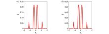
ObjectiveModulation instability is a crucial phenomenon in the study of nonlinear dynamics, where an unstable system results in the destruction of its original states, accompanied by the rapid growth of small perturbation instabilities. The Bose-Einstein condensate serves as an ideal platform for exploring modulation instability due to its precise experimental control over the system's nonlinear dynamics. Therefore, studying modulation instabilities holds profound significance in comprehending the nature of Bose-Einstein condensate systems. In this paper, we reveal that spin-orbit coupling can always introduce modulation instability into a kind of specific state. We call it spin-orbit-coupling-induced modulation instability. The states are specific as they are zero-quasimomentum states. We find that there exist four different zero-quasimomentum states, and we classify them as no-current-carrying states and current-carrying states according to whether the states carry current or not. In literature, modulation instability of the no-current-carrying states has been investigated. The current-carrying states are unique due to their current originating from spin-orbit coupling, and their existence is unstable due to nonlinearity. We find that all these zero-quasimomentum states are modulationally unstable in all parameter regimes. The consequence of such modulation instability is the formation of complex wave structures.MethodsThe properties of modulation instability and the corresponding nonlinear dynamic images are primarily investigated using Bogoliubov de Gennes (BdG) instability analysis and the split step Fourier method. BdG instability analysis is a widely employed technique for analyzing instability in the study of superfluidity and Bose-Einstein condensates. It primarily examines the system's stability and its response to perturbations by solving nonlinear eigenvalue equations. By diagonalizing the BdG Hamiltonian matrix, the eigenvalues can be obtained. The eigenvalues of the matrix may be complex due to the non-Hermitian nature of the BdG Hamiltonian. If one or more complex numbers exist in the eigenvalues, the state becomes unstable. Consequently, any imposed disturbance experiences exponential growth, leading to the instability of the state. In addition, the split step Fourier method is commonly used for handling time evolution. The underlying principle of this method is to separate the terms of the system Hamiltonian and process them individually. The key step involves employing distinct treatments for the nonlinear and linear terms of the equation to be solved.Results and DiscussionsInitially, we investigate the case of g>g12 and observe that the system exhibits a four-band modulation instability image in Fig. 1. Among these bands, the two branches positioned near the lower quasi-momentum region are referred to as the primary modulation instability band, while the two branches near the higher quasi-momentum region are known as the secondary modulation instability band. Notably, it is determined that identical chemical potentials of the two current-carrying states yield the same modulation instability image. Furthermore, we perform calculations to ascertain the nonlinear dynamic images (Figs. 2 and 3). The investigation reveals that the density evolution of the two components follows similar ways, exhibiting trends of movement in both positive and negative directions along the x-axis. As time progresses, both components undergo chaotic oscillations. In the quasi-momentum space, distinct motion trends and reversal symmetry are observed between the two components. After a certain period of evolution, significant separation occurs. This phenomenon arises from the modulation instability being predominantly influenced by different modulation instability bands at various stages. Initially, the primary modulation instability band dominates, while in later stages, the secondary modulation instability band takes control. Ultimately, the system tends to approach the quasi-momentum space of the secondary modulation instability band, leading to chaotic propagation. Simultaneously, we also examine the scenario where g<g12 and observe that the system's modulation instability image consists of only two bands (Fig. 4): the primary modulation instability band. This disappearance of the secondary modulation instability band occurs as the repulsive interaction between the components intensifies, causing the two unstable branches to merge. Following a nonlinear dynamic analysis (Figs. 5 and 6), we observe that the motion trends become less pronounced due to the absence of the secondary modulation instability band. Nevertheless, in this case, the two components still exhibit distinct motion patterns and maintain reverse symmetry. The reason behind this phenomenon remains consistent with the previous situation. However, since there are only two branches of modulation instability, the system consistently resides near the quasi-momentum space of the main modulation instability band once the wave function enters chaotic oscillation.ConclusionsWe delve into the examination of modulation instability and its consequential dynamic patterns in one-dimensional two-component Bose-Einstein condensates with spin-orbit coupling. The study reveals the existence of four distinct zero momentum states within the system, where two of them carry currents while the remaining two do not under specific conditions. It should be noted that the generation of these four states is not solely determined by spin-orbit coupling; however, the presence of spin-orbit coupling does impact the modulation instability of the system. Previous research predominantly focuses on the zero quasi-momentum state without current carrying, neglecting the investigation of the zero quasi-momentum state with current carrying. We specifically explore the modulation instability of current-carrying zero momentum states. The findings indicate that in the presence of Rabi coupling, when the intra-component interaction surpasses the inter-component interaction, the modulation instability image manifests four branches, consisting of two main modulation instability bands and two secondary modulation instability bands. Conversely, when the intra-component interaction is lower than the inter-component interaction, the modulation instability image presents only two branches. We also establish a correlation between modulation instability and the nonlinear dynamic evolution of the system. Additionally, the presence of modulation instability can trigger the emergence of intricate patterns.
ObjectiveFiber Fabry-Perot tunable filters (FFP-TF) controlled by piezoelectric ceramics are prone to temperature drift in fiber Bragg grating (FBG) sensing systems. During the long-term measurement process, FFP-TF will cause continuous drift of the output wavelength, which will adversely damage the FBG sensing system's measurement accuracy. At the moment, FFP-TF temperature drift compensation primarily entails adding hardware calibration modules to the FBG sensing system, such as the reference grating method, F-P etalon method, gas absorption method, and composite wavelength reference method. Although these technologies can efficiently adjust for temperature drift, they greatly increase the system's cost and complexity. As a result, utilizing software approaches to compensate for temperature drift in FFP-TF is a practical and low-cost method. However, most contemporary temperature drift compensation approaches based on artificial intelligence technologies neglect temperature drift data's temporal features. In fact, the fresh sample has a higher impact on the prediction outcomes of the following data than the old sample. As a result, this work extensively addresses the impact of temporal features on temperature drift compensation when processing temperature drift and other highly time-dependent data. A tunable filter temperature drift compensation approach with time weight is suggested based on the AdaBoost-SVM algorithm and time weight.MethodsWe use FBG0 as the reference grating and the other three FBGs as sensing gratings, and each sensing grating is modeled individually. The temperature-related values of the experimental environment are chosen as the model's input features in this investigation. Furthermore, because the wavelength drift errors of each FBG in the FFP-TF output spectrum have a high correlation, we use the drift of the reference grating as an input feature of the dynamic compensation model to compensate for the lack of accurate temperature information in the F-P cavity. The significant link between the temperature drift sequence data before and after is taken into account in full by this investigation. The idea of time weight is introduced in the process of modeling the temperature drift of FFP-TF to assign various temporal attributes to each sample. After that, temperature drift samples are modeled using support vector machines (SVM) as weak learners, and several SVM learning models are integrated using the AdaBoost framework. In the integrated prediction process, the time attribute of samples has an impact on the update of sample weights in addition to the prediction performance of each model. Multiple temperature change modes have been used to validate the aforementioned procedure.Results and DiscussionsFirst, the temperature drift compensation results of the proposed algorithm are compared with the conventional AdaBoost-SVM algorithm for three transmission gratings in the 2 ℃ narrow changing temperature environment experiment of cooling and heating (Table 3). Secondly, in the 15 ℃ cooling amplitude experiment, the temperature drift compensation results of the proposed algorithm are compared with the traditional AdaBoost-SVM algorithm for three transmission gratings. The experimental results show that the maximum temperature drift compensation error of the traditional AdaBoost-SVM algorithm is 10.83 pm, while the maximum temperature drift compensation error of the AdaBoost-SVM based on time weight is reduced to 7.04 pm. The results show that the classic AdaBoost-SVM algorithm's maximum error is approximately 11.57 pm, whereas the maximum error of the AdaBoost-SVM based on time weight is only approximately 4.05 pm. The strategy suggested in this research, however, outperforms unoptimized machine learning methods in terms of superior stability, stronger reliability, and higher prediction accuracy (Table 4). The aforementioned findings show that the method suggested in this article may successfully determine samples' temporal properties, allowing for more reasonable sample weight allocation, a decrease in model performance fluctuations, and an increase in model accuracy.ConclusionsFirst, the high link between the temperature drift sequence data before and after is thoroughly taken into account in this article. The ratio of new and old samples is altered by applying various new weights at various time points, which makes the distribution of sample weights more logical and enhances the model's performance. The experiment next establishes a nonlinear model between the filter surface temperature and output drift error using the spectral locations of three reference gratings as input features. Experiments are carried out on two datasets with different temperature change patterns, and the results reveal that the first dataset does not fully comply with the more important rule of closer samples in general time series proposed in this article due to the short-term fluctuation of temperature changes, so the performance improvement of the model is not significant; the temperature change in the second dataset demonstrates a monotonic cooling trend with apparent gradients, which is more consistent with the more important principles of closer samples, and the performance gain is more significant. Unlike typical hardware techniques, the method suggested in this paper does not require any additional hardware, resulting in a novel approach to temperature drift compensation of tunable filters.
ObjectiveAlthough visible light communication has become a research hotspot, its development continues to focus on how to improve the transmission rate, transmission distance, and equipment utilization. The development of metal organic chemical vapor deposition technology leads to micro-light-emitting diodes (micro-LEDs) and other high-performance Ⅲ‑nitride devices. Compared with the white commercial LEDs, the micro-LED has the advantage of high modulation bandwidth, high brightness, and low coherence in the visible light communication (VLC). A variety of optical wireless transmissions using multiple quantum well LEDs or photodetectors has recently been reported. Considering that miniature high-speed visible light communication using LEDs is a potential complementary technology for dual-functional wireless communication network towards 6G, we propose that GaN-based multiple quantum well (MQW) diodes on the silicon substrate can simultaneously emit and detect light, which in practice can perform transmitting devices and receiving devices simultaneously in the VLC.MethodsBased on the schematic of the cross-sectional structure of the InGaN/AlGaN diodes, we design and fabricate a Si-substrate micro-ring light-emitting diode (MR-LED) using a standard semiconductor process. We begin by evaluating the photoelectrical performance and communication performance of MR-LED. The optoelectronic characteristics of the MR-LED including I-V relation, electroluminescence, and the response curve of the LED are measured by an Agilent Instrument B1500A source meter and an Oriel Instrument IQE-200 B quantum efficiency system. Subsequently, for characterizing the communication performance, we propose out-of-plane visible light communication where a Hamamatsu C12702-11 photodiode module detects spatial modulated light emission by MR-LED, and the MR-LED pluses its light in coded pseudorandom binary sequence signals or carries image information. The photogenerated electron-hole pairs lead to an induced photocurrent when we employ a 375 nm and 20 mW laser beam to illuminate the MR-LED. We extract the signals detected by MR-LED. When the diode is turned on with external illumination, the measured current is a summation of the driving current and photocurrent. In this situation, the diode simultaneously emits and detects light. When appropriately biased and illuminated, the induced photocurrent is distinguishable from the driving current. We can then extract the photocurrent signal for analysis and implement a spatial full-duplex communication system.Results and DiscussionsAccording to the photoelectrical performance of MR-LED, the turn-on voltage of the diode is 2.8 V, and the dominant EL peak is measured at approximately 379.4 nm and an injection current of 5 mA. The overlap area between the luminescence spectrum and the detection spectrum of the MR-LED is 20 nm, which proves that the communication system of simultaneous light transmission and light reception is feasible from an optical point of view (Fig. 4). The MR-LED is observed to provide a -3 dB frequency response exceeding 66.8 MHz, and thus is suitable for high-speed VLC. The external photodiodes detect the spatial light emission to convert the photos back into electrons at a rate of 150 Mbit/s. The KEYSIGHT DSOS604A digital storage oscilloscope shows resolved eye diagrams at the rate of 150 Mbit/s (Fig. 5). In optical wireless image transmission systems, MR-LED emits signals carrying the image information. The signal received by the photodetector is amplified and then restored in MATLAB, and an eye diagram is displayed on the oscilloscope (Fig. 6). As a receiver, the MR-LED based on negative voltage of -2 ,-4,and -6 V detects the 375 nm laser modulated light signal. The received signal amplitude is around 150, 280, and 350 mV respectively. Therefore, the higher negative bias voltage loaded on the MR-LED leads to better detection performance of the MR-LED. When biased at 4.15 V, the diode as a receiver operating in the simultaneous emission-detection mode can still receive different frequency laser signals. As the frequency of the external light signal increases, the amplitude of the received signal is distorted when the MR-LED is emitting light. The amplitude of the received signal increases from 38.8 mV to 110.8 mV as the Vbias rises from 3.85 V to 4.15 V (Fig. 7). Above the turn-on voltage of 2.8 V, the increase in the biased voltage slightly influences the amplitude of the received signals. The results show that the MQW-diode can sense light in either the detector or emitter mode, indicating the possibility of spatial full-duplex communication using visible light.ConclusionsWe propose, fabricate, and characterize GaN-based MQW diodes with micro-ring geometry. Due to the spectral overlap between the emission and absorption spectra, a multifunctional MR-LED allows light emission and detection simultaneously. As a transmitter, the MR-LED demonstrates out-of-plane data transmission at 150 Mbit/s using on-off keying modulation. The optical wireless transmission of image data is also implemented by software processing. As a receiver, whether illuminated or not, the MR-LED can detect free-space optical signals under different bias voltages. The realization of space full-duplex communication shows that the multi-functional MR-LED can reduce material costs and processing costs in a miniature high-speed VLC system.
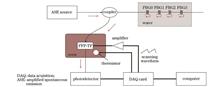
ObjectiveDuring shale gas exploitation, a distributed optical fiber acoustic sensing system (DAS) based on phase-sensitive optical time domain reflectometry (Φ-OTDR) is a commonly employed solution for monitoring microseismic waves generated during hydraulic fracturing operations. Signal-to-noise ratio (SNR) is an important parameter reflecting the performance of the Φ-OTDR system, and obtaining microseismic signals with good SNR is the basis for monitoring the fracturing effect of shale gas. However, due to the thermal noise and scattering noise of the photodetector, the phase noise and frequency drift of the laser, and the environmental noise, the SNR of the Φ-OTDR system will deteriorate, resulting in difficult vibration localization and distorted phase signal obtained by demodulation. The solution to this problem is essential for broad applications of Φ-OTDR systems in the engineering field.MethodsTo improve the SNR of vibration signals measured by Φ-OTDR systems, we propose a vibration signal denoising method based on variational mode decomposition (VMD) and mutual information (MI). The in-phase orthogonality (I/Q) demodulated phase signal is further processed, and the number of VMD layers K is determined by the scaling index calculated by detrended fluctuation analysis (DFA). The process of the DFA method is as follows. First, the input noisy signal is decomposed into K(K=1,2,3…) IMF components by VMD, and then the scaling index of each mode is estimated by DFA. The relationship between the number of decomposition layers K and the scaling index is K=argmaxKnum(α1:K≥θ)=J,K=1,2,3,⋯, where the parameter Jis determined by the scaling index of the input noisy signal. When the value of K is determined, the MI between the IMF components generated by the K-layer VMD and the input noisy signal is calculated. The mean value of the normalized MI of each component and the input signal is taken as the threshold value. Additionally, when the normalized MI of a component and the input signal is greater than this threshold value, the component is considered to be a correlated mode, otherwise it is a non-correlated one. The distortion and noise of the phase signal are suppressed by discarding the non-correlated modes determined by the MI method.Results and DiscussionsA coherent detection Φ-OTDR system is set up to verify the denoising effect of the VMD-MI method. The 500 Hz single-frequency vibration signal (Fig. 6) and the 500, 1000, and 1500 Hz multi-frequency vibration signals (Fig. 10) are processed by VMD, wavelet denoising (Wavelet), empirical mode decomposition (EMD), and complete ensemble empirical mode decomposition with adaptive noise (CEEMDAN). For the 500 Hz single-frequency vibration signal, the number of decomposition layers K is determined as 4 by the DFA method, and the MI between each component and the original phase signal is calculated (Fig. 7) to determine IMF3 as the correlated mode to be retained, and the remaining components are discarded as non-correlated modes. For the original phase signal with the SNR of 18.34 dB (Fig. 6), the proposed method improves the SNR to 41.45 dB, which is significantly better than the 18.46, 34.87, and 38.60 dB of the Wavelet, EMD, and CEEMDAN methods, respectively (Fig. 8). For the multi-frequency vibration signals of 500, 1000, and 1500 Hz, the number of decomposition layers K is determined to be 7 by the DFA method, and the IMF3, IMF4, IMF5, and IMF6 are determined to be correlated modes and the remaining components are non-correlated modes by the MI method (Fig. 9). Meanwhile, the noise reduction is reduced by discarding the non-correlated modes. For the original phase signal with SNR of 18.82, 20.38, and 17.41 dB, the proposed method improves the SNR to 32.28, 33.77, and 30.68 dB respectively, significantly better than Wavelet, EMD, and CEEMDAN methods (Fig. 10).ConclusionsThe DAS system based on Φ-OTDR is a promising detection device in the microseismic monitoring of shale gas fractures. The SNR is an important criterion to evaluate the quality of the detection signal, and enhancing the SNR is significant to improve the overall sensing performance of the DAS system. We propose a method to improve the SNR of Φ-OTDR based on VMD. The DFA method is adopted to determine the appropriate number of decomposition layers, and the correlated modes are selected and retained by calculating the MI between the components obtained from VMD and the original phase signal to achieve noise removal. The experimental results show that the VMD-MI algorithm is significantly better than Wavelet, EMD, and CEEMDAN in improving the SNR of 500 Hz single-frequency vibration signal, and 500, 1000, and 1500 Hz multi-frequency vibration signals. This proves the effectiveness and superiority of the proposed method in improving the measurement performance of the Φ-OTDR system. Meanwhile, this method can help acquire high-fidelity microseismic information in microseismic monitoring of shale gas.
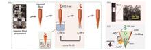
ObjectiveSurface-enhanced Raman scattering (SERS) is a powerful analytical tool that can provide molecular vibrational fingerprint information. Due to its unique analytical advantages, SERS has been widely applied in various fields such as biomedical research, environmental monitoring, and food analysis. During the development of SERS technology, silver nanoparticles have often been used as SERS substrates due to their excellent localized surface plasmon resonance properties. However, their susceptibility to oxidation poses a significant limitation in the construction of nano-probes for practical applications. In contrast, gold nanoparticles have better chemical stability and lower biotoxicity but relatively weaker Raman signal enhancement capability. Therefore, bimetallic SERS substrates combining gold and silver are characterized by high sensitivity and stability. Compared with traditional substrates, tapered optical fibers not only have the advantages of in-situ detection and remote signal transmission but also have great potential for enhancing laser reflection and improving light collection capability, which is beneficial for collecting weak Raman signals and achieving lower detection limits. Therefore, we proposed a simple and cost-effective bimetallic tapered optical fiber SERS probe. This probe utilized a light-induced method to deposit gold and silver nanoparticles on the surface of the tapered optical fiber, providing high sensitivity and good stability.MethodsThe bimetallic tapered optical fiber SERS probe was prepared by using a light-induced method in this study. First, the tapered fiber was prepared by using the fiber fusion tapering machine. After clamping the processed fiber onto the fiber holder, the fiber fusion tapering machine was started to initiate the tapering process. Once the machine stopped operating, two tapered optical fibers were obtained. Second, gold and silver nanoparticles with an approximate diameter of 50 nm were prepared by using a chemical reduction method. Finally, the bimetallic tapered optical fiber SERS probe was prepared through the light-induced method. The laser beam emitted by a helium-neon laser was coupled into the tapered optical fiber. Subsequently, the tapered end was immersed in a mixed solution of Ag sol and Au sol (volume ratio of 1∶1, both 0.3 mL) for 60 seconds. Then, the tapered end was moved from the solution to the air and kept in that position for 90 seconds while the laser was still operating. This process was repeated 15 times [Fig. 1(a)]. At the end of the entire procedure, the bimetallic tapered optical fiber SERS probe was obtained. The surface morphology of the tapered optical fiber was characterized by scanning electron microscopy (SEM), and the performance of the optical fiber probe was tested by a confocal Raman spectrometer.Results and DiscussionsIn this study, SEM analysis [Fig. 2(a1) and (a2)] of the prepared samples revealed a uniform distribution of metal nanoparticles on the fiber surface, exhibiting a mostly monolayer arrangement. The relative mass percentages of Ag and Au elements were found to be 2.36% and 9.21%, respectively [Fig. 2(b) and (c)]. The average particle size of the metal particles on the sample was 49 nm, with an average gap of 6.8 nm [Fig. 2(e1) and (e2)]. In the paper, Rhodamine 6G (R6G) was selected as the analyte molecule to evaluate the SERS performance of the prepared samples. The bimetallic tapered optical fiber SERS probe was immersed in R6G solutions with concentrations ranging from 10-8 to 10-10 mol/L for three minutes respectively. After removal from the solution and natural drying, Raman signal detection was performed, and the obtained enhancement factor (AEF) for the samples reached 2.07×10⁸. To demonstrate the capability of detecting non-single molecule analytes, the samples were immersed in a mixed solution of 10-6 mol/L R6G and 10-4 mol/L crystal violet (CV) for three minutes. After removal from the solution and natural drying, the detection was conducted, and the results indicated that the unique Raman peaks of different probe molecules could be detected in the mixed solution [Fig. 6(b)]. To demonstrate the excellent stability of the bimetallic tapered optical fiber SERS probe, it was placed for different durations of 24 hours, 48 hours, 72 hours, and 96 hours. Afterward, a comparison was made by using Raman testing of 10-7 mol/L R6G. The results indicated that the sample exhibited good stability (Fig. 7).ConclusionsIn this study, to enhance the enriched density of metal nanoparticles on the surface of optical fibers and improve the stability of the Raman-enhancing properties of the optical fiber SERS composite structure, we proposed a bimetallic (gold and silver) tapered optical fiber SERS probe structure. First, gold and silver nanoparticles with uniform morphology were prepared using the chemical reduction method. Then, the bimetallic particles were enriched on the tapered optical fiber using light-induced methods. The prepared optical fiber SERS probe exhibited excellent experimental performance. In this study, the lowest detected concentration of R6G was as low as 10-10 mol/L, and the enhancement factor was 2.07×10⁸; compared with single-metal silver optical fiber SERS probes, the stability of the bimetallic sample was improved by seven times (after 96 hours). The bimetallic tapered optical fiber SERS probe is expected to be applied in in-situ and remote detection in the future. The next research direction is to explore the key process of controllable double metal modified optical fiber, so as to further optimize the detection sensitivity and stability of the sample.
ObjectiveThe rapid evolution of bionic flexible tactile sensors is driven by the overarching goal of emulating human tactile perception to augment robots' perceptual acuity. Conventional electric sensing paradigms grapple with a myriad of challenges, including elevated manufacturing costs and susceptibility to signal interference. Meanwhile, due to the small size, strong flexibility, and high sensitivity, optical sensing modalities are pushing micro/nano fibers (MNFs) into the spotlight. Domestically, the Zhejiang Lab is at the forefront of developing various MNF-based sensors, enabling single/dual-modal detection for applications in human-machine interaction and physiological parameter monitoring. Nevertheless, the challenge of balancing sensitivity and operational range remains unresolved in current methods, compounded by susceptibility to wear-related issues. Thus, we introduce a micro/nano fiber-based flexible tactile sensor unit inspired by fingertip skin microstructures (FIMF). By simulating the biological microstructures and tactile conduction mechanisms of fingertip skin, FIMF achieves the detection of mechanical stimuli and object feature recognition. The advanced sensor structure and functional attributes are significant for applications in flexible bionic devices and advanced robotics technology.MethodsFirstly, the proposed flexible tactile sensing unit FIMF is inspired by the microstructure of fingertip skin and is achieved by embedding an MNF between two layers of polydimethylsiloxane (PDMS) films. The structure is further enhanced by introducing two layers of elastic resin annular ridges on the surface, each with varying stiffness. This design aims to replicate the intricate microstructure of biological fingertip skin and its underlying tactile conduction mechanism. Subsequently, we delve into the influence of PDMS film thickness and the dimensions of the annular ridges on the tactile pressure response of the FIMF sensor. Based on meticulous simulation results, the optimal sensor parameters are identified with a PDMS film thickness of 50 µm, an upper annular ridge thickness of 0.2 mm, and a lower annular ridge thickness of 0.4 mm. Furthermore, we extensively examine the FIMF sensor's response to diverse tactile stimuli, including static and dynamic pressure, and vibrations. Finally, the FIMF's ability to discern object hardness and surface textures is investigated by employing a synergistic approach integrating the mechanical finger's travel distance and the FIMF force feedback to discern object hardness characteristics. Meanwhile, we conduct waveform analysis of transmitted intensity changes over time to perceive and compute object texture. The pursuit of further insight into different textures is accomplished by the application of short-time Fourier transform (STFT) to extract frequency domain features.Results and DiscussionsThe experimental findings underscore that the devised FIMF inspired by the microstructures of fingertip skin presents an amalgamation of wide-ranging dynamic detection capabilities and high sensitivity. Remarkably, it boasts response and recovery times of less than 100 ms, providing the sensor with the capacity to swiftly discern mechanical stimuli (Fig. 7). Furthermore, the sensor exhibits exceptional robustness and elevated static/dynamic stability, which is a testament to the robust encapsulation of its diverse structural layers (Fig. 8). Expanding its sensing range is proven instrumental in significantly enhancing the sensitivity for minute pressure ranges (0-2 N), thereby achieving an enhancement of approximately fourfold compared to recently reported MNF tactile sensors. A pivotal facet arises from the microstructure integration to amplify tactile mechanical stimuli and translate them into MNF deformations. This innovative approach does not need to employ tapering processes that would require reducing the MNF diameter to below 2 µm, which not only streamlines manufacturing but also augments the overall structural resilience (Table 1). In object hardness/texture perception, the FIMF divulges a pertinent trait that the transmitted intensity diminishes with the escalating hardness. This phenomenon arises because stiffer objects induce greater forces and stresses during contact, thus culminating in a more conspicuous attenuation of optical intensity (Fig. 9). The FIMF employs a spatial frequency-based characterization for discerning object texture, and the texture wavelength is derived by dividing the sliding speed by the dominant frequency. Additionally, the STFT of the transmitted light intensity signal provides a richer depiction of intensity fluctuations over time. During scans across regular surface patterns, the light intensity signal engenders periodic motifs at frequencies below 10 Hz. Notably, the number and positioning of these motifs amplify in tandem with increased scanning speeds in the temporal domain (Fig. 11).ConclusionsWe propose a novel micro-nano optical fiber flexible tactile pressure sensor inspired by the fingertip skin microstructure. This sensor combines force sensing with object hardness/texture detection capabilities. The sensor's force conduction performance is enhanced by bionic design to offer a wide detection range (0-16 N), high sensitivity (20.58% N-1), short response time (86 ms), extended lifespan, and low cost. By demonstrating its functionality, we directly connect this soft sensor to a robotic manipulator, enabling it to differentiate between soft and hard objects, perceive object textures, and measure gripping forces. Consequently, this sensor is suitable for robotic gripping operations. Thus, the proposed sensor possesses structural and functional features reminiscent of human fingertip skin and has promising potential for applications in bionic artificial skin and advanced robotics technology.
ObjectiveDue to its non-invasive, high-resolution, and real-time imaging capabilities, optical scanning microscopy has been widely applied in biomedicine, physical chemistry, and materials science to realize three-dimensional imaging detection of cells, tissue analysis, and microstructure samples. Beam scanning systems play an important role in optical microscopy. When scanners are leveraged for scanning and imaging, it is necessary to add a relay system composed of a scan lens and tube lens between the scanner and the objective lens. As a result, the beam does not deviate from the rear pupil of the objective lens to ensure the imaging quality. However, traditional relay systems adopt lenses design, and their inherent defects can cause optical aberration, which affects the resolution of optical microscopy imaging systems. Commercial scan lens and tube lens are optimized to suppress aberrations, but they feature high price, large volume, and long focal length, making them unsuitable for miniaturized design occasions. The relay system composed of doublet lenses can be miniaturized according to requirements, but it is difficult to effectively suppress aberrations, especially under large beam scanning angles. The utilization of parabolic reflectors to form a relay system can effectively eliminate the chromatic aberration, but the coma aberration of the reflection system is difficult to eliminate. This is the same as the lens relay system, which requires a one-to-one correspondence of the focal position and high installation accuracy. Therefore, how to design aberration-free beam scanning systems with miniaturization and simple structures is still an important problem facing optical microscopy imaging technology.MethodsAiming at the large size, large aberration, and high alignment accuracy of the relay systems in existing beam scanning systems, we propose a dual two-dimensional (2D) MEMS mirror beam scanning method. This method adopts two 2D MEMS mirrors to realize beam telecentric scanning. One mirror replaces the scan lens and tube lens in the traditional relay system to avoid the introduction of aberrations, reduce the system size, and finally design an aberration-free beam scanning system with miniaturization and simple structures. There is a one-to-one correspondence between the scanning angle of the scanning beam and the tilt angle of the MEMS mirrors. By controlling two MEMS mirrors to cooperate with different tilt angles, this method can make the excitation beam arrive the rear pupil of the objective lens at different angles to complete the 2D lateral scanning.Results and DiscussionsTo obtain the relationship between the angle of the scanning beam and the deflection angle of the two MEMS mirrors, we build a mathematical model of the dual 2D MEMS mirror scanning system, and analyze it in detail. First, the relationship between the tilt angle of the MEMS mirror and the beam scanning angle is analyzed. Under different d/l ratios (with dbeing the distance between two MEMS mirrors,and l being the distance between the second MEMS mirror and the rear pupil of the objective), the tilt angle of the MEMS mirror and the beam scanning angle have different relations. It is found that the dual 2D MEMS mirror scanning system can achieve a large angle beam scanning by adjusting the d/lvalue when the deflection angle of the first MEMS mirror is constant (Fig. 4). Additionally, the values of d and l can be selected arbitrarily, which is flexible in design and convenient for system miniaturization. Then, the aberrations of the traditional relay system and the dual 2D MEMS mirror scanning system are analyzed by Zemax optical design software, and their performances are compared. According to the simulation results, the dual 2D MEMS mirror scanning system avoids the introduction of aberrations and has better imaging quality than the traditional relay system (Figs. 6-7). Meanwhile, the system structure is simple, easier to adjust, and can avoid the influence of installation error on the system (Fig. 10). Finally, based on this method, a miniaturized confocal scanning microscope is constructed, and the step sample is utilized to obtain the height and period information of the sample (Fig. 13), which verifies the feasibility of the method.ConclusionsWe propose a dual 2D MEMS mirror beam scanning method, which leverages a 2D MEMS mirror instead of the traditional relay system to design an aberration-free beam scanning system. In addition, the dual 2D MEMS mirror structure has no requirements for the focus position, making it convenient for miniaturization design and installation. A dual 2D MEMS mirror scanning confocal microscope is constructed based on this method, and the feasibility of this method is verified by testing standard step samples. This method provides a new beam scanning approach for optical microscopy, which is of great significance for optical microscopic systems with strict aberration requirements such as confocal microscopes, two-photon microscopes, optical coherence scanning microscopes, and chromatic confocal microscopes.
ObjectiveThe action of implementing computational photography for targets out of the field of view (FOV) such as behind the barrier by a reflective relay surface is defined as non-line-of-sight (NLOS) imaging. NLOS technology has a promising future in the fields of medicine, road safety, and scientific research due to its ability to expand the human's FOV in scenarios where a direct view is impossible to obtain by devices or human eyes. The present NLOS technology mostly includes transient imaging, range-gated imaging, and passive pattern imaging, and they are mostly dedicated to Lambert reflector relay surfaces. However, the materials in common scenarios are usually non-Lambertian reflectors, whose scattering characteristics are random and diverse, with different degradation characteristics of NLOS imaging results. The traditional methods always have complex system structures, slow imaging speeds, and high costs. We propose a new NLOS method based on the time of flight (TOF) camera, which requires lower maintenance costs, indicates higher availability than the transient imaging and range-gated imaging, and can also realize 3D reconstruction compared with the passive pattern. The NLOS 3D imaging can be achieved for the relay surface with non-Lambertian scattering characteristics by the proposed method to provide theoretical references and an experimental basis for the application.MethodsThe NLOS images collected by the reflective relay surface suffer from serious degradation of which the process is directly determined by the optical scattering characteristics of the relay surface. The following theoretical hypothesis is provided by analyzing the propagation method of the target optical signal (Fig. 1). The degraded images are formed from convolution between the clear image and the relay surface with scattering characteristics. As a result, reconstruction for clear images can be realized through the deconvolution of degraded images if scattering characteristics of the relay surface are obtained. Depth imaging can be achieved for the TOF camera by calculating the phase differences between the incoherently modulated illumination and the returned light signal from targets. The phase difference calculation relies on the signal intensity, and the relay surface scatters the optical signal and degrades the depth image. Therefore, the implementation method of the reconstruction algorithm is as follows. First, scattering characteristics of the relay surface are obtained with the genetic algorithm (GA) through clear and degraded images respectively of the given target. Second, clear images are reconstructed through deconvolution for degraded images of other targets based on the above scattering characteristics. Finally, the pixel value of the depth image for the TOF camera is the floating number which is different from common 2D images. Thus, most of the traditional imaging method evaluation is unsuitable for depth evaluation. A kind of difference image is employed for subjective evaluation and mean square error (MSE) for objective evaluation.Results and DiscussionsWe put forward an NLOS depth imaging method based on the TOF camera. The scattering characteristics of the relay surface should be solved first to realize the reconstruction through deconvolution. However, the scattering characteristics of the relay surface are completely unknown in the NLOS mathematical model. For any of two different materials (Fig. 5), several different scales of matrices are adopted to express them in the algorithm, while the GA calculates matrix value by the fitness function [Eq. (8)]. The results are approximate numerical values of scattering characteristics of the relay surface (Fig. 7), and the 2D matrix with minimum fitness is set to be the deconvolution kernel. Then reconstruction is conducted for degraded NLOS depth images of the unknown target by Lucy-Richardson (LR) deconvolution. The experimental results reveal the effectiveness and feasibility of the algorithm both from subjective and objective evaluation (Figs. 8 and 9), but the results are not always convergent without complete expression of scattering characteristics in the 2D matrix. Although the solving process takes a long time, the calculated matrix of scattering characteristics can be applied. However, the GA-LR algorithm provides a low-cost NLOS 3D imaging technique, which can be directly applied to practical scenarios if the scattering characteristics database of common materials is established in advance. Therefore, the proposed method both provides theoretical guidance and an experimental basis for NLOS imaging, and also provides solutions to practical problems, with economic significance.ConclusionsBased on a TOF camera, we propose a 3D imaging method for NLOS targets. By analyzing the optical phenomena, we put forward a hypothesis that the degraded 3D image results from the clear 3D image convolution with some unknown scattering process, where the unknown scattering process is caused by the relay surface. Therefore, the GA is adopted to solve the approximate optical model of the relay surface, and then the LR deconvolution algorithm is to perform the 3D reconstruction of NLOS targets. The experimental results show that the NLOS targets are well reconstructed from both subjective and objective aspects. In practical applications, after the approximation model of the relay surface is determined, this algorithm can quickly capture the NLOS target and perform 3D imaging when a TOF camera is utilized, which indicates high application significance. In the future, deep neural networks may be leveraged to fit the degradation process to realize reconstruction.
The proposed method adopts a Fourier single-pixel imaging algorithm that includes a differential operation to enable the suppression of out-of-focus background noise. However, due to the utilization of single-pixel imaging, the measurement number of the proposed method is more than that of the traditional multi-mode microscopic imaging method. Through taking the experimental results in our paper as an example and employing Intel(R) Core(TM) i7-10700 CPU @ 2.90 GHz, 32.0 GB memory, it takes about 4 min to reconstruct four multi-mode images with a pixel count of 850×850, and the calculation time depends on the image number of pixels. Therefore, the proposed method is not suitable for dynamic imaging scenes.ObjectiveIn the manufacturing of micro-nano devices such as semiconductor chips, their morphology characterization is helpful for manufacturing process evaluation and defect detection. To obtain complete information on the sample to be tested, one has to use bright field microscopes and dark field microscopes for joint characterization of multiple imaging modes. However, the existing methods to achieve multi-mode imaging need to change the experimental device or adopt a different imaging system, which leads to different fields of view of the acquired multi-mode images and is not conducive to comprehensively analyzing the samples to be tested by synthesizing the multi-mode imaging results. Therefore, it is necessary to develop multi-mode microscopic imaging technology to deal with the above problems. For example, microscopes based on LED array light source and multi-mode microscopic imaging technology using spatial light modulators are utilized to perform different filtering in the spectral plane of traditional microscopes.MethodsOur paper proposes a multi-mode microscopic imaging technology based on the single-pixel imaging principle. It employs wide-field structured light to encode the spatial information of the sample and then leverages each pixel of the camera as a single-pixel detector to reconstruct an Ariy image. Different points on the Airy disk image correspond to different orders of signals diffracted by different object points. Therefore, by designing different digital pinholes to extract the values at different positions on the Airy disk image and arranging them according to the camera pixel coordinates, multi-mode images can be reconstructed, such as bright field images, bias images, and dark field images.Results and DiscussionsTo design the digital pinhole to extract the signals of different diffraction orders of the sample, we should calibrate the conjugate relationship between the camera and the pixels of the spatial light modulator. We adopt an affine matrix to represent the correspondence between the camera and the spatial light modulator, and the calibrated reprojection error is shown in Fig. 7. After the affine matrix is calibrated, digital pinholes can be generated according to the calibrated affine matrix. The proposed method is employed to perform multi-modal imaging on a circuit chip and obtain the multi-modal results shown in Fig. 10. However, due to the directionality of digital pinholes, the reconstructed multimodal results are also anisotropic. To obtain isotropic multi-mode results, we design digital pinholes with the same radius and different directions as shown in Fig. 12 to obtain multiple images and then synthesize these images to obtain isotropic results. The isotropic multi-mode results are shown in Fig. 13. We have also verified through the resolution board experiment (Fig. 14) that the contrast of the bright field images reconstructed by extracting the bias signals is higher than that of the bright field images constructed by extracting the zero-frequency signals.ConclusionsOur paper proposes a multi-mode microscopic imaging technique based on the single-pixel imaging principle. It adopts each pixel of the camera as a single-pixel detector to reconstruct an Airy disk image, and the values at different positions in the Airy disk image represent different orders of signals diffracted by different object points. The experimental results show that this technology does not need to change the experimental device or replace different microscopes. By designing different digital pinholes, the light intensity values at different positions can be extracted from the single-pixel reconstructed Airy disk images. These light intensity values correspond to different orders of diffraction signals from different object points. By arranging these extracted signals according to the camera pixel coordinates, images of different modes can be reconstructed, such as bright field imaging, bias imaging, and dark field imaging. The fields of view of these multi-mode images are the same, which is conducive to the comprehensive analysis and acquisition of the complete shape characteristics of the samples. As a new computational imaging method, the proposed method is expected to be applied to the offline characterization of micro-nano devices.
ObjectiveThe diagnosis technology of laser-driven inertial confinement fusion (ICF) is an essential research direction to promote the development of controllable nuclear fusion. Specifically, the velocity interferometer system for any reflector (VISAR) is the most extensively employed diagnostic device of ICF, and it is adopted to record one-dimensional wavefront information with picosecond time resolution generated by ICF. However, the information is only confined to the velocity changes of a line on the target surface and cannot provide two-dimensional (2D) velocity field information of all locations on the target surface. A new type of 2D-VISAR diagnosis system is obtained by combining the compressed ultra-fast photography (CUP) system which can implement 2D ultra-fast imaging with line-VISAR and is applied to ICF diagnosis. The compressed 2D images with high time resolution are obtained, and the 2D stripes of time-varying shock waves are obtained by the inversion algorithm. However, the current mainstream inversion algorithms are readily affected by their regularization parameters, with unstable imaging effects. Therefore, we propose a compressed image inversion algorithm based on variable-accelerated generalized alternating projection (GAP) to optimize the CUP-VISAR inversion effect.MethodsWe put forward a novel CUP-VISAR compressed image inversion algorithm. First, considering the strong low-rank and gradient sparsity characteristics of 2D fringe images, low rank (LR) regularization and total variation (TV) regularization are employed as the prior information of image processing, and the problem is transformed into an optimization problem based on double prior constraints of LR and TV. The GAP algorithm is utilized as an iterative solution framework to decompose the objective optimization problem into two sub-problems, and TV and LR are extended to the sub-problems respectively to give full expression to the synergistic effect of double prior constraints. Finally, considering the influence of error accumulation in iterative GAP under chaotic images, the structure of the algorithm is optimized and improved, and the variable-accelerated processing is proposed to reduce iterative error accumulation.Results and DiscussionsIn the simulation experiment, the shock wave velocity recorded by line-VISAR is extracted to generate a 2D simulation image (Fig. 3). Furthermore, the 2D-VISAR simulation fringe image is extended in the time dimension as the original data (Fig. 4), which is encoded, chopped and compressed to obtain a 2D image with 60 compressed frames (Fig. 6). The inversion effect is simulated and contrasted in noise-free and noisy environments. The results show that compared with the existing algorithms, the average peak signal-to-noise ratio of the proposed algorithm is increased by 11.0 dB and the average structural similarity is increased by 11.4% in the case of no noise (Fig. 8). In the case of noise, the algorithm has stable inversion effect and sound anti-noise ability (Table 1 and Fig. 9). In the real experiment, the experimental optical path is set up (Fig. 10), the CUP-VISAR branch system is adopted to obtain coded images and 2D compressed images, and the line-VISAR branch system is leveraged to obtain 1D shock wave velocity data as the experimental control group (Fig. 11). In the CUP system, the DMD coding aperture is 8×8, the stripe camera slit is entirely opened (about 5 mm), and the temporal resolution is 200 ns. Pulse width of the probe is 5 ns, the image detection frame rate is 5 frames/ns, and the pixel size of the compressed image is 349×788, with the number of compressed frames being 25. The results show that compared with the actual compressed images, the proposed algorithm can still invert the 2D shock wave periphery with clear contour (Figs. 12 and 13). The inversion results are transformed into line-VISAR images and the one-dimensional shock wave velocity is extracted for comparison. Compared with that of the line-VISAR shock wave velocity, the maximal relative error of the inversion results of the proposed algorithm decreases from 20.38% to 11.66%, with a reduction of 8.72% (Fig. 15).ConclusionsIn the proposed CUP-VISAR compressed image inversion algorithm, we introduce LR and TV regularization terms according to the characteristics of fringe images and build a double prior constraint optimization model to promote piecewise smoothing and preserve image features and details. Then, we utilize the GAP framework to solve the optimization model iteratively. Finally, we propose a variable-accelerated method to enhance the anti-noise ability of the algorithm for addressing the error accumulation problem caused by noise factors in GAP iteration. The experimental results show that the proposed algorithm performs well in subjective visual and objective evaluation parameters for the inversion quality of CUP-VISAR compressed images. This means that the algorithm can retain image structure details and smooth characteristics, with sound denoising performance, which verifies the feasibility of the proposed algorithm in CUP-VISAR.
ObjectiveWith the vigorous development of technology in optics and semiconductors, transparent devices with smooth surfaces such as high-precision optical glass are widely employed in semiconductor and other fields. During grinding and polishing, optical glass inevitably produces a large number of scratches, pockmarks, bubbles, pollution particles, microcracks, and other defects in the subsurface. Micron/nanoscale subsurface defects will reduce the physical properties of transparent samples such as optical components, and seriously affect the development of processing and manufacturing technologies in optics and semiconductors. How to detect the subsurface defects of transparent optical components with high precision and provide key parameters for the high-precision preparation of transparent optical components has become an urgent problem in optical inspection. Subsurface defect detection technologies include destructive and non-destructive ones. Destructive detection technologies are simple to operate, and can intuitively and effectively observe the detection results, but they will make the test defects and the actual defects different. Therefore, the existing subsurface defect detection methods mainly focus on non-destructive detection technologies, including total internal reflection microscopy (TIRM), optical coherence tomography (OCT), and laser confocal scanning microscopy (CLSM), but these detection technologies cannot take into account both resolution and detection speed. Through-focus scanning optical microscopy (TSOM) is a model-based optical computational imaging method that can achieve non-contact, non-destructive, and fast measurement of three-dimensional nanostructures. TSOM features high sensitivity, simple hardware system, and sensitivity to nanoscale size changes, and it is not limited by the optical diffraction limit and can conduct online detection. To quickly and non-destructively detect subsurface defects of transparent samples, we propose a new method for detecting micronscale defects in the subsurface of optical components by TSOM and explore it in detail.MethodsThe incident light from the halogen lamp source is irradiated to the subsurface of the sample. Scattering occurs where a defect exists and the scattering light is imaged by the objective lens to the CCD target detector. This method is based on traditional light microscopy and equipped with a high-precision piezoelectric ceramic displacement stage to control the Z movement of the sample, with the movement positioning accuracy of 1 nm. A series of optical images of the subsurface defects are obtained at a certain range of defocus positions from above to below the focus point by scanning along the propagation direction of the light field (Z direction). The images series are stacked according to spatial positions to form an image cube (TSOM cube). Then, the image cube is sliced along the Z direction to generate the TSOM image. The TSOM image is processed through data analysis algorithms to obtain three-dimensional information such as size, shape, and position of micronscale and nanoscale structures, and the target is located by the maximum gray value.Results and DiscussionsThe method can be adopted to detect and locate micronscale defects (Fig. 5). As the refractive index of scattered light is different in different materials, compensation and correction of the refractive index are necessary to obtain the actual depth of the defects (Fig. 7). According to the refraction law, the compensation and correction formula for the refractive index can be derived [Eq. (1)]. After TSOM scanning, the actual depth of the subsurface defects can be calculated based on Eq. (1). Experimental comparison and simulation (Fig. 10) show that larger subsurface defects exhibit volume effects. The position of the maximum light intensity corresponding to the defect in TSOM scanning is point p at the intersection of the radius parallel to the optical axis and its tangent (Fig. 11). To accurately determine the depth from the sample surface to the center of the defect, we should add the defect radius to the depth calculated in the TSOM scanning. After the radius correction, the average depth of the defect is 2000.3 μm, with a standard deviation of 2.4 μm and a relative standard deviation of 0.12%. Compared with other measurement methods, the depth deviation is 1.8 μm (Table 2).ConclusionsThe TSOM method can be employed to detect micronscale subsurface defects in transparent glass and locate the defect depth with a relative standard deviation of up to 0.12%. Theoretically, when the absolute depth of subsurface defects is reduced to hundred-microns, the standard deviation of subsurface defect location is only sub-microns. When TSOM is utilized to locate the depth of subsurface defects at the micrometer scale, it is necessary to compensate and correct the refractive index to further improve the accuracy of defect depth location. When the size of the subsurface defect is large, both the simulation and experiment show that the scattering light intensity distribution of TSOM is affected by the volume effect of the defect itself, which has an important influence on the depth of locating the center of micronscale defects.
ObjectiveWith the rapid development of construction and operation scale of infrastructure such as bridges and tunnels, structural safety is becoming increasingly important. Structural health monitoring is a vital issue in structural safety, operation, and maintenance. Displacement monitoring is one of the most fundamental and routine tasks in structural health monitoring. Among various displacement measurement methods, the contact displacement measurement method is conceptually straightforward to implement. However, it requires specific environmental conditions for accurate measurements. The non-contact displacement measurement methods (e.g., level gauges and total stations) have widespread applications in engineering. However, they cannot satisfy the measurement requirement of long-span structures due to the large-scale range and high accuracy requirements. For deformation monitoring of long linear structures like bridges and tunnels, the displacement-relay series camera network method has been proven to be effective. With the increasing number of camera stations, the accumulated error can be caused due to uncertain factors such as feature extraction errors and model simplifications. It is a challenge to reduce the accumulated error of the camera network. Hence, this study aims to suppress the accumulated error effect, consequently enhancing the measurement accuracy of the camera network.MethodsWe first conduct the theoretical analysis to demonstrate the solution conditions for the displacement-relay series camera network method. Before the simulation study, the basic network configuration is defined. Then, the accumulated error effect of the camera network is investigated through numerical simulations. According to the simulation results, we propose a method based on error coefficients to reduce the accumulated error of the camera network. The error coefficient consists of the condition number of the measurement matrix and the station number of the network. Finally, we provide a direct characterization of network measurement errors to enable the investigation of cumulative effects resulting from displacement transmission errors in the camera network. The influence of benchmarks and survey marks' positions, and their numbers on the measurement accuracy of the displacement-relay camera network is thoroughly analyzed. Based on the analysis results, the camera network configuration is optimized, and an optimal distribution pattern for camera stations and mark points is advised. Finally, the feasibility of the proposed method is verified by field experiments.Results and DiscussionsWe initially discuss the fundamental principle of displacement-relay series camera network and the necessity of benchmarks through the derivation of Eqs. (5)-(10), which also paves the way for extending the theoretical model to a complex camera network. In Section 3.1, the accumulated error effect of the camera network is investigated by integrating the theoretical foundation and formula derivation from Section 2. Subsequently, a detailed discussion of the error transmission effect and error suppression method is carried out through numerical simulations for the basic configuration of the series camera network. Next, the influence of network composition parameters on the transmission error is investigated (Figs. 5 and 6). The transmission errors for the distribution positions of all benchmarks and survey marks are studied (Figs. 7 and 10). A theoretical model that reflects the transmission error of the camera network is proposed by introducing the error coefficient as an evaluation index and leveraging the highly linear correlation between the measurement error and the error coefficient [Eq. (18)]. Finally, the proposed error reduction method is verified by the observation data obtained from a long-span cable-stayed bridge.ConclusionsWe focus on the mechanism and suppression methods of transmission error in the displacement-relay series camera networks. The results show that the displacement transmission link of dual-head cameras requires at least two benchmarks. There is a positive correlation among the number of camera stations, settlement amplitude, pitch angle variation, and network transmission error, while there is a negative correlation between the number of measurement marks and network transmission error. The proposed design method of camera network error suppression based on error coefficient can guide network configuration optimization. The measurement error of the camera network is highly correlated with the defined error coefficient, and the smaller error coefficient leads to a smaller measurement error. The camera stations should be placed at benchmarks to suppress accumulated errors. Replacing the mark points at the benchmarks with camera stations shows that the error suppression effect can reach over 60%, but the error suppression effect will weaken as the number of camera stations increases. The actual bridge verification results indicate that the measurement error is suppressed by 69.13%. The mark points are advised to be placed at camera stations to suppress accumulated errors. The simulation results show that this suppression method can optimize the transmission error of the basic configuration network from 2.88 to 1.01 mm. The actual bridge verification results show that the camera error is suppressed from 10.14 to 3.07 mm.
ObjectiveIn recent years, with the development of computer vision, image processing, data fusion, and other technologies, visual measurement has been widely applied in various fields of modern industry. The inertial measurement unit (IMU) has fast response speed, good dynamic performance, and high short-term accuracy, which can well improve the robustness of visual positioning in complex industrial environments represented by large-scale equipment manufacturing sites such as shipbuilding and aerospace. However, traditional filtering-based visual-inertial fusion algorithms maintain the fusion weights of visual and inertial information unchanged. When visual observation conditions are poor, traditional algorithms will greatly reduce the accuracy of visual-inertial positioning. Therefore, in order to solve the problems of low accuracy, poor adaptability, and low robustness caused by poor visual observation conditions in complex industrial environments, we propose a visual-inertial adaptive fusion algorithm based on measurement uncertainty. To address the situation of poor visual observation conditions, we dynamically adjust the data fusion weights of the visual sensor and inertial sensor by analyzing the measurement uncertainty of visual positioning. It can greatly improve measurement accuracy while enhancing measurement robustness.MethodsIn order to complete the real-time assembly and positioning tasks of large-scale and complex equipment such as spacecraft and ship hulls, we use a wearable helmet as the carrier, combined with immersive measurement technology, and calibrate the visual-inertial system by using a three-axis precision turntable. Loosely coupled filtering is used to fuse visual and inertial information, and real-time global pose estimation of the surveyor is obtained. In this paper, the measurement uncertainty of visual positioning based on the implicit function model is analyzed. The global control point position error and the image point extraction error are taken as the input of the uncertainty propagation model, and the measurement uncertainty of visual positioning is obtained as the output. Then, the error state extended Kalman filter (ESKF) is used to achieve visual-inertial fusion localization. Updating the state of ESKF relies on the covariance matrix of observation information, which directly affects the accuracy of ESKF. We also use cameras to provide observation information, but the visual positioning results are often greatly affected by the measurement environment. When the observation condition is poor, the accuracy of visual positioning decreases, and the observation confidence in ESKF does not match the measurement uncertainty of visual positioning, resulting in the inability of ESKF to achieve optimal estimation. In order to adapt to different visual observation conditions, we establish an adaptive filtering fusion positioning model. The observation noise covariance matrix in the ESKF model is represented by the measurement uncertainty of visual positioning, so the fusion weights of visual and inertial information in the ESKF model are adaptively adjusted. When the measurement uncertainty of visual positioning is small, which means that visual positioning is accurate, the Kalman gain is large, increasing the influence of camera observation on ESKF results. When the measurement uncertainty of visual positioning is large, which means that visual positioning is inaccurate, the Kalman gain is small, reducing the influence of camera observation on ESKF results.Results and DiscussionsWe use a T-mac pose measurement system of the laser tracker and a precision three-axis turntable to experimentally verify the positioning accuracy of the proposed fusion positioning algorithm (Fig. 3). In the process of system movement, the visual positioning uncertainty is solved according to the implicit function model (Fig. 4), and it is substituted for the covariance matrix of observation information of ESKF model to obtain the results of the proposed method. In the actual measurement, the relative pose between T-mac and helmet measurement system remains fixed, but due to measurement errors, the results obtained are not fixed. The standard deviation is used to measure the dispersion degree of relative pose to evaluate the pose measurement accuracy of the helmet measurement system. Compared with the results obtained by pure visual positioning and traditional ESKF (Fig. 6), when the measurement uncertainty of visual positioning is small, and the visual observation condition of the proposed method is good (Table 2), the standard deviation of each axis angle is less than 0.04°, and the standard deviation of each axis position is less than 2 mm. All three methods can get good positioning results. When the measurement uncertainty of visual positioning is large, and the visual observation condition is poor (Table 3), the positioning results of pure visual positioning and traditional ESKF have a significant deviation. In addition, by using the proposed method, the standard deviation of each axis angle is less than 0.2°, and the standard deviation of each axis position is less than 7 mm. Compared with the traditional ESKF method, the standard deviation of the three-axis angle of the proposed method decreases by 46.4% and 28.7% except for the X-axis, and the standard deviation of the three-axis position decreases by 66.4%, 60.4%, and 43.7%ConclusionsThe industrial environment is complex, so it is difficult to ensure that visual observation is always in good condition. Pure visual positioning and traditional ESKF methods require good visual observation conditions to obtain accurate pose estimation. The visual-inertial adaptive fusion algorithm based on measurement uncertainty proposed in this paper can provide better pose fusion results than pure visual positioning and traditional ESKF methods under poor visual observation conditions. The proposed method adjusts the weight of camera observation information in a timely manner, better adapts to different observation conditions, enhances the positioning robustness of the system, and improves the accuracy of filtering-based visual inertial positioning measurement by solving the measurement uncertainty of visual positioning, so it meets the needs of visual-inertial positioning in complex industrial environments.
ObjectiveTraditional vehicle-mounted supporting platforms have large shaking amounts and are difficult to meet the requirements of high and non-landing measurement accuracy of the vehicle-mounted optoelectronic theodolite. We design a novel supporting platform with the truss skinned structure based on a discrete topology optimization method with considering the demand for high stability, light weight, and easy manufacturing. The vehicle-mounted theodolite characterized by stronger mobility, faster, and more convenient deployment processes, has been the major trend in test ranges. The supporting platform provides a new measurement reference for vehicle-mounted theodolite. Therefore, the stability of the supporting platform is an important factor enabling theodolite to achieve high-accuracy measurement. Due to the limited size, weight conditions, and dynamic characteristics of theodolite, the platform stability is consistently low. Generally, the shaking amount is over 40″, even up to hundreds of arc seconds. Some appropriate correction methods can be employed to improve the pointing accuracy of the theodolite, but the timeliness is limited. As a result, it is necessary to design a kind of supporting platform featuring high stiffness, good dynamic characteristics, and light weight.MethodsA truss discrete topology optimization method is adopted to design the supporting platform. The platform frame is established according to its basic shape, and the design domain and non-design domain of the structure are also determined according to the finite element grids. The solid isotropic material with penalization (SIMP) interpolation model is adopted in the topology optimization. The minimum flexibility is set as an objective function and the volume fraction as a constraint. The topology optimization layout is then obtained (Fig. 3). Based on the above topology optimization results, a detailed model of the optimized platform system, which consists of theodolite, platform, and lifting legs, is developed for simulation (Fig. 5). The platform truss structure is discretized by the truss element. The theodolite has a mass of 30000 N, and the maximum angular accelerations of 20 (°)/s2, which are set as the static load and dynamic load in the analysis respectively. The static and model properties of the supporting platform are simulated successfully, and the supporting platform is also manufactured. The stability experiment is then carried out.Results and DiscussionsSimulations are conducted to determine the stability of the optimized platform. The mass of the optimized platform is reduced by 411.1 kg to ensure the support stiffness and dynamic characteristics (Table 1). The deformations of the optimized platform under gravity loading are obtained (Fig. 6). The maximum deformation is 0.142 mm, which occurs on the position fixed by the theodolite. The surface tilt of the position is 3.9″. The static deformations under the torques in the direction of the length, width, and height of the platform are also acquired (Fig. 7). The maximum amount of platform shaking is 4.3″, with the sound performance of the platform to resist torque load. The first four vibration mode shapes for the platform system are obtained (Fig. 8). The first order frequency is 19.2 Hz. Square steel tubes are welded to the trusses. The upper and lower platform surfaces are fitted with metal skins for protection and as mounting bases for theodolite and legs. The platform weighs 2000 kg, with the length of 3150 mm, width of 1830 mm, and height of 300 mm. We also set up the experimental apparatus, which consists of the theodolite, the platform, four lifting legs, a dual-axis collimator, and a collimator target (Fig. 9). The theodolite works on the platform and each lifting leg is mounted separately on all four corners of the platform. The legs utilize servo motors and CAN communication technology to achieve automatic leveling with the help of a program-controlled computer. The theodolite does sinusoidal motion at the set angular accelerations from 0.5 (°)/s2 to 20 (°)/s2. The response accelerations for the basis of theodolite are 0.008-0.55 m/s2 (Figs. 11 and 12). The maximum amplitude is 0.22 m/s2 when the frequency is 21.7 Hz. There is no obvious resonance response that affects the tracking performance of the theodolite. The shaking amplitude of the platform is measured by an inclination sensor, with a maximum amount of 7.2″. The pointing error of vehicle-mounted optoelectronic theodolite is also measured, with an accuracy of 13.8″ at azimuth and 14.9″ at pitch. The supporting platform has a high support stability.ConclusionsThe stability of the vehicle-mounted supporting platform is an important factor enabling theodolite to achieve high measurement accuracy. In our paper, a novel supporting platform with the truss skinned structure is designed based on the discrete topology optimization method. The mass of the optimized platform is reduced by up to 26.5% to ensure the support stiffness and dynamic characteristics. The stability experiment of the supporting platform is carried out. The response accelerations for the basis of theodolite are 0.008-0.55 m/s2 in the whole angle acceleration range from 0.5 (°)/s2 to 20 (°)/s2. The peak response acceleration appears from 20 Hz to 21 Hz. There is no obvious resonance response that affects the tracking performance of the theodolite. The shaking amplitude of the platform is measured by an inclination sensor. The maximum amount of platform shaking is 7.2″. The supporting platform has a high support stability and has been applied to a vehicle-mounted photoelectric theodolite. The real-time and non-landing pointing accuracy is better than 15″. It is suitable for vehicle-mounted optoelectronic theodolite to achieve high and non-landing measurement accuracy.
ObjectiveThe surface shape testing of optical aspherical components has guiding significance in advanced optical processing and manufacturing processes. The traditional Foucault knife-edge shadow testing method is extremely effective in detecting various optical surfaces, with advantages such as simple testing equipment, high-accuracy testing results, high-sensitivity surface error testing response, and convenient testing. Thus, it is still widely employed in aspheric surface testing. Previous research has made sound progress in the digitization and automation of knife-edge optical testing through digital image processing technology and automatic control technology, but both require adjusting the knife edge of the knife-edge instrument to the focal position of the mirror to be tested before proceeding with further testing work. Meanwhile, although the traditional method of adding a screen optimizes the testing of ring belt error, it is limited by factors such as screen shape and image processing. Additionally, traditional physical screens cannot be flexibly adopted and can only be slotted at fixed positions. The edges of the slotted screen will produce some diffraction effects, which is not conducive to the accuracy of the testing results and increases system complexity. Therefore, we propose a knife-edge testing method based on virtual screen modulation for quantitative testing of ring belt error. By utilizing the object and image relationship between physical screens by the object surface and virtual screen by the image surface, we achieve subring ring belt segmentation of multiple axial knife-edge shadow grams generated by the mirror surface to be measured. The axial focus positions corresponding to each ring belt are determined based on the evolution characteristics of the corresponding image gray level along the axis. Finally, automation and quantitative solutions of the entire surface shape are achieved to implement quantitative and efficient optical testing.MethodsThis method first sets up a series of circular screens δR1, δR2,… δRn and performs circular screen segmentation on the entire mirror surface to be tested from the inside out, and all screen masks are superimposed to form a complete screen. Then, a series of P(z1), P(z2),…, P(zm) are multiplied by the radial annular diaphragm mask δR1, a series of shadow grams P are obtained for bandpass filtering Pδ1(z1), Pδ1(z2),…, Pδ1(zm). Meanwhile, to ensure the testing accuracy, we first filter and denoise this series of shadow grams, and then calculate the image variance of these shadow grams. If the image with the smallest gray variance in this series of images is Pδ1(zR1), it indicates that the focusing point corresponding to the R1 ring is at zR1 on the optical axis. Finally, the above steps are repeated by different ring belt screen mask functions to process the shadow map n in total n×m times, and the focal points zRn corresponding to different ring belts Rn on the axis can be obtained. The characteristic of this method is to utilize a series of shadow grams to obtain the focal position of a specific ring belt, and to extract information using the grayscale changes caused by the z-direction position changes with higher accuracy.Results and DiscussionsWe validate the feasibility of the method in the field of quantitative testing and compare the profile testing results of the proposed method with the interferometric testing results. The employed interferometry is a commercial interferometer from 4D company, PhaseCam 4030. The comparison shows that the consistency of the undulating positions of the ring belt is consistent, and the main ring belt position is located at 0.7191 and 0.7114 times of the radius, with a deviation of no more than 1%. The error of peak-to-valley (PV) and root-mean-square (RMS) values is around 7%, and PV values are 0.7748λ and 0.7207λ with a difference of 0.0541λ, which is about 30.0255 nm. RMS values are 0.0569λ and 0.0547λ with a difference of 0.0022λ, which is approximately 1.2210 nm. Combined with the previous overall surface map for interpretation, results show that the proposed method has good testing reliability and can guide optical processing and testing. To ensure the accuracy and reliability of the experimental results and the universality of the parameter selection of this method, we also analyze the experimental and image processing results under different parameters. The main focus is on the quantitative comparison and explanation of the influence of different ring belt segmentation numbers and shadow gram sampling intervals on the experimental results. Finally, experimental error analysis is conducted.ConclusionsWe propose and verify a quantitative and automated knife-edge optical testing method based on algorithm adding virtual mask screens. This method automatically collects multiple axial knife-edge shadow grams generated by the tested mirror surface at non-focal points and divides them into subrings. Meanwhile, the axial focal positions corresponding to each ring belt are determined based on the evolution characteristics of the image gray level along the axis to achieve a quantitative solution of the entire surface shape. By adopting image processing algorithms to control the position of the circular screen, different circular screens can be selected in sequence. Finally, this optimizes the problem that traditional solid screens are limited to being slit in a fixed position and unable to be flexibly applied, with increased system complexity. The experimental results demonstrate that this method can achieve high-precision and quantitative surface shape testing of optical components, with high efficiency and strong applicability. Thus, this study has strong guiding significance for optical shop processing and testing.
Employing equation (7) to calculate the laser linewidth is based on the fact that the S1 item of the laser line shape is above the standard Lorentz line shape. However, according to the semiconductor laser theory, the laser line shape is unstable due to the influence of various noises and is not the standard Lorentz line shape. Therefore, adopting equation (7) to calculate the laser linewidth will cause some errors, which also explains the reason why utilizing equation (1) as a fitting function in the experiment cannot completely match the experimental data. According to the line-shape broadening theory of semiconductor lasers, there will be a certain Gaussian line-shape component in the line-shape after the laser broadening, and the laser line-shape can be abstracted into a Voigt function under the joint action of the two. Additionally, this line shape can be employed as S1 to the fit beat frequency signal spectrum for increasing the accuracy of laser linewidth measurements.ObjectiveVisible single-frequency lasers have important applications in optical precision measurement and frequency standards. As an important parameter to determine laser coherence, linewidth guarantees the contrast of spatial interference fringes and directly determines the accuracy of the measurement system. In the visible light band, common measurement methods for laser linewidth are employing spectrometers and F-P cavities, but the measurement accuracy of these methods can only reach GHz and MHz levels, which cannot meet the current requirements of kHz or even Hz levels for linewidth measurement accuracy. As a new linewidth measurement method, the short-fiber delay self-heterodyne method can realize kHz linewidth measurement in communication bands, but the applications in visible light bands are rarely studied. Since the short-fiber delay self-heterodyne method can obtain high-precision linewidth without adopting too long optical fiber, it is a potential means to measure the laser linewidth in visible light bands.MethodsWe propose a measurement method of visible single-frequency lasers based on the short-fiber self-heterodyne method, which introduces the short-fiber delay self-heterodyne method in the communication bands into the visible light bands and realizes linewidth measurement of high-precision lasers in the visible light bands. The principle of the proposed method is that the laser beams are split by the beam splitter (BS), one path is time-delayed by the delay fiber, and the other path's frequency is shifted by the acousto-optic modulator (AOM). The two laser beams are combined by a beam combiner (BC) to obtain a beat signal. Since the optical path difference introduced by the delay fiber is much smaller than the laser coherence length, an interference envelope will appear around the center frequency in the spectrum of the beat frequency signal, and the sidelobe of the envelope contains the laser linewidth information. We design a short-fiber delay self-heterodyne optical path as shown in Fig. 1 to interpret the sidelobes of the interference envelope and obtain the second peak-valley value ΔS10 of the sidelobes. According to the spectrum expression of the beat frequency signal, we obtain the equation [equation (7)] about the laser linewidth, and the laser linewidth can be obtained by solving this equation. Due to the low signal-to-noise ratio (SNR) of the beat signal, we design a data smoothing method based on wavelet transform and outlier elimination. Meanwhile, we adopt the solution of equation (7) as the initial value, and utilize the nonlinear least squares method to fit the smoothed curve to obtain the accurate linewidth. Additionally, we set up a visible single-frequency laser linewidth test system as shown in Fig. 5, employ different lengths of delay fibers to test the same laser, and compare the test results with the traditional double-beam heterodyne method. Finally, the linewidth of an external cavity semiconductor laser with a center wavelength of 635 nm is measured.Results and DiscussionsWe put forward a linewidth measurement method of visible single-frequency lasers based on the short-fiber delay self-heterodyne method, and build a short-fiber delay self-heterodyne system that can be adopted for the laser linewidth measurement in the visible light bands. An external cavity diode laser with a center wavelength of 635 nm under the 127 m long delay fiber is measured, and the measured beat signal spectrum is shown in Fig. 7, where the blue curve is the original data, the green curve is the smoothed curve, and the red curve is the curve after fitting the smooth data. Several laser measurements show that the average laser linewidth is about 29.42 kHz with a standard deviation of 1.36 kHz. We employ the 500 m system delay fiber and the measured spectrum data are shown in Fig. 8. After measuring the laser linewidth several times by the 500 m fiber, the measured average laser linewidth is about 31.46 kHz, with a standard deviation of 2.24 kHz. Additionally, we leverage a laser of the same type as the laser under test to beat each other. The experimental device and the measured beat signal spectrum are shown in Fig. 6 and Fig. 9 respectively, and the average laser linewidth calculated by multiple measurements is 53.87 kHz, with the standard deviation is 4.51 kHz. Considering that the laser frequency instability will affect the beat frequency signal during the test, the measurement results of this measurement method are close to those of the short-fiber delay self-heterodyne method.ConclusionsTo sum up, we build a set of short-fiber delay self-heterodyne systems that can be adopted for laser linewidth measurement in the visible light bands. The short-delay fiber avoids high loss in the visible light bands and also reduces the low-frequency noise caused by fiber delay. Meanwhile, we design the corresponding smoothing and fitting methods of the beat-frequency signal spectrum to increase the low signal-to-noise ratio of the delay self-heterodyne spectrum in the visible light bands. Finally, the linewidth of a 635 nm single-frequency external cavity semiconductor laser is measured. This scheme has consistency under different lengths of delay fibers and is close to the traditional double-beam heterodyne measurement results. We prove that the short-fiber delay self-heterodyne method in linewidth parameter measurement of narrow linewidth lasers in the visible light bands is feasible.
ObjectiveIn recent years, a novel InGaAs well-cluster composite (WCC) quantum-confined structure has been demonstrated that the special structure has excellent optical properties, which are important for the realization of ultra-wide tunable lasers and synchronous dual-wavelength lasers. The WCC structure is based on the self-fit migration of indium atoms caused by the indium-rich cluster (IRC) effect, which are typically regarded as defects to be avoided for the conventional InGaAs quantum-well structure. Therefore, its special optical characteristics remain neglected. The formation mechanism of this WCC structure is based on the migration of indium atoms under high strain background. The strain will gradually accumulate with the continuous deposition of InGaAs material thickness. In order to relax the high strain in the InGaAs layer, indium atoms would automatically migrate along the material growth direction and form IRCs after the InxGa1-xAs is grown to exceed the critical thickness on the GaAs. Therefore, how to effectively determine the critical thickness of indium atom migration is of great significance for the study of WCC structures. However, there is little research on the critical thickness of the WCC structure. The traditional measurement methods on quantum well thickness make it difficult to obtain the thickness fluctuations at different positions. Furthermore, it is not possible to accurately evaluate the critical thickness of indium atom migration in the asymmetric InxGa1-xAs WCC structure. Therefore, the critical thickness of indium atom migration is investigated by collecting spontaneous emission (SE) spectra from different positions in the WCC structure.MethodsFirst, in order to study the critical thickness of indium atom self-fit migration in the IRC effect, an asymmetrical InGaAs WCC quantum confinement structure is grown on a GaAs substrate. Because IRCs generally occur in highly strained InGaAs/GaAs systems, the active layer used In0.17Ga0.83As/GaAs/GaAs0.92P0.08. The thickness of the In0.17Ga0.83As layer is designed to be 10 nm because an InGaAs layer thinner than 10 nm is insufficient to obtain the IRC effect. Second, in order to measure SE spectra, the sample is processed to obtain a 3.0 mm×1.5 mm configuration. The device is vertically pumped from a fiber-coupled 808 nm pulsed laser at room temperature. The pump beam is focused into a 0.2 mm diameter spot. The fiber coupler is used to collect the SE spectra emitted from the corresponding pumping region from the bottom of the WCC structure. The SE spectra from different positions of the WCC structure are measured by moving the sample. The SE spectra exhibit typical bimodal characteristics. The formation mechanism is that the self-fit migration of the indium atoms in the WCC structure would reduce the indium content in the corresponding InGaAs regions, consequently generating normal and indium-deficient InxGa1-xAs regions. The spectra with dual peaks come from the superposition of spectra emitted from the normal In0.17Ga0.83As layer and indium-deficient In0.12Ga0.88As layer with different band gaps. The intensity fluctuation of the dual peaks mainly depends on the thickness fluctuation of the two materials. Third, the critical thickness can be evaluated by comparing the intensity of dual peaks.Results and DiscussionsThe self-fit migration of indium atoms leads to the formation of both normal In0.17Ga0.83As and indium-deficient In0.12Ga0.88As regions in the WCC structure. The bimodal configuration in the spontaneous emission spectra is a remarkable feature of the IRC effect taking place in the InGaAs-based WCC structure. The SE intensity mainly depends on the InxGa1-xAs material thickness L and the peak wavelength λ. Based on the dual peaks in SE spectra from different positions of the WCC structure, the intensity ratio of the dual peaks can be calculated, with a maximum intensity ratio of 1.2115 and a minimum value of 0.5968. The thickness of the In0.17Ga0.83As layer corresponds to 4.6 nm and 6.4 nm, respectively (Fig. 3). Due to the migration of indium atoms occurring after the thickness of the In0.17Ga0.83As layer reaches the critical thickness, the material within the critical thickness is normal In0.17Ga0.83As material. This means that as long as the growth thickness of the In0.17Ga0.83As layer does not exceed 4.6 nm, indium atoms will not migrate. This is because the strain accumulation is not sufficient to generate the IRC effect. In summary, the critical thickness for self-fit migration of indium atoms can be evaluated as approximately 4.6 nm. Finally, in order to illustrate the accuracy of this conclusion, the spontaneous emission spectrum of a 4 nm thick In0.17Ga0.83As/GaAs compressively strained quantum well is collected under the same injected carrier density. It is found that there is only one peak in the spectra (Fig. 4). The result indicates that indium atoms do not migrate to form IRCs in the 4 nm thick In0.17Ga0.83As/GaAs material. Although there is strain accumulation in the 4 nm thick In0.17Ga0.83As material, it is not enough to produce the IRC effect. Therefore, the bimodal configuration in spectra disappears. This is consistent with the experimental results, which demonstrate the relative accuracy of the conclusion.ConclusionsIn this paper, the critical thickness of indium atom migration in InGaAs asymmetric WCC quantum confinement structures is calculated by measuring the spontaneous emission spectra emitted from the different positions of the WCC structure. The SE spectra emitted from different pump regions are measured by focusing the pump beam on the local surface of the WCC sample. By analyzing the bimodal intensity and ratio of the SE spectra, the normal In0.17Ga0.83As layer thickness fluctuation of 4.6-6.4 nm is obtained. Furthermore, the critical thickness for the migration of indium atoms is determined to be approximately 4.6 nm. This research content has important value for the development and application of InxGa1-xAs asymmetric WCC quantum confinement structures.
ObjectiveThe X-ray free-electron lasers (FELs) have undergone a significant transformation in the fields of biology, chemistry, and material science. The capacity to produce femtosecond and nanoscale pulses with gigawatt peak power and tunable wavelengths down to less than 0.1 nm has stimulated the construction and operation of numerous FEL user facilities worldwide. Shanghai soft X-ray free-electron laser (SXFEL) is the first X-ray FEL user facility in China. Its daily operation requires precise control of the accelerator state to ensure laser quality and stability. This necessitates high-dimensional, high-frequency, and closed-loop control of beam parameters. Furthermore, the intricate demands of scientific experiments on FEL characteristics such as wavelength, bandwidth, and brightness make the control and optimization task of FEL devices even more challenging. This activity is usually carried out by proficient commissioning personnel and requires a significant investment of time. Therefore, the utilization of automated online optimization algorithms is crucial in enhancing the commissioning procedure.MethodsA deep reinforcement learning method combined with a neural network is employed in this study. Reinforcement learning uses positive and negative rewards obtained from the interaction between agents and the environment to update parameters. It does not require input from the inherent nature of the environment and is not dependent on data sets. In theory, this methodology has the potential to be implemented in various scenarios to optimize any given parameter in online devices. We employ SAC, TD3, and DDPG algorithms to adjust multiple correction magnets and optimize the output power of the free electron laser in a simulation environment. To simulate non-ideal orbit conditions, the beam trajectory is deflected by a magnet at the entrance of the first undulator. In the optimization task, we set the current values of seven correction magnets in both horizontal and vertical directions as the agent's action. The position coordinates of the electron beam along the x and y directions of the undulator line after passing through the seven correction magnets are set as the environment's state. The intensity and roundness of the spot are used as evaluation criteria for laser quality. During the simulation, Python is used to modify the input file and magnetic structure file of Genesis 1.3 to execute the action. The status and reward are obtained by reading and analyzing the power output and radiation field of Genesis 1.3. For each step in the optimization process, the agent first performs an action and adjusts 14 magnet parameters to correct the orbit. At this time, the environment changes and returns a reward to the agent according to evaluation criteria for laser quality. The agent optimizes its action to maximize cumulative reward.Results and DiscussionsIn the FEL simulation environment, we use SAC, TD3, and DDPG algorithms with parameters listed in Table 2 to optimize the beam orbit under different random number seeds. Figure 2 shows the training results of the proposed algorithm. As the learning process of SAC and TD3 algorithms progresses, the reward function converges, and the FEL power eventually reaches saturation. SAC and TD3 algorithms maximize FEL intensity at about 400 steps, with the convergence results of the SAC algorithm being better than those of the TD3 algorithm. This is because the TD3 algorithm, built on the DDPG algorithm, mitigates the impact of overestimation of action value on strategy updating and enhances the stability of the training process. The SAC algorithm maximizes the entropy while maximizing the expected reward, enhances the randomness of the strategy, and prevents the strategy from prematurely converging to the local optimal value. Furthermore, after convergence, the power mean of the SAC algorithm is noticeably more stable compared to that of the TD3 algorithm. Its confidence interval is also smaller, indicating better stability. The gain curve and initial curve of the three algorithms in the tuning task are shown in Fig. 3(a). The SAC algorithm approximately optimizes the output power from 0.08 GW to 0.77 GW, slightly higher than that of TD3 algorithm and significantly higher than that of DDPG algorithm. The optimized orbits and initial orbits of the three algorithms are shown in Fig. 3(b). Due to the deflection magnet applied at the entrance of the system and the drift section set, the beam is deflected and divergent in the first 2.115 m of the undulator structure, with the uncorrected orbits maintaining this state. The SAC, TD3, and DDPG algorithms all make adjustments to the orbits. Figure 3(b) shows that the orbits optimized by the SAC algorithm are closer to the center of the undulator, namely the ideal orbits, in both horizontal and vertical directions, which can also explain that the output power optimized by SAC is higher than that of TD3 and DDPG. To more directly reflect the results of orbit optimization, we compare the initial light spot at the outlet of the undulator with the optimized light spots of three algorithms (Fig. 4). The initial light spot is offset in both x and y directions and has weak intensity. However, the light spot optimized by SAC is completely centered in the undulator with the highest intensity, while it remains offset in the x direction for the other two algorithms.ConclusionsWe employ deep reinforcement learning techniques to simultaneously control multiple correction magnets to optimize the beam orbit within the undulator. The deep reinforcement learning approach acquires rules from past experiences, avoiding the need for training with a calibration dataset. In contrast to heuristic algorithms, this approach exhibits superior efficiency and less proneness to local optima. In this study, the SAC and TD3 algorithms have been shown to effectively optimize beam orbit and improve spot quality through the analysis of system state, reward balancing, and action optimization. Results of the simulation indicate that the TD3 algorithm effectively optimizes the laser power to 0.71 GW, thereby resolving the issue of bias that arises from overestimating the action value of DDPG. Furthermore, the SAC algorithm has been utilized to optimize laser power to a value of 0.77 GW, demonstrating a marked improvement in the learning efficiency and performance of DDPG. The SAC optimization is based on the maximum entropy principle and is indicative of improved training effectiveness and stability. Thus, the SAC algorithm exhibits strong robustness and holds the potential to be utilized for the automated light optimization of SXFEL.
ObjectiveSecure communication based on chaotic laser has received much attention in recent years because of its high speed, long distance, and compatibility with existing fiber-optic networks. Much effort has been devoted to improving the rate of chaotic secure communication by increasing chaos bandwidth or using higher-order modulation. Unfortunately, there still exists a rate gap between the chaotic secure communication and the current fiber-optic communication. Polarization division multiplexing of chaotic laser is a potential alternative to reduce the rate gap. The key to implementing the polarization division multiplexing-based chaotic secure communication is establishing high-quality chaos synchronization. However, the influences of polarization of chaotic laser, i.e., the degree of polarization (DOP), on the chaos synchronization are not ascertained clearly. In this paper, the effects of DOP of chaotic laser on the synchronization quality are investigated experimentally, and the optimization methods and conditions are achieved for yielding high-quality and stable chaos synchronization. This work underlies the high-speed chaotic secure communication using polarization division multiplexing.MethodsFirstly, we generate a chaotic laser from the master laser subject to mirror optical feedback and use the polarization controller and polarization beam splitter to make the chaotic laser characterized with a single polarization. Then, we inject it unidirectionally into the slave laser over the fiber link to achieve the single-polarization master-slave open-loop chaos synchronization. The polarization controller can adjust the state of polarization of the chaotic laser, and the DOP can be analyzed quantitatively by detecting the power from the output ports of the polarization beam splitter. Based on this experimental system, we examine the evolution of DOP and analyze its effect on the synchronization quality over time for fiber links with different transmission distances, when the threshold point (0.90) and the critical saturation point of high-quality synchronization are selected as the initial states. By changing the DOP of the chaotic laser in an experiment, we ascertain the effects of DOP on the effective injection strength and the quality of master-slave chaos synchronization firstly; then we analyze the evolution trend of DOP and its effect on the effective injection intensity and the quality of chaos synchronization within 60 minutes. Finally, the trend of DOP of the chaotic laser as a function of distance and time, as well as its effect on the quality of master-slave chaos synchronization are studied.Results and DiscussionsWe experimentally achieve master-slave chaos synchronization by injecting single-polarization chaotic laser from the master laser into the slave laser through a polarization beam splitter, and chaos synchronization with synchronization coefficients of 0.986 and 0.962 is achieved under back-to-back and 200 km scenarios, respectively (Figs. 2 and 3). By comparing the back-to-back and 200 km transmission scenarios, we find that the quality of master-slave synchronization degrades under 200 km transmission with the same injection strength (Fig. 4), which is due to the distortion of chaotic laser caused by chromatic dispersion and enhancement of nonlinear effects. It is also found that the DOP of chaotic laser changes with time after a long-distance transmission, which reduces the injection efficiency of the master laser to the slave laser (Figs. 5-7). As a result, the effective injection strength is decreased, and the quality of master-slave chaos synchronization is degraded. In addition, we select the threshold point and the critical saturation point of high-quality synchronization as the initial states and observe the evolution of DOP and synchronization quality over time after transmission with different distances. It is found that under a similar variation of DOP and the same transmission distance, the chaos synchronization degrades less and is more stable for the initial state under the critical saturation point, compared with the initial state of the threshold point. It is noted that the deterioration of DOP originates mostly from the shape defect of fiber, as well as the vibration and temperature variation in the environment. Optimizing the fabrication technology of fiber, reducing vibration, and stabilizing temperature will all help to mitigate the deterioration of DOP. In addition, a polarization tracker can also be used to optimize the DOP in real time.ConclusionsIn this paper, the evolution of DOP of chaotic laser and its effect on the chaos synchronization quality, as well as the corresponding optimization methods are explored experimentally in the master-slave open-loop configuration. Results show that the DOP of chaotic laser deteriorates gradually with the increase in transmission distance and time: the DOP is separately reduced by 0.253, 0.332, and 0.473 within 60 minutes when the chaotic laser is transmitted over 100 km, 200 km, and 280 km fiber links, respectively. The deterioration of DOP reduces the effective injection strength of the master laser to the slave laser and thus degrades the chaos synchronization quality. The enhancement of injection strength will increase the system tolerance to the variation of DOP and improve the robustness of chaos synchronization, affording a high-quality long-distance chaos synchronization. It is believed that this work paves the way for high-speed long-distance chaotic secure communication based on the polarization division multiplexing.
ObjectiveHyperspectral images usually need to sacrifice spatial resolution to improve spectral resolution, which will lead to the emergence of a large number of mixed pixels and seriously affect the performance of subsequent applications. Convolutional neural networks (CNNs) can maximize the spatial resolution of hyperspectral images on the premise of ensuring spectral information integrity by fusing multispectral images. The 2D convolution scheme adopts 1D convolution and 2D convolution respectively for feature extraction of spectral and spatial information. However, 1D convolution can only take global spectral information into account and lacks attention to complementary spectral information between adjacent pixels, which easily results in insufficient spectral feature extraction. 3D convolution will introduce a large number of network parameters, limiting the depth and width of the design. Meanwhile, most network designs pay more attention to spatial feature extraction but ignore spectral dimension information to easily cause spectral confusion. In addition, as the network deepens, both spatial and spectral dimensions will lose information. The residual connection can alleviate this problem to a certain extent by ignoring the information differences among different input images, and it is difficult to employ the original input information to compensate the network. Therefore, hyperspectral image super-resolution needs to enhance the extraction of spectral information and improve the spatial resolution of images. In addition, the design should strengthen the adaptability to hyperspectral images to ensure that the network can accurately take advantage of the characteristics of different input images.MethodsTo solve the insufficient utilization of intrinsic spectral features and supplement information more effectively in the fusion-based hyperspectral image super-resolution method, we propose a global-local attention feature reuse network (LGAR-Net). The network adopts low-resolution hyperspectral images and multispectral images with bicubic interpolation as the original input and designs a progressive structure. The progressive network leverages a few bands for the initial build first and gradually adds more band information to fine-tune the details for more accurate reconstruction effects. The network optimization features a reuse mechanism to preserve multi-scale spatial information while reducing the parameter number. Each progressive stage contains local attention blocks which employ spatial attention to enhance spatial information extraction and channel attention to supplement spectral information representation ability. Finally, we design a global correction module. According to the characteristics of a high spatial abundance of multispectral images and high spectral fidelity of hyperspectral images, The module adopts a global attention mechanism to focus information of different dimensions on the two kinds of original inputs to supplement targeted global information and ensure network stability.Results and DiscussionsTo achieve the balance between performance and parameters, we design the module performance experiments to determine the specific number of extraction modules in feature reuse modules (Table 1). At the same time, we perform an ablation on the feature reuse connection, local attention blocks, and global correction module to determine the effectiveness of each core module (Table 2). In the comparative experiment, LGAR-Net is compared with other six representative advanced algorithms through quantitative evaluation, and two datasets of CAVE and Harvard are selected for evaluation. In the CAVE dataset results, LGAR-Netnet ×4 magnification results in PSNR and SSIM, SAM, and EGRA respectively reach 51.244 dB, 0.9644, 1.703, and 0.392, and prove the network advancement (Table 3). Additionally, LGAR-Net yields the best performance in both ×8 and ×16 magnification tasks, which verifies its strong adaptability to different magnification factors. LGAR-Net still achieves the best results by comparing the results of ×4, ×8, and ×16 magnification in the Harvard dataset, which further proves the network generalization (Table 4). We carry out some qualitative experiments to further evaluate the model performance. The absolute error map is employed to reflect the differences between the reconstructed image and the real image (Fig. 6). In addition, we compare the spectral curve to reflect the spectral distortion condition (Fig. 7). The results of qualitative experiments also prove the superior performance of LGAR-Net.ConclusionsIn this paper, we propose a hyperspectral image super-resolution network named LGAR-Net to obtain high-resolution hyperspectral images by integrating information from low-resolution hyperspectral images and multispectral images. The network refines the reconstruction effect continuously through the progressive network and adopts the feature reuse mechanism to retain multiple granularity information. Local attention is utilized to enhance spectral information extraction, and global attention is to make information compensation by the original input image characteristics for strengthening the network adaptation to hyperspectral images. In addition, the optimal number of modules is analyzed in the network design experiments, and the effectiveness of innovation points is proven by the ablation experiment. In the comparative experiment, LGAR-Net conducts quantitative and qualitative evaluations alongside other six methods on the CAVE and Harvard datasets. Across various magnifications, LGAR-Net consistently achieves outstanding results, demonstrating its effectiveness and advanced capabilities.
ObjectiveLight field micro-particle image velocimetry (LF-μPIV) can measure the three-dimensional (3D) velocity field of microflow by a single light field camera. The 3D spatial distribution reconstruction of tracer particles is significant in LF-μPIV. Model-based approaches, including refocusing technology and deconvolution method, are conventionally adopted for the reconstruction. However, the refocusing technology ignores the diffraction effect of the microscope and simplifies the microlens as a pinhole, resulting in low lateral resolution and axial positioning accuracy of the reconstructed tracer particle. Although the deconvolution method improves the lateral resolution based on wave optics theory, the axial resolution is still low due to the limited light-receiving angle of the imaging system. Additionally, the laterally shift-variant point spread function lowers the reconstruction efficiency of the deconvolution method. To this end, the data-driven approach, e.g., deep learning technique, is proposed to achieve the volumetric reconstruction of the tracer particle distribution. Generally, additional high-resolution 3-D imaging devices such as confocal and selective-plane illumination microscopes are required to establish the ‘particle spatial distribution-light field image' dataset. However, they are costly and difficult to implement for the dynamic flow process due to their extremely low temporal resolution. We propose a deep learning-based 3D spatial distribution reconstruction for LF-μPIV with convolutional neural networks to rapidly reconstruct particle distribution with high resolution.MethodsWith the imaging model of tracer particles in a light field microscope based on the wave optics theory, the light field images are formed through numerical simulations based on the actual luminous characteristics of the particles to efficiently establish the“particle spatial distribution-light field image”dataset. Afterward, the sub-aperture images are extracted from the light field image to acquire angle information since the 2D light field image contains 3D spatial distribution information of tracer particles. The sub-aperture images are employed as multi-channel input for feature extraction to achieve the mapping between the light field images and the 3D spatial distribution of tracer particles with a deep learning model based on convolutional neural networks. As a result, a prediction model for reconstructing the particle spatial distribution is obtained. Further, the reconstruction quality and resolution, particle extraction rate, reconstruction efficiency, and anti-noise performance of the prediction model are evaluated in a test set. Finally, the 3D particle distribution and the velocity field in a horizontal microchannel laminar flow are experimentally measured to verify the practicability of the proposed method.Results and DiscussionsIn the simulation, the axial full widths at half maximum of reconstructed particles for the proposed method and deconvolution method are 2.34 μm and 11.30 μm respectively, which indicates that the proposed deep learning method improves the axial resolution by 79.3% (Table 2). As a result, within the particle concentration range of 0.3 to 1.2 (represent particle concentration by the number of particles corresponding to each microlens), the proposed method always has a higher reconstruction quality than the deconvolution method (Fig. 11). In terms of reconstruction efficiency, the proposed method has significant improvements compared with the deconvolution method. Specifically, the proposed method only takes 0.243 s to achieve the 3D spatial distribution reconstruction of tracer particles, while the deconvolution method takes 31133 s (Table 3). Notably, although the reconstruction quality of the proposed method would be degraded due to the noise, it is still better than the deconvolution method, showing that the proposed method has sound anti-noise performance (Fig. 15). In the experimental evaluations, the reconstructed particle distributions of the proposed method and deconvolution method are basically consistent despite the differences in particle intensity (Fig. 17). The experimental axial full widths at half maximum of reconstructed particles for the proposed method and deconvolution method are 2.82 μm and 13.20 μm respectively, which are similar with the simulated results (Fig. 17). Meanwhile, the measured velocity distribution consistent with the theoretical value verifies the feasibility of the proposed method for LF-μPIV (Fig. 19).ConclusionsWe propose a deep learning-based 3D spatial distribution reconstruction for LF-μPIV with convolutional neural networks to rapidly reconstruct particle distribution with high resolution. According to the imaging model of the light field microscope, light field images are numerically formed based on the actual luminous particle characteristics to efficiently construct the ‘particle spatial distribution-light field image' dataset. Afterward, a deep learning model based on convolutional neural networks is built and trained through the dataset to obtain a prediction model for reconstructing the spatial particle distribution. The reconstruction performance of the prediction model is evaluated in a test set. Finally, the 3D particle distribution and the velocity field in a horizontal microchannel laminar flow are experimentally measured with the proposed method. Results show that the proposed method improves axial resolution by 79.3% compared with the deconvolution method. The reconstruction time for a single light field image through the proposed method is only 0.243 seconds, which meets the real-time measurement demands. The measured velocity distribution consistent with the theoretical value further verifies the feasibility of the proposed method for LF-μPIV.
ObjectiveAccurate acquisition of depth information has always been a research hotspot in computer vision. Traditional cameras can only capture light intensity information within a certain time period, losing other information such as the incident light angle helpful for depth estimation. The emergence of light field cameras provides a new solution for depth estimation. Compared to traditional cameras, light field cameras can capture four-dimensional light field information. Micro-lens array light field cameras also solve the problems of large camera array size and impracticality to carry. Therefore, employing light field cameras to estimate the depth of a scene has broad research prospects. However, in the existing research, there are problems such as inaccurate depth estimation, high computational complexity, and occlusions in multi-view scenarios. Occlusions have always been challenging in tasks of light field depthestimation. For scenes without occlusions, most existing methods can yield good depth estimation results, but this requires the pixels to satisfy the color consistency principle. When occluded pixels exist in the scene, this principle among different views is no longer satisfied. In such cases, the accuracy of the depth map obtained using existing methods will significantly decrease, with more errors in the occluded areas and edges. Thus, we propose a method to estimate light field depth based on the attention mechanism of neighborhood pixel. By exploiting the high correlation between depth information and neighboring pixels in sub-aperture images, the network performance in estimating the depth of light field images is improved.MethodsFirst, after analyzing the characteristics of the sub-aperture image sequence, we utilize the correlation between the depth information of a pixel in the light field image and a limited neighborhood of surrounding pixels to propose a neighborhood pixel attention mechanism Mix Attention. This mechanism efficiently models the relationship between feature maps and depth by combining spatial and channel attention, thereby improving the estimation accuracy of light field depth and providing the network with a certain degree of occlusion robustness. Next, based on Mix Attention, a sequential image feature extraction module is proposed. It employs three-dimensional convolutions to encode the spatial and angular information contained in the sub-aperture image sequence into feature maps and adopts Mix Attention to adjust the weights. This module enhances the representation power of the network by incorporating both spatial and angular information. Finally, a multi-branch depth estimation network is proposed to take part of sub-aperture images of the light field as input and achieve fast end-to-end depth estimation for light field images of arbitrary input sizes. This network leverages the proposed attention mechanism and the sequential image feature extraction module to effectively estimate depth from the light field image. Overall, we propose a novel estimation approach for light field depth. By leveraging the correlation between neighboring pixels and incorporating attention mechanisms, this approach improves the depth estimation accuracy and enhances the network's ability to handle occlusions. The proposed network architecture enables efficient and robust depth estimation for light field images.Results and DiscussionsIn quantitative analysis, mean square error (MSE) and bad pixel rate are chosen as evaluation metrics. The proposed method demonstrates stable performance, with an average bad pixel rate and MSE of 3.091% and 1.126, respectively (Tables 1 and 2). In most scenarios, the method achieves optimal (bold) or suboptimal (underlined) depth estimation results. The effectiveness of the proposed attention mechanism (Mix Attention) is further demonstrated by ablation experiments (Table 3). Qualitative analysis (Figs. 7 and 8) reveals that the proposed method exhibits strong robustness in depth-discontinuous regions (hanging lamp in the Sideboard scene), high accuracy in texture-rich areas and depth-continuous regions (Cotton and Pyramids scenes), reduced prediction errors in areas with reflections (shoes on the floor in the Sideboard scene), and high smoothness at depth edges (edges in the Backgammon scene). Generally, the proposed method yields more desirable disparity estimation results. Experimental results indicate that the overall performance of the proposed network surpasses that of other algorithms. Therefore, the proposed method exhibits stable and superior performance in depth estimation, as indicated by the selected evaluation metrics, quantitative results, and qualitative analysis.ConclusionsAiming at the estimation task characteristics of light field depth and the features of light field data, we propose an attention mechanism of neighborhood pixel called Mix Attention. This mechanism captures the correlation between a pixel and its limited neighborhood pixel in the light field and depth features. By calculating the feature maps of the neighborhood, different feature maps in the network are selectively attended to improve the utilization efficiency of light field images. Additionally, by analyzing the pixel displacement between different sub-aperture images in the light field, a fast end-to-end multi-stream estimation network of light field depth is introduced to employ three-dimensional convolutional kernels to extract sequential image features. Tests on the New HCI light field dataset demonstrate that the proposed estimation network outperforms existing methods in three performance metrics, including 0.07 bad pixel rate, MSE, and computational time. It effectively enhances the depth prediction performance and exhibits robustness in occluded scenes such as Boxes. Ablation experiments show that the proposed mechanism fully exploits the correlation between neighboring pixels in different channels, improving the depth prediction performance in the estimation network of light field depth. However, the performance of the proposed method is unsatisfactory in regions lacking texture information. In the future, we will focus on techniques such as spatial pyramids to enhance the network's ability to extract multi-scale features, smooth the depth results in textureless regions, and further improve the depth estimation reliability.
ObjectiveSilicon materials are widely used in the field of photoelectric detection because of their excellent optoelectronic properties. Theoretically, the long wave response limit of intrinsic silicon is about 1100 nm. However, it is found in experiments that silicon-based devices will also produce out-of-band response output under the irradiation of 1319 nm laser, which indicates that the photoelectric response characteristics of silicon materials deviate from the theoretical situation, which will cause significant interference to high-precision detection. The out-of-band responses of silicon-based devices indicate that the energy band structure of silicon materials has changed. Since intrinsic point defects can change the energy levels of silicon materials, it is necessary to study the effects of intrinsic point defects in different states on the photoelectric response characteristics of silicon materials. The theoretical analysis results can provide a reference for the subsequent application and development of silicon-based optoelectronic devices in the field of high-precision detection.MethodsThe intrinsic point defects in single crystal silicon can change the band structures of silicon materials, thereby affecting the quality of materials and the performance of devices. Therefore, according to the intrinsic point defects of vacancies and self-interstitial atoms in single crystal silicon, cell models with defects in different states are established based on the first principles. The influence of intrinsic point defects on the band structure of silicon materials and the change in the optical properties of silicon materials under the influence of defects are analyzed. On this basis, the response output characteristics of silicon materials with intrinsic point defects under the irradiation of 532 nm and 1319 nm are calculated.Results and DiscussionsThe vacancy defects and self-interstitial atomic defects in different states will introduce defect energy levels into the energy level distribution of silicon, leading to the decrease or even disappearance of the band gap of silicon materials. These intrinsic point defects make the density of states move towards the low-energy direction as a whole (Fig. 2) and mainly affect the value of the density of states near the Fermi level, indicating that the number of energy levels within the energy range near the Fermi level increases significantly. Among several typical point defect states, the out-of-band response of silicon is mainly due to the influence of the tetrahedral interstitial defect. Under the irradiation of 1319 nm, the intrinsic silicon hardly absorbs photons, but the tetrahedral interstitial defect makes the absorption coefficient of silicon material as high as 50391 cm-1 [Fig. 3(b)], and the quantum efficiency increases to 0.2901 [Fig. 5(b)]. Thus, the silicon material can produce a strong response output to the irradiation of 1319 nm laser, making the output saturation threshold of the silicon-based photosensitive unit the minimum in several defect states, which is 0.0015 W·cm-2 [Fig. 7(b)].ConclusionsFor the intrinsic point defects inherent in silicon materials like vacancies and self-interstitial atoms, cell models with defects in different states are established based on the first principles, and the effects of different types of vacancy defects and self-interstitial atomic defects on the energy level structure of silicon materials are analyzed. The response output characteristics of silicon materials under the irradiation of 532 nm and 1319 nm lasers are calculated in detail, and the effects of different vacancies and self-interstitial atomic defects on the actual output are compared. The results show that both vacancy defects and self-interstitial atomic defects will introduce defect levels into the band gap, thus changing the band structure of silicon materials and enhancing the response of silicon in visible and infrared bands. For the in-band laser of 532 nm, the saturation thresholds of the silicon-based photosensitive unit decrease to different degrees under the effects of different states of intrinsic point defects. For the out-of-band laser of 1319 nm which does not respond theoretically, the properties of silicon materials affected by the tetrahedral interstitial defect have the most obvious changes under the same concentration. In other words, the out-of-band response of silicon materials under the irradiation of 1319 nm laser is mainly caused by tetrahedral interstitial defects present in silicon. In this case, the Fermi energy level enters into the conduction band, making the band gap of silicon disappear. The absorption coefficient reaches 50391 cm-1, and the refractive index decreases by 25.99% compared with the intrinsic silicon, making the quantum efficiency increase to 0.2901. Therefore, the silicon material can produce a strong response at this wavelength, resulting in a low output saturation threshold of 0.0015 W·cm-2. The theoretical analysis results can provide a reference for the subsequent application and development of silicon-based optoelectronic devices in the field of high-precision detection.
ObjectiveExosomes play a vital role in intracellular communications and the exchange of substances. Compared with normal cells, tumor cells secrete more exosomes with tumor-specific proteins, which makes tumor-derived exosomes an important kind of cancer biomarker. Thus, the detection of tumor-derived exosomes can provide critical information for the diagnosis of cancer. However, the current detection methods for tumor-derived exosomes still have some shortcomings, including tedious operation and limited accuracy. It is necessary to develop a method with convenient operation and high sensitivity to detect exosomes. Surface-enhanced Raman spectroscopy (SERS) has been widely applied in the biological detection fields due to its excellent optical properties. SERS-based exosome detection methods have flourished in recent years. Many materials have been combined with SERS probes to achieve optimal detection results. Hydrogels are water-swellable polymeric materials with a three-dimensional (3D) network structure synthesized by crosslinking hydrophilic polymers. The porous structure of hydrogels is similar to that of the extracellular matrix. Specifically, acrydite-modified DNA can be easily incorporated into hydrogels during gel formation to recognize and immobilize biomolecules. More importantly, biomolecules can retain their intrinsic structure and function in hydrogels. Therefore, we wish to realize highly efficient and sensitive detection of tumor-derived exosomes by combining the SERS probe with hydrogels.MethodsWe demonstrate an optical detection of tumor-derived exosomes by developing SERS-active DNA functionalized hydrogels (denoted as SD hydrogels). The details of detection are presented in Fig. 1. SD hydrogels consist of two parts. One is SERS nanoprobes for the recognition of exosomes and the generation of SERS signals [Fig. 1(a)], and the other is DNA-functionalized polyacrylamide hydrogels (denoted as DPAAm hydrogels) for the immobilization of SERS nanoprobes and the amplification of Raman signals. These two parts are connected by the DNA in DPAAm hydrogels [Fig. 1(b)]. Figure 1(c) presents the detection principle of SD hydrogels for tumor-derived exosomes. Generally, SERS nanoprobes contain two recognition units, or in other words, one applies to all exosomes, and the other is only suitable for tumor-derived exosomes. Such an SD hydrogel takes advantage of SERS nanoprobes to distinguish the difference in the surface specific proteins between tumor and normal cells derived exosomes. Once tumor-derived exosomes appear, the interaction between SERS nanoprobes and DNA in DPAAm hydrogels is broken, followed by SERS nanoprobes falling from hydrogels with the help of PBS buffer, resulting in the weak SERS signals on account of the concentration of tumor-derived exosomes.Results and DiscussionsTo obtain SERS probes (denoted as Janus ADD), Au NPs with about 3.5 nm diameter are modified by Raman reporter (DTNB) and recognition unit as DNA. The experimental results display that Janus ADD possesses a well-distinguishable Raman signal and has been functionalized with DNA (Figs. 2 and 3). Then, Janus ADD is immobilized into SD hydrogels by the acrydite-modified DNA aptamers. SEM image clearly demonstrates the porous structure of hydrogel [Fig. 4(a)]. The photographs indicate that SD hydrogels containing Janus ADD have been fabricated successfully. Subsequently, the features of SD hydrogels as SERS-active substrates are evaluated. The results show that SD hydrogels have the ability to amplify the Raman signals of Janus ADD, and the SERS signals at different points of SD hydrogels are homogeneous with a coefficient of variation of 6%. Besides, the SERS signals of three individual SD hydrogels have a relative standard deviation (RSD) value as low as 4%, which is of key importance for SERS sensors. Further, the detection ability of SD hydrogels is proved by the complementary aptamers at different concentrations ranging from 0 to 100 nmol/L in PBS solution. The SERS intensity of DTNB in SD hydrogels distinctly decreases with the increased concentration of complementary aptamers, indicating that SD hydrogels are suitable for biological detection. Finally, SD hydrogels are used to detect tumor-derived exosomes. SKBR3 exosomes are selected as a model and isolated from the cell media of SKBR3 cell lines. The obtained SKBR3 exosomes are consistent with the previous reports in vesicle structure and particle size. Moreover, SKBR3 exosomes can be observed in SD hydrogels by a super-resolution microscope. The concentration-dependent SERS intensity indicates that the SERS intensity decreases as the number of exosomes increases, and the SERS signals in target exosome groups are obviously much weaker than that of the blank control (Fig. 6). As a result, the limit of detection (LOD) of the present method is found to be approximately 22 μL-1. The high sensitivity evidences that the SD hydrogels possess huge potential for the detection of tumor-derived exosomes in an easy and inexpensive manner at the point of care.ConclusionsIn this paper, SD hydrogels have been established to optically detect SKBR3-derived exosomes by immobilizing SERS nanoprobes into DNA-functionalized hydrogels. The SERS nanoprobes are used to recognize SKBR3-derived exosomes and generate fingerprint signals. DNA functionalized hydrogels serve a variety of functions, including providing a biocompatible environment for exosomes, supplying abundant sites for immune reaction, and amplifying Raman signals of SERS probes. The obtained SD hydrogel as a SERS active substrate has high uniformity, and the SERS signals obtained from DTNB by measuring at 1323 points have a coefficient of variation of 6%. Besides, the relative standard deviation of the SERS signal about DTNB in the three batches of SD hydrogels is about 4%. By taking advantage of the specific recognition ability and excellent Raman enhancement effect, the SD hydrogels are applied to the quantitative detection of SKBR3 exosomes with an ultralow LOD of about 22 μL-1, which is two orders of magnitude lower than that of the conventional exosome detection methods. In view of the diversity of SERS probes, such an SD hydrogel is promising as a universal sensor for the detection of tumor-derived exosomes.
MethodsWe take Rogers RT5880 copper-clad substrate with a thickness of 1.57 mm as the substrate of the microstrip cavity and CRLH-TLs. The thickness of the copper layer is 0.035 mm. A Fabry-Perot (FP) cavity is formed inside a microstrip line. Two SRRs are placed in the cavity and located at the antinode and node of the electromagnetic field in the FP cavity respectively to construct a unidirectional EIT-like structure. The excitation port of the EIT-like effect is determined by the sequence of the antinode and node in the FP cavity. Tunable composite right/left-handed transmission lines (CRLH-TLs) loaded with varactors are added at the two ends of the FP cavity (marked as left and right CRLH-TLs respectively) to change the electromagnetic field distribution in the cavity. By optimizing all parameters, the electrical lengths of CRLH-TLs are quarter wavelength and half wavelength respectively under different bias voltages. Therefore, since the distribution of the nodes and antinodes in the cavity can be switched by changing the electric length of the CRLH-TLs, the sequence of the antinode and node where the two split ring resonators (SRRs) lie in the cavity is also switched, which leads to a switched EIT-like excitation port. Finally, a sample is fabricated and tested to validate the unidirectional EIT-like effect with the electrically switchable excitation port.Results and DiscussionsThis structure realizes the unidirectional EIT-like effect to bring a unidirectional reflection with high contrast ratio. It is validated both in simulation and experiments that the contrast ratio of the unidirectional reflection can reach more than 95%, and the excitation port of the unidirectional EIT-like effect is determined by the sequence of nodes and antinodes in the FP cavity. The capacitance of the varactors in the CRLH-TLs varies along with the bias voltage. Thus, different bias voltages are simulated by setting different capacitance values. In case I, the capacitance of varactors in the left CRLH-TLs is set as 2.5 pF (Csl=2.5 pF) and that in the right is set as 1.5 pF (Csr=1.5 pF). The magnitude of the reflection coefficient of port 1 S11 and port 2 S22 at 3.97 GHz are 0.007 and 0.538 respectively, showing that the EIT-like effect is only excited through port 1. Case II has swapped the capacitance of the varactors in the right and left CRLH-TLs units. Thus the reflection spectra S11 and S22 will also be exchanged due to the geometric symmetry of the switchable EIT-like effect. At last, the excitation port of the EIT-like effect has been switched to port 2, indicating that switching the bias voltage can achieve a unidirectional EIT-like effect with an electrically switchable excitation port (Fig. 2). When the capacitance of the varactors is set as 1.5 pF and 2.5 pF, the transmission amplitudes of the CRLH-TLs are both larger than 0.7 and ∠S21 are close to -90° and -180° at 3.97 GHz respectively (Fig. 3). Since the transmission phase difference between the CRLH-TLs units with the capacitance of 2.5 pF and 1.5 pF is -90°, once the capacitance of the varactors in the left and right CRLH-TLs is exchanged, the sequence of the nodes and antinodes in the FP cavity is reversed. As a result, the port to excite the unidirectional EIT-like effect is switched (Fig. 4). For the fabricated sample, when the bias voltage on the left and right sides of the CRLH-TLs are V1=0 V and V2=6 V respectively, only when the wave is incident from port 1, the EIT-like effect can be excited. Through exchanging the bias voltages, the unidirectional EIT-like excitation port is switched. This shows that the structure can achieve a unidirectional EIT-like effect with an electrically switchable excitation port.ObjectiveUnidirectional electromagnetically induced transparency-like effect is a special kind of EIT-like effect, which is caused by its asymmetric structure. The EIT-like effect can be excited by the asymmetric structure only when a wave is incident from a certain port. The unidirectional EIT-like effect plays a significant role in realizing directional reflection and transmission and is crucial in unidirectional invisibility. With the development of tunable metamaterials, various kinds of reconfigurable metamaterials are also proposed to realize a tunable EIT-like effect. However, the dynamically switchable unidirectional EIT-like effect has been barely reported. The excitation port of the unidirectional EIT-like effect is usually fixed and determined by the structure topology. To realize a reflection-type unidirectional EIT-like effect, an electrically switchable excitation port based on tunable CRLH-TLs and a two-port microstrip cavity embedded with two SRRs is proposed. The reflection-type EIT-like effect can only be excited when an electromagnetic wave is incident from a certain port. The contrast ratio of the asymmetric reflection coefficient of the two ports in our paper reaches 98.7%. On this basis, the coupling between the microstrip cavity and the SRRs is dynamically modulated by the tunable CRLH-TLs, thereby changing the excitation port of the unidirectional EIT-like effect. Finally, a unidirectional EIT-like effect with an electrically switchable excitation port is achieved, and the applications of the EIT-like effect in optical storage, optical modulation, sensing, and other fields are promoted.ConclusionsWe propose a reflection-type unidirectional EIT-like effect with an electrically switchable excitation port, and validate it in simulation and experiments. To switch the excitation port of the unidirectional EIT-like effect, our paper reverses the sequence of nodes and antinodes in the FP cavity by changing the bias voltages of CRLH-TLs on both sides of the cavity. This unidirectional EIT-like effect with an electrically switchable excitation port provides a feasible scheme for tunable asymmetric EIT-like effects and is expected to be applied in directional reflection and multifunctional unidirectional stealth devices.
ObjectiveMonte Carlo simulations are widely applied in the fields such as imaging evaluations, graphical rendering, scattering analysis, and illumination design. Light source modeling, which directly determines the accuracy of the simulation results, is crucial in Monte Carlo simulation. However, light source modeling, especially surface light source modeling, is difficult and rarely discussed publicly. Surface light sources including extended filaments and curved fluorescent tubes are still commonly employed in general and special lighting. Additionally, the external radiation of the non-transparent components of the mechanical structure can also be considered as surface light sources in stray light analysis of far-infrared optical systems. We provide a Monte Carlo modeling method for surface light sources. In this method, we introduce a statistical model of the surface light source and two ray sampling strategies. Results show that the proposed modeling method has high precision. The influence of different sampling strategies and different random numbers on the modeling accuracy and speed is also discussed to guide balancing the modeling accuracy and speed.MethodsBased on the homogeneity assumption, we analyze the spatial and orientational properties of the surface light source separately. We clarify the stochastic ray parameters including the starting point coordinates, direction vectors, energy weights, and their physical implications in the Monte Carlo modeling. Based on the radiation properties of the source, the desired probability density functions for different parameters of the ray are derived. In addition, we describe how to sample the parameters following an arbitrary two-dimensional probability density function based on inverse transform sampling. We introduce two ray sampling strategies of uniform sampling with equal weights and uniform sampling in parameter space. The former strategy samples the rays strictly according to the probability density functions, with equal energy weights. The latter strategy assigns the corresponding weights to the rays and ensures that the weights are proportional to the desired probability density functions, which can considerably improve the computational speed by avoiding numerical integration and interpolation operations. The proposed method can model light sources with arbitrary surfaces, with strong versatility. To verify the accuracy of the modeling results, the integral formula of the irradiance distribution formed by the surface light source on the receiver is derived as the theoretical illuminance distribution (Fig. 1). The accuracy of the modeling method is measured by comparing the relative deviation of the simulated irradiance distribution of the sampled rays from the theoretical value.Results and DiscussionsMonte Carlo modeling results and precision analysis are implemented for two different surface light sources, which are expressed by XY-polynomial (Fig. 2) and non-uniform rational B-spline (NURBS) (Fig. 6) respectively. The sampled starting points, ray directions, and rays (Figs. 3 and 7) are provided respectively to show the differences between the two sampling strategies. The calculated theoretical irradiance distributions formed by the two surface light sources at the specified receiver have an extremely high spatial resolution, which can be regarded as continuous (Figs. 4 and 8). The maximum relative deviation between the simulated value and the theoretical value is within 1% for 224(≈1.6×10⁷) sampling rays, demonstrating a high modeling accuracy (Figs. 5 and 9). The uniform sampling strategy with equal weights leads to slightly higher modeling accuracy than that of uniform sampling in parameter space. For the NURBS surface light source, we analyze the differences in modeling accuracy and speed between the two sampling strategies under different numbers of rays and the influence of different random numbers on modeling accuracy (Fig. 10). This shows that the average modeling error gradually decreases while the modeling time increases with the rising number of rays. In contrast to pseudorandom numbers, the utilization of quasi-random numbers can improve the modeling accuracy. The strategy of uniform sampling in parameter space is faster than that of uniform sampling with equal weights since the latter employs the computationally expensive inverse transform sampling.ConclusionsWe propose a Monte Carlo modeling method for surface light sources. Based on the homogeneity assumption, the spatial and orientational radiation characteristics are analyzed separately. Probability density functions and sampling strategies are presented for different parameters of the rays, and a way to verify the accuracy of the modeling results is also proposed. For the two modeling examples of surface light sources, the maximum relative deviation of the simulated irradiance distribution from the theoretical value at the specified receiver is less than 1% when the number of sampled rays is at the order of 107, demonstrating high modeling accuracy. In addition, the effect of different sampling strategies on modeling accuracy and speed is analyzed under different numbers of rays. The uniform sampling strategy with equal weights leads to higher modeling accuracy. In contrast, the uniform sampling strategy in parameter space is considerably faster. Comparisons through different random numbers show that quasi-random numbers can improve modeling accuracy.
ObjectiveMetasurfaces are widely employed in planar optics due to their ability to regulate the phase of incident light waves at sub-wavelength sizes, and are now adopted in beam generators, holographic imaging, beam shaping, and other aspects. Meanwhile, metalenses are metasurfaces that can be focused, and the produced light waves are characterized by hyperbolic phases and can provide greater diffraction efficiency than conventional lenses. Unlike traditional lenses that utilize the thickness of the material to achieve spatial focusing, metalens can adjust the phase distribution of incident light in the plane. Additionally, compared with traditional lenses, metalenses can reduce the system volume, and they are easy to integrate into other components. However, in the applications, due to the properties of the material itself, the chromatic aberration will be large, and eliminating the effect of chromatic aberration is essential for the metalens application.Metalens achieves focusing by regulating the phase of incident light, and the varying wavelengths cause changing phase, resulting in chromatic aberration. Since there is no spherical aberration in metalens, chromatic aberration is the most important source of aberration in imaging. More researchers are concentrating on the achromatic metalens design.MethodsWe design the metalens structure of all-silicon medium, with the phase modulation of the design band being 3-5 μm. The achromatic metalens design with a size of 37 μm×37 μm is realized by the transmission plate principle. The numerical aperture NA =0.24 of the designed metalens device concentrates 3-5 μm plane waves to the same focal point on the axis under the positive incidence, which can keep the focal length f=150 μm unchanged.The designed nanopillar structure is an all-silicon medium, and silicon is a common infrared material, with high light transmittance in the 3–5 μm band. Meanwhile, the optical loss is very small, which can be ignored, and the metalens processing technology of silicon materials is relatively complete. Additionally, the nanopillar structure is periodically arranged, and the transmission phase theory is employed to change the equivalent refractive index by varying the nanopillar radius. Then, the metalens phase is regulated, and the phase compensation corresponding to different positions is provided to realize the achromatic function of the metalens (Fig. 2).Finally, the shape of unit structure is a square substrate, and the nanostructure is a cylinder with spatial symmetry. Increasing the height of the element structure can both augment the corresponding phase change and expend the aspect ratio of the element structure (H/d), thereby increasing the processing difficulty. It is necessary to balance the relationship between height and phase to realize large enough phase change and reduce the height of element structure. Since the processing technology of the metalens is not perfect, the height of all nanopillars of metalens is selected.The geometric parameters of the unit structure are optimized by finite-difference time-domain (FDTD) simulation software, the transmission phases of the element structure of different geometric parameters are obtained, and then the data such as phase and amplitude are utilized to establish the database required for the full-mode design.Results and DiscussionsThe height H of the fixed cell structure is 6 μm and the period p is 0.8 μm, with the changed radius of the unit structure. Meanwhile, the phase distribution and transmission corresponding to different radii are obtained, and the nanopillar radius is determined to be 0.05-0.35 μm (Fig. 3). The radius of the fixed nanopillar is 0.05-0.35 μm and the cell structure period p=0.8 μm. The height of the element structure is selected as 4, 5, and 6 μm for simulation, and the height of the unit structure is determined to be 6 μm during the metalens design. Under the unchanged height H and radius r of the nanopillar, the structural periods of the selected elements are 0.8, 1.0, and 1.2 μm respectively, and the period is determined to be 0.8 μm. This ensures the phase coverage of 2π and the high transmission of the structure.This shows the focal length curves of different wavelengths when circularly polarized light, X-linearly polarized light, and Y-linearly polarized light are normal incident (Fig. 7). The figure on the right reveals that the focal length values of the three polarized lights are very close, indicating the consistent designed metalens structure. The polarization is independent due to the high spatial symmetry of the cylindrical cell structure.The focusing efficiency is the ratio of the light intensity of the focused circular polarized beam in an Airy spot to the light intensity of the transmitted beam. It is shown that the focusing efficiency curve changes with varying working wavelengths (Fig. 8). The lowest focusing efficiency is 44.64% under the wavelength of 3.5 μm, and the highest focusing efficiency is 65.2% under the wavelength of 5 μm, with sound focusing effect. The focusing efficiency is about 54% over the entire operating bandwidth, and this change is mainly caused by the interaction between different cell structures. The geometric parameters (p and H) of element structure are optimized to achieve high and uniform focusing efficiency.ConclusionsWe design a broadband achromatic metalens, which employs the transmission phase theory and the periodic arrangement of the unit structure to realize the dispersion control of the mid-infrared broadband. The designed element structure is an all-silicon medium, and the geometric parameters of the unit structure are optimized by FDTD commercial simulation software. Meanwhile, the influence of different parameters of the element structure on phase and transmission is analyzed, and a database of the geometric parameters and phase and amplitude response of the nanopillar is established. The achromatic focusing function is realized in the 3-5 μm band, and the full-wavelength focusing efficiency is about 54%. The proposed unit structure of the broadband achromatic metalens is simple and not affected by the polarization state, improving the utilization efficiency of the device. Subsequently, more types of cell structures can be introduced to achieve an achromatic focusing effect with larger bandwidths, which has certain application prospects in color display imaging systems. Although we only perform simulation verification in the visible region, the design principles and methods of the device can be generalized to other bands such as long-infrared bands.
ObjectiveSurface enhanced Raman scattering (SERS) is a promising detection and analysis method originating from SERS substrates' huge amplification effect on Raman signal. The extensively investigated SERS substrates usually consist of metal nanoparticles that generate localized surface plasmon resonance (LSPR) under light irradiation. However, the hot spots only occur at the small gap between two adjacent nanoparticles. Since the space for the probe molecular to reside and experience the enhanced electric field are limited, the overall enhancement factor for this type of SERS substrate needs to be improved. Surface plasmon polariton (SPP) are propagating electromagnetic waves bound to the interfaces between metal and dielectrics which can be excited on a metal surface by prism coupling or grating coupling. Experimental and theoretical results show the electric field produced by coupling between SPP and LSPR is significantly higher than that purely generated by LSPR. Therefore, a type of novel and effective SERS substrate is supposed to obtain in an SPP-LSPR coupling system. The emerging research on grating/nanoparticle SPP-LSPR coupling SERS substrates is attempting to obtain high electric field enhancement by changing parameters such as grating thickness, grating duty ratio, and morphology and sizes of nanoparticles. As the strong coupling of SPP-LSPR occurs when the resonance wavelength of SPP and LSPR matches well, we think a grating/nanoparticle SERS substrate could be designed by finite difference time domain (FDTD) simulation in advance to avoid time and cost spent on material selection and parameter attempt. As concerning the gold grating/gold nanoparticle hybrid substrate applied under 633 nm excitation, the geometric parameters for gratings and nanoparticles are suggested after analyzing FDTD calculated reflectance spectra and electric field distribution beside nanoparticles. The final real Au grating/Au nanoparticle hybrid SERS substrate is obtained by combining the Au gratings prepared by electron beam lithography and Au nanoparticles from the chemical synthesis under the designed parameters. The SERS properties of prepared Au grating/Au nanoparticle substrate are measured to verify the correctness of the design idea.MethodsAu grating/Au nanoparticle structure built in FDTD is shown in Fig. 1. Au grating periodicity is optimized to match the laser wavelength by scanning periodicity from 540 nm to 620 nm in FDTD calculated reflectance spectra. The electric field distribution of gratings/nanoparticles and nanoparticles on Si wafer is compared in Fig. 3 to show the field enhancement under SPP-LSPR coupling. Au nanoparticles are synthesized by the chemical reduction of chloroauric acid with sodium citrate. Au gratings are fabricated on Au/Cr/Si substrate by electron beam lithography. The reflectance spectrum is carried out on the spectrophotometer (Lambda950) and the morphology of nanoparticles is analyzed by transmission electron microscopy (TEM, JEM2010). The morphology of the grating and composite structures is observed by scanning electron microscopy (SEM, Zeiss Gemini 500) and atomic force microscopy (AFM, Dimension Icon).Results and DiscussionsIn FDTD calculation, Au gratings with the periodicity of 580 nm have a reflectance dip at 627 nm which is close to laser wavelength of 633 nm. Thus, this grating periodicity is chosen as the optimized one to construct the grating/nanoparticles SERS substrate. The reflectance spectra of Au nanoparticles array with a diameter of 25 nm and gap of 4 nm overlap with those of Au gratings with the periodicity of 580 nm as shown in Fig. 2(b). The overlapping provides strong SPP-LSPR coupling which can be confirmed by the two reflection dips in the reflectance spectra of gratings/nanoparticles. The electric field distribution of Au grating/Au nanoparticle substrate and Au nanoparticle substrate is demonstrated in Fig. 3. The maximum electric field enhancement factor is improved by nearly one magnitude for Au gratings/Au nanoparticles compared with Au nanoparticles on Si substrate. A same color bar is set in Fig. 3 to observe and compare the electric field distribution. The space of a high electric field resulting from SPP-LSPR coupling is expanded to a broad region compared wioth that of Au nanoparticles substrate, which is just located in the small gap region between two adjacent nanoparticles. The higher electric field and broader hot spot region are extremely favorable for enhancing Raman signals of probe molecules absorbed on the SERS substrate. The average diameter for prepared Au nanoparticles is 25 nm through TEM measurement as shown in Fig. 5. The AFM image of Au gratings is shown in Fig. 6. The stripes are uniformly arranged and one periodicity is 589 nm. From the surface profile scan along the white line shown in Fig. 6(a), the height of one ridge is 33 nm. The geometrical characteristics of gratings are well agreed with those parameters in the calculation section. Au nanoparticles mainly distribute in the grating bottom observed in Fig.7(c) for the obtained Au gratings/Au nanoparticles hybrid SERS. The random distribution is not as designed in the calculation. Therefore, the reflectance dip for Au nanoparticles on the Si wafer is at 680 nm, not the same as that in the calculation of 600 nm. The overlap in reflectance spectra between Au gratings and Au nanoparticles is not as much as that in the calculation. For SERS measurement, the R6G detection concentration limits for Au grating/Au nanoparticle substrate and Au nanoparticle substrate are 10-9 mol/L and 10-7 mol/L respectively. The enhancement factor (EF) for grating/nanoparticle substrate and nanoparticle substrate are calculated as 1.3×10⁶ and 1.8×10⁴. The relative standard deviation (RSD) for grating/nanoparticle substrate are 12.8%, 13.9%, and 11.3% through employing Raman shift at 614 cm-1, 1365 cm-1, and 1512 cm-1.ConclusionsAu grating/Au nanoparticle SERS substrate adopted at 633 nm excitation is designed through FDTD simulation. The periodicity of Au gratings and the diameter of Au nanoparticles are determined by analyzing the reflectance spectra and the field enhancement factor simulated by the FDTD method to excite SPP-LSPR coupling and obtain a higher EF in Au grating/Au nanoparticle hybrid substrate. The geometrical parameters provided by FDTD simulation guide the following substrate preparation. Au grating/Au nanoparticle SERS substrate is obtained by combining the Au nanoparticles with an average diameter of 25 nm prepared by chemical reduction and Au gratings with the periodicity of 589 nm fabricated by electron beam lithography. The SERS experimental results show that the R6G detection concentration limit for Au grating/Au nanoparticle substrate and Au nanoparticles on Si wafer substrate are 10-9mol/L and 10-7mol/L respectively. The EF calculated from the SERS spectra for Au grating/Au nanoparticle substrate is 1.3 × 10⁶, nearly two orders of magnitude higher than the EF of Au nanoparticles on Si wafer substrate. The experimental results are in good accordance with the simulation results. Thus, the simulation method is an effective way to design the SPP-LSPR coupling SERS substrate, which provides the precise parameters of gratings and nanoparticles for researchers to prepare corresponding substrates.
ObjectiveFused silica has been widely applied in laser fusion devices due to its mechanical, optical, and thermal properties, such as diffractive elements, windows, shields, and other components. Atmospheric pressure plasma processing (APPP) is a non-contact material removal method based on a pure chemical reaction and features low cost and controllable material removal without contact and damage. It shows great potential for high-precision fabrication of fused silica optics. However, the material removal mechanism of pure chemical reaction will lead to the deteriorated surface morphology of fused silica processed by APPP, which seriously affects the performance and life of optics. It is necessary to reveal the formation mechanism of deteriorated surface morphology of fused silica to optimize the role of APPP in the optical surfacing.Methods(1) Sample preparation. Fused silica samples (JGS1) provided by China Building Materials Academy are polished with traditional ceria oxide polishing. The diameter and thickness of fused silica samples are 50 mm and 5 mm respectively. All samples are deeply etched with hydrofluoric acid to remove the redeposition layer and subsurface damage. These samples are cleaned through multi-frequency ultrasonic with deionized water. The cleaning temperature is 45 ℃ and the ultrasonic frequency are 40, 75, and 120 kHz. The cleaning time of each frequency is 3 min. (2) Samples processed by atmospheric pressure plasma. These samples are etched by a capacitively coupled atmospheric pressure plasma. The experimental parameters are 170 W RF (radio frequency) power with 13.56 MHz frequency, 100 mL/min CF4(carbon tetrafluoride) as a reactive gas, 1800 mL/min He (helium) as a carrier gas, and 20 mL/min O2(oxygen) as auxiliary gas. The gap between the workpiece and electrode tip is 2 mm and the scanning speed of atmospheric pressure plasma is 60 mm/min. The point spacing and line spacing of discrete points in the circular grating path are 1 mm. (3) Samples processed by hydrofluoric acid. The samples etched by atmospheric pressure plasma are immersed in 20% mass fraction hydrofluoric acid for uniform etching. The hydrofluoric acid etching is carried out for 30 min in megasonic conditions (1 MHz). The removal depth of each side of the sample is about 5 μm.Results and DiscussionsThese fused silica samples are etched by atmospheric pressure plasma and then hydrofluoric acid to analyze the reasons for the deteriorated surface morphology. Compared with the untreated sample (roughness Ra of 0.56 nm), the results show that the surface morphology of fused silica etched by atmospheric pressure plasma becomes very rough (roughness Ra of 7.58 nm). The surface morphology of the sample is relatively flat (roughness Ra of 2.44 nm) after hydrofluoric acid etching. Additionally, the scanning electron microscope (SEM) pictures and X-ray photoelectron spectroscopy (XPS) results illustrate that the fluorocarbon appearing on the sample surface after plasma etching and the content of fluorine slightly decrease after hydrofluoric acid etching. This is because the fluorocarbon is generated and adsorbed on the sample surface during the atmospheric plasma etching. The deposition is effectively removed and the surface pits are merged after hydrofluoric acid etching. It is indicated that there is a fluorocarbon thin film and pits microstructure on the surface of fused silica etched by plasma. The formation mechanism of the pits microstructure on the sample is inferred to be related to the particle deposits from the detailed information of the magnification pits picture. Then, a model based on the wall reflection enhancement is proposed to analyze the formation mechanism of surface pits microstructure on the sample in our paper. An etching experiment with spin-coated gold nanoparticles acting as a micro-mask on the surface is carried out to verify the model. The experimental results show that the position of the deepest part of the etching pit is inconsistent with the theoretical model. This confirms the correctness of the wall reflection enhancement model and explains the formation of pits microstructure on the sample surface after atmospheric plasma etching. The formation mechanism of pits microstructure during plasma etching is explained as follows. The non-volatile substances generated by the etching process can adsorb and deposit on the surface to form a micro-mask. The wall reflection enhancement occurs when etched particles are incident on the micro-mask surface to induce the formation of pit microstructures on the surface. Some measures, such as increasing the oxygen flow rate to suppress the fluorocarbon generation, can be taken to improve the surface morphology of fused silica etched by atmospheric plasma.ConclusionsThe formation mechanism of fused silica etched morphology based on the wall reflection enhancement model is studied in our paper. It is confirmed that the deteriorated surface morphology of fused silica etched by plasma results from the deposition of fluorocarbon film and the pit microstructures on the surface through the hydrofluoric acid etching experiments. A wall reflection enhancement model based on the micro-mask is proposed. The experimental and simulated results verify the correctness of the wall reflection enhancement model. Finally, new ideas and methods are provided for solving the deteriorated surface morphology of fused silica etched by atmospheric pressure plasma.
ObjectiveThe ability to perform on-site chemical analysis has become increasingly crucial across various domains in recent times. Surface-enhanced Raman scattering (SERS) technology offers a simple and portable detection approach, making it highly promising for chemical analysis compared with conventional methods such as mass spectrometry and liquid chromatography. SERS technology can be categorized into two types based on the substrate used: flexible and rigid SERSs. Conventional rigid substrates have limitations in terms of universality, hardness, and fragility, thereby restricting their application in certain specialized environments. Conversely, paper-based SERS substrates are flexible and are easily fabricated. They exhibit properties such as flexibility, stretchability, and foldability, thereby expanding the potential application scenarios of SERS technology. The existing methods for fabricating paper-based SERS substrates use various types of substrates such as spray coating, direct immersion, and inkjet printing. However, these techniques require improvements in terms of performance, procedure simplicity, and limitations of the fabrication conditions. Furthermore, there is a need for further experimental analysis and exploration of SERS substrates, including multimolecule detection and investigation of flexible substrate properties, which can provide valuable insights into the application potential of SERS substrates. In this study, a liquid-liquid interface self-assembly technique is utilized to optimize SERS substrates by controlling the size of silver nanoparticles (AgNPs). In addition, the multimolecular detection ability and flexibility characteristics of SERS substrates are explored, and the detection performance of the substrate to be tested is discussed.MethodsWe used a liquid-liquid interface self-assembly technique to fabricate flexible SERS substrates by transferring a monolayer of AgNPs onto the surface of Whatman No.1 filter paper. The experimental procedure comprised the following steps. 1. First, we prepared a silver sol solution by reacting silver nitrate with sodium chloride under dark conditions to obtain a silver chloride colloid solution. Subsequently, in a dark and alkaline environment, we reacted the silver chloride colloid with ascorbic acid to reduce it into AgNPs. Finally, we subjected the prepared silver sol solution to centrifugation and ultrasound steps, repeating the washing process four times. 2. We placed the silver sol and hexane solution in a beaker, creating an immiscible water/hexane interface. Then, we sequentially added MPTMS and anhydrous ethanol, causing the AgNPs to float at the liquid interface. Notably, during this process, absolute ethanol should be added slowly. Finally, we transferred the AgNPs onto the surface of the filter paper. 3. We used the prepared flexible SERS substrate in Raman experiments to detect probe molecules.Results and DiscussionsThe fabricated paper-based SERS substrate exhibits several advantages, including excellent detection performance, low cost, short preparation time, and controllable particle size, making it a highly attractive candidate for SERS applications. By investigating the impact of AgNP size on Raman experiments, we observed that a particle size of 20 nm exhibited the best detection performance. At this specific particle size, the substrate achieved the lowest detection concentration of 10-10 mol/L for R6G molecules (Fig.4), accompanied by a maximum enhancement factor of 5.66 × 10⁸ and a relative standard deviation of 10.9% [Fig.5(a)].To further explore the potential application scenarios of the prepared SERS substrate, experimental analysis was performed to evaluate its multimolecule detection capabilities [Fig.5(b)] and flexible properties (Fig.6). This analysis confirmed the ability of the substrate to recognize and distinguish various molecules while also demonstrating its capability to detect target substances even in a bent detection environment. Hence, this type of SERS substrate is expected to become commercially viable chemical detection test paper, similar to litmus paper, pH paper, starch potassium iodide, and other such substrates, finding applications in analytical chemistry, biological detection, and various other fields.ConclusionsThis study successfully fabricated a flexible SERS substrate on the surface of Whatman No.1 filter paper using self-assembly techniques. The experimental results show that the Raman enhancement performance reaches its optimum when the AgNP size is 20 nm. The substrate with 20 nm NP size exhibits a detection limit of 10-10 mol/L for R6G molecules, with a maximum enhancement factor of 5.66 × 10⁸ and a relative standard deviation of 10.9%. Furthermore, the fabricated flexible SERS substrate can detect mixed solutions of various molecules and exhibits excellent flexibility and recoverability. In addition, in this study, the substrate was characterized using scanning electron microscopy, and the electromagnetic field enhancement characteristics were numerically analyzed using finite-difference time-domain simulation software. The obtained simulation results were then compared with the experimental data to validate the findings.
ObjectiveTo enhance the capability of photometric stereo to handle the isotropic non-Lambertian reflectance, an inverse reflectance model based on deep learning is proposed to achieve highly accurate surface normal estimation in this paper. Non-Lambertian reflectance is an important factor affecting the performance of optical measurements like fringe projection. To our best knowledge, photometric stereo is only one technology that could solve the effect of non-Lambertian reflectance in theory. Traditional non-Lambertian photometric stereo methods employ robust estimation, parameterized reflectance model, and general reflectance property to handle the non-Lambertian reflectance, which in essence adopts different mathematical technologies to handle the reflectance model. With the introduction of deep learning technology, it is possible to directly establish the inverse reflectance model, and the capability of photometric stereo to handle the non-Lambertian reflectance significantly increases. The represented supervised deep learning methods are CNN-PS and PS-FCN. The CNN-PS directly maps the observation map recording the intensities under different lightings to the surface normal according to the orientation consistency cue. The performance of this network significantly decreases if there are a small number of lights. PS-FCN simulates the normal estimation process of the pixel-wise inverse reflectance model and employs the neighborhood information to give a robust surface normal estimation for the scene with sparse light. The pixel-wise inverse reflectance model could not globally describe the non-Lambertian reflectance, which is supplemented by introducing collocated light recently. However, there still exist theoretical limitations in the collocated light-based inverse reflectance model. Therefore, this paper attempts to complete the theoretical defect of the collocated light-based inverse reflectance model by effectively extracting the image feature related to azimuth difference and designing the deep-learning-based inverse reflectance model.MethodsWe first analyze the theoretical limitation of the collocated-light-based inverse reflectance model, then design the three-stage subnetworks of the proposed deep learning-based inverse reflectance model, and train the model by the new training strategies. The theoretical defect mainly comes from the assumption of Eq. (4), or in other words, the main direction α should lie on the plane extended by the l and v. Now, the BRDF input value ?φ is simplified by the value lTv. However, lTv is not identical to the ?φ in most circumstances, and ?φ is highly related to the unknown surface normal. The proposed inverse reflectance model based on deep learning is designed as shown in Fig. 1, which consists of three subnetworks, i.e., the azimuth difference subnetwork, the inverse reflectance model subnetwork, and the surface normal estimation subnetwork. The first-stage subnetwork attempts to map the image o under arbitrary lighting, the collocated image o0, and the lighting map l to the ?φ map, and the max-pooling fused feature is introduced to represent the surface normal. The second-stage subnetwork achieves the ideal inverse reflectance model in an image feature way. The output of this subnetwork could be directly utilized to calculate the surface normal by the least-square algorithm, but the shadow thresholding value directly and dramatically influences the estimation accuracy. Thus, the third-stage subnetwork is designed to avoid error accumulation and achieve accurate surface normal estimation. To train the proposed network, the new supplement training dataset is designed to save the low-reflectance data and provide the SVBRDF scene. The three subnetworks are firstly trained separately to obtain the initial model parameters of every subnetwork and then combined to finetune the parameters.Results and DiscussionsIn this paper, the ablation experiment is utilized to prove the effectiveness of the network design, and the synthetic experiment and real experiment are adopted to analyze the performance of the proposed method. The PS-FCN, CNN-PS, and the network proposed by Wang et al., denoted by CH20, IK18, and WJ20, are adopted as comparison methods in this paper. As shown in Table 2, the ablation experiment illustrates that the introduction of the max-pooling fusion feature benefits the extraction of the image features related to the ?φ and the shading, and the azimuth difference subnetwork could effectively supplement the defect of the collocated light-based inverse reflectance model to better handle the isotropic reflectance. The synthetic experiment validates that the proposed method could achieve the best performance on the scene with dense lights, sparse lights, and SVBRDF. Figure 5 exhibits the superior performance of the proposed method on the sparse light scene compared with the WJ20, which shows the necessity of breaking the theoretical limitation of the collocated light-based inverse reflectance model. The real experiment based on the benchmark DiLiGenT dataset proves the state-of-the-art performance of the proposed method. Table 6 and Table 7 demonstrate that our method could achieve an average surface normal estimation accuracy of 5.90° for the real scene, and the performance of the proposed method significantly increases under the sparse light scene.ConclusionsWe design the inverse reflectance model based on deep learning to handle the isotropic non-Lambertian reflectance, which completes the theoretical defect of the collocated light-based inverse reflectance model by effectively extracting the image feature related to the azimuth difference. The proposed model contains three subnetworks: the azimuth difference subnetwork, the inverse reflectance model subnetwork, and the surface normal estimation subnetwork. The first two subnetworks achieve the inverse mapping between the intensity and the dot product of surface normal and lighting direction, and the third network fully employs the image features extracted by these two subnetworks to accurately estimate the surface normal. The proposed method contains three characteristics, i.e., the introduction of max-pooling fusion feature to extract the feature related to ?φ, inverse reflectance model based on the image feature, and stage training strategy. The ablation experiment proves the rationality of the network design, and the synthetic experiments validate that the proposed method could simultaneously handle classical 100 isotropic reflectances. The real experiments based on benchmark DiLiGenT dataset illustrate that the proposed method could achieve accurate surface normal estimation with 5.90°. The synthetic and real experiments validate the state-of-the-art performance of the proposed method. In future work, we would like to inversely model the challenging anisotropic reflectance and to break the limitation of parallel lighting and orthogonal cameras for photometric stereo.
ObjectiveAs an important quantum resource, the squeezed state can not only be employed for quantum teleportation in quantum information technology but also can be adopted to improve the detection sensitivity of laser interferometer in quantum precision measurement. In the above applications, the quantum state fidelity and interferometer sensitivity are directly determined by the noise level of the squeezed state. Therefore, previous research focuses on improving the squeezing degree of squeezed state. However, with the deepening research, the optical power of the squeezed state is another factor limiting its application, and thus it is important to improve the optical power of the squeezed state.MethodsThe experimental preparation system is built as shown in Fig. 1. The most important part of the experimental system is the optical parametric amplifier (OPA), which generates the high-power bright squeezed state. The OPA is a semi-monolithic standing cavity composed of periodically poled KTiOPO4(PPKTP) crystal and concave cavity mirror. Then the balanced homodyne detection device can divide the high-power bright squeezed state and the local oscillator into two parts with equal power, and inject the balanced homodyne detector respectively after interference. The squeezing degree is measured by scanning the relative phase of the high-power bright squeezed state and the local oscillator.The thermal lens effect of PPKTP crystal exerts a very adverse effect on the parametric conversion. The method of simultaneously injecting high-power seed light and pump light into OPA is adopted especially in the experimental system of preparing high-power bright squeezed state. This method will increase the nonlinear absorption of high-power seed light and pump light, resulting in thermal deposition and then a thermal lens effect in the PPKTP crystal. Finally, the mode matching efficiency of the seed light and pump light with OPA is decreased. To improve the mode matching efficiency of seed light and pump light with OPA and enhance the squeezing degree, we should quantitatively analyze the thermal lens focal length of PPKTP crystal under OPA working state and then adjust the lens group in the optical path of seed light and pump light to realize the rematch of seed light and pump light with the intrinsic mode of OPA with thermal lens effect.Results and DiscussionsAccording to the experimental parameters and theoretical calculation, under the OPA without thermal lens effect, the waist radii corresponding to the seed light and pump light in the OPA cavity are ω1=31.3 μm and ω2=19.9 μm respectively. The distance between the waist and the front convex surface of PPKTP crystal is L1=0.75 mm and L1'=0.47 mm respectively. When the pump light power is 145 mW and the seed light power is 500 mW, the equivalent focal length of the thermal lens in the PPKTP crystal can be calculated to be about 182 mm. Under the OPA with thermal lens effect, the waist radii corresponding to seed light and pump light in OPA are ω1'=30.6 μm and ω2'=19.4 μm respectively. The distance between the waist and the front convex surface of PPKTP crystal corresponding to seed light and pump light is L1=0.68 mm and L1'=0.43 mm respectively. The above calculation results show that the thermal lens changes the intrinsic mode waist of OPA. The theoretical calculation results confirm that the mode matching efficiency of seed light and pump light with OPA decreases to 99.8% and 99.9% respectively, while the OPA produces bright squeezed light with high power.When the powers of seed light and pump light are further increased, the high-power seed light and pump light will cause more intense and complex thermal deposition in the PPKTP crystal (such as the green light-induced infrared absorption effect). This is because the intensification trend of the thermal lens effect is not linear, but may be an approximate exponential increase. Therefore, the thermal lens effect will cause sharply decreased mode matching efficiency between the seed light (the pump light) and the OPA. Thus, the thermal lens effect will significantly affect the squeezing degree. The mode matching efficiency of seed light and pump light with OPA is reduced by the thermal lens effect, which mainly affects the power of seed light and pump light injected into OPA. Theoretically, the change of seed light power has no effect on the squeezing degree. Therefore, it is only necessary to consider the influence of pump light power in OPA on the squeezing degree of the bright squeezed state. Finally, according to Eqs. (4)-(12), the quantitative relationship between the focal length of the thermal lens and the squeezing degree can be derived.According to the working conditions of the experimental system in Ref. [20], there is a thermal lens in the OPA, and the high-power bright squeezed state of -10.7 dB±0.2 dB is measured without optimizing the mode matching of seed light and pump light with the OPA. The squeezing degree comparison reveals that with the thermal lens effect, the mode matching efficiency reduction of seed light and pump light with the OPA has little effect on the squeezing degree. This means the thermal lens effect in OPA has little effect on the squeezing degree of the high-power bright squeezed state. Additionally, the different effects of thermal lens effect on the squeezing degree of high-power bright squeezed state and squeezed vacuum state are compared and analyzed. Meanwhile, the following conclusions are drawn. In the same experimental conditions, the squeezing degree of the squeezed vacuum state generated by optical parametric oscillator (OPO) will be higher than that of the high-power bright squeezed state generated by OPA if other effects between the high-power seed light and pump light in PPKTP crystal are not considered, with the thermal lens effect only considered.ConclusionsIn the high-power bright squeezed state experiment system, the thermal lens effect of high-power seed light and pump light in PPKTP crystal is studied experimentally and theoretically. The equivalent focal length of the thermal lens and the mode mismatch between seed light and OPA, and between pump light and OPA are quantitatively analyzed by the theoretical model of thermal lens and mode matching. The equivalent focal length of the thermal lens in the PPKTP crystal can be calculated as 182 mm by theoretical analysis and calculation. In the working condition of the experimental system, due to the thermal lens generated in the PPKTP crystal, the mode matching efficiency of the high-power seed light and pump light with the OPA decreases to 99.8% and 99.9% respectively. Then the mode matching of high-power seed light and pump light with the OPA cavity is re-optimized. Finally, under the seed light power of 500 mW and pump light power of 145 mW, a bright squeezed state with power of 200 μW and squeezing degree of -10.8 dB±0.2 dB is obtained at the analysis frequency of 3 MHz. The results show that during the preparation of a high-power bright squeezed state, the squeezing degree of the high-power bright squeezed state is basically unaffected, since the thermal lens effect in PPKTP crystal caused by the high-power seed light and pump light does not significantly reduce the mode matching efficiency of the high-power seed light and pump light with OPA.
ObjectiveDue to inherent merits of anti-electromagnetic disturbance, compact size, high sensitivity and low fabrication cost, fiber curvature sensor (FCS) and fiber vibration sensor (FVS) play important roles in optical fiber sensing and optical fiber communication, which can achieve effective structural safety monitoring and be widely used in structural health monitoring basic fields such as machinery manufacturing, bridge transportation, oil and gas pipelines. Moreover, the researches on multi-parameter fiber optic sensors have been driven by miniaturized and multifunctional sensor solutions, as well as the need to meet the measurement of multiple physical quantities in narrow operating environments. While meeting the application requirements of curvature and vibration sensing, it is necessary to further improve sensitivity and response range. In practical sensing applications, solving the cross-sensitivity problem of multiple parameters and applying it in confined spaces and harsh environments also puts forward higher requirements for the compactness, flexibility, and adaptability of sensors. In this paper, a highly sensitive curvature and vibration dual-parameter sensor based on optical reflective coupler probe (ORCP) is proposed and demonstrated. With the advantages of high sensitivity, wide response range, good linearity, high stability, high fidelity, and the probe size is in mm level with compact structure, the dual-parameter sensor based on ORCP would further be widely used in limited space and harsh environment fields, providing good application prospects in oil, coal mine and other structural safety monitoring fields.MethodsThe beam propagation method (BPM) was used to simulate the modal field intensity distribution of different ORCPs. In order to fabricate the ORCP, it is necessary to obtain the single mode microfiber coupler (SMC) firstly. Two single mode fibers (SMFs, core/cladding diameter is 8.2/125 μm, NA is 0.14) are aligned with each other before they are fused together using the flame modification method. During the fabrication process, the hydrogen gas flow, stretching speed and length, which determine the performance of the SMC are controlled and optimized. Based on the brittle fracture characteristics of quartz optical fibers, applying axial tension to the fabricated SMC and snapping the waist region with a gem knife to form the Fresnel reflection end face with high quality. The waist diameter and coupling region length of the ORCP are characterized by optical microscope. For curvature sensing, the bending signals applied to the coupling region of the ORCP cause changes in the wavelength and intensity of reflection spectra. A broadband source (BBS, 1250 nm to 1650 nm) is connected to the port 1 and the reflection spectra of the ORCP are recorded by an optical spectrum analyzer (OSA, AQ6370D, resolution of 0.02 nm, 900 nm-1700 nm) real time through port 2 of the ORCP. For vibration sensing, a piezoelectric transducer is connected to the coupling region of the ORCP to apply vibration signals. If the wavelength of narrow linewidth laser was tuned to the reflection spectral wave-nodes of the ORCP, the output intensity will be modulated. A tunable laser source (TLS, line width < 5 kHz) is connected to the port 1 and output signals (port 2) are recorded by potodetector and oscilloscope to realize the detection of continuous single-frequency, damped vibration signal and sound recognition.Results and DiscussionsIn the measurement of curvature sensing based on the absolute symmetric ORCP, as curvature is increased from 0 m-1 to 9.58 m-1, the wavelength red shifts and is stable gradually while the intensity changes weakly (Fig. 6). When the curvature increases from 0 m-1 to 1.92 m-1, the wavelength red shifts with sensitivities of 0.63 nm/m-1 (-0.29 dB/m-1) @ 1510 nm and 0.58 nm/m-1 (0.29 dB/m-1) @ 1470 nm, respectively. The linearity (R2) is ~0.99. As curvature is increased from 1.92 m-1 to 3.75 m-1, the sensitivities are 2.75 nm/m-1 (2.16 dB/m-1) @ 1470 nm and 2.84 nm/m-1 (-2.01 dB/m-1) @ 1510 nm, respectively. The curvature continues to increase from 3.75 m-1 to 9.58 m-1, the wavelength and intensity are stable. In the measurement of curvature sensing based on the single ORCP, the envelope of the ORCP's reflection spectrum red shifts with increased curvatures (Fig. 7). As curvature is increased from 0.57 m-1 to 10.49 m-1, the shift of the spectral envelope is ~56.6 nm. The measured curvature sensitivity is 11.97 nm/m-1 (-1.88 dB/m-1) @ 1470 nm ranging from 0.57 m-1 to 3.72 m-1 and the R2 is 0.98. When curvature increases from 4 m-1 to 10.49 m-1, the sensitivity is 2.63 nm/m-1@1470 nm with R2 of 0.94. The experimental results indicate that the proposed ORCP is suitable for monitoring small curvature deformations. For the vibration sensing, the proposed single ORCP can achieve frequency response range from 185 Hz to 20 MHz without data filtering process. The R2 of vibration detection is ~1 and the resolution of real-time vibration signal monitoring can reach 1 Hz with good fidelity (Fig. 9). The ORCP achieves a sensitivity of 0.72 mV/V@80 kHz (Fig. 11) and the highest signal-to-noise ratio is ~53.56 dB @ 2 MHz (Fig. 10). The vibration amplitude of the ORCP at different frequencies is tested for many times and the amplitude fluctuation is <0.1 dB. In addition, the sensor can realize the detection of damped vibration signal and sound recognition with high stability.ConclusionsA highly sensitive curvature and vibration dual-parameter sensor based on ORCP is proposed and demonstrated. The ORCP is fabricated by melting coupling method and vertical cutting technology. The sensing performance is stable and not influenced by packaging methods, achieving high sensitivity for detecting weak curvature and vibration signals. Applying bending or vibration deformation signals to the ORCP cantilever-beam coupling region changes the refractive index and mode field distribution of the interference supermodes, causing a shift in the wavelength or reflection of the spectrum, realizing sensing of curvature and vibration with high sensitivity. For curvature sensing, the sensitivity is up to 11.97 nm/m-1 ranging from 0 m-1 to 10.49 m-1, and the linearity is >0.98. For vibration sensing, the ORCP has a sensitivity of 0.72 mV/V@80 kHz and achieves an ultra-wideband frequency response range from 185 Hz to 20 MHz with high fidelity and linearity, and the signal-to-noise ratio is ~53.56 dB. In addition, the sensor can realize the detection of damped vibration signal and sound recognition with high stability. The proposed curvature and vibration sensor based on ORCP has the advantages of high sensitivity, wide response range, good linearity, high stability, high fidelity, and the probe size is in mm level with compact structure, supporting its potential application prospects in limited space and harsh environment fields such as oil field, coal mine and other structural safety monitoring fields, which is expected to achieve the prediction of potential threats of infrastructure emergencies.
SignificanceMetal halide perovskite materials have rapidly developed in optoelectronic devices such as light-emitting diodes, solar cells, lasers, photodetectors, and image sensors due to their advantages of solution processability, high absorption coefficient, tunable bandgap, and long carrier diffusion distance. As a promising electroluminescent material, perovskite materials combining organic and inorganic semiconductor advantages have attracted significant attention in light-emitting diodes (LEDs). Since the first room-temperature perovskite light-emitting diode (PeLED) was introduced in 2014, the external quantum efficiencies (EQE) in the near-infrared, red, and green light regions have exceeded 20%. However, traditional rigid substrate PeLEDs cannot meet the growing demand for flexible display and wearable electronic devices, with emphasis on the need for flexible perovskite LEDs (FPeLEDs).For practical applications of flexible devices, each layer of FPeLEDs requires sound flexibility and stability, including substrates, electrodes, emitting layers, and interface layers. In 2014, Kim et al. achieved the first flexible device with a flexible plastic substrate instead of a rigid glass substrate to realize an EQE of 0.125% with a maximum bending radius of 1.05 cm. Over the years, significant research progress has been made for FPeLEDs. However, their EQE still lags behind rigid glass-based devices, limiting their application in high-performance wearable devices. Therefore, summarizing existing research is necessary to identify challenges and future directions for FPeLEDs' development.ProgressSuitable substrates for FPeLEDs must exhibit excellent flexibility, high transmittance, and sound stability. Various transparent polymer substrates are reported (Table 1). Among them, polyethylene terephthalate (PET) and polyethylene naphthalate (PEN) are commonly employed. However, they suffer from deformation and increased resistance at high temperatures. Flexible polyimide (PI) substrates with high-temperature resistance have been explored with cost limitations. Enhancements in mechanical flexibility and strain release have been achieved by incorporating silver nanowires (Ag NWs) into PI substrates. Additionally, biodegradable substrates and mica with high transparency and flexibility are being developed as alternatives.Traditional indium tin oxide (ITO) electrodes adopted in rigid devices are not compatible with flexible substrates due to high-temperature deposition requirements. As alternatives, metal electrodes, carbon electrodes, and conductive polymers have been explored (Fig. 4). Metals (such as metal films and metal nanowires) are widely utilized as flexible electrodes in flexible optoelectronic devices due to their high conductivity and good mechanical flexibility. Carbon electrodes, including graphene and carbon nanotubes (CNTs), provide high transparency, carrier mobility, and flexibility. Strategies like passivation layers, chemical post-treatment, and doping have been employed to enhance the conductivity and surface morphology of carbon electrodes. Conductive polymers like PEDOT: PSS are ideal electrode materials due to their conductivity and flexibility. Incorporating solvents or additives can further enhance their conductivity. Composite electrodes that combine different materials have also been developed to realize improved performance compared with single-component electrodes.Perovskite emissive layers play a critical role in device performance, and their film quality is of utmost importance. Achieving high-performance devices requires well-formed films with uniform grain size. Various deposition methods have been developed to prepare flexible perovskite films, including spin coating, dual-source thermal evaporation, inkjet printing, blade coating, and screen printing, each with its advantages and challenges (Fig. 5). Meanwhile, perovskite thin films typically have dense polycrystalline structure, which limits their flexibility and application in FPeLEDs. To this end, researchers have focused on improving the flexibility of perovskite films through grain size control, micro/nanostructure construction, and physical dispersion/chemical cross-linking (Fig. 6). Additionally, the quantum dot strategies and incorporating self-healing properties in perovskite layers are also discussed.To address charge injection and transport imbalances in FPeLEDs, methods such as introducing buffer layers, doping, and post-processing of charge transport layers and electrodes are commonly adopted. These approaches reduce non-radiative recombination losses and improve energy level alignment between layers to enhance FPeLEDs' efficiency and stability. Lee et al. employed the conjugated polymer electrolyte PFN as an interface layer between the electron transport layer (SPW-111) and Ag NWs electrode, lowering the electron injection barrier. Their flexible devices maintained 80% initial brightness after 400 bending cycles with a 2 mm radius. Lee et al. modified the hole transport layer by Zonyl FS-300 to enhance hole injection and reduce emission quenching at the PEDOT∶PSS/perovskite interface. These modifications increased the device's efficiency and maintained it even after 1000 bending cycles with a 2.5 mm radius. In FPeLEDs, not all the generated photons are emitted into free space but captured by emission layers, electrodes, and substrates. Therefore, improving the outcoupling efficiency is a key factor for further improving device performance. Shen et al. achieved high-efficiency photon generation and improved light output coupling efficiency by utilizing rational interface engineering and patterned ZnO in a flexible thin-film structure, resulting in devices with an EQE approximately 1.4 times higher than planar devices (Fig. 8).Conclusions and ProspectsWe discuss the influence of flexible substrates, electrodes, perovskite emissive layers, and interface energy level alignment on the flexibility, stability, and efficiency of FPeLEDs. We summarize strategies for optimizing the performance of each functional layer. FPeLEDs show significant potential in wearable and display lighting applications, overcoming the limitations of rigid PeLEDs. However, challenges remain, such as studying performance degradation during bending, optimizing thin film design and fabrication, and improving interlayer adhesion. Addressing these challenges will enhance the performance and reliability of FPeLEDs, and realize their practical applications in various fields.