


Please enter the answer below before you can view the full text.
8-2=

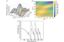
ObjectiveThe design and manufacturing technology of two-dimensional metrological planar gratings is complex and difficult. Design indicators and processing accuracy of two-dimensional (2D) gratings are important factors determining the performance of planar grating measurement systems. The grating type, grating pitch, groove depth, duty cycle, and characteristics of surface coating materials exert influence on diffraction efficiency and diffraction efficiency equilibrium. There are many parameter combinations and manufacturing methods for gratings. The development and process optimization of gratings feature long cycle time and low efficiency. Our purpose is to propose an accurate design and simulation method for two-dimensional planar gratings to provide sufficient accurate and fast support for grating development, shorten the cycle time of the design and processing of planar gratings, and improve development efficiency.MethodsThe design simulation of a silicon based two-dimensional planar grating is studied through the electromagnetic finite-difference time-domain (FDTD) method, and the simulation results are verified by experiments in this study. For two-dimensional grating structures, the FDTD algorithm only needs to simulate the smallest repeatable element with periodic boundary conditions. The calculation speed and accuracy meet the requirements and have been applied and verified in some grating simulations. By approximating and iterating the Maxwell equations in three-dimensional space, we can obtain the spatio-temporal changes in electromagnetic fields. One approximation method is called the central difference method. By linear interpolation approximation of physical quantities and selecting the appropriate truncation error level, high-precision approximation results can be obtained. The grating diffraction simulation in this study employs FDTD Solutions software and the grating unit in the simulation model consists of two parts, and the upper part is a columnar shape compatible with semiconductor technology. In this study, three structures are involved in sequence, including a regular prism, a ladder structure, and a ladder structure with rounded corners. The lower part is the substrate with the coating material of aluminum. Based on the input conditions of the different structure grating model, the actual process development and experimental verification are carried out. The incident light is a plane light pulse with a central wavelength of 780 nm, the incident angle is 27.9° with the normal direction onto the model, and the polarization directions P and S are calculated separately. The longitudinal boundary of the model is a perfect matching layer (PML) with a certain number of layers, and the incident light will pass through the boundary without reflection. The horizontal boundary is the Bloch boundary, which simulates the periodic arrangement of a single computing unit in the horizontal direction to obtain the grating structure. The mesh division of the simulation model is automatically achieved by software preset schemes, with dense grids near the aluminum bumps and loose grids in the air part. The mesh accuracy is generally adjusted between 2 to 4 nm based on convergence requirements.Results and DiscussionsFirstly, for the regular prism model, the measurement results of the diffraction efficiency of the first round grating sample are 12% for P-polarized light and 64% for S-polarized light. There are some differences between the simulated and experimental results. Combining the actual process results and grating test results, we try to optimize the model structure in the subsequent simulation and build grating simulation models of different structures and parameters, including the ladder structure grating and the ladder structure grating with rounded corner (Figs. 6 and 8). Secondly, the grating model with corner-rounded bump structure is close to the actual process results, and the final diffraction efficiency and polarization equilibrium meet the design requirements. The simulation results are consistent with the actual process results (Table 5). Thirdly, the FDTD simulation accuracy greatly depends on the simulation step size. The smaller step size leads to more accurate characterization of structural details in the simulation, whereas the larger requires computational amount results in longer calculation time. The simulation accuracy is also verified by reducing the simulation mesh size. The accuracy of mesh size 8 nm is acceptable (Table 3). Finally, at 170 mm×170 mm measurement range of grating, the diffraction efficiency, diffraction uniformity, and balance of P-polarized and S-polarized lights satisfy the grating design requirements (Fig. 14).ConclusionsWe study the design and simulation of two-dimensional planar gratings, put forward a simulation method, and conduct process experimental verification. Through the established FDTD simulation method, the variation of polarization diffraction efficiency of two-dimensional gratings under different structures and sizes is explored. The coating layer reflectivity, groove depth, and duty cycle are three main factors affecting the diffraction efficiency of the gratings. At a duty cycle from 45% to 46.7%, the diffraction efficiency of S-polarized light decreases with the increase of groove depth, while the diffraction efficiency of P-polarized light increases with the increase of groove depth. At a groove depth of 260 nm, the diffraction efficiency of different polarizations is nearly constant, and the diffraction efficiency and diffraction efficiency equilibrium meet the design requirements. The simulation results are close to the actual process results, and the simulation accuracy satisfies the requirements. Based on the established FDTD simulation method and manufacturing process, the design efficiency and process development efficiency of planar gratings can be greatly improved.
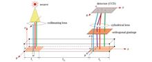
ObjectiveIn view of the contradiction between the high performance and small size in the micro-spectrometer, a two-dimensional (2D) dispersion system based on planar waveguide structures is proposed. With the increase in spectrometer application scenarios and the demand for device integration and light weight, the miniaturization of the spectrometer has become more demanding. Miniaturized spectrometers are divided into four main categories at present: dispersive optics, narrowband filters, Fourier transform, and reconstructive. However, most of them achieve better performance at the expense of the convenience of detection and the lightweight of the structure. At the same time, because of the restriction of the system size, there is an irreconcilable contradiction between high accuracy and wide wavelength range. To address the above problems, researchers have proposed solutions from the perspectives of increasing the wavelength measurement range and improving the wavelength resolution, respectively. But the conflict between high performance and small size still exists. The emergence of planar waveguides provides a new idea for miniaturized spectrometers. Therefore, the study on virtually imaged phase arrays (VIPA) appears, and it combines VIPA with the dispersion element to form a 2D dispersion expansion to improve the measurable wavelength and accuracy. However, the beam input conditions of VIPA are very strict, and the coating technology limits the increase in the measurable range of the wavelength. Therefore, we wish to propose a 2D dispersion system based on the lightweight of planar waveguides, with low input beam requirements and a measurable wide range of wavelengths.MethodsThe wavelength dispersion of the system includes two progress. First, the wavelength dispersion expands in one dimension. The collimated beam is transmitted inside the waveguide because of the diffraction of the coupled-in volume grating. The symmetric structure of the coupled-in and coupled-out volume gratings allows the beam to emit at the coupled-out volume grating, at an opposite and parallel angle to the input beam. Due to the dispersion of the volume grating, the diffraction angles of different wavelengths in the beam are different, which leads to different transmission periods in the waveguide. Finally, the positions of different wavelengths reaching the coupled-out volume grating are also different, so as to achieve a dispersion, namely, one-dimensional dispersion. In the process of analyzing the coupling position, it is found that different wavelengths may overlap at the same position periodically, which is the same as VIPA's output. Secondly, by adding an orthogonal grating after the waveguide system, the overlapping wavelength is subjected to secondary dispersion in another direction. Third, different wavelengths have different angles behind the cylindrical. Then the beam can focus on different positions of the detector, so as to achieve the one-to-one correspondence between the wavelength and the position. This is the whole process of the system to achieve 2D dispersion. The principle is simulated to verify its feasibility. At the same time, by combining the definition of free spectral range and the 2D dispersion diagram, the FSR and measurable wavelength range in the system are analyzed.Results and DiscussionsThe feasibility of the system in 2D dispersion is verified through theoretical analysis and software simulation. Theoretically, the corresponding relationship between wavelength and position on the detector is given. In the next part, the system is used to detect the wavelength of the monochromatic band (Fig. 9) and the visible light band (Fig. 10). It is found that the final dispersion results are related to the thickness of the waveguide and the length of the coupled-out volume grating. Therefore, the influence of these two factors on the 2D dispersion expansion is analyzed. Finally, it is found that a thinner waveguide and longer length of the coupled-out volume grating will lead to a wider measurable wavelength range. The wavelength measurable range of proposed system is improved compared with that of VIPA. For example, the existing spectrometer based on VIPA (such as hyperfine spectrometer) generally has a detection bandwidth of only about 50 nm, up to more than 100 nm, which cannot meet the needs of many applications. In comparison, the system proposed in this paper can reach more than 200 nm. In this way, the contradiction between the small size of the system and the wide wavelength range in miniature spectrometers is broken.ConclusionsThe 2D dispersion system based on planar waveguides proposed in this paper not only effectively utilizes the compactness of planar waveguides but also reduces the strict constraint on the input beam, and it improves the measurable range of wavelength. Meantime, combining its wavelength mapping after 2D dispersion with a high-pixel CCD array can further improve the wavelength resolution. The final analysis results show that the 2D dispersion system based on planar optical waveguides can measure a wavelength range of more than 200 nm, which is several times higher than that of the existing VIPA technology-based structure. Moreover, the system structure is relatively simple, and the technical requirements for the incident beam are not very strict. The system maximizes the use of the compact waveguide without increasing the component cost of the system and obtains better detection performance. The system provides a new idea for the development of miniaturized spectrometers.
ObjectiveGiven the lack of research on the complete design and optimization of multifocal intraocular lenses (IOLs), we propose the design process of diffractive multifocal IOLs focusing on the intermediate distance, and then analyze and optimize the effect of substrate parameters on diffraction efficiency. Multifocal IOLs are mostly based on the superposition of different diffractive optical elements (DOEs) design from inside to outside. When human eyes are in a bright environment, the pupil is relatively small and the edge diffraction periods may not be involved in imaging. Meanwhile, the imaging changes in the transition region and the light interference in adjacent focal points lead to deteriorated visual quality. Thus the multifocal design method with pupil size independent into the IOL optical design becomes a research hotspot, on which many scholars have conducted research. Additionally, as the common view distance of human eyes is intermediate in daily life, optimization of the intermediate distance in multifocal IOL design has also become the focus. On the other hand, DOEs in IOL systems are usually designed with large curvature substrates to carry more diopters due to design space limitations. Combined with the softer material, the diffractive structure is mostly tilted and inclined to be perpendicular to the large curvature substrates, and then the effect of the substrates cannot be ignored. With the continuously improving requirements for visual quality, the future design of IOL substrates will certainly be more inclined to aspheric substrate as a method to improve image quality. In this way, the analysis and optimization of the effect of aspheric substrate parameters on the diffraction performance can bridge the gap between theory and practice in ophthalmic lens design. Through theoretical modeling and simulation analysis, we put forward the analysis and solutions in the above two aspects and hope that our study could serve as a model for the design of diffractive ophthalmic lenses such as multifocal IOLs.MethodsOn one hand, for the diffractive multifocal IOL design, we analyze the multifocal diffraction efficiency model through diffraction phase changes based on the scalar diffraction theory. Then we build a design model of multifocal IOL based on the Liou-Brennan human eye model through optical software and simultaneously optimize the modulation transfer functions (MTFs) at near, intermediate, and far distances. Generally, the complete design process of diffractive multifocal IOLs is established through the study of diffraction efficiency and MTF optimization. On the other hand, for the case where the diffractive structure is often tilted and perpendicular to the substrates in IOL design, the schematic design of diffractive IOLs with aspheric substrates is established. By the relationship in the schematic, we derive the expression of period radius and actual phase delay for diffractive IOLs with aspheric substrates. Furthermore, the expression of the actual diffraction efficiency is given for our built multifocal phase profile model. For the example parameters of multifocal IOL design, we analyze and compare the differences between the actual diffraction efficiency and the theoretical diffraction efficiency in terms of the diopters and aspheric synthesis factors. Finally, an optimization method is proposed based on assigning corresponding weights to different periods to compensate for the effect on diffraction efficiency.Results and DiscussionsFirstly, the diffraction efficiency distribution of multifocal DOE is obtained by the theory model of phase profile [Eqs. (6) and (7)], and the relationship between phase delay β1, β2, and diffraction efficiency at each order and overall orders in our experiment is analyzed [Figs. 1(a) and 1(b)]. The diffraction phase profile is obtained according to the focused optimization design of intermediate distance [Fig. 1(c)], and the results show that the diffraction efficiency of the obtained model reaches 0.2685, 0.3597, and 0.2223 at far, intermediate, and near focal points, respectively (Table 1). A multifocal diffraction design focusing on intermediate distance optimization is also obtained. Meanwhile, we establish and optimize a diffractive multifocal IOL system by Zemax, and the MTFs of far, intermediate, and near distances are 0.5528, 0.5840, and 0.5570 at 100 lp/mm, respectively which exceed the MTF of the Liou-Brennan model at 100 lp/mm (Fig. 2) with high imaging quality of IOL design. Then the effect model of diffraction substrate parameters is proposed for the multifocal DOE phase profile design (Fig. 4), and the expressions of ophthalmic lens period radius, actual phase delay, and actual diffraction efficiency for aspheric substrates are obtained. Additionally, analysis of the actual diffraction efficiency can be employed to pick the substrate diopters and aspheric synthesis factors for ideal diffraction efficiency (Fig. 6). We further provide an optimization method, and the results indicate that the optimized diffraction efficiency is in close agreement with the theoretical value and achieves our optimization objective (Fig. 7).ConclusionsWe conduct the diffractive multifocal IOL design and substrate effect analysis. Firstly, the theoretical model of multifocal DOE design is analyzed, and a multifocal IOL focusing on intermediate distance is designed. The MTFs of the IOL at three focal points of far, intermediate, and near distance are 0.5528, 0.5840, and 0.5570 at 100 lp/mm, and the diffraction efficiency reaches 0.2685, 0.3597, and 0.2223, respectively. Then according to the phase profile of multifocal DOE, a theoretical model of the effect of diffractive substrate parameters on diffraction efficiency is built, and the theoretical model in terms of both substrate diopters and substrate aspheric synthesis factors is analyzed. Finally, we propose an optimization method for the substrate effect, and the optimization example shows that the optimization equation can reduce the influence on diffraction efficiency caused by substrate parameters. The design and optimization of multifocal IOLs with high imaging quality are realized, and the ideas can be applied in designing diffractive multifocal IOLs and other multifocal ophthalmic lenses.
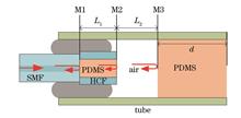
ObjectiveTemperature is the most basic and important physical quantity in scientific research and industrial production, so temperature measurement with high sensitivity is essential. Due to the advantages of corrosion resistance, high safety, electromagnetic interference resistance, small size, compact structure, and easy integration, the fiber optic Fabry-Pérot interferometer (FPI) sensor has widely drawn the attention of global scholars. However, the sensitivity of the all-fiber FPI temperature sensor is only 84.6 pm/℃ due to the low thermal expansion and thermal-optical coefficient of the quartz fiber. There are two effective ways to increase the sensitivity of FPIs. One is to use polydimethylsiloxane (PDMS) which has a high coefficient of thermal expansion, and the other is to generate vernier effect. The effective combination of PDMS and vernier effect will further improve the sensitivity of FPIs. In this study, a temperature sensor based on PDMS and vernier effect is proposed and fabricated. With the help of PDMS expansion and vernier effect, the sensor has excellent temperature characteristics.MethodsIn this study, a cascaded double-cavity temperature sensor based on PDMS sensitization is proposed, which is composed of a PDMS cavity and an air cavity in cascade (Fig. 1). The PDMS cavity is formed by filling PDMS into a section of hollow core fiber with one end fused with the single mode fiber (SMF). The air cavity is formed by filling the PDMS cavity into a tube with a section of PDMS. The optical paths of PDMS cavity and air cavity are close but not equal, so the vernier effect is generated, and an envelope appears in the spectrum. The two cavities have opposite temperature responses, so the sensitivity of the sensor can be greatly improved by vernier effect. When the temperature increases, the length of the air cavity changes greatly due to the expansion of the PDMS at both ends, which greatly improves the temperature response of the air cavity and results in a further increase in the sensitivity of the sensor. Under the dual action of PDMS and vernier effect, the sensor has excellent temperature characteristics.Results and DiscussionsThe temperature performance of the sensor are theoretically analyzed and simulated. In the simulation, the free spectral ranges (FSRs) of PDMS cavity and air cavity are 5.20 nm and 4.40 nm, respectively, and the obtained spectrum envelope of the cascaded structure is 32.20 nm (Fig. 2). When the temperature rises from 40 to 41 ℃, the PDMS cavity has a red shift of 0.9 nm, and the air cavity has a blue shift of 2.6 nm, while the spectral envelope has a blue shift of 24.8 nm, which is 27.6 times as much as that of single PDMS cavity and 9.5 times as much as that of the single air cavity. In the experiment, the sensor is put into a temperature control box, and its interference spectrum is measured by an optical spectrum analyzer (Fig. 6). There is an obvious envelope with the FSR of 32.9 nm in the interference spectrum of the sensor (Fig. 7), which shows that vernier effect is generated. When the temperature increases, the spectral envelope shifts gradually to a short wavelength (Fig. 7). The temperature rising and falling experiments are carried out to investigate the stability and repeatability of the sensor, and the peak wavelength of the envelope is recorded at every interval of 0.2 ℃. By linearly fitting the data of wavelength shift versus temperature in the range from 40 to 42 ℃, the sensitivities of -21.10, -20.25, -20.88, and -19.96 nm/℃ are obtained (Fig. 9), and the average sensitivity is calculated to be about -20.55 nm/℃, which is 37 times as much as that of a single PDMS cavity (0.56 nm/℃). The maximum error between the sensitivities is about 5%, and the error is mainly caused by the low resolution of the temperature control box. In addition, the sensitivity of the sensor is slightly lower than the simulation results (-24.8 nm/℃). The reason is that the PDMS in the sensor is not freely expanded, and its actual expansion is smaller than that in ideal conditions. Compared with other FPI sensors based on PDMS, the proposed sensor has the highest temperature sensitivity (Table 1).ConclusionsA cascaded double-cavity temperature sensor based on PDMS sensitization is proposed and prepared, which is composed of a PDMS cavity and an air cavity. The optical paths of the two cavities are similar but not equal, and the two cavities have opposite temperature responses, so the enhanced vernier effect is generated, and an envelope appears in the interference spectrum. In addition, the sensitivity of the sensor is further improved by the expansion of the PDMS at both ends of the air cavity. Under the dual effect of PDMS and enhanced vernier effect, the sensor has an ultra-high temperature sensitivity. The experimental results show that the temperature sensitivity of the sensor is about -20.55 nm/℃ in the range of 40-42 ℃, which is about 37 times as much as that of the single PDMS cavity. With the help of PDMS and vernier effect, the sensor has excellent temperature characteristics. Due to the advantages of electromagnetic immunity, compact structure, high sensitivity, excellent stability, and easy integration, the sensor is promising for applications in scientific research and industrial production.
ObjectiveSince the establishment of the information theory in 1948, most researchers have focused on narrowing the gap with Shannon-Hartley theorem. The traditional rectangular quadrature amplitude modulation (QAM) is widely used in optical communication. Although this modulation scheme is relatively mature, the rectangular modulation format is still far from reaching the Shannon-Hartley theorem. To bridge the difference between rectangular QAM and Shannon-Hartley theorem, researchers have developed constellation shaping techniques, namely geometric shaping (GS) and probabilistic shaping (PS). These techniques are based on power constraints and designed around conventional points, such as 16QAM, 32QAM, and 64QAM. In the case of a Gaussian channel environment, the probability distribution scheme of PS is based on Maxwell-Boltzmann distribution. In this case, it is combined with GS to form geometric PS; however, the geometric PS of conventional points corresponds to its appropriate transmission rate. For example, the 16QAM's geometric probability shaping is suitable for transmitting signals with an entropy of about 3, but it causes performance issues when it is below 3. Additionally, it does not offer any advantage in PS when the entropy of the transmitted signal is above 3. Thus, this article aims to study the geometric PS scheme of unconventional and continuous points. This scheme can flexibly adapt to the channel environment and transmit appropriate information entropy.MethodsIt is necessary to focus on the PS scheme for GS to design a geometric PS scheme under power constraints. The probability distribution can be obtained from the Maxwell–Boltzmann distribution. This article designs the most compact hexagonal layout scheme in a two-dimensional plane. The distribution of noise in Gaussian channels is uniform in all directions, and thus, the constellation points are considered circles that conform to the noise distribution in Gaussian channels. After selecting a compact layout scheme, power screening is carried out. In power-limited schemes, layout selection is carried out to maximize space utilization, and points with low power are selected for modulation. Matlab Gaussian noise function is used to simulate the noise in the channel; linear regions in the experimental equipment are used for the experiments. The experiments focus on verifying the relationship between entropy and constellation points, while the selection of optical wavelength, signal rate, and power is secondary. The receiver in the experiment adopts a machine learning approach that can greatly reduce the complexity of the reception aspect. Moreover, machine learning intersects with traditional hard decision methods and has almost the same error rate in Gaussian channels.Results and DiscussionsThis paper verified the coherent optical communication system with an information entropy of 3 and constellation points of 8-13, information entropy of 4 and constellation points of 16-23. The results show that, when the bit error rate is 5×10⁻³, the geometric PS under hexagonal arrangement has gains of about 1 dB and 1.3 dB compared with 8QAM and 16QAM, respectively. Additionally, the simulation and experimental verification of geometric shaping at 8 and 16 points show a performance improvement of about 0.1 dB and 0.22 dB, respectively, compared with rectangular QAM. The essence of constellation shaping is to exchange complexity for performance improvement. Before the advent of machine learning, the complexity improvement in reception was not proportional to the benefits and was thus not widely used. However, this article adopts machine learning methods for signal reception, and the curve results also meet the expectations.ConclusionsThe geometric PS scheme under the power limitation proposed in this article was validated via simulation and experiments. Our findings show that the proposed scheme can achieve better bit error rates under the same power and signal-to-noise ratio conditions as the traditional scheme. However, the shaping scheme slightly increases the complexity of the system and results in varying signal-to-noise ratio gains under different signal-to-noise ratio conditions. Note that this article shows only representative cases, and the results show that at least 1 dB of gain can be obtained from the perspective of bit error rate. Moreover, as number of constellation points increases, the benefits obtained from the perspective of bit error rate also increase. In the experimental part, machine learning is applied to constellation reception decisions. Consequently, the cost of constellation shaping is gradually becoming acceptable. As machine learning technology becomes more mature, there will be opportunities to apply it to constellation shaping in channel environments other than Gaussian channels.
ObjectiveAs one of the important properties of the light field, polarization plays an important role in the interaction between light and matter. The modulation of polarization plays an indispensable role in optical communication systems, fiber sensors, fiber lasers, and other fields. However, in view of the twist, defects, environment perturbations, and other factors in the process of optical fiber manufacturing, the manufactured optical fiber is not completely uniform, which introduces random birefringence and leads to unpredictable polarization states. Therefore, it is of great practical value to study optical fibers with excellent polarization states. Although the existing single-polarization single-mode negative-curvature hollow-core fiber has the advantages of simple structure, easy preparation, endless single-mode transmission, and low loss, due to the limitation of research habits and optical materials, the current research mainly focuses on common communication bands. But obviously, the mid-infrared band will become the next hot band of the negative-curvature hollow-core fiber. Research shows that a wavelength of 3-5 μm plays an important role in national defense, medical care, communications, and other fields, especially near the wavelength of 4 μm, which is an ideal band for quantum cascade detectors to detect low-level light. Single-mode single-polarization light helps to provide a more pure light source for quantum cascade detectors. Therefore, it is of great practical significance to study the single-mode single-polarization negative-curvature hollow-core fiber with a wavelength of 4 μm.MethodsA hollow-core anti-resonant fiber composed of six nested tubes working near 4 μm is designed, which can transmit single-mode single-polarization with low loss. The influence of structural parameters on fiber performance is calculated by using the control variable method. The capillary wall thickness will lead to an obvious change in the fiber loss with the working band, which is the key factor affecting the characteristics of the negative-curvature hollow-core anti-resonant fiber. Therefore, the capillary wall thickness is analyzed and optimized. Through the scanning study of the capillary wall thickness, the local optimal parameter values of the minimum fundamental mode loss and the maximum high-order mode extinction ratio in the 4 μm band are determined, and the design goal of the single-mode performance of the fiber is successfully realized. The second step is to optimize the capillary radius. This parameter mainly affects the polarization state of the fiber, and different parameter combinations of the six inner tube radii correspond to different implementation effects. The optimization of capillary radius successfully achieves single-polarization operation in a single-mode state. In the third step, the core diameter of the fiber is optimized. Although the study does not reflect the further optimization effect of the parameters that have been optimized and determined in the previous steps, the parameter design still retains the effective mode area and the maximum transmission power tolerance value of the fiber. The fourth step is to study and characterize the bending resistance of optical fiber. Research shows that this design fully meets the preset requirements for bending resistance and verifies that the natural advantages of negative-curvature hollow-core anti-resonant fibers, such as large effective mode field area and less substrate material coverage, can contribute to the bending resistance of the fiber.Results and DiscussionsA negative-curvature hollow-core fiber with low-loss single-mode single-polarization transmission is proposed and analyzed by the finite element method. By calculating the influence of fiber parameters on the fiber structure, the high-order mode extinction ratio reaches 163 (Fig. 3), and the fiber successfully realizes single-mode transmission. However, in order to further ensure the single polarization performance of the fiber, the size of the capillary radius is optimized, and the single polarization function is realized based on single-mode transmission (Fig. 4). In order to ensure that the fiber has good bending resistance, the critical bending radius of the fiber is defined, and it is found that the bending loss of the x-polarization fundamental mode of the fiber is always less than 10-3 dB/m (Fig. 7). In addition, the fiber structure also has a large effective mode field area (Fig. 8), which meets the transmission requirements of high power lasers. The results show that the designed structure achieves both single-polarization performance and single-mode transmission.ConclusionsIn this paper, a single-mode, single-polarization, low-loss, negative-curvature, hollow-core, and anti-resonant fiber is proposed. The substrate material of the fiber is As40S60, which is specially studied and experimentally prepared by Xi'an Institute of Optics and Precision Mechanics, Chinese Academy of Sciences. Its refractive index is 2.395 at 4 μm. It has low intrinsic loss and great chemical stability in the mid-infrared band, which is beneficial to realize the low loss performance of the fiber. The fiber structure adopts a six-nested, capillary-type, negative-curvature, hollow-core, and anti-resonant structure with relatively mature preparation technologies and a simple structure. After optimizing the parameters of the fiber, the single-mode single-polarization effect can be achieved from 3.99 μm to 4.00 μm. Especially at the wavelength of 4 μm, the polarization extinction ratio (PER) and high order mode extinction ratio (HOMER) reach 491 and 694, respectively, which meet the conditions of single-polarization single-mode transmission, and the loss is as low as 1.8×10⁻⁴ dB/m. The fiber also has excellent bending resistance. At the wavelength of 4 μm, single-mode single-polarization transmission of the fiber can be achieved by selecting the appropriate bending radius at any bending angle. When the bending angle is equal to 0°, and the bending radius is from 1 cm to 10 cm, the confinement loss of the fiber is less than 5.3×10⁻³ dB/m. The negative-curvature, hollow-core, and anti-resonant fiber proposed in this paper has the advantages of simple structure, single-mode single-polarization operation, low loss, and excellent bending resistance. It can not only be applied to the communication industry and medical system but also is expected to provide a more pure light source for quantum cascade detectors operating in the band of 4 μm.
ObjectiveOptical orthogonal frequency division multiplexing (OOFDM) technology features the advantages of high spectral efficiency and strong anti-dispersion ability and is of immense interest in optical communication. Additionally, based on the different detection methods at the receiver, optical communication systems are divided into direct detection (DD) and coherent detection systems. Compared with the coherent detection system, DD-OOFDM system has the advantages of low cost, simple structure, and insensitivity to spectral offset and phase noise. Therefore, DD-OOFDM optical communication systems have been widely used. The realization of high-speed information transmission in the DD-OOFDM communication systems ensures convenience; nonetheless, information security issues are emerging, such as illegal personnel stealing information through fiber bending and other means; therefore, securing optical communication has become crucial. Compared with traditional encryption methods, chaotic encryption is advantageous because of its hard-to-predict nature and limitless chaotic sequence values. Using chaotic mapping sequences to derive keys with no regularity can improve the security of the system. However, in a DD-OOFDM communication system supporting chaotic encryption, since the receiver needs to receive sufficient encrypted information to decrypt it correctly, higher requirements are posed on the system BER. The presence of OOFDM subcarrier beat interference (signal to signal beat interference, SSBI) at the receiver end of the DD-OOFDM system significantly increases the system BER; thus, reducing SSBI becomes the key to improving transmission performance. The traditional method is to insert a protection interval to avoid the overlap of SSBI and OFDM signals, thus eliminating SSBI. However, this decreases the spectrum utilization of the system. The Kramers-Kronig (KK) receiver has the advantages of high spectrum utilization, low hardware complexity, and simple implementation, which can solve the aforementioned problem efficiently. For this reason, the use of a KK receiver at the receiver side is recommended to eliminate SSBI.MethodsIn this study, image transmission is considered as an example; at the transmitter side, the image pixel values (range 0-255) are first converted into 8-bit binary numbers, subsequently into a string of binary bit streams, and finally scrambled into random binary bitstreams. Thereafter, a double chaotic sequence is used to encrypt the bitstreams, with two chaotic sequences set to initial values of 0.2 and 0.7, respectively, and set μ to 4.0. The first or second chaotic sequence is used for encryption based on if the corresponding pixel location is odd or even, respectively. In the encryption process, since the chaotic mapping sequence generates values distributed in the interval [0, 1], if left untreated, they will directly become 0 or 1 in MATLAB software, thereby causing the encryption accuracy to decrease and number of iterations of the chaotic sequence to increase. Therefore, in this study, each chaotic value generated is multiplied by a larger number, such as 1015, and subsequently, this chaotic value is remaindered against 256 to ensure that it is an 8-bit binary number when it is heterogeneous with the pixel value. This allows a chaotic value to be processed with a corresponding pixel value, lowering number of iterations of the chaotic encryption algorithm. Subsequently, the encrypted data are combined with OFDM modulation for optical modulation. This study proposes eliminating the SSBI existing in the receiver side of the DD-OOFDM system using the KK receiver to reduce the BER and improve the system transmission reliability on the basis of secure transmission. Specifically, this study analyzes the structure of the KK receiver and the condition of its function that the input signal is the minimum phase signal, and simulates and tests the BER of the DD-OOFDM system based on the KK receiver.Results and DiscussionsAt the transmitter side, this study uses two chaotic sequences for data encryption, where the initial value x0 of the logistic chaotic mapping changes only by 10-6 orders of magnitude, and less than 100 iterations are need to produce completely different chaotic sequences (Fig. 5). Theoretically, the initial value x0, control parameters μ, and number of iterations n all affect the key space. For example, in double chaotic sequence encryption, the data x0 has 32 bits, and the nature of chaos enables the generation of a completely different chaotic sequence even at one bit deviation in x0; thus, the key space is approximately 264. Combining the above factors, the overall key space of the system can reach approximately 2192, which effectively prevents brute force cracking. Most of the image pixel point values before encryption are concentrated around 250, an extremely uneven distribution, demonstrating the correlation between pixel points to a certain extent, is easy to be cracked by the eavesdropper and hence is less secure. The scrambled and encrypted image and pixel values are completely different compared with the original image, and the pixel values of the encrypted image are uniformly distributed between [0, 255], which destroys the correlation of pixel values in the original image with high security, rendering it difficult for an eavesdropper to launch the original image from it (Fig. 11). At the receiver side, when the CSPR is sufficiently large to cause the KK receiver to meet the minimum phase condition, it can eliminate the SSBI and reduce the BER (Fig. 12). The image after chaotic decryption using the KK receiver is essentially the same as the original image, with only a few noise points (Fig. 13).ConclusionsTo achieve a safe and reliable data transmission in DD-OOFDM systems, this study conducted specific analysis, design, and implementation. To solve the security problem in DD-OOFDM systems, chaotic encryption is proposed. Chaotic mapping has the characteristics of randomness and limit nonconvergence, rendering the key space extremely large and thereby improving the encryption security. The original data are processed by double chaotic sequence encryption at the transmitting end of the system to reduce the correlation between the data substantially and ensure data security. To improve the spectral efficiency of the system, OFDM is used to modulate the encrypted data at the transmitter side of the system. At the receiver side, the SSBI in the signal after direct detection is processed, and a KK receiver is proposed to solve this interference. The structure of the KK receiver and the minimum phase signal conditions that render it successful are analyzed at the receiver side. Thereafter, the optical carrier power is changed by controlling the DC bias voltage of the laser driver so that the signal input to the KK receiver meets the minimum phase. With a CSPR of 11 dB, the system performs efficiently, with the KK receiver below the forward error correction threshold of the unutilized KK receiver.
ObjectiveThreat event recognition is one of the widely researched topics in distributed fiber optic sensing. Deep learning is an important means for pattern recognition. The main challenges that limit its recognition accuracy can be categorized into two aspects: lack of generalization and existence of false recognition for some signals with low vibration intensity and obscure features. On one hand, this is due to ambiguous features, such that the target signal is often obscured in noise, and on the other hand, such signals are easily mislabeled in the process of constructing data sets. The classification accuracy of neural networks can be improved in three ways. The first approach is to preprocess the data from the front end of the network by applying various methods, such as band-pass filtering, wavelet denoising, and Hilbert transform. However, these methods have relatively limited positive effects and will contribute to the loss of detailed information to some extent. The second approach is to increase the extraction of features from training samples, such as inputting multiple features of the signal into the network simultaneously to improve the recognition accuracy through feature fusion. The third approach is to increase the means of feature extraction through various methodologies, such as increasing the number of convolutional layers, introducing recurrent neural networks (RNNs), and supplementing deep belief networks. The design of specific schemes should consider the data characteristics of the sensing system. In this study, the sampling rate and sampling points of the Mach-Zehnder interferometer (MZI) are 50 times greater than those of the phase-sensitive optical time-domain reflectometer. Thus, the third approach will substantially increase the computations and response time. In this paper, we attempted to implement the enhancement of vibration features from the perspective of signal sources for improving the recognition accuracy of weak vibration events under the traditional network framework.MethodsThe proposed recognition program employs the conventional waveform, frequency spectrum, and time-frequency spectrum feature extraction method; further, RNNs are not introduced in this method to avoid excessive computations. We optimized the conventional recognition strategy from the perspective of sample sources. We used empirical mode decomposition (EMD) to decompose the signal into multiple intrinsic mode functions (IMFs). The target signal exhibits clearer vibration features on certain IMFs. Specifically, the vibration part shows sharp pulses separated from the fundamental noise that exhibit higher contrast than the response pulses at the same location of the original waveform (Fig. 4). Furthermore, the frequency spectrum of the IMF shows distinct morphological features with suitable same-class consistency and inter-class differentiation (Fig. 5). These features are independent of the signal strength, which provides a feasible premise for the effective identification of weak vibration events. Based on the statistics of a large number of samples, IMF2 and IMF3 are selected to extract their waveform features and time–frequency spectrum features and forIMF2-IMF5 to extract their frequency features. The neural network consists of convolutional operators and fully connected networks. The waveform and frequency features are extracted using one-dimensional convolutional operators, while the time-spectrum features are extracted using two-dimensional convolutional operators (Fig. 6). In addition, based on the same feature extraction framework, four control groups were designed with the original signal as the sample source (Table 1).Results and DiscussionsBy comparing val_accuracy, val_precision, val_recall, and other parameters (Fig. 8, Fig. 9, Table 2, Table 3, Table 4, and Table 5), the proposed model was found to be the best in terms of recognition accuracy, stability, and generalization. Although all the models exhibited high accuracy when using the training set, the metrics in the test and validation sets showed a significant decrease compared with the training set. Only the validation accuracy of Model 1 (our strategy) exceeded 90%, which remained relatively stable. The classification accuracy of the model for specific events can be characterized using precision, recall, and F1_score; all three parameters are greater than 90% in Model 1. The average response time of the proposed model is less than 0.07 s, indicating good feasibility and development space.ConclusionsIn this paper, we have proposed a classifier Model 1 based on EMD and convolution operators using the Mach–Zehnder interferometer (MZI) as the sensing system. Instead of the original signal, IMF2 and IMF3 were selected to extract contour features and time–frequency domain features, and IMF2-IMF5 were selected to extract the frequency spectral features. Four control groups were developed based on the same feature extraction framework with the original signal as input. The test_accuracy and val_accuracy of Model 1 are 97.02% and 94.88%, respectively, while the val_accuracy of the remaining control groups is less than 90%. The average val_precision and val_recall of Model 1 for the five vibration events are 95.51% and 94.42%, respectively. In particular, for two weak vibrations, Event 4 and Event 6, the recognition accuracy of Model 1 exceeded those of other control groups, thereby fully demonstrating the optimization of this scheme in terms of generalization and vibration recognition. This paper improves the conventional deep learning network from the perspective of sample sources; however, it does not change the conventional feature extraction, and further extension of the feature extraction dimension is required in the subsequent development stage to address the shortcomings of the existing classifier. In addition, the selection of IMF components in this study is based on the target signal features and the statistical results of large batch samples, and the selection in practical applications need not be limited to this paper.
ObjectiveRefractive index (RI) is one of the most important parameters to guide light and control light-matter interaction. Recently optical fiber RI sensors have attracted great attention in various areas such as physics, photonics, chemistry, biology, and environment monitoring due to their remote on-line sensing. The optical Vernier effect produced by the cascade of two interferometers with close free spectral ranges (FSRs) has been developed to improve the sensitivity of RI sensors. The wavelength shift of the spectral envelope of the cascaded sensors is much larger than that of the unit sensing interferometer when the environmental refractive index is changed. FSRs of the two unit interferometers, determined by the interferometer's cavity lengths, should be carefully designed and calibrated to improve sensitization fold as much as possible. Additionally, both of the two unit interferometers should have high fringe visibility and stable interference components for obtaining obvious cascaded spectral envelopes. Till now, the most reported unit interferometer for Vernier sensitization is the Fabry-Perot interferometer (FPI). Unfortunately, the fabrication of an FPI interferometer requires complicated fiber alignment and fine cavity length adjustment, which leads to poor reproducibility in the sensor fabrication. Michelson interferometer (MI) can also be employed as a unit interferometer for Vernier sensitization. Those traditional MI unit interferometers usually include multi-mode fiber, twin core fiber, and coreless fiber. In the aforementioned fibers, multiple cladding modes are inevitably stimulated and multiple modal interference are involved in the spectrum of the cascaded sensor. As a result, interference component analysis of the spectrum is complex. In addition, controllable stimulation of these modes is difficult. Few-mode fiber (FMF) could only support the transmission of limited modes. The decreased mode quantity leads to a simple interference component, which is beneficial to the sensor cascade. The interference component in an FMF-based MI is stable since all the modes in FMF are confined in the fiber core and immune to environmental refractive index changes. Meanwhile, MI could be naturally formed by the two end faces of a single FMF, without the necessity for fiber alignment and fine cavity length adjustment. Thus, FMF-based MI is a good candidate for reference interferometers in Vernier sensors. In this study, an FMF-based MI-FPI Vernier sensor has been developed for RI sensitization. FPI acts as a sensing interferometer because of its open cavity, and MI made from an FMF serves as the reference interferometer due to its simple interference component and stable interference spectrum. Due to FMF and MI, the dual cavity mismatching problem and poor controllability of traditional dual FPI sensors could be solved.MethodsFor the proposed FMF-based MI-FPI sensor, MI is implemented by fusing an incident single-mode fiber (SMF) with an FMF in a certain core-offset, and FPI is formed by the cavity sandwiched between the free end face of the FMF and one of the end face of an another SMF. Both FMF and the two SMFs are fixed on a slide by UV glue. The interference spectrum of the FMF-based MI is mainly affected by two structural parameters including the offset between incident SMF and FMF, and the FMF length. Offset fusion will induce asymmetrical optical mode field distribution in fiber and excite the specific mode. Thus, the influence of core-offset distance between SMF and FMF on mode excitation efficiency, and the effect of FMF length on the Vernier sensitization effect are simulated. Moreover, a virtual MI is developed to analyze the Vernier enhancement effect on unit FPI to provide theoretical guidance for the FMF length selection. The interference component in the cascaded structure is analyzed by taking a fast Fourier transform (FFT) of the experimental spectrum. Due to FFT, the spatial frequency of a certain interference component can be ascertained, and based on simulation data the cascaded MI-FPI sensor is fabricated. The sensor fabrication is as follows. Firstly, an FMF-based MI with the FMF length of 32.4 cm and the core-offset of 3 μm is fabricated. Then, an FPI is formed by gradually drifting another SMF to the end face of the FMF. Both FMF and the two SMFs are fixed on a slide by UV glue. The interference spectrum of the fabricated MI-FPI sensor is recorded by an optical spectrum analyzer (YOKOGAWA, AQ6370) with a resolution of 0.02 nm. A super-luminescent light-emitting diode (SLED) with a wavelength range from 1500-1600 nm is adopted as the light resource. For RI measurement, NaCl solutions with different RI in a range of 1.3384-1.3412 are employed and the RI of each NaCl solution is determined by an Abbe refractometer.Results and DiscussionsRefractive index response sensitivity of the cascaded MI-FPI sensor is measured to be 12466.956 nm/RIU in the range of 1.3384-1.3412, which is 12.29 times enhanced over the FPI sensor without MI cascade. The amplification limit and the influence factors are analyzed, and the sensitization limit of the sensor is determined by the ratio of ξS/ξR-ξS. Thus the sensor sensitivity could be further improved in the following two ways. One is to adopt a light source with a wider spectrum to decrease ξR-ξS, and the other is to raise the FPI cavity to increase ξS. The experimentally measured magnification factor slightly deviates from the theoretical one. The possible reasons are discussed. Firstly, followed by inverse Fourier transform, a frequency filtering method is utilized, which is suitable for analyzing cosine signals. However, since the spectrum of the experimental MI is not a regular cosine spectrum, the FSR at short wavelengths is smaller than that at long wavelengths, leading to a deviation between the experimentally measured magnification factor and the theoretical one. Secondly, during the experiment, there are small errors in the length control of FMF and FPI, which is the cavity length of MI (LR) and FPI (LS), also resulting in certain deviation of the magnification factor.ConclusionsA refractive index Vernier sensor based on an FMF-MI is developed. The sensor consists of an MI serving as the reference unit interferometer and an FPI serving as the sensing unit interferometer. Experimental results show that the MI-FPI sensor has a refractive index sensitivity of 12466.956 nm/RIU in the range of 1.3384-1.3412, which is 12.29 times improved compared with the FPI sensor without MI cascade. The proposed MI-FPI sensor is characterized by high sensitivity, simple fabrication, and sound reproducibility. Therefore, it can be a suitable choice for various applications in biological and chemical fields. Furthermore, the FMF-based MI has the unique advantages of simple structure, high extinction ratio, excellent stability, and mode controllability, which is suitable to be employed as a reference interferometer cascaded with other interferometers to achieve the Vernier effect.
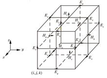
ObjectiveIn response to the need for high-precision and engineering applications of resonant fiber optical gyroscopes (RFOGs), research is conducted on the relevant factors that affect polarization noises and thus the output error of gyroscopes in varying temperature environments. Polarization noise is one of the main optical noises that cause output errors in RFOGs. Since the core sensitive component of RFOGs, namely the fiber ring resonator (FRR), is mostly wound by polarization maintaining optical fiber, when the birefringence index of polarization maintaining optical fibers changes with temperature, it will cause the superposition and interference effects of the resonant light waves corresponding to the two intrinsic polarization states of the resonator, resulting in asymmetry in the resonance curve, polarization noises, and detection errors at the resonance frequency point and thereby causing gyro output errors. Therefore, suppressing polarization noise in varying temperature environments has profound significance. The measures taken by researchers to suppress polarization noise can be divided into two categories: stabilizing the phase difference between primary and secondary polarization and reducing the intensity of secondary polarization states. Researchers have successively adopted a single 90° fusion joint scheme within the FRR, a twin 90° fusion polarization maintaining transmission FRR scheme, and a secondary polarization axis rotation fusion polarization starting resonant cavity to stabilize the primary and secondary polarization phase difference. Researchers have reduced the intensity of secondary polarization states by inserting polarization controllers, online polarizers, etc. into the FRR or utilized a new fiber optic scheme to reduce the impact of polarization noises on the gyroscope. The above studies have achieved good results in noise suppression, but most studies have been conducted at room temperature or small-range temperature variations. When facing engineering applications, gyroscopes need to improve their environmental adaptability within the full temperature range. To meet the needs of both high-precision and engineering applications, we study the factors that affect polarization noises and thus the output error of gyroscopes in varying temperature environments.MethodsJones matrix is a relatively simple method to describe the polarization characteristics of optical devices. We establish a complete optical transmission model based on the Jones matrix method. By analyzing the clockwise and counterclockwise optical transmission in the resonant cavity, the difference between the coupling errors of the clockwise and counterclockwise polarization modes is used as the output error of the gyroscope, eliminating the common mode error, and the problem of using double the frequency deviation caused by polarization noise as the output error of the gyroscope in the past while ignoring the difference in forward and backward light transmission is solved. In the full temperature range of -40 ℃-80 ℃, the factors that affect the polarization noise and lead to the gyro output error are simulated and calculated, including the angle alignment error of the coupler, the length difference of the optical fibers on both sides of the twin 90° fusion point, and the uneven temperature distribution difference of a section of optical fibers on the FRR or each adjacent end of optical fibers when the system is locally heated, so as to obtain the gap between the actual structure of the system and the theoretical calculation and quantify the control accuracy of relevant parameters based on specific gyro error requirements in varying temperature environments.Results and DiscussionsFirst, based on the twin 90° fusion point integrated online polarizer structure, the resonant cavity optical path is modeled, and its polarization characteristics are analyzed to obtain the resonance curves of the clockwise and counterclockwise light transmission in the cavity for one cycle (Fig. 2). In addition, the frequency difference between clockwise and counterclockwise is taken as the output error of the gyroscope caused by polarization noises, and the influence of polarization errors on the gyroscope output under varying temperature environments is studied. When the ambient temperature changes within the whole temperature range, the errors caused by the polarization of clockwise and counterclockwise light transmission are very close, both within ±3 (°)/h, and the overall difference is within ±0.02 (°)/h, both showing periodic changes with temperatures (Fig. 3). However, this result cannot support the development requirements of the navigation level gyroscope engineering prototypes, and parameter control is needed to reduce the polarization error output. The relationship between the angle alignment error of the coupler (Fig. 4), the fiber length difference on both sides of the twin 90° fusion point (Fig. 5), and the output error of the gyroscope is simulated and calculated. Based on the control parameters obtained from this result and the gyro operating environment, active devices such as lasers or circuit components dissipate heat during normal operation, resulting in local temperature disturbance to the FRR close to them (Fig. 6), and the influence of the fiber ring temperature and its ambient temperature distribution difference on the gyro output error caused by polarization noise is analyzed, including the non-uniform temperature distribution difference on a section of optical fiber (Fig. 7) and the temperature distribution difference between two adjacent optical fibers (Fig. 8), which guides error distribution design due to polarization noise in varying temperature environments.ConclusionsWe establish a complete optical transmission model for FRR based on the Jones matrix. By analyzing the polarization noise of the clockwise and counterclockwise optical transmission and adopting the dual point 90° fusion integrated online polarizer structure, the resonance curve in FRR is derived, and the gyroscope output caused by polarization error in varying temperature environments is obtained; due to the periodicity and regularity of the gyroscope output within the whole temperature range, the varying temperature range of -40 ℃--20 ℃ is used instead of the full temperature environment, and different influencing factors are analyzed separately. The results show that when the extinction ratio of the online polarizer is 30 dB, the alignment error of the coupler angle is less than 2.78°, and the output error of the gyroscope is less than 0.01 (°)/h; as the coupler coefficient k gets larger, the fault tolerance value of the fiber length difference on both sides of the double 90° fusion point becomes higher. When k is 0.05, and ΔL is controlled within 0.207 m, there is a gyroscope output error of less than 0.01 (°)/h. On this basis, when the temperature distribution on a section of optical fiber is uneven due to the internal temperature rise of the gyro prototype in engineering applications, the difference of the uneven temperature distribution should be less than 13.2 ℃; when there is a non-uniform temperature difference between every two adjacent fibers on the FRR, its value should be less than 3.122 ℃, and the output error of the gyroscope is less than 0.01 (°)/h. The above analysis is based on the requirements of suppressing polarization noises in gyroscopes, which provides certain theoretical guidance for error allocation design in full-temperature environments.
ObjectiveTo solve the problems of narrow linear dynamic range and weak anti-interference ability of the Pound-Drever-Hall (PDH) technique, a PDH frequency stabilization method based on two modulation depths and two error signals is proposed herein. The PDH technique is widely used in the fields of laser frequency or optical resonant cavity locking. The traditional PDH technique usually utilizes a modulation depth of 1.08 rad to obtain the most sensitive error signal. However, the traditional PDH technique, used for frequency stabilization, is susceptible to environmental disturbances and loss of lock owing to the narrow linear dynamic range of error signals. In addition, only when the phase of a local demodulation signal matches the phase of an interference signal reflected by the cavity, the error signal with the highest sensitivity can be obtained. Currently, most methods manually adjust the initial phase of the local demodulation signal to achieve phase matching; these methods exhibit low accuracy and cannot realize automatic locking easily. Therefore, an adaptive locking mechanism having large modulation depth with large linear dynamic range error signal and small modulation depth with high-sensitivity error signal is developed to achieve frequency stabilization with strong anti-interference ability and high precision.MethodsFirst, a digital quadrature demodulation technique was used to accurately extract the phase of the interference signal to achieve automatic matching between the phases of the local demodulation and interference signals. Second, a new error signal (Spre) was realized using the transmitted power signal Ptran and traditional error signal SPDH to enlarge the linear dynamic range of the PDH frequency stabilization system. Then, Spre corresponding to the large modulation depth was used to realize fast capture and prelocking. Finally, SPDH corresponding to the small modulation depth was used to realize precise locking. After locking, the modulation depths and error signals could be automatically switched according to the amplitude change in Ptran, realizing frequency stabilization with a large linear dynamic range and high sensitivity in the PDH technique. A frequency stabilization control system based on a field-programmable logic gate array (FPGA) was developed, and a locking test was conducted on a Fabry-Perot cavity. The experimental results show that the adaptive locking mechanism with double modulation depths and double error signals can greatly improve the anti-interference ability of the locking system with precision locking.Results and DiscussionsConsidering the influence of phase mismatch and narrow linear dynamic range on the frequency stabilization accuracy of the PDH technique, an adaptive frequency stabilization method with a large linear dynamic range based on two modulation depths and two error signals is proposed herein. The phase of the interference signal is obtained using the digital quadrature demodulation technique to realize phase matching between the interference and local demodulation signals to improve the sensitivity of the error signal SPDH obtained using the PDH technique (Fig. 3). To improve the anti-interference ability of the locking system, Spre with a large linear dynamic range is constructed and combined with SPDH and Ptran (Fig. 4). The adaptive locking mechanism using large modulation depth to obtain Spre and small modulation depth to obtain SPDH is designed herein (Figs. 5 and 6). Thus, the proposed locking mechanism has the highest sensitivity and linear dynamic range, affording high precision and strong anti-interference locking. A locking control system based on FPGA was designed herein (Fig. 7), and a locking test was conducted on the Fabry-Perot cavity. The test results show that the linear dynamic range of Spre corresponding to β= 1.80 rad can reach 6.04 nm (Fig. 8), which is ~3.4 times that of SPDH corresponding to β= 1.08 rad. The automatic switching and locking mechanism based on two modulation depths and two error signals can realize relocking of the Fabry-Perot cavity after instantaneous detuning (Figs. 10 and 11). The long-term relative stability of the Fabry-Perot cavity is 5.72×10⁻⁹ (Fig. 12). Therefore, the proposed adaptive PDH frequency stabilization method can achieve long-term precise locking of the optical cavity/laser frequency.ConclusionsThis study proposes an adaptive frequency stabilization mechanism using two modulation depths and two error signals to modify the traditional PDH technique to achieve large linear dynamic range, high locking accuracy, and strong anti-interference ability. The test results show that the linear dynamic range of Spre corresponding to a large modulation depth of 1.80 rad can reach 6.04 nm, which is ~3.4 times that of SPDH (1.78 nm) corresponding to a small modulation depth of 1.08 rad. The adaptive switching and locking mechanism using two modulation depths and two error signals can substantially improve the anti-interference ability of the locking system, with precision locking. The relative stability of the locked cavity reaches 5.72×10⁻⁹ within 3 h. Thus, the proposed method can be widely used in fields such as laser frequency locking and resonant cavity locking.
ObjectiveWith the continuous development of spatial light modulators, it has been widely applied in many fields, such as light field control, beam shaping, beam deflection, and holographic reproduction, with unparalleled advantages. However, due to limitations of process conditions, it also has many defects. The existence of zero-order spots and multi-order diffraction images caused by its own "black-matrix effect" will exert certain effects on the quality of the output light field, which leads to a low utilization rate of light energy and poor uniformity of reproduced images. However, most studies nowadays are conducted from the perspective of algorithm design to improve the reproduced image quality of holographic display. But when the liquid crystal spatial light modulator (LC-SLM) is employed for holographic display, due to the influence of the "black-matrix effect", the light energy distribution of the reproduced results follows the sinc function distribution, so that the energy distribution of the reproduced images is not uniform. We propose a method to improve the uniformity of the reproduced images through digital blazed grating to deviate the reproduced images and combine with the phase compensation method of the holographic reproduction domain model. This method provides theoretical assistance to improve the quality of reproduction results when LC-SLMs are leveraged for holographic reproduction.MethodsBased on the principle of Fresnel hologram calculation, our main design principle is analyzing the influence of zero-order spots and multi-order diffraction images produced by the "black-matrix effect" of the LC-SLM adopted for holographic reproduction on the results. Then with an aim at avoiding the offset of the zero-order spots on the reproduced images by digital blazed grating superimposed on the hologram, and finally to compensate for the uneven distribution of light energy, the phase is compensated according to the proposed reproduction domain model. The steps are as follows. First, the reproduction domain is determined according to the size of the reproduction image, and after loading a certain period of digital blazed grating based on the original design hologram, the compensation amount is inverted according to the light intensity distribution of the reproduction domain reproduction results and then synthesized with the original light wave. Recalculating the hologram can achieve the adjustment of the reproduction results. The quality of the holographic reproduction results is improved by avoiding the influence of zero-order spots on the reproduction results.Results and DiscussionsDue to the influence of the grid structure when LC-SLM performs holographic reproduction (Fig. 2), when the hologram is loaded, the reproduction results shown in Fig. 4 will have multi-order diffraction images and zero-order spots, which seriously affects the quality of the reproduction results. We propose the phase compensation method of the reproduction domain model (Fig. 6) according to the digital blazed grating deviation from the reproduction image and then compensate the phase according to the light energy of the reproduction domain, which can improve the uniformity of reproduction results. the calculation flow chart is shown in Fig. 8(b). Through the optimization calculation and simulation verification of the phase compensation amount and the construction of the holographic reproduction optical path (Fig. 14), the phase after compensation calculation is loaded onto the SLM for reproduction experimental verification and tests. The experimental results show that the uniformity of the reproduced image after compensation is twice as much as that of the original one, and the utilization rate of light energy is also improved to a certain extent, as shown in Figs. 16 and 17.ConclusionsWe analyze the light energy distribution of the reproduced image when the LC-SLM performs holographic reproduction, and propose a phase compensation method through the reproduction domain model to compensate for its phase. The results show that after adding a certain period of digital blazed grating to the design hologram, the compensation amount is inverted according to the distribution of light energy in the reproduction domain, and then synthesized with the original light wave and redesigned to calculate the hologram. The uniformity of the reproduced results is twice as much as that of the unimproved one, and the utilization rate of light energy is also improved. The experimental results prove that the method can effectively improve the uniformity and light energy utilization of holographic reproduction results while avoiding the effect of zero-order spots when LC-SLMs are employed for holographic reproduction. The results of this study are useful for improving the quality of output results when spatial light modulators are adopted for light field modulation and holographic reproduction.
ObjectiveThe foveated imaging simulates the characteristics of human eye imaging, which can achieve global imaging of detection targets with a large field of view and realize local high-resolution imaging for target detail discrimination. This technology has been applied to the large field of view imaging such as scene monitoring, danger detection, remote sensing, and target tracking, so as to reduce the complexity of bandwidth and optical systems. The strategies for implementing foveated imaging in the past include non-uniform sensors with variable photosensitive density for imitating the variable sampling rate of the retina, designs of foveated optical systems, calculation integration of independent imagers with different resolutions, and a single sensor with multiple channels segmented into different magnification ratios. However, the high cost of hardware, the complexity added by non-uniform sensors, and the complexity of foveated optical systems, usually make these solutions unattractive. We propose a dynamic foveated optical imaging system consisting of an object-side telecentric lens, a liquid crystal lens with a rectangular aperture, an optical sensor, and a polarizing film. The object-side telecentric lens reduces the effect of oblique incident light on the imaging of the liquid crystal lens by making the main image ray in the object plane parallel to the optical axis. By introducing a liquid crystal lens with a rectangular aperture to modulate the phase of light waves, the system achieves local high-resolution imaging, and the center of the lens can be moved in real time according to actual situations. In other words, while ensuring high-resolution imaging of the target of interest in real-time detection, the entire image plane can be scanned, and other areas have low-resolution imaging. The lightweight and small volume of the liquid crystal lens with a rectangular aperture makes the entire optical system more compact.MethodsThe same liquid crystal material (HTW137700-100, Jiangsu Hecheng Co. Ltd.) in Fig. 4 is used to fabricate a liquid crystal lens with a rectangular aperture, with a clear aperture of 5 mm×5 mm according to the structure in Fig. 1. The high impedance film material of the lens is aluminum-doped zinc oxide with a resistance of 3×10⁶ Ω/□, and the thickness of the liquid crystal cell is 30 μm. The interference fringes of the liquid crystal lens under the driving conditions in Table 1 are measured by using Mach-Zehnder interferometry (Fig. 3). It can be seen that the actual aperture of the liquid crystal lens is smaller than the clear aperture, and the position of the lens varies with the driving voltage. The ordinary refractive index of the nematic liquid crystal used in Fig. 4 is 1.513, and the extraordinary refractive index is 1.774. With a laser of wavelength 532 nm, the bright/dark changes of the liquid crystal cell with voltage are observed, and the phase delay of the liquid crystal is obtained as a function of the effective voltage. It can be seen that within the linear response range of the liquid crystal, which is between 0.6 V and 1.52 V, the phase delay is approximately linearly related to the effective voltage. When the voltage is higher than 1.52 V, the response curve is in the nonlinear region, and when the voltage is higher than 2 V, the liquid crystal tends to be saturated. Therefore, according to Eqs. (5) and (6) and the electric field simulation results in Fig. 2, the actual aperture of the liquid crystal lens is determined to be a circular area with a diameter of 1.56 mm centered at the origin of the liquid crystal lens in Fig. 3. By analyzing the effective area of the liquid crystal lens in Fig. 3, the focal length at different positions of the lens center is determined to be 8.2D, and the aberration is (0.1±0.02)λ. The wavefront map of the lens is shown in Fig. 5, from which it can be seen that the wavefront of the lens remains unchanged.Results and DiscussionsThe dynamic foveated imaging system consists of a polarizer, an imaging telecentric lens group, a liquid crystal lens with a rectangular aperture, and a complementary metal-oxide-semiconductor (CMOS) device. Fig. 6 shows the experimental setup, while Fig. 7 shows the actual experimental setup. As can be seen from Fig. 6, a parallel beam of light is incident on the polarizer, with the polarization direction of the polarizer parallel to the rubbing direction of the liquid crystal lens. The polarized beam passes through the imaging telecentric lens and reaches the liquid crystal lens with a rectangular aperture. As shown in Fig. 3, the actual aperture diameter of the liquid crystal lens with a rectangular aperture is smaller than the clear aperture diameter, so part of the light reaching the CMOS is modulated, and thus a portion of the light is focused to form an image. In other words, the square aperture liquid crystal lens is located between the imaging telecentric lens group and the CMOS for focusing and real-time monitoring of the region of interest, with the focusing and real-time monitoring processes driven by an electric field, without any mechanical device. We select the driving conditions in Table 1 to drive the liquid crystal lens, with the center coordinates shown in Fig. 3. The circular area in Fig. 8 represents the actual position of the liquid crystal lens at different times, and the experimental results are shown in Fig. 9, indicating that the optical system has achieved dynamic foveated imaging. The modulation transfer function (MTF) test card ISO12233 is used to test the low resolution of the region of interest and the remaining areas (Fig. 10). It can be seen from Fig. 10 that the resolution of the foveated area is higher than that of the remaining areas.ConclusionsWe aim to achieve dynamic foveated imaging by introducing a liquid crystal lens to alter the optical path difference. The electric field distribution of the moving center in the liquid crystal lens with a rectangular aperture is simulated and analyzed, and the corresponding interference fringes of the liquid crystal lens under the electric field distribution are measured by using a Mach-Zehnder interferometer. Experimental results show that the dynamic foveated imaging system can achieve high-resolution imaging of the region of interest while maintaining low-resolution imaging in other areas. Compared with traditional optical systems, the dynamic foveated imaging system has the advantages of compact structure, simple optical materials, high zero-order diffraction efficiency, and small transmission bandwidth. It can also scan different fields of view and perform high-resolution imaging, which makes it suitable for applications in scanning recognition, tracking, positioning, and other fields.
ObjectiveThe limitations of infrared optical systems are mainly attributed to the performance of current practical detectors, which results in a typically narrow imaging field of view. However, employing a scanning imaging system with cascaded micro-lens arrays can extend the imaging field of view. Diffraction effects, beam crosstalk, and dynamic aberration generated during scanning are the principal factors affecting the image quality of the scanning imaging system with cascaded micro-lens arrays. Dynamic aberration is the aberration value of the system with various scanning stages. Our purpose is to study the dynamic aberration characteristics of the system. Building an appropriate theoretical model to describe dynamic aberrations is essential for the system design. Aberration can be applied to guide the system alignment due to the increasingly strict requirements for the alignment of cascaded micro-lens arrays. The distribution control of aberrations on individual optical surfaces is efficient in reducing the system tolerance. The tolerance range can be presented by calculating the aberrations with various scanning stages. Therefore, our study has theoretical and engineering significance in guiding the design optimization and alignment test of scanning imaging systems with cascaded micro-lens arrays.MethodsAs the cascaded micro-lens arrays are displaced relative to each other during the scanning, the sub-unit of the scanning system becomes non-rotationally symmetric. The nodal wavefront aberration theory is adopted to describe the aberrations of such systems. Based on this theory, we build a dynamic wavefront aberration model for scanning imaging systems with cascaded micro-lens arrays and propose a method for calculating the wavefront aberrations of the systems. We then apply this model and calculation method to analyze a two-piece micro-lens arrays scanning model. We first examine the primary aberrations under multiple scanning fields of view and discuss how these primary aberrations vary with the scanning fields of view. Then, we calculate the root mean square(RMS) wavefront error of the system and analyze the relationship between the RMS wavefront error and the scanning field of view. When there is decentration on the system surface, the wavefront aberration coefficient of the rotationally symmetric system cannot effectively reflect the actual wavefront aberration contribution of the surface. Therefore, we provide the distribution of primary wavefront aberration values on the optical surface under different scanning fields of view.Results and DiscussionsFirst, the variation of five primary wavefront aberrations with normalized fields of view is calculated (Fig. 5). Spherical aberration is not affected by the field of view to result in the same value for each scanning field of view. The relationship between the coma and the field of view is linear, with the coma slope of the coma being negative under the negative field of view. Astigmatism and field curvature are both the quadratic power functions of the field of view, and then their curved shapes are part of the parabola. Distortion is a cubic power function of the field of view, giving rise to its shape being that of a cubic function. The primary wavefront aberrations, except for spherical aberration, increase with the scanning fields of view. Subsequently, the sum of the primary wavefront aberrations and the RMS wavefront error of the system are calculated and analyzed (Fig. 6). It is evident that the sum of primary wavefront aberrations and RMS wavefront error rises with the scanning fields of view. The range of gaze field of view in different scanning fields overlaps, which reflects the aberration correction of the system for larger scanning fields of view. The deviation between the calculated value of RMS wavefront error and the soft simulation results is discussed, along with the deviation causes. Finally, the primary wavefront aberration values of different surfaces of each scanning field of view are given (Fig. 7). It is observed that with the rising scanning fields of view, spherical aberration remains unchanged, while the other four types of aberrations increase gradually. Based on the quantitative relations of various types of aberrations, the system can achieve aberration correction by balancing spherical aberrations of each surface.ConclusionsThe imaging quality of a system can be affected by dynamic aberrations of cascaded micro-lens arrays during the scanning. Therefore, studying the dynamic aberrations of the system is critical to high resolution and a large field of view in infrared imaging systems. We present an applicable method for calculating the wavefront aberration of scanning imaging systems with cascaded micro-lens arrays based on the nodal wavefront aberration theory of non-rotationally symmetric optical systems. We employ this method to calculate the wavefront aberrations of a cascaded micro-lens array scanning system, which effectively reflects the variability of primary aberrations with the scanning fields of view. The proposed method allows for quantitative aberration evaluation in a cascade micro-lens array scanning system. However, since only primary aberrations are considered in our paper, some high-order aberrations may be imported into the system with high-order aspheric surfaces. Thus, further research is essential.
ObjectiveIn recent years, the development and utilization of nuclear energy have become an important field at the frontier of the world's scientific and technological competitions. Inertial confinement fusion (ICF), as controlled fusion, injects a large amount of energy into the target pellet containing fusion fuel in a very short period, and the fuel inside the pellet undergoes compressional implosion under the action of extremely high temperature, pressure, and density to cause thermonuclear fusion reactions. Throughout the fusion process, the fusion fails due to the uneven symmetry of compressional implosion caused by various factors, which also limits the development of ICF research. Measuring the velocity distribution of shock waves can predict the compression state reached by the target pellet and provide reliable reference data for further optimization of ICF compressional implosion processes. CUP-VISAR is a significant diagnostic instrument for shock wave velocity measurement in the late stage of ICF implosion by recording the interferometric fringes formed by Doppler shift. The CUP-VISAR system provides a new way of thinking about the research on ultra-high temporal resolution 2D imaging of ICF. Currently, the two-step iterative shrinkage thresholding (TWIST) algorithm is mainly employed to solve the optimization problem, which has a large amount of matrix operation during the iterative solution process and thus leads to the defect of long reconstruction time. In this study, a fast and better-quality data reconstruction algorithm is adopted for CUP-VISAR measurement systems.MethodsThe traditional reconstruction algorithm of total variational regular constraint compression sampling is based on the total variational model to associate the sparse sampling matrix with its gradient domain to recover the edge and detail information of the sampled data during eliminating noise and artifacts. The traditional total variational regular constraint is mainly utilized to reconstruct two-dimensional data based on one-dimensional sampled data, but the adopted compression diagnosis process of CUP-VISAR systems is to collect three-dimensional data into two-dimensional data. The traditional total variational regularization algorithm is leveraged to recover the 3D diagnostic data of CUP-VISAR systems. It is necessary to expand the 3D linear observation matrix operators into a diagonal matrix for each frame and arrange them successively to form a two-dimensional matrix. However, the sampled data of the fringe distribution of the shock wave velocity field need to be arranged as a one-dimensional matrix, which is reconstructed into three-dimensional data after employing the full variational regularization algorithm. The diagonal matrix expanded by the linear observation matrix operator contains a large number of zero elements that do not contain effective information and expand the matrix computation amount. Thus, the requirements including memory and CPU are relatively high, and this traditional total variation regularization reconstruction algorithm needs generally long reconstruction time. For diagnostic data with more than 40 frame, the partitioning method should be adopted for the reconstruction. However, the partitioning method may exert an obvious block effect on the data at the partitioning edge, which significantly reduces the reconstruction quality. Therefore, as the total variation regularization algorithm cannot directly reconstruct the two-dimensional data, it needs to be further extended and optimized to reconstruct the two-dimensional data collected by CUP-VISAR into three-dimensional data and improve the algorithm reconstruction speed spontaneously. We propose an improved total variation regularization reconstruction algorithm TVAL3H by combining the enhanced Lagrange function method and the alternate minimization method. The convex optimization problem to be solved is divided into two sub-problems which are solved by the iterative threshold shrinkage method and the Barzilai-Borwein gradient method respectively. In the reconstruction process, the TVAL3 algorithm is directly extended to 3D reconstruction by the Hadamard product method, which can effectively reconstruct the sampled data of the shock wave velocity field, significantly improve the reconstruction speed of the algorithm, and guarantee the reconstruction quality.Results and DiscussionsSimulation reconstruction analysis results of the bending stripes show that the proposed TVAL3H algorithm improves peak signal to noise ratio (PSNR) by 6.86 dB (25 frame)-1.20 dB (150 frame) (Fig. 6) and structure similarity (SSIM) by 26.67% (25 frame)-14.10% (150 frame) (Fig. 6), and reduces time consumption by 92.15% (25 frame)-78.30% (150 frame) (Fig. 6) compared with the conventional TVAL3 algorithm. The time consumption is reduced by 57.79% (100 frame GAP)-77.20% (25 frame ADMM) while the PSNR and SSIM differences are smaller compared with the GAP and ADMM algorithms (Fig. 6). At the same reconstruction time scale, the PSNR of the proposed reconstruction algorithm improves by 1.92 dB (25 frame)-0.84 dB (150 frame) and 1.85 dB (25 frame)-0.80 dB (150 frame) compared with GAP and ADMM algorithms respectively in different frame conditions (Fig. 7). SSIM improves 9.23% (25 frame)-4.48% (150 frame) and 8.85% (25 frame)-4.46% (150 frame) (Fig. 7) compared with GAP and ADMM algorithms respectively.ConclusionsWe propose and implement a three-dimensional extended reconstruction algorithm TVAL3H with total variation regularization for CUP-VISAR compressed sampling of diagnostic data, which simulates the ultrafast compression of shock wave fringe images in the CUP-VISAR diagnostic process. The reconstruction experiments on simulation data of the shock wave velocity diagnostic interference fringe based on the CUP-VISAR system are completed by simulating the compressed ultrafast photography process in the CUP-VISAR diagnostic process and combining the aperture problem during the actual compression coding in different coding aperture conditions of 1×1 and 7×7. The proposed TVAL3H algorithm has advantages in reconstruction speed compared with TWIST and TWIST-DCT algorithms. For the 350×780 dimensional diagnostic data at 25 and 50 frame, the spent reconstruction time is within 400 s. TVAL3H algorithm significantly improves the reconstruction PSNR and SSIM at 25, 50, 100, and 150 frame compared with the conventional TVAL3 algorithm, with significantly reduced construction time. Compared with the GAP and ADMM algorithms, the reconstruction speed is significantly improved with little difference in PSNR and SSIM. By unifying the recovery time of the TVAL3H algorithm with GAP and ADMM to the same time scale, the PSNR and SSIM of TVAL3H recovery fringes are better than those of GAP and ADMM at different frames. The reconstruction results are better than those of GAP and ADMM.
ObjectiveFocal stack is a projection domain representation model of the four-dimensional (4D) light field, which can be used in disparity estimation, light field reconstruction, extended depth of field imaging, and other fields. The accuracy and robustness of computational imaging based on focal stack data depend on the disparity dimensional resolution of the focal stack data. There are two ways to obtain focal stack images. The first one is to directly capture them on multiple disparity planes by imaging equipment, and the second one is to use digital refocusing methods to generate multiple images of different disparity layers. As capturing focal stack images by the imaging equipment needs to set the focal length and other parameters beforehand, and the focal stack with high quality and high disparity resolution can only be obtained by strictly controlling the imaging plane during the capturing process, while the digital refocusing method requires 4D light field data, resulting in computational redundancy. In view of the problem of insufficient resolution of disparity dimension in focal stack data, a method of focal stack super-resolution in disparity dimension was proposed. According to the disparity dimension spectrum optimization of the focal stack data, we proposed the focal stack disparity dimension filter and the disparity dimension super-resolution method of the focal stack data to estimate the disparity with high accuracy and robustness.MethodsThe focal stack spectrum contains the disparity dimension spectrum, whereby focal stack data can be processed in the disparity dimension. In this paper, based on the disparity dimension spectrum optimization of focal stack data, a focal stack disparity dimension filter was introduced, and a focal stack disparity dimension super-resolution method based on disparity dimension filtering was then proposed to achieve high-precision and dense disparity estimation. Through the spectral analysis of the focal stack, the Butterworth filter was selected as the disparity dimension filter to achieve high-fidelity disparity dimension super-resolution of the focal stack data. Dense and high-precision disparity estimation was achieved based on the robust focus volume regularization (RFV) algorithm by using the dense focal stack after disparity dimension super-resolution.Results and DiscussionsIn the simulated data experiment, a focal stack containing 16 images was first generated by the light field projection method, and then a focal stack containing 151 images was obtained by super-resolution through the proposed method (Fig. 5). The RFV algorithm was applied for disparity estimation (Fig. 6). In the experiment, Butterworth filter parameter was set to be K=6. By comparing the disparity estimation results of other data, including the focal stack before disparity-dimensional super-resolution (Table 1), the focal stack obtained with the light field projection method, and the Fourier parallax layer (FDL) generation method (Fig. 9 and Table 2), the peak signal to noise ratio (PSNR) and structural similarity (SSIM) values by the proposed method were larger than those before disparity-dimensional super-resolution and were close to those by the focal stack obtained with the light field projection method and the FDL generation method. Finally, we utilized the Butterworth filter with different K values to obtain the focal stack for disparity estimation (Fig. 11) and then compared the PSNR and SSIM values (Table 3) of the disparity estimation results, and it was found that the real values at K=0.6 and K=60 were both smaller. In the measured data experiment, six images in the focal stack containing 31 images were selected to form the focal stack with sparse disparity dimension, and then the Butterworth filter with different K values was used for disparity dimension super-resolution (Figs. 12 and 13). By comparing the obtained focal stack with the original data (Fig. 14), the PSNR and SSIM values of some focal stack images in the super-resolution results at K=0.6 and K=60 were significantly smaller than those at K=6. Then we implemented the disparity estimation (Fig. 15) and selected the profiles of the disparity map for comparison (Fig. 16). It can be seen that the disparity profiles obtained by the proposed method were smoother than that before super-resolution and were closer to the disparity obtained from the original data.ConclusionsThe results of simulated data experiments and real data experiments show that the method of focal stack disparity dimension super-resolution proposed in this paper can effectively improve the disparity resolution of focal stacks and provide data for applications such as disparity estimation. The experimental results of simulated data show that the disparity estimation result of the focal stack obtained by the proposed method is more accurate and robust than the result before super-resolution, and it can obtain high-fidelity and high-disparity resolution focal stack data and realize dense disparity estimation. The dense disparity estimation is achieved based on the RFV algorithm by using the dense focal stack after the disparity dimension super-resolution. The experimental results of simulated and real data show that disparity dimension-based filtering can achieve efficient disparity dimension super-resolution, as well as high-precision and dense disparity estimation.
ObjectiveThe acousto-optic tunable filter (AOTF) spectrometer can simultaneously acquire the spatial image and spectral information of the detection target, featuring small size, light weight, and flexible selection of central wavelength. The optical system is an essential part of the information obtained by the AOTF imaging spectrometer, and its design scheme and imaging quality can affect the instrument's performance. The zoom system has continuously variable focal lengths. A suitable zoom system can effectively expand the imaging function of the AOTF spectrometer and realize continuous detection, tracking, recognition, and collimation of the target object. The zoom optics of current AOTF spectrometers is mostly mechanical zoom. The mechanical zoom system can modify the focal length only by changing the distance between the components. In contrast, the active zoom system without moving parts can adjust the focus by controlling the changes in curvature and refractive index of the active optical elements. In this study, we propose a design scheme of a combined zoom optical system of AOTF imaging spectrometer, which consists of an active zoom front optical system and a projection system with arbitrary magnification (N) to achieve a wide range of zoom, and the simulation design of active zoom front system is completed.MethodsFirst, the structure and working principle of the AOTF imaging spectrometer are investigated to determine the optical system design scheme, and the design theory of the off-axis three-mirror active zoom optical system is studied in detail to determine the initial structure of the zoom front system. Then, the off-axis field of view (FOV), eccentricity, and tilt of the mirror are added to remove the central light obstruction, which provides more possibilities for the spatial layout of each component. It tends to be coaxial after optimization, and the mirror must be constrained in the tilt and processed by decentration by using the @JMRCC macro function. After that, a progressive approximation is used to implement the continuous zoom function of the front optical system. Starting from the calculation solution of the initial structure at the system's short focus, medium focus, and long focus, the optimization criteria of node addressing and synchronous optimization alternating cycles are used to optimize optical structures at all focal lengths within the zoom range. In addition, the front system is an image space telecentric optical structure, which can effectively reduce the extra aberration caused by the diffraction in AOTF, eliminate parallax, and increase the convenience for the subsequent connection of the projection system and the processing of the system. Last, the linear astigmatism of the TMA is eliminated effectively by debugging the parameters of the incident angle and mirror spacing, and the off-axis aberration of the system is balanced and corrected by adding aspheric surfaces, which are based on even power series polynomials with rotational symmetry, and the design of the system tends to be symmetrical as much as possible control the system distortion problem.Results and DiscussionsThe active zoom front system adopts Cook-TMA with no intermediate image plane based on a variable curvature mirror (VCM), which changes the radius of curvature of the mirror to achieve zoom function (Fig. 5). The maximum central deformations of the mirrors are 44.2 μm, 73 μm, and 603 μm, respectively. The variations of mirror spacing caused by the deformation of mirrors are 0.029% (between primary and secondary mirror) and 0.048% (between secondary and third mirror), and the accuracy of surface shape is better than 0.0556λ. In the process of system zoom, the mirror curvature radius and focal length are continuously changed, and the zoom curve is smooth without jumping value (Fig. 6). Three mirrors use 8th high-order aspheric surfaces, and coefficients are unchanged during the zoom process. The system is the image-side telecentric structure, and the stop is located in the secondary mirror with a small size, light weight, and compact structure. The results of the design in Code V show that the modulation transfer function (MTF) of zoom front system is greater than 0.68@34 lp/mm on short focal length, 0.62@34 lp/mm on middle one, and 0.45@34 lp/mm on long one with 260-520 mm zoom range and 0.5-1.5 μm spectral region (Fig. 7), and root mean square (RMS) radius is less than 0.193 μm at the short focus, 0.196 μm at the middle focus, and 0.345 μm at the long focus (Fig. 8).ConclusionsIn the present study, a design scheme of a combined zoom optical system for an AOTF imaging spectrometer is presented, which uses a combination of the active front zoom system with different magnifications of the projection system to obtain a larger zoom range, and a design example of a front zoom optical system for AOTF imaging spectrometer is provided. It uses the off-axis method of the coaxial system and the progressive approximation method to realize the off-axis three-mirror active continuous zoom optical system. The system is an image-side telecentric structure, which can effectively increase the convenience for the subsequent connection of the projection system and the processing of the system. The optical system has a working band of 0.5-1.7 μm, a zoom range of 260-520 mm, a smooth zoom curve, and a stable image plane with realizable parameters of the VCM. The simulation result shows that the MTF is greater than 0.45@34 lp/mm, and the RMS radius is less than 0.345 μm in the full field. The system has a compact structure, with the characteristic of full-electric tuning, fast response speed, small size, and light weight, which can be flexibly applied to a variety of detection scenarios.
ObjectiveThe influence of the installation and adjustment error of gravitational wave telescopes on the TTL coupling noise of the telescopes is studied. Since the TTL coupling noise is the second largest noise source, during the actual engineering of gravitational wave telescopes, the installation and adjustment will affect the TTL coupling noise, with little correlation between the telescope's installation and adjustment and TTL coupling noise. Therefore, the research on the relationship between the telescope's installation and adjustment tolerance and TTL coupling noise is significant for the engineering of gravitational wave telescopes, and how the gravitational wave telescope's installation and adjustment tolerance will affect the TTL coupling noise determines whether the final gravitational wave telescope meets the requirements for use. The research results can guide the installation and installation and adjustment of gravitational wave telescopes.MethodsWe can judge the installation and adjustment processes of gravitational wave telescopes by simulating and designing a gravitational wave telescope that meets the requirements of the wave-front difference index, calculating the TTL coupling noise of the designed telescope, and analyzing the influence of the telescope's installation and adjustment tolerance on the TTL coupling noise. The variable of installation and adjustment tolerance is sensitive to TTL coupling noise. By controlling the variable method with other parameters unchanged, only a certain installation and adjustment tolerance is assigned in the gravitational wave telescope, and the influence of the installation and adjustment tolerance in the telescope on the change of the exit pupil position is simulated and analyzed. Then when the laser interference signal passes through the laser interferometer and finally interferes with the four-quadrant detector, the variation of TTL coupling noise due to the installation and adjustment tolerance of the telescope is calculated. The relationship between the TTL coupling noise of the intersatellite laser interferometry system and the sensitivity of the telescope's installation and adjustment tolerance is established. In addition, the requirements of the TTL coupling noise are employed as the criterion to establish the model relationship between the installation and adjustment tolerance and the change of TTL coupling noise.Results and DiscussionsComparison shows that the distance tolerance between the primary mirror and the secondary mirror of the gravitational wave telescope exerts more influence on the TTL coupling noise of the gravitational wave telescope than the distance tolerance between other optical elements exerts on the TTL coupling noise. The change in TTL coupling noise due to the distance tolerance between the primary and secondary mirrors is opposite in sign to that due to the distance tolerance between the secondary and third mirrors and between the third and fourth mirrors. The installation and adjustment tolerance of the distance between the diaphragm and the primary mirror has little effect on the variation of the TTL coupling noise and can be ignored. The variation of the TTL coupling noise caused by the distance installation and adjustment tolerance of each optical element and the jitter angle are distributed in a parabolic law. By analyzing the installation and adjustment tolerance of the gravitational wave telescope, the relationship between the installation and adjustment tolerance of the gravitational wave telescope and the change of TTL coupling noise is established. Via the above analysis and discussion, the sensitivity of the TTL coupling noise of the gravitational wave telescope is known. The primary and secondary distance sensitivity of the mirror is the highest, which is 15.489 times the sensitivity of the secondary and third mirrors, and 9.311 times the sensitivity of the third and fourth mirrors. The TTL coupling noise caused by the position error between the primary and secondary mirrors can be reduced by the secondary and third mirrors, and that caused by the position error between the primary and secondary mirrors can be reduced by the position error between the third and fourth mirrors.ConclusionsWhen adjusting the space gravitational wave telescope, we should focus on controlling the distance error between the primary and the secondary mirrors. The TTL coupling noise caused by the distance installation and adjustment error between the secondary and the third mirrors, and the distance installation and adjustment error between the third and fourth mirrors can be adopted to partially offset the TTL coupling caused by the distance error between the noise of the primary and secondary mirrors. During actually adjusting the gravitational wave telescope, the distance tolerances between the primary and secondary mirrors and between the third and fourth mirrors should be considered successively, and the position tolerance between the secondary and third mirrors should be guaranteed. Our study analyzes the sensitivity of the installation and adjustment tolerance of the gravitational wave telescope to the influence of the TTL coupling noise, which can guide the actual installation and adjustment of gravitational wave telescopes. At present, we only consider the influence of installation and adjustment tolerance on the TTL coupling noise of gravitational wave telescopes, and the influence of processing tolerance on TTL coupling noises will be discussed later to guide the processing and installation of gravitational wave telescopes.
ObjectiveAccurate reconstruction of the workpiece surface is crucial to evaluate the machining process and control product quality. Non-contact three-dimensional (3D) reconstruction methods are widely employed due to their low cost, high measurement speed, and high measurement accuracy. Common non-contact reconstruction methods, such as structured light technology, photogrammetry, and laser scanning, generally assume a diffuse surface. However, the machined metal surfaces obviously deviate from this assumption and exhibit complicated high light reflectance, which incurs heavy high-frequency noises and numerous invalid measurement data. Although high dynamic structured light research works focus on this challenge, all these methods fail to break the assumption of diffuse surface, and thus the measurement efficiency is low, and the recovery of missing measurement data is limited. Compared with these methods, photometric stereo can estimate the complete surface normal of the metal surface and overcome the influence of non-diffuse reflectance by inversely modeling the reflectance. However, the error accumulation happens during the normal integration, resulting in distorted shapes. In order to solve these problems, a multilayer perceptron-based fusion method is proposed for metal surface measurement by multi-sensors incorporating photometric stereo and structured light. The point cloud by structured light offers the geometry constraint, and the surface normal by photometric stereo provides the texture constraint. As a result, the accurate 3D reconstruction of the metal surface is achieved by fusing the point cloud and the surface normal.MethodsIn this paper, one multi-sensor system including several light-emitting diodes (LEDs), one projector, and one camera is designed, and the structured light measurement is achieved by the projector and the camera. The photometric stereo system consists of the camera and the LEDs. These two measurement sensors share the same camera, and thus the error of coordinate system matching is avoided. The structured light gives the imperfect noisy point cloud, and the complete surface normal with small high-frequency noises is estimated by the photometric stereo. In order to fuse these two different measurement data, a self-supervised multilayer perceptron network based on position encoding is designed according to the principle of normal integration, which achieves the mapping from the pixel coordinate to the depth under the camera coordinate. In the training process, the point cloud provides shape supervision, and the accurate surface normal gives the texture supervision to complete the point cloud. Thus, the complete and highly accurate 3D reconstructions of metal surfaces are output. Both synthetic experiments and real experiments verify the effectiveness of the proposed fusion method.Results and DiscussionsIn this paper, synthetic experiments are designed to test the influence of different surface normal estimation errors on the proposed fusion method and verify the superiority of the proposed method to normal integration, especially under the condition of the noisy surface normal. The estimation error of structured light is synthesized by adding the Gaussian noise with a mean value of 0 and a standard deviation of 0.040 mm. In order to simulate different levels of surface normal estimation errors, the Gaussian noise with mean values of 0.01, 0.03, 0.05, and 0.10 and standard deviation of 0.025 is imposed respectively. With the increase in the surface normal estimation error, the proposed method can maintain excellent reconstruction accuracy, but the conventional normal integration algorithm exhibits dramatic degradation (Fig. 11). For different noise levels, the accuracy of the proposed fusion method enhances by 96.6%, 96.4%, 96.2%, and 92.4% compared with that of normal integration. In the real experiments, the point cloud and normal vector data are measured by the multi-sensors system incorporating the photometric stereo and structured light. As exhibited in Fig. 14, the reconstruction results of normal integration obviously distort due to the cumulative error, the point cloud by the structured light has missing data and high-frequency noises. The proposed fusion method effectively avoids the cumulative error of normal integration, completes the invalid data, and reduces the measurement error. According to the measurement results of the coordinate measurement machine (CMM), the accuracy of the proposed method enhances by about 50.4% compared with that of the structured light measurement (Fig. 15).ConclusionsIn this paper, a multilayer perceptron-based fusion method is proposed for the measurement data of the multi-sensor system incorporating photometric stereo and structured light. In the metal surface measurement, the point cloud and surface normal are obtained by the multi-sensor, and a multilayer perceptron network based on position encoding is designed to achieve the final measurement. In order to effectively fuse the point cloud and the surface normal, the point cloud is employed as the shape constraint, and the surface normal vector is adopted as the texture constraint to supervise the proposed network. The synthetic experiments prove that the accuracy of the proposed fusion method improves by over 90% than that of the normal integration under the condition of noisy normal. The real experiments indicate that the proposed method can simultaneously filter out the high-frequency noise and complete the invalid measurement data. Besides, compared with the structured light reconstruction results, the accuracy of the proposed methods improves by about 50.4% based on the measurement results of the CMM. Future research work can further analyze the uncertainty of the proposed multi-sensor systems.
ObjectiveLithium niobate on insulator (LNOI) is an interesting material for high-density photonic integrated circuits because of the high refractive-index contrast between lithium niobate (LN) and silicon dioxide, which also retains the excellent optical properties of LN. Based on LNOI, many photonic devices with outstanding performances have been demonstrated such as tunable frequency combs and high-frequency electro-optical modulators driven by low voltage. To link to off-chip systems, low-loss coupling between an LNOI waveguide and a conventional single-mode fiber (SMF) is necessary. At present, two mainstream methods are edge coupling and grating coupling. However, the edge couplers with low alignment tolerance can only be located on the edge of the chip and require intensive post-fabrication processing, such as cleaving and facet polishing. In contrast, grating couplers with relaxed fiber-positioning tolerances can be located at any point on the chip to facilitate wafer-level testing anywhere on the chip. Reports of grating couplers fabricated on LNOI so far either have low coupling efficiency or require additional layers to realize high coupling efficiency. Therefore, it is important to identify ways to improve the performance of LNOI without additional layers.MethodsWe propose a novel strategy that allows designing low-loss apodized gratings on LNOI, where the filling factor is linearly varied while periods are tuned according to Bragg condition. Our apodized grating coupler consists of ten apodized diffraction units with filling factors and pitches both varying along the x-axis, followed by several uniform diffraction units with fixed filling factors and periods [Fig. 2(c)]. The apodized grooves are designed to reduce the modal mismatch and the reflection from the interface between the waveguide and grating coupler and improve upward transmission. The uniform grooves are employed to guarantee that almost all the lights are scattered upwards rather than transmitted through, and the filling factors and periods are the same as the tenth apodized diffraction unit. According to this design idea, only the linear apodization factor R of the filling factor and the etching depth e should be optimized. Due to the limitations of the process, the cross-section of the waveguide fabricated on LNOI is not an ideal rectangle, but a trapezoidal shape with an etching inclination angle of about 65°. Thus the reasonably extended Bragg condition is adopted to tune the grating periods of the apodized grating coupler with an etching inclination angle.Results and DiscussionsAs shown in Fig. 3(b), by nesting the linear apodization factor R(0-0.06) and etching depth e (280-400 nm), the highest coupling efficiency of 81.3% (0.90 dB) for the TE polarization at 1550 nm is obtained. It represents the best performance ever reported in the literature for LNOI without a reflection layer. As shown in Fig. 4, this scheme not only improves the upward transmission but also increases the overlap integration between the upward diffraction field and the SMF mode field, which greatly improves the coupling efficiency. Considering the etching inclination angle of the waveguide in the actual process, the grating periods of the apodized grating coupler with etching inclination angles are also tuned based on the reasonably extended Bragg condition, and the optimized coupling efficiency is as high as 60.0% (2.22 dB), which is smaller than 81.3% (0.90 dB). The reasons are as follows. First, the grooves become wider when the etching inclination angle is introduced, which leads to enhanced light diffraction ability in the first few periods and makes the upward diffraction field deviate from the Gaussian field. Second, the introduction of the etching inclination angle decreases the optical impedance matching between the waveguide and the grating section, causing more optical power to be reflected into the waveguide. Further, according to the actual etching effect and smallest etching gap, this design method can be applied to design grating couplers with any etching inclination angle, which paves the way for experiments.ConclusionsIn this study, we propose a new design strategy for apodized grating couplers with low coupling loss. This method changes the filling factors and periods spontaneously and improves the upward transmission and the overlap integration between the upward diffraction field and the SMF mode field. For the TE mode at 1550 nm, the upward transmission is 84.3% and the coupling efficiency is 81.3% (0.90 dB), which is the highest grating coupling efficiency obtained so far based on LNOI without a reflective layer. Then, considering the actual etching inclination, the model is optimized based on the extended Bragg conditions. For the TE mode at 1550 nm, the coupling efficiency reaches 60.0% (2.22 dB), which guides subsequent experiments. Additionally, as the process iterates with a bigger etching inclination angle and a smaller gap that can be etched, this method can design a low-loss apodized grating with any etching inclination angle.
ObjectiveWith the success of ground-based gravitational wave detection, space-based gravitational wave detection has attracted wide attention from many research institutions around the world. The missions such as Laser Interferometer Space Antenna (LISA) initiated by NASA and ESA, New Gravitational Wave Observatory (NGO) initiated by ESA, and Tianqin program and Taiji program proposed by China, have high demands on the laser frequency noise at low Fourier frequencies between 0.1 mHz and 1 Hz. In order to fully meet the demands of those missions, the development of ultra-stable lasers with higher frequency stability and coherence has never been suspended. Currently, the most popular way to achieve ultra-stable lasers is to stabilize the laser frequency onto a high-finesse Fabry-Perot (F-P) cavity by using the Pound-Drever-Hall (PDH) method. However, it requires fine alignment of free-space optical components and precise spatial mode matching, which dramatically increases the complexity and bulk of the system and is easily disturbed by the external environment. Therefore, it is difficult to meet the requirements in the transportable applications of ultra-stable laser systems. In this article, an alternative approach is proposed, which uses an optical fiber-delay-line (FDL) as a frequency discriminator to stabilize the laser frequency. This approach has the advantages of high compactness, high reliability, small volume, and light weight, which make it a viable candidate for future laser-based gravitational wave detection missions.MethodsThe frequency stabilization of lasers is realized by using an unequal arm heterodyne Michelson fiber interferometer composed of an optical fiber delay line of 500 m. In order to reduce the influence of vibration noises on frequency-stabilized lasers, the optical fiber delay line of 500 m is precisely coiled on a low vibration sensitivity fiber spool. Then, the entire interferometer is placed in a small vacuum chamber, where all components such as an optical delay line of 500 m, single mode broadband coupler module (SMCM), and acoustic-optic modulator (AOM) are installed in a structurally stable thermal shielding system (Fig. 3). In addition, a two-stage active thermal controller is used to reduce the temperate fluctuation on the optical fiber interferometer. The first stage temperature stabilization is applied on the vacuum chamber with a temperature fluctuation of less than 5 mK over a 24 h period. The second stage temperature stabilization is applied on the fifth-layer thermal shield using thermoelectric coolers (TECs) mounted between the shield and the vacuum chamber, and the temperature fluctuation can be further minimized within 0.2 mK. Finally, by comparing with an independent ultra-stable laser of 1550 nm with better frequency stability via an optical frequency comb, the performance of the laser is measured.Results and DiscussionsThe thermal time constant of the thermal shielding system is 6 h, and the temperature fluctuation of the inner fiber caused by the outermost thermal shielding can be suppressed to the original 4×10⁻⁷. For a temperature perturbation of 0.2 mK, the induced frequency instability of stabilized laser is 9×10-16. By comparing with another ultra-stable laser, the measured frequency noise power spectral density is lower than 30 Hz/Hz1/2 at Fourier frequencies from 30 mHz to 1 Hz (Fig. 6), in comparison with the pre-stabilization requirement for the LISA mission. The Allan variance of the beat note is also analyzed. As demonstrated in Fig. 7, the fractional frequency instability of 1.2×10⁻¹⁴ at averaging time of 1 s and that of 3×10-13 at averaging time of 1000 s are achieved. However, the result is more than two orders of magnitude higher than the calculated thermal effect. One of the possible reasons may come from the fluctuation of optical power and radio frequency (RF) power, both of which fluctuate under the influence of ambient temperature fluctuations and will produce additional temperature fluctuations for the optical fiber interferometer, thus introducing additional noises. Another possibility may come from the RF modulation and demodulation links. The phase of RF signals will vary with temperature due to the thermal-delay effect of the RF links. This phase variation also causes excess frequency noises of the stabilized laser.ConclusionsThis paper reports a laser-frequency-stabilization system of 1064 nm based on an optical fiber Michelson interferometer for future inter-satellite laser interferometer missions. This system, constructed by all fiber devices, is featured with compact structure, small volume, and high reliability. The achieved performances satisfy the laser frequency stabilization requirements of the LISA mission (≤300 Hz/Hz1/2 at frequencies from 1 mHz to 1 Hz), and this technique is expected to be used in future space-based gravitational wave detection missions.
ObjectiveIn recent years, atomic frequency standards (AFSs) have been significantly improved and widely applied in measurement and transportation. The uncertainty of fountain AFSs has reached 10-16, and that of optical AFSs is much higher at 10-19, so AFSs are expected to replace Cs as a new definition of second. The development of AFSs is inseparable from the improvement of laser frequency stabilization. Narrow and ultra-narrow line-width lasers based on the frequency stabilization technology play significant roles in capturing and cooling atoms and ions, and trapping photons. Saturated absorption is widely employed in the frequency stabilization of AFSs because of its simple operation, high resolution, and the elimination of Doppler broadening. It is a technology commonly adopted in the microwave domain of atomic fountain clocks. The saturated absorption frequency stabilization of the atomic fountain clock is realized by locking a specific saturation absorption transition peak. The saturated absorption spectrum signal is modulated and demodulated to produce an error signal, and then a specific feedback signal is generated based on the error signal to control the laser output frequency. According to the output frequency, a series of modulation and frequency shifts are carried out to realize capturing, cooling, launching, and other functions which are required by the cold atom experiment. Generally, atoms have multiple saturated absorption peaks with only one involved in frequency locking, and unselected saturated absorption peaks cannot be utilized.MethodsWe propose an optimized method of laser frequency stabilization based on AFSs. This method applies the frequency control in laser cooling to the frequency stabilization system and realizes the transfer locking between different saturated absorption transition peaks. The sidebands are generated by fiber electro-optic modulation. Since the zero-order diffraction light cannot meet the frequency shift requirement, the fountain system generally takes +1 (or -1) order diffraction light as the effective laser. We employ the -1-order diffraction light and adjust it to the maximum. Then the frequency on the saturated absorption peak of the sideband is locked to realize the laser frequency shift. A large aperture saturated absorption scheme is adopted to improve the signal-to-noise ratio (SNR) of the saturated absorption signal and its error signal after frequency shift. The feature of this scheme is to apply an adjustable aperture in the light path to improve the SNR of fringe by adjusting the size of the light spot. Finally, the signal differences in saturation absorption signals before and after modulation and optimization are compared.Results and DiscussionsThe probing light of the main optical path of the 85Rb atomic fountain system employed for two-level detection is adopted as the light source. The 1.035 GHz wide range frequency shift is realized by an optical fiber electro-optic modulator, which meets the requirements of the transition from F=3→F'=3?F'=4 of 85Rb to F=2→F'=3 of 87Rb. F=3→F'=3?F'=4 transition corresponds to the frequency locking position of 85Rb. The energy level transfer process is shown in Fig. 2. We make the frequency-shifted laser pass through the saturated absorption optical path. Figure 4 shows the saturation absorption signal and the change of its SNR with the spot diameter. When the total input optical power remains unchanged and the spot diameter increases from 2 to 10 mm, the saturated absorption signal increases and its corresponding SNR increases by about 13 dB. Figures 4(c) and 4(d) indicate the relationship between error signal, spot diameter, and optical power. With the rising spot diameter and optical power (optical power density), the error signal and its slope increase with improved SNR. The changes in saturation absorption signal before and after modulation are shown in Fig. 5. The saturated absorption signals before and after optimization are locked respectively. The signal before the optimization is too small to lock, while the optimized signal can be locked, and the atomic cloud signal is observed in the magneto-optical trap (MOT) area as shown in Fig. 6. The locked saturated absorption signal can achieve stable operation for a long time and the error signal fluctuation is kept within 5×10⁻⁴ V, which meets the requirements of the atom fountain clock experiment.ConclusionsIn this study, we put forward an optimized method for laser frequency stabilization. The frequency of the incident light is shifted by electro-optical modulation to realize the transfer locking of 85Rb to 87Rb transition peaks through the probing light from the main optical path of the 85Rb fountain clock. The SNR of the transition spectral line is optimized by increasing the saturated absorption aperture, which has been improved by about 13 dB. After the frequency shift signal is locked, the atom cloud signal is observed on the atomic clock and can operate stably for a long time. By this method, we can achieve transfer locking of any frequency in the frequency range. It is also hopeful to optimize the main optical path by adding fiber electro-optical modulator (FEOM) in front of the main optical path and performing time control to realize some acousto-optic modulator (AOM) functions. As a result, the number of modulation devices is reduced and the optical path is simplified. Finally, the optical power transmission efficiency is improved to the possible realization of all fiber links.
ObjectiveFreestanding thin-film filters are important transmissive optical elements for applications in extreme ultraviolet (EUV) bands. Silicon (Si) has the L2,3 absorption edge at the wavelength of 13 nm, providing high transmission at λ=13.5 nm. Therefore, it has been employed as one of the filtering materials in EUV lithography. Previously, Si is mostly adopted as an interlayer to form a multilayer structure with metallic materials, or attached to a nickel mesh to form a grid-supporting structure. However, till now there has been no thorough investigation on self-supporting thin-film filters conducted by sputtering a single-component Si material. To promote the application of Si-based freestanding filters in the EUV field and bridge such a gap in domestic research, we designed and fabricated a 50 nm-thin freestanding Si filter with high transmission at 13.5 nm.MethodsThe Si thin film was deposited on soluble or quartz substrates by pulsed direct current (DC) magnetron sputtering, and upon fabrication and gluing for encapsulation, a 50 nm-thickness filter sample with a flat surface is shown in Fig. 1. Then, the film thickness and morphology were characterized by X-ray reflectivity (XRR) and field emission scanning electron microscopy (FE-SEM). The EUV transmission spectrum measurements were performed at the National Synchrotron Radiation Laboratory (NSRL). Furthermore, the difference between the theoretical and measured transmission values of the filter in the 12.5-20 nm band was further analyzed by X-ray photoelectron spectroscopy (XPS) and IMD software calculations.Results and DiscussionsAccording to the XRR fitting results shown in Table 1, the measured thickness of the thin film is 50.8 nm with a thin SiO2 layer of 1.9 nm. Figure 2 (b) presents the cross-section SEM image of the Si filter, indicating the filter thickness around 50.26 nm is consistent with the XRR fitting results. Then, a sandwich model of "SiO2/Si/SiO2" was built in IMD to calculate the EUV transmission spectra. Figure 3 shows the measured transmission values and theoretical calculation ("cal.1") values in the 10-20 nm band for the filter sample, demonstrating that the measured transmission value reaches 86.02% at 13.5 nm, with an obvious difference (ΔT%) between the two curves in the 12.5-20 nm region. To explain this phenomenon, we examined the sample's composition by XPS, as shown in Fig. 4. A 5 nm-thin SiOx is the majority compound at the surface, and there is a certain level of "bulk oxidation" according to the deep etching results in Fig. 4 (b). With such optimization of the sandwich model from "SiO2/Si/SiO2" to "SiOx/SiOy/SiOx" based on these XPS results, in Table 3 and Fig. 5, the ΔT% is decreased from 2.62% to 0.18% and the two curves coincide much better.ConclusionsTo obtain a highly transmissive EUV filter at 13.5 nm, we prepared a freestanding Si filter (50 nm-thin) with its transmission as high as 86.02% at 13.5 nm, combined with decent suppression in the deep ultraviolet (DUV) range. Meanwhile, the XPS results and the optimized IMD calculation model show that both the surface and bulk oxidation levels of the filters exert a significant influence on its EUV transmission, which is a direction that needs further research efforts. Our results will substantially expand the further applications of such ultra-thin Si filters to areas such as EUV lithography and other large-scale scientific facilities in short wavelengths.
ObjectiveGreen picosecond pulse laser has a wide range of applications in coherent anti-Stokes Raman scattering imaging, material micromachining, and other fields. Especially in biomedical imaging, green picosecond pulses with different repetition frequencies are directly related to sample damage, penetration depth, and signal quality. Therefore, it is meaningful to study the efficient generation of green pulse lasers with different repetition frequencies.MethodsThe nonlinear amplification loop mirror (NALM) mode-locked resonant cavity is used as the seed pulse. After a fiber pre-amplifier, an acousto-optic modulator (AOM) is used to change the repetition frequency outside the optical resonant cavity. Then, a master oscillator power amplifier (MOPA) scheme is used to obtain a high-power infrared laser with different repetition frequencies. After that, a green pulsed laser with different repetition frequencies is generated by second harmonic technology (SHG) in a frequency doubling quasi-phase-matched (QPM) periodically poled lithium niobate (PPLN) crystal.Results and DiscussionsAn all-polarization-maintaining ytterbium-doped fiber laser with an adjustable repetition frequency is built in the experiment, which can output a picosecond pulse laser with an adjustable repetition frequency of 5-20 MHz. The frequency doubling of MgO-doped periodically poled lithium niobate (PPMgLN) crystal is studied. At the repetition frequencies of 20, 10, and 5 MHz, the corresponding maximum conversion efficiencies are 39.2%, 35.3%, and 31.0%, respectively, corresponding to output powers of 744, 600, and 496 mW, respectively, as shown in Fig. 2(d). The output spectra [Figs. 2(b), (e)], pulse widths [Figs. 2(c), (f)], and temperature phase matching curve [Fig. 3(a)] are compared. Finally, the stability and beam profile of the frequency doubling laser are tested. The relative jitter of the output power for the green laser is as low as 0.74% within four hours, as shown in Fig. 3(c).ConclusionsIn this paper, an efficient frequency doubling scheme based on an all-polarization-maintaining ytterbium-doped fiber laser with adjustable repetition frequency is verified, and the effects of repetition frequency, fundamental frequency optical power, and crystal temperature on frequency doubling efficiency are tested. A green picosecond pulse laser with different repetition frequencies is obtained by using PPMgLN crystal. The highest conversion efficiency is 39.2%, and the corresponding highest average power of the green laser is 744 mW. The measured root mean square (RMS) of frequency doubling optical power fluctuation is 0.74% within four hours. The proposed scheme has a simple structure and high stability. It provides a useful reference for the efficient generation of green pulsed lasers from high-power Yb-doped fiber lasers with different repetition frequencies.
ObjectiveRelative humidity refers to the amount of water vapor in the air, which has a wide-ranging influence on human production and daily life. For example, in the industrial sector, relative humidity significantly affects automotive manufacturing. In the healthcare field, humidity sensors that can respond quickly are used in micro-medical systems to diagnose lung diseases. In daily life, different humidity levels can affect respiratory and skin health. Therefore, the study on humidity sensors has attracted widespread attention, especially high-precision humidity sensors that have broad applications. However, the existing available air humidity sensors have drawbacks such as poor electromagnetic interference resistance and large size. Therefore, we propose a new terahertz metamaterial humidity sensor that can achieve high-precision, high-sensitivity, and real-time air humidity monitoring and can be widely used in various fields such as industry, healthcare, and daily life.MethodsIn this study, we use a combination of finite element analysis and experimental verification to investigate the feasibility of metamaterial humidity sensors. Firstly, we design a metamaterial made of stainless steel and perform electromagnetic field simulation calculations by using CST Studio Suite simulation software. We optimize the structure of the stainless-steel plate through simulation and obtain the optimal structural parameters. We also simulate and verify that the metamaterial sensor is highly sensitive to air humidity. Furthermore, we use laser micro-drilling technology to fabricate the metamaterial sensor and perform humidity sensing experiments to evaluate its humidity sensitivity performance. In the experiment, we use a homemade humidity control device to enable changes in different humidity environments. The device uses two adjustable power air pumps to blow dry and humid air, and by adjusting the power of the two air pumps, the ratio of dry to humid air can be adjusted, achieving a humidity variation between 4% and 76.1%. Finally, we compare the simulation results with the experimental results to verify the rationality and correctness of the metamaterial humidity sensor.Results and DiscussionsWe use a stainless-steel dumbbell-shaped metamaterial sensor for humidity detection and propose the application of silk fibroin solution on the surface of the metamaterial sensor (Fig. 1). The simulation results show that with an increase in humidity, the transmission peak exhibits significant redshift, indicating that the sensor is highly sensitive to air humidity. Additionally, the peak frequency of the resonance peak exhibits an excellent linear relationship with relative humidity, and the frequency shift is directly proportional to the change in relative humidity (Fig. 5). The calculated figure of merit (QFOM) value of the sensor is 3.8, and the Q value is 5.1, which is considered a good level. The experimental results show that the humidity sensitivity of the sensor is 0.11 GHz/% (Fig. 8), which is higher than that of other similar research. By comparing the simulation and experimental data, it shows that they are consistent, which verifies the basic law that the transmission peak frequency is linearly related to relative humidity.ConclusionsIn this study, we propose a terahertz metamaterial humidity sensor for measuring air humidity in the range of 4%-76.1%. The sensor's unit cell is composed of dumbbell-shaped holes on a stainless-steel plate, and it operates in the terahertz frequency band. The simulation results show that the sensor has high refractive index sensitivity, laying the foundation for subsequent humidity sensing experiments. Additionally, silk fibroin is chosen as the humidity-sensitive material, which is sensitive to water molecules. Both simulation and experimental results show that the humidity sensitivity of the sensor is 0.20 GHz/% and 0.11 GHz/%, respectively. These values are higher than those of other reported similar metamaterial humidity sensors. Furthermore, the metamaterial humidity sensor proposed in this study is made of a single stainless-steel material and can be fabricated by using conventional laser drilling techniques, which has the advantages of simple preparation, low cost, small size, and suitability for mass production. Moreover, the sensor is passive and wireless, and it has a wide range of applications. In the future, it can be integrated with on-chip light sources and spectrometers to realize a single-chip integrated humidity sensing system with enormous development potential.
ObjectiveAs soliton can travel over long distance without attenuation and shape change due to the interplay balance between dispersion and nonlinearity in nonlinear media, it becomes a good information carrier in quantum information processing and transmission. Till now, the research on the storage and retrieval of optical soliton mainly focuses on ultra-cold atomic electromagnetic induction transparency (EIT) media. This is mainly because ultra-cold atomic systems can generate strong nonlinear effects under low light excitation. However, for practical applications, it is a great challenge to accurately control the optical soliton storage in the atomic EIT media due to the low temperature approaching to absolute zero and rarefaction. Fortunately, with the mature semiconductor quantum production technology, quantum wells have extensive application prospect in quantum information processing and transmission. Thus, we study the storage and retrieval of optical soliton in the GaAs/AlGaAs double quantum well EIT system.MethodsBased on the current experiments, we first propose an N-type four-level asymmetrical semiconductor GaAs/AlGaAs double quantum well EIT model. Subsequently, the interaction properties between the optical field and semiconductor quantum wells in the system are studied by a semi-classical theory. The physical properties of the optical field are described by the Maxwell equation, while the semiconductor quantum well is described by the Bloch equation of quantum mechanics. Therefore, the Maxwell-Bloch (M-B) equations which govern the linear absorption and nonlinear propagating properties of the system are obtained. Generally, the analytic solution of the M-B equations cannot be obtained directly. Thereby, M-B equations are solved approximately by adopting a multiple-scale method. Correspondingly, the soliton solution [Eq. (63)] is chosen as the initial condition, and the M-B equations are numerically simulated by the Runge-Kutta method to explore the storage and retrieval of the probe pulse.Results and DiscussionsThrough the above methods, when the second control field is turned off, the linear absorption curve of the system exhibits a Lorentz absorption peak whatever the first control field changes [Fig. 2 (a)]. Fig. 2 (b) shows that when the second control field is only turned on, which means that the first control field is turned off, there is a single transparent window, and the width of the single transparent window becomes wider with the increasing strength of the second control field. When both the control fields are turned on, the double transparent window will occur, and the width of the double transparent windows is wider with the rising strength of any control field [Fig. 2 (c)]. Interestingly, after both the control fields are turned on, the double EIT windows show symmetrical distribution regardless of whether the strengths of the two control fields are equal or not [Fig. 2 (c)]. For the nonlinear case, Fig. 3 shows that with the low-order effect being considered, the optical soliton cannot propagate stably over a long distance with attenuation. The soliton instability is from the high-order dispersion of the system. After the high-order effects are only considered, the formed optical soliton can propagate stably over long distances (Fig. 4). Furthermore, Fig. 5 indicates that the optical soliton can be stored and retrieved by switching off and on the control fields, and the storage and retrieval fidelity of the optical soliton is higher than that of the ordinary optical pulse. Moreover, the amplitude of the stored optical soliton can be modulated by the strength of the control field. Specifically, when only the second control field is turned on, the amplitude of the stored optical soliton increases with the rising strength of the second control field [Fig. 6 (a)]. When both the control fields are turned on, the amplitude of the stored optical soliton rises with the increasing strength of the second control field under the unchanged first control field. However, if the second control field keeps unchanged, the amplitude of the stored optical soliton decreases with the increasing strength of the first control field [Fig. 6 (b)].ConclusionsIn this paper, we propose an N-type four-level asymmetrical semiconductor double quantum well EIT model. Subsequently, we obtain the M-B equations governing the linear and nonlinear properties of the system through the semi-classical theory combined with the multiple-scale method. When both the control fields are turned on, the linear absorption curve of the system exhibits double EIT windows. Interestingly, the double EIT windows show symmetrical distribution regardless of whether the strengths of the two control fields are equal or not. For the nonlinear case, only after the high-order effects are considered, the formed optical soliton can propagate stably over long distances, and the optical soliton can be stored and retrieved by switching off and on the control fields. Meanwhile, the amplitude of the stored optical soliton can be modulated by the strength of the control field. When the first control field keeps unchanged, the amplitude of the stored optical soliton increases with the rising strength of the second control field. However, the amplitude of the stored optical soliton decreases with the increasing strength of the first control field under the unchanged second control field. The results can improve the fidelity for the storage and retrieval of quantum information in semiconductor quantum well devices.
ObjectiveA variety of infrared spectrometers have been designed in China and abroad to achieve sensitive and high-resolution measurement of the absorption spectrum of trace components in the atmosphere, but the spectral resolution is relatively low, which seriously hinders the detection of tiny species in the atmosphere. Because of its special dual dispersion structure, the echelle grating can realize both wide-band and high-resolution spectral measurement. However, the spectrum order overlap of the echelle grating is serious and should be combined with secondary dispersion elements to eliminate the order overlap. As a result, the optical system structure is complicated, with large weight and too high processing cost. Therefore, it is necessary to improve the optical system structure to make the spectrometer easier to employ on the spacecraft and ensure imaging quality.MethodsWe improve the traditional echelle grating spectrometer system, and study and design a small, sensitive, and ultra-high spectral resolution optical system structure. The structure adopts an acousto-optic tunable filter (AOTF) combined with echelle grating to achieve spectral order separation. AOTF is made according to the acousto-optic diffraction principle of birefringent crystal. Compared with the prism or grating in the traditional spectral analysis system, AOTF features small volume, light weight, arbitrary wavelength selection, and high diffraction efficiency. Due to the aperture limitation of AOTF, the beam enters AOTF after being collimated by the beam reduction system, and the spectral information of each spectrum segment is obtained in the image plane after the beam is spliced through the echelle grating. Finally, the optimized telescopic system and the spectrometer are interfaced to obtain the overall optical structure of the hyperspectral resolution imaging spectrometer, and the slit overlaps with the image plane of the telescopic system. According to the grating equation, different diffraction levels need to be adopted to make the corresponding wavelength of each spectrum segment shine. By optimizing the grooving spacing of the echelle grating, the grating order using 50 to 100 orders in the working band can be obtained. The combination of echelle grating and AOTF technology will produce imaging of longer spectral lines on the detector, resulting in a higher signal-to-noise ratio.Results and DiscussionsBy utilizing optical design software to optimize the initial structure of the imaging spectrometer, we obtain a miniaturized ultra-high spectral resolution imaging spectrometer based on the combination of AOTF and echelle grating. The wavelength of the output light is quickly and randomly changed by changing the RF signal. The technical index of the optical system is greatly improved compared with that of the ordinary echelle grating spectrometer. Finally, this solves the overlapping problem of the echelle grating and makes up for the defects of the large volume and heavy mass of the echelle grating spectrometer. The imaging quality of the optical system is sound when the operating band of the optical system is 2320-4250 nm, with the F of the system less than 1.8 and the ultra-high spectral resolution better than 0.15 nm. At a Nyquist frequency of 17l p/mm, the overall modulation transfer function (MTF) is greater than 0.7 (Fig. 10), and the root mean square (RMS) radius of the diffuse spot in all fields of view is less than 11 μm (Fig. 11).ConclusionsThe imaging spectrometer adopts the scheme of combining AOTF with echelle grating, solving the overlapping problem of echelle grating and greatly improving the spectral resolution of the optical system. Meanwhile, it can achieve high-precision and high-sensitivity measurement of atmospheric trace components and has smaller volume and higher signal-to-noise ratio compared to other high-resolution infrared spectrometers, making it easier to be installed on planets or interstellar spacecraft with limited space resources. Additionally, the spectral resolution is greatly improved to help obtain more refined spectral signals.
ObjectiveWith the rapid development of high-tech fields such as gene sequencing, semiconductor chips, and life medicine, traditional microscopes are no longer able to meet the increasing technological needs. The microscopic objective lens, as the most core technical component in the microscopic system, is related to the imaging performance of the entire system and needs to meet conditions such as high numerical aperture, large field of view, and wide spectral range. When the imaging objective is located in the air, there is a theoretical limit to the numerical aperture of non-immersed structures. Therefore, non-immersed objective lenses with a high numerical aperture have become a technical challenge that Chinese surgical researchers urgently need to solve. The spectral range required in the field of gene sequencing is becoming shorter and shorter, moving towards ultraviolet and even deep ultraviolet. The wide spectral range causes an increasing color difference in the system, and ordinary application lenses do not need to correct the secondary spectrum. Microscopic objective lenses have extremely strict requirements for chromatic and spherical aberration and require correction. We focus on the technical requirements and current development trends of high-end microscopic objective lenses and design a catadioptric objective lens with a high numerical aperture and wide spectral band, with a numerical aperture of 0.91 and effective correction of color difference.MethodsWe have designed a microscopic objective lens that eliminates secondary spectra within a wide spectral range. Usually, in order to eliminate axial color differences, a combination of positive and negative focal lenses of different materials is required for correction. By taking two lenses as an example, there is a significant difference in Abbe numbers and a small difference in optical power between the two lens materials. In order to further correct the secondary spectrum, it is necessary to have similar dispersion coefficients and significant differences in Abbe numbers between the two lens materials. However, for conventional lens materials, two-piece lenses fail to eliminate residual secondary spectra. For a catadioptric structure, a negative lens element with an inner reverse side has a positive focal power and an axial color difference direction opposite to the positive lens element. When both are used simultaneously, the axial color difference in the system can be completely corrected. By studying achromatic theory, we design a microscopic objective lens that eliminates secondary spectra within a wide spectral range.Results and DiscussionsWe use the optical design software ZEMAX to design a microscopic objective lens with a high numerical aperture and wide spectral range. Based on project requirements and optical system design indicators, the design results are analyzed. According to the primary aberration theory and the characteristics of apochromatic aberration in the catadioptric structure, the power of each light group in the initial structure is calculated, and the specific values are shown in Table 2. The aperture of the first group is 0.61, and the focal length is 17.44 mm; the aperture of the latter group is 0.91, and the focal length is 135.33 mm. After optimizing and analyzing the initial structure, the final optical path map of the optical system is obtained. As shown in Fig. 7, the system consists of 12 lenses with only one material. As shown in Fig. 9, the dipole spectrum value is 0.15 μm. This indicates that the secondary spectrum has been positively corrected. As shown in Fig. 10, the single segment field curvature of the system is less than 110 nm, and the maximum distortion of the system is less than 0.0001. As shown in Fig. 12, the color focal shift curves of all wavelengths in the system are within the diffraction limit radius range, indicating that the color difference at the system position has been well corrected.ConclusionsWith the development of science and technology and the progress of production processes, microscopy needs to meet the strict technical requirements of more industries, such as gene sequencing and semiconductor chip fields, which require microscopy objective lenses to have a high numerical aperture, large field of view, and wide spectral band achromatic ability. The optical system lens components designed in this article only use one material, eliminating the secondary spectrum in the range of 275-600 nm from the deep ultraviolet spectrum to the visible spectrum, solving the problem of traditional achromatic aberration requiring multiple materials to cooperate, and removing the pain point of less available glass materials in the ultraviolet band. Based on the existing research results of the project team, an optical system with a larger numerical aperture and shorter light transmission wavelength has been designed. From the design results, it can be seen that the system has a small volume and is convenient for actual production assembly. It can be widely used in fields such as semiconductor wafer defect detection and gene sequencing.
ObjectiveDue to the current explosive growth of data traffic, optical transmission systems need to move towards the direction of high speed and low power consumption through modulation. Miniaturized electro-optic modulators are the key components of modern electrical communication networks and microwave-photon systems, which can convert electrical signals into optical domains. Traditional monolithic integrated electro-optic modulators require long electrodes to induce large optical phase shifts and therefore require a trade-off between electro-optic bandwidth and half-wave voltage, which cannot be met with large bandwidth and low voltage simultaneously. To address the above problem, researchers have proposed various solutions with different materials and waveguide structures. However, existing structures are generally weakly bound to the electric fields, and the mutual coupling strength between optical wave and microwave is limited, resulting in low modulation efficiency and large device size. If the modulated microwave can be enhanced to increase the coupling strength between electromagnetic fields in the waveguide, the optical wave can obtain a larger phase shift when the same driving voltage is applied. Therefore, we wish to propose a structure that can dramatically increase the electro-optic overlap volume and coupling strength between optical wave and microwave, so as to improve the electro-optic modulation efficiency and overcome the trade-off between bandwidth and voltage.MethodsIn this paper, a model based on the slow-light effect of spoof surface plasmonic polaritons is utilized to obtain a thin-film lithium niobate Mach-Zehnder interferometer electro-optic modulator. Taking advantage of the large electro-optic coefficient of lithium niobate and the characteristics of metal photonic crystal to limit the microwave within the sub-wavelength scale, the electro-optic modulator can significantly enhance efficiency. Moreover, we can flexibly adjust structural parameters to achieve the desired function according to our demands. Specifically, we realize the speed matching condition between optical waves and microwaves at the band edge of the metal photonic crystal by modulating the dispersion relation and group velocity of microwaves on the thin-film lithium niobate photonic chip. The eigenmode field distribution, group velocity, and dispersion relation of optical waves and microwaves are simulated and calculated by the eigenfrequency module of COMSOL Multiphysics software. The structure is then optimized to enhance the slow-light effect at the band edge of the metal photonic crystal. By enhancing the slow-light effect, the microwave mode field can be compressed in the sub-wavelength scale, leading to a significant improvement in the coupling intensity and overlap volume between the optical wave and microwave. This ultimately intensifies the linear electro-optic effect in the thin-film lithium niobate waveguide.Results and DiscussionsTo demonstrate that the slow-light effect of a metal photonic crystal can improve the modulation efficiency, we calculate the electro-optic overlapping integration factor within lithium niobate waveguide in the three-dimensional space corresponding to structures with different parameters based on the relevant electric field of eigenmodes. Since microwave eigenmode is inhomogeneous in three dimensions, the electro-optic overlapping factor needs to be integrated into a volume. In addition, the modulation results are compared at the same modulated microwave frequency of 220 GHz. Specifically, the result shows that the structure featuring a stronger slow-light effect has a larger electro-optic overlapping integration factor (Fig. 3). Consequently, the proposed device with metal photonic crystal electrodes allows for a shorter propagation length to realize a more efficient modulation process when changing the same phase shift π in one arm of the Mach-Zehnder interferometer compared with the bar electrode structure. As a result, the scheme we proposed not only satisfies the need for miniaturization and integration but also reduces the total loss of the device with a shorter length, which can eventually realize an electro-optic modulator with large bandwidth and low driving voltage.ConclusionsThe slow-light effect of the spoof surface plasmonic polaritons structure provides a new idea and method to improve the modulation efficiency of thin-film lithium niobate electro-optic modulator chips. By modulating the structural parameters of the metal photonic crystal electrodes, the speed matching condition of optical waves and microwaves is satisfied. The group velocity of microwaves can be flexibly designed, and the electric field of microwaves at the band edge of dispersion can be enhanced and limited in sub-wavelength scale due to the characteristic of slow-light effects, which significantly increases the electro-optic overlap volume and mutual coupling strength. Subsequently, the slow-light effect structure allows a significant reduction in device length, which is of great importance for achieving high modulation efficiency and more compact photonic chips. The design concept of spoof surface plasmonic polaritons structure in this paper can be applied to not only thin-film lithium niobate photonic chips but also other material platforms with high electro-optic coefficients in the future. It also provides a new direction for the development of miniaturized integrated chips from the physical principles of optics and is expected to achieve more complex and diverse photonic circuits integrated with other functional devices.
ObjectiveWhen atoms are exposed to a non-uniform laser field, there will be gradient potential due to the electric dipole interactions between the light field and the atoms, and therefore atoms will be subjected to the action of optical dipole forces. With the recent development of ultra-short laser technology and light manipulation techniques, new types of light fields with complex spatial structures are possible to be constructed. Meanwhile, the application of these new laser fields in optical tweezers to achieve special and accurate control of micro-particles becomes a hotspot in light-matter interactions. Compared with the fundamental transverse mode Gaussian beams, these laser fields, such as hollow Gaussian beam, Laguerre-Gaussian beam, Bessel-Gaussian beam, and Airy beam, have more complex field structures and special optical characteristics. Additionally, they can provide extensive controllable degrees of freedom and more atomic beam guidance pathways for laser manipulation. Our paper studies the electric dipole interactions between the femtosecond Laguerre-Gaussian laser pulses of high radial modes and the three-level atomic systems. The spatiotemporal distribution characteristics of optical potential traps and optical dipole forces exerted by different radial modes of the femtosecond Laguerre-Gaussian laser beams are analyzed. We also reveal the advantages of Laguerre-Gaussian laser beams with high radial modes in atom trapping and manipulation. This theoretical study is expected to give insight into the optical manipulation of micro-particles with structured optical laser fields and provide guidance for possible experimental studies.MethodsThe semi-classical theory is employed to study the interactions of optical dipole forces between the femtosecond Laguerre-Gaussian laser pulses with high radial modes and the cascade three-level atoms. The laser field is treated with the classical Maxwell's theory and the atoms are treated with the quantum mechanical density matrix theory. Based on the density matrix theory, the optical Bloch equations for a cascade three-level system are derived without rotating wave approximation, and the coupled optical Bloch equation is solved numerically by utilizing the self-consistent numerical scheme. The induced electric dipole moments are then calculated from the product matrix trace of the density matrix operator and the electric dipole moment operator. The optical potentials and optical dipole forces are simulated for different radial modes of the femtosecond Laguerre-Gaussian lasers. Without generality loss, the atomic sodium is taken as the prototype for the cascade three-level atomic model, and the transitions from the ground state 3s to 3p and from 3p to 4s excited states of the sodium atom in the visible and infrared light bands respectively are chosen.Results and DiscussionsWhen the three-level atomic systems are exposed to a Laguerre-Gaussian beam of the n-th radial mode, there will be n+1 optical potential wells/barriers formed for negative/positive laser field detuning. With the same peak intensity of the laser field, by increasing the radial mode number n, the depth of the main potential well/barrier remains constant, but the spatial range of the main potential well/barrier becomes narrower, and the optical dipole force becomes stronger due to the increasing radial gradient of the potential (Figs. 1 and 2). Therefore, the particles are bound in much narrower optical potentials induced by the Laguerre-Gaussian laser beams of the higher radial modes, which is more conducive to the accurate manipulation and capture of particles. The transverse dipole force exerted by a Laguerre-Gaussian beam of the n-th radial mode has 2nnodal circles in the radial direction, and the direction of the dipole force is opposite on both sides of a nodal circle due to the changing electric field gradient. Therefore, the atomic beam will be split and trapped in the optical potential wells at different positions (Figs. 3 and 4). When atoms are exposed to an ultra-short femtosecond laser field, the carrier-wave effect becomes important and the induced optical dipole force oscillates with a frequency two times the carrier-wave frequency of the laser field.ConclusionsThis study provides insight into the optical manipulation of micro-particles in structured optical beam fields. Our attention is paid to the influence of the radial mode of the Laguerre-Gaussian beams on the optical potential and optical dipole force. The higher radial mode leads to steeper optical potential and larger optical dipole force. The Laguerre-Gaussian beam of the n-th radial mode will generate n+1 optical potential wells/barriers under negative/positive laser field detuning, and the corresponding optical dipole force has 2n nodal circles in the radial direction with opposite signs on both sides of any nodal circle. Therefore, atoms can be split and bound in much narrower optical potentials induced by the Laguerre-Gaussian laser beams of higher radial modes, and the Laguerre-Gaussian laser beams of higher radial modes are beneficial to the accurate manipulation, capture, and steering of particles. In the time regime, the carrier-wave effect induced by the femtosecond laser pulse is important and the optical dipole force oscillates with a frequency two times the carrier-wave frequency of the laser field.
ObjectiveComplementary metal oxide semiconductor (CMOS) image sensor is a semiconductor component that converts optical signals into electrical ones. With the progress in semiconductor technology, the performance of the CMOS image sensor has been significantly improved. Due to its many advantages, such as low power consumption, high integration, and strong radiation resistance, the CMOS image sensor has gradually replaced CCD image sensors in space optical communication, star sensors, astronomical observation, and space remote sensing, and played an important role in aerospace. However, in the space radiation environment, the CMOS image sensor will be affected by the radiation damage of space particles, resulting in the degradation of device performance parameters and imaging quality. High-energy protons are the main reason for the degraded performance of the CMOS image sensor in space environments. Therefore, it is important to study the damage effect and damage mechanism induced by proton irradiation of the CMOS image sensor for improving the reliability of its application in space radiation environments.MethodsThe proton irradiation experiments are carried out on Xi'an 200 MeV Proton Application Facility (XiPAF), which provides proton beams in the range of 0-200 MeV. It selects protons with 100 MeV energy and the fluences of 1×10¹⁰, 5×10¹⁰, and 1×10¹¹ p/cm2. During proton irradiation, the device is in biased and unbiased states. The irradiation process ensures that the CMOS image sensor is in a dark environment. The test sample is a 0.18 μm CMOS image sensor and the total number of effective pixels is 2040×2048 with a pixel size of 11 μm×11 μm. It adopts a 4T pixel structure. In this study, the continuous gray images and dark signals collected by the radiation effect test system of the CMOS image sensor at different integration times are taken as the output signals, and the curve of the changing dark signal with the irradiation fluence is obtained. The data gray images are extracted and processed by image analysis software, and the change rules of the dark signal distribution, dark spikes, and random telegraph signal are obtained. The typical characteristics of CMOS image sensor single-particle transient response under bias voltage are obtained.Results and DiscussionsIn this study, the single-particle transient response images with different shapes under bias voltage are obtained by conducting 100 MeV high-energy proton irradiation experiments, the change rules of dark signals and dark signal spikes under different fluences, and the changes of dark signals with irradiation fluence under different bias conditions are also obtained. The secondary particles generated by the interaction of high-energy protons and lattice atoms ionize on the transmission path to produce electron hole pairs, and the transient ionized charges collected in several adjacent pixel units will form transient bright spots or bright lines (Fig. 2). Since the N-type metal oxide semiconductor (NMOS) in the pixel unit is sensitive to the bias voltage during irradiation, the interaction between high-energy protons and the CMOS image sensor generates a large number of oxide defect charges and interface state charges, leading to a more significant change in the dark signal than that without bias voltage (Fig. 6). The volume defects generated by the interaction between protons and silicon atoms cause increasing dark signals and dark signal spikes. The increase in irradiation fluence results in rising volume defects, dark signals, and dark signal spikes (Figs. 5, 7, and 9). As proton irradiation damage mainly includes ionization damage and displacement damage, the dark signal distribution curve induced by proton irradiation is obtained by convolution of the Gaussian distribution curve induced by ionization damage and the gamma distribution curve induced by displacement damage. With the continuous increase in irradiation dose, the number of affected pixel units rises and the dark signal distribution curve shifts to the right (Fig. 8). The CMOS image sensor under proton irradiation will induce the generation of two-level and multi-level RTS, which is related to the density and distribution of bulk defects in the space charge region (Figs. 10 and 11).ConclusionsThe experiments of high energy proton irradiation with 100 MeV carried out on XiPAF are introduced and the experimental law of CMOS image sensor performance degradation induced by proton irradiation is analyzed in this study. The typical characteristics of single-particle transient responses are mainly a series of transient bright spots and bright lines, which are formed by the electron-hole pairs generated by high-energy protons on the trajectory and are collected by several pixel units. Proton-induced cumulative effects (ionization effect and displacement effect) lead to increasing dark signals which rise with the growing irradiation dose. Under the same amount of proton injection, the dark signal increases by nearly 50% under the condition with bias voltage than that without bias voltage. This is mainly because of the ionization effect induced by proton irradiation, which leads to the generation of a large number of electron-hole pairs in the pixel unit of the CMOS image sensor. Under the action of the electric field, a large number of electrons move to the gate of the NMOS, and the holes are trapped by defects and impurities at the Si-SiO2interface to form an oxide trap charge. Dark signal spikes are typical features of displacement damage and increase with the rising irradiation fluence. Two-level and multi-level RTSs induced by proton radiation are associated with bulk defects in SCR. This experiment helps designers understand the radiation damage of the CMOS image sensor and improve its radiation resistance through radiation reinforcement design. More high-energy proton irradiation experiments will be carried out to further study the degradation mechanism of single-particle transient responses and sensitive parameters in the CMOS image sensor.
SignificanceLithography technology is crucial for manufacturing all kinds of semiconductor integrated circuits. Overlay, a major performance indicator, is critical to monitor the lithography quality. Together with the increasing density of integrated circuit (IC) chips and continuously shrinking critical dimension, alignment accuracy for lithographic overlay is required to be extreme. Overlay usually refers to the process where each layer of the pattern needs to be accurately transferred to the correct position on the silicon wafer so that its position error relative to the previous layer of the pattern is within the tolerance range. The position error among different layers mainly depends on the alignment system situated inside the lithographic equipment. Thus, the measurement capability of an alignment system is very important, since the budget of the overlay budget is set to be just one-third to one-fifth of the resolution of a node, and the budget of alignment is only allowed to be within one-third of the overlay.For each lithography step, the alignment system measures special marks at certain targeted locations. By calculating the mark positions, microscopic aligning errors can be captured dynamically and compensated when necessary. Moreover, considering the wafer deformation during the process, such as the warpage caused by thin film deposition, the partition is needed with 20-40 marks placed in each region of the wafer. By these means, every exposure field is measured and controlled precisely.With the continuous development of lithography, alignment systems have achieved measurement accuracy from a sub-micrometer level in the 1980s to a nanometer level in 2002 and then reached a sub-nanometer level in 2016. Advanced lithography companies, such as ASML, Nikon, and Canon, evolve distinctly with their alignment technologies. At the same time, the designs of the alignment marks vary significantly based on the characteristics of specific alignment systems. Consequently, it is crucial to categorize and analyze the measurement principles and technology paths of the alignment systems. It is also important to provide references and insights for successive development.ProgressThe high-end litho-equipment global market has been dominated by ASML, Nikon, and Canon. Since the 1970s, lithography machines have briefly been through five generations of products, featured by advanced light-source technologies and process innovations. These improvements successively reduced critical dimensions and refined overlay. To address the technical problems, the three companies have continuously developed their alignment technologies. We summarize the characteristics of alignment hardware systems (Table 1), the corresponding alignment mark designs (Table 2), and the evolutionary roadmap of each company's alignment technology (Fig. 1).ASML built its alignment system based on the phase grating principle. In the beginning, its single stage system adopted the coaxial through-the-lens (TTL) aligning method, for which only the first-order diffraction signals were considered. The advanced technology using high-order enhanced alignment (ATHENA) system was invented to reduce the influence of the production process on diffraction signals. Later, smart alignment sensor hybrid (SMASH) was introduced to ensure compatibility with the alignment marks of Nikon and Canon. Furthermore, ORION was developed to reduce the effect of mark asymmetry on alignment accuracy and was released together with ASML's commercial extreme ultraviolet (EUV) lithography machines.ASML conducted research to improve alignment accuracy, such as special mark-design software, color weighted or polarization algorithms, high-order deformation models, and layout optimized via error separation or grid mapping.Nikon applied various aligning methods based on specific scenarios, including phase grating intensity, image processing, and heterodyne interference. Canon then adopted either phase grating or image processing for its alignment system.Besides the above international giants, we also investigate the domestic teams who are actively exploring alignment improvements. Shanghai Micro Electronics Equipment (Group) Co., Ltd. (SMEE) proposed multi-grating marks with large and small periods for coarse and fine alignment. Institute of Optoelectronics Technology, Chinese Academy of Sciences (IOE) conducted an overlapped grating equivalent comparing with the transmission type.Harbin Institute of Technology (HIT) put forward a multi-channel and multi-order grating interferometry for stable position measurement and alignment. Shanghai Institute of Optics and Fine Mechanics, Chinese Academy of Sciences (SIOM) proposed Moiré fringes to enhance the detection sensitivity. Image processing methods were employed to avoid motion errors. Institute of Microelectronics, Chinese Academy of Sciences (IME) proposed a mark design method that makes zero and even order diffraction automatically miss while the diffraction efficiency of higher odd orders was enhanced. The team also provided a depolarizer-compensation method based on an optimized reflective film layer. Additionally, they investigated the effect of mark asymmetry and proposed a weighted optimization for different diffraction orders.Conclusion and ProspectsThe rapid development of the IC industry has triggered increasingly higher demands for lithographic alignment accuracy and overlay. The development of alignment technology poses challenges to the diffraction field, such as extraction and analysis of higher diffraction orders, recognition and compensation of asymmetric signals, and interactions with mixed optical structures. To realize higher alignment accuracy, technology therefore could evolve through improving optical components, analyzing polarization states and wavelength influences, optimizing the interaction structures and layouts, and even considering suitable positioning mechanisms. We comprehensively investigate and summarize the development of alignment technology from perspectives of demands and problems, solutions, and improvements. The future improvement directions are pointed out to provide a meaningful reference for relevant studies.
ObjectiveIn recent years, the food safety hazards caused by the illegal use and abuse of food additives during their use have once again attracted much attention from society. The research and development of non-destructive, fast, accurate, and efficient qualitative and quantitative detection technologies and methods for food additives have become a research hotspot for scholars. At present, traditional detection methods for food additives include ion chromatography, liquid chromatography, liquid chromatography-mass spectrometry, gas chromatography, and molecular spectrometry. The traditional methods have obvious shortcomings, such as high equipment cost, long detection cycle, high cost, uneven detection accuracy, high requirements for the operation of technicians and the purity of organic solvents, and complex detection operations. Compared with traditional detection methods, the application of new technologies such as immune detection, biosensor, and spectral analysis has supplemented and improved old technologies, thereby promoting the development of food additive detection technology. The detection method based on terahertz spectroscopy technology is non-destructive, fast, and efficient, and has been widely applied in fields of food, medicine, and environmental detection in recent years.MethodsFirstly, we construct melamine samples with concentration gradients and obtain experimental training and testing sets by a transmission terahertz time-domain spectroscopy system. For the high-dimensional spectral data obtained from the experiment, a Savitzky-Golay convolutional filter is adopted for preprocessing to reduce quantitative prediction errors. Secondly, based on the dimensional characteristics of spectral data, we build four regression prediction models including PCR, SVR, PLSR, and LSSVR for data analysis. The obtained experimental spectral data are compared in terms of the predictive performance after linear regression dimensionality reduction (PCR, PLSR) and nonlinear regression dimensionality enhancement (SVR, LSSVR), which are processed at opposite angles. The correlation coefficient RP of the prediction set and the root mean square error of the prediction set (RMSEP) are employed as indicators for model performance evaluation. Finally, according to the optimal evaluation index, we find that the prediction effect of the LSSVR model is optimal. We leverage particle swarm optimization (PSO), genetic algorithm (GA), Cuckoo search algorithm (CS), and grey wolf optimization (GWO) to calculate the regularization parameter C in LSSVR and the kernel parameter after the determined kernel function is Gaussian kernel function γfor parameter optimization.Results and DiscussionsThe filtering preprocessing operation for spectral data yields sound effect (Fig. 1). We employ four different regression models (PCR, PLSR, SVR, and LSSVR) to predict the melamine content in milk powder, and adopt the correlation coefficient of the prediction set and RMSEP as the model evaluation coefficients. After comparing the evaluation coefficients of the four models, it is determined that the minimum correlation coefficient of the linear model PCR's prediction set is 0.99715, the maximum RMSEP is 0.50%, and the nonlinear model LSSVR has the best prediction performance. Its prediction phase set relationship number RP is 0.99838 and RMSEP is 0.41%, which indicates that the nonlinear model has better detection performance for terahertz spectral data (Fig. 3). On this basis, we utilize swarm intelligence algorithms (PSO, GA, CS, and GWO) whose performances are significantly better than those of traditional methods to optimize hyperparameter selection of LSSVR model respectively. The prediction accuracy of the model after optimization by the four algorithms has been improved. Among them, the evaluation coefficient of the GWO-LSSVR model is the best, with RP of 0.99925 and RMSEP of 0.28% (Fig. 4).ConclusionsResults show that nonlinear models can be better applied to the detection of food additives by terahertz technology. The optimized GWO-LSSVR model can improve the accuracy of regression models in predicting mixture concentration and the quantitative detection accuracy of melamine based on terahertz spectral data. Additionally, it can promote the application of terahertz spectral technology in food additive detection and provide new methods and ideas for the quantitative analysis of food additives. However, the predictive performance and stability of the model are also relative, and the issues of computational complexity and time consumption should also be considered important factors in algorithm selection.
ObjectiveDiamond features excellent impact resistance, high thermal conductivity, and high transmittance over a wide wavelength range, which makes it an ideal material for infrared optical windows, high-power laser windows, X-ray windows, and microwave windows. Microwave plasma chemical vapor deposition (MPCVD) is the most commonly employed method to prepare optical grade diamond films, but the optical quality and deposition rate are often mutually constraining factors with the increasing deposition size. Currently, high diamond quality and high deposition rate are difficult to be achieved spontaneously. The growth rate of high-quality optical diamond films is typically in the range of 1-2 μm/h. Fast growth can be economically valuable for preparing diamond optical windows, significantly saving costs, and improving preparation efficiency. This is particularly important for applications that typically require the utilization of thicknesses in the millimeter range.MethodsThe substrate adopted in this study is a p-type (100) silicon wafer with a diameter of 35 mm and thickness of 3 mm and is pretreated by grinding with 5 μm diamond powder for 15 min to disperse nucleated crystalline species. The wafer is then ultrasonically cleaned in acetone and alcohol for 15 min each before diamond film deposition in a 2.45 GHz and 6 kW MPCVD system. The orthogonal experimental method is leveraged to investigate the effects of substrate temperature, methane volume fraction, and oxygen volume fraction on growth, and the growth parameters are optimized by comparing the full width at half peak of the diamond at different parameters through Raman spectrum analysis. After optimizing the process parameters, the power and cavity pressure are increased, and the methane volume fraction is adjusted to deposit the diamond films. Preliminary observations of the diamond films are conducted by an optical microscope in transillumination mode, and diamond quality is determined through Raman spectrum analysis. X-ray diffractometry is utilized to analyze the crystal structure of the resulting samples, while ultra-violet-visible-near-infrared (UV-VIS-NIR) spectrum and Fourier transform infrared spectrum are employed to measure the transmittance of polished diamond films in the visible and infrared spectrum, respectively. The optical emission spectrum is also adopted to study the trends of each reactive group in the plasma at different power densities, CH4 volume fractions, and O2 volume fractions to reveal the rapid growth mechanism of high-quality diamonds.Results and DiscussionsAccording to the analysis of the orthogonal experiments, it is evident that the greatest influence on the FWHM is the substrate temperature, followed by the oxygen flow rate, and finally the methane flow rate. Meanwhile, by comparing the magnitude of k values, the optimal levels are obtained as substrate temperature 850 ℃, oxygen flow rate 1×10⁻³ L/min, and methane flow rate 9×10⁻³ L/min. However, the maximum growth rate of the diamond films deposited under this optimized process is 1.5 μm/h, and significant mass inhomogeneity is observed. In the above process, the power density and CH4 flow rate are further improved, while the temperature and O2 flow rate are kept constant. With the parameters of 18.47 kPa, 4700 W, 850 ℃, CH4 flow rate of 12×10-3 L/min, and O2 flow rate of 1×10⁻³ L/min, the diamond film is deposited with a thickness of 300 μm after being polished on both sides (Fig. 5). The film exhibits uniform quality without cracks, and the growth rate reaches 3.1 μm/h, 2.1 times higher than the previous rate without compromising quality. The diamond Raman peak full width at half maximum (FWHM) is 3.16 cm-1, and the highest transmission rate reaches 70.9% in the visible band and 68.9% at 10.6 μm. The plasma diagnostic results indicate that the rapid growth of high-quality diamonds is mainly due to the H-atom excitation and CH4 decomposition at high power densities. The addition of oxygen also contributes to CH4 decomposition and produces an etching effect on the non-diamond phases, thereby leading to the rapid deposition of high-quality diamond films.ConclusionsWe study the effects of substrate temperature, methane volume fraction, and oxygen volume fraction on the quality and growth rate of diamonds by orthogonal experiments, and the growth parameters are optimized. The FWHM of the diamond Raman peak is 3.16 cm-1, and the transmission rate is up to 70.9% in the visible band and 68.9% in the infrared at 10.6 μm. Additionally, the peaks of H-atom excitation and C-related groups are characterized by the OES technique. The results show that the promotion of H-atom excitation and CH4 decomposition process at high power densities significantly increase the volume fraction of H-atoms and C-active chemicals in the plasma, and the addition of auxiliary gas oxygen can promote CH4 decomposition and produce an etching effect on non-diamond phases, which improves the growth rate and crystal quality of diamond films.
ObjectiveDue to the insufficient understanding of the complex physical processes during fusion, research on inertial confinement fusion (ICF) has reached a plateau after decades of rapid development. Therefore, the development of diagnostic techniques under extreme transient conditions is crucial to advance the research on ICF. Large amounts of plasma X-rays are generated in the fusion process. Both the continuum and the line spectra of the X-rays contain a large amount of information about the plasma parameters and the fusion process, including the plasma temperature, density, spatial scale, etc. The diagnosis of high-temperature plasma X-rays is extremely important in the diagnosis of ICF. X-ray spherically curved crystal imaging with monochromatic, high resolution, and large field of view is one of the key diagnostic techniques. Spherically curved crystal imaging technology can achieve one-dimensional spectral resolution imaging, two-dimensional monochromatic self-illumination imaging, and two-dimensional monochromatic backlight imaging. Compared with self-illumination imaging, spherically curved crystal backlight imaging has lower requirements for backlight radiation power and can achieve higher spatial resolution and narrower spectral resolution. The resolution ability of the spherically curved crystal backlight imaging system is an important indicator of this diagnostic method. However, at present, there are still few studies on the spherically curved crystal backlight imaging system in China, and compared with the international best resolution ability, it also needs to be further improved. Therefore, in this paper, the imaging performance of the spherically curved crystal backlight imaging system was analyzed in detail, and the experimental test was carried out on SG-Ⅱ high-power laser device. It is hoped that the resolution of the system can be further improved by the reasonable design of experimental parameters so that the spherically curved crystal backlight imaging system can be used for the precision diagnosis of laser plasma in ICF.MethodsTo explore the imaging performance of the spherically curved crystal backlight imaging system, we focused on both theoretical and experimental aspects. In theory, the influences of system parameters, aberration, small error of the bending crystal radius, and other factors on imaging performance were analyzed. The variation curves of performance parameters with each influencing factor were plotted, which provided theoretical support for the analysis of subsequent experimental results. Based on the theoretical analysis, the specific system parameters were determined. The X-ray source was 360 mm away from the curved crystal, and the imaging object was 230 mm away from the curved crystal; the detector was placed about 3700 mm away from the curved crystal, and the size of the backlight was about 200 μm. Then the imaging performance of the imaging system was tested by the SG-Ⅱ high-power laser device. The Heα line of 1.865 keV excited by laser irradiation of the Si target was selected as the backlight source, with a wavelength of 0.665 nm. The quartz crystal, pressed into a spherically curved crystal with a radius of curvature of 433 mm, was the core imaging element. The Image Plate was chosen as the detector for the backlight imaging and system commissioning phase. The Andor X-ray CCD, with its own higher resolution, was chosen as the detector for the formal imaging phase. In order to check the imaging performance of the imaging system, a Cu grid with 1500 meshes was first imaged, and a grid image with a resolution of approximately 4.8 μm was obtained. In order to further validate the imaging performance of the imaging system, cicada wing specimens were imaged, and clear images of cicada wing specimens were obtained using numerical methods.Results and DiscussionsFirstly, there were inevitable aberrations in the imaging system which could affect the image quality of the imaging system. Spherical aberration, coma, dispersion, and aberrations in spherically curved crystal backlight imaging systems were theoretically analyzed, and appropriate aberration correction methods were given. The effect of the spherical bend radius error on imaging performance was then investigated, and the equations for the relative rate of change of magnification and spatial resolution caused by the bend radius error were derived. The relative rate of change curves was plotted (Fig. 5). Secondly, experimentally clear grid images were obtained by using a spherically curved crystal imaging system, and the resolution of the grid images was obtained by edge function fitting down to 4.8 μm (Fig. 6). In order to obtain more accurate statistical results, the best imaging position in the grid image was calibrated, and the variation of resolution in the meridional and sagittal directions with deviation from the best imaging position was analyzed (Fig. 7). Within a range of 200 μm from the optimum imaging position, resolutions of down to 4.7 μm in the meridional direction and 4.83 μm in the sagittal direction could be achieved. Even at the edges, where there was a lot of distortion and noise, it was possible to achieve a resolution of 9.95 μm. Finally, in order to validate the imaging performance of the imaging system on biological samples, cicada wing specimens were imaged. However, due to small deviations in the collimation process, the signal-to-noise ratio of the images was relatively low. Data processing of the images using the Retinex algorithm improved the contrast of the images, resulting in clear images of biological specimens (Fig. 9), which proved that the imaging system could also be used for the diagnosis of biological specimens.ConclusionsWe presented a theoretical analysis of the imaging performance of the spherically curved crystal backlight imaging system and discussed the effects of system parameters, aberrations, small errors of the bending crystal radius, and other factors on the imaging performance. A theoretical basis was provided for the subsequent design of experimental parameters and analysis of experimental results. In the experiments, the X-ray spherically curved crystal backlight imaging system was constructed by using a quartz crystal. X-ray CCD was chosen as the detector. The experiments were performed by using SG-Ⅱ high-power laser device. Clear images were obtained for the metal grid and biological samples respectively. Further analysis of the grid images showed that the high spatial resolution of about 4.8 μm could be maintained. Therefore, the spherically curved crystal backlight imaging system is capable of high-resolution imaging over a large field of view and can be used for the precision diagnosis of high-temperature plasma in ICF. In further experiments, we will reduce the effect of noises on an image by adding filters and collimation modules or reducing the size of the backlight to improve the resolution of the spherically curved crystal backlight imaging system.