


Please enter the answer below before you can view the full text.
9-7=

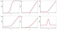
SignificanceIn recent years, with the development of computer technology, artificial intelligence has gradually penetrated many aspects of current human life. As the basic architecture of artificial intelligence, machine learning and neural networks have been given increasingly more attention to by researchers in recent years. At present, neural networks have been applied in matrix calculation, equation solving, data analysis, and many other fields, and have become a research field with great development potential in the 21st century. In conventional neural networks, linear functions are the primary mathematical tool. Nowadays, nonlinear activation functions (NAFs) can be employed to describe a large number of different systems, such as electric power systems, optical systems, economic systems, biological systems, computer networks, and communication systems. Nonlinear functions are a much more powerful mathematical tool than linear functions. Therefore, they are introduced into the neural networks to apply the neural networks to more nonlinear models.Currently, the application of nonlinear functions in neural networks is mainly realized through the nonlinear activation layers. The nonlinear activation layers of neural networks (NNs) can alter the linear transformation relationship beteween multi-layer networks, and thus enabling the NNs to solve more complex and advanced learning with flexibility. In pursuit of faster processing speed and lower energy consumption, optical neural networks (ONNs) have caught much attention from researchers in recent years. The response time of photons in ONNs is often picoseconds, and the energy loss of optical systems is often lower than that of electronic systems. Thus, the design of ONNs features high throughput and low power consumption. Therefore, except for electronic systems, photonic systems have shown a broad development prospect in computing. Additionally, the intelligent photonics represented by ONNs has also emerged and become an important development direction of information processing in the future. As an indispensable module in ONNs, a series of optical NAF devices have emerged. The nonlinear phenomena caused by the interaction between strong light and medium provide a powerful theoretical basis for applying NAF in photonic network architecture, and the integrated photonic device is also a feasible experimental platform for realizing NAFs. The NAFs broaden the application range of ONNs and provide a potential way to construct the next generation of integrated photonic devices on chip, which has a very broad development prospect. In this review, we summarize the recent studies that introduce optical NAFs to the systems and discuss their physical mechanisms and application capabilities. Meanwhile, this review also summarizes and discusses the challenges and future trends for the development in the research on optical NAF devices in ONNs, and provides outlooks related to such devices.ProgressMethods and principles for generating various NAFs under optic-electro-optic (O-E-O) and all optical regimes, which are the two major regimes reported so far, are summarized with more emphasis on the later regime. The applications for NAFs are also presented. NAF modulators under the O-E-O regime can be dissected into electro-absorption-modulators (EAMs) and electro-optic-modulators (EOMs), both of which have distinct merits and drawbacks. EOM utilizes a Mach-Zehnder interferometer (MZI) or the phase shifts in a micro-ring resonator (MRR) to modulate amplitude via interference. EAM can directly modulate the light amplitude without the need for interference and thus can be designed with a smaller footprint. However, the carrier-based EAM suffers from lower speed compared with the field-driven EOM. More specific comparison can be seen in the main content (Fig. 14). Besides the aforementioned categories, O-E-O modulation can also be achieved by doping the MRR to make its transmission sensitive to electrical currents and thus can engender different NAFs under different biasing conditions. NAF modulators under the all optical regime can be dissected into three major categories including customized materials, semiconductor optical amplifier (SOA), and MRR. Customized materials can be further divided into saturated absorption, reverse saturated absorption materials, electromagnetically induced transparency (EIT) materials, phase change materials (PCMs), and light matter interaction (LMI) material structure. Meanwhile, we provide the mathematical basis of the cross-phase and cross-gain modulation effects in SOA. Additionally, examples of how these nonlinear effects can be utilized to realize optical neural-network devices capable of simple operations are provided by chaining multiple semiconductor optical amplifiers together in certain configurations, such as optical "AND" logic gates and optical signal thresholders. For MRR, by utilizing the free carrier dispersion (FCD) effect or thermo-optical (TO) effect, NAFs with distinct responding times and threshold can be designed and optimized by incorporating materials like graphene or Ge and platforms like Si3N4. The Kerr effect in graphene can enhance the FCD in silicon, while Ge can be adopted to facilitate the TO process. In addition, the Si3N4 platform can be utilized to increase the processing speed by blocking FCD and turning to the Kerr effect. Performance parameters relevant to the threshold, responding time, and loss of these devices are also summarized and compared. The generated NAF can be leveraged to improve the performance in applications like pattern recognition and classification while adding reconfigurability to the NNs and facilitating real-time response NNs and efficient information processors. Finally, the prospects for NAF development, including reconfigurability, better performance, and developments in combination with quantum information processing are put forward.Conclusions and ProspectsNAFs in the optical regime have been realized with various schemes and enhanced the performance of ONNs. In summary, the performance of optical NAFs still needs improvement in terms of faster responding time or lower threshold and loss whether by incorporating new materials or by deliberately designing the SOA or MRR systems. As a result, they can better serve ONN to perform more accurate and complex tasks.
SignificanceOwing to the remarkable field confinement ability, surface plasmons have become an ideal platform for investigating light-matter interactions at the sub-wavelength scale. The intriguing properties make surface plasmons the fundamental block for future optoelectronic applications, including biomedical detection, photocatalysis, nanolaser, and data storage. Notably, the aforementioned fundamental and application research calls for surface plasmons with large tunability. Conventionally, the properties of surface plasmons can be tailored by changing the size, shape, environmental refractive index, and gap of the structure. However, these methods are usually static and lack of flexibility.Recently, the advance of light field manipulation has expanded the dimension of light utilization and provided rich and flexible strategies for regulating light-matter interactions. For example, through the amplitude, phase, and polarization modulation of the light field, a variety of super-resolution imaging techniques have been developed. Precise control of molecular rotation, dissociation, and ionization can be achieved by employing the time domain regulation of the light field. By controlling the coherence and polarization state of the light field, the conversion efficiency of nonlinear optical processes can be improved. Correspondingly, these methods for controlling the light-matter interactions have also been successively applied to surface plasmons, which open up a new way for exploring novel phenomena and developing related applications.ProgressThe eigen-response theory is first introduced to describe the polarization matching method to selectively excite plasmonic modes. We show the typical work on the tuning of dipole moment orientation [Fig. 2(b)] and the excitation of plasmonic dark modes (Fig. 3) with the aid of vector beams. The plasmonic mode controlling enables the generation of a strong local field to precisely manipulate the light-matter interactions at the single molecular level [Fig. 4(a)] and enhance the efficiency of surface-enhanced Raman spectroscopy [Fig. 4(b)]. Additionally, the nanosize particles with ultrasmall hot spots are trapped [Figs. 4(c) and 4(d)], and the optical upconversion frequency of a plasmonic octamer is tuned [Fig. 4(e)].Subsequently, the mechanism for controlling plasmonic mode coupling is explained in the frameworks of plasmon hybrid theory (Fig. 5) and coupled harmonic oscillator model (Fig. 6). Specifically, we present the work on controlling the bonding and antibonding modes of the plasmonic dimer with vector beams [Fig. 7(a)]. In 2010, Volpe et al. demonstrated a method to deterministically control the local field of the plasmonic nanostructure. They employed the optical inversion algorithm to superpose the Hermit-Gaussian beams with different amplitudes and phases to construct the vector excitation and successfully produce the target local field distribution as shown in Fig. 7(b). Meanwhile, we emphasize the excitation progress of single and multiple Fano resonances in highly symmetric plasmonic nanoclusters using the vector beams [Figs. 7(c) and 7(d)]. In addition, we show the applications of controlling plasmonic mode coupling in the optical binding force reversion [Fig. 8(a)], enhanced second harmonic generation [Fig. 8(b)], and the detection of structural defect and beam misalignment [Fig. 8(c)].Finally, the method to control the far-field scattering of plasmonic structures with vector beams is interpreted by combing Mie theory and Kerker condition. As an example, we show that the unidirectional scattering of a core-shell plasmonic nanosphere can be achieved by adjusting the phase differences and amplitude between electric and magnetic dipoles (Fig. 9). Interestingly, the tightly focused radially polarized beams can excite a spinning dipole moment in an Au nanosphere [Fig. 10(a)]. The polarization distribution at the focal plane allows for tuning the emission from a homogeneous to a unidirectional pattern by simply moving the particle relative to the beam axis [Fig. 10(b)], which is found to have an application in the directional coupling to a planar two-dimensional dielectric waveguide [Fig. 10(c)]. Additionally, Zang et al. demonstrate a method to realize the asymmetric excitation of surface plasmon polaritons (SPPs) by illuminating a pair of slot antennas with the Hermite-Gaussian beam [Fig. 10(e)]. They summarized the asymmetric intensity ratio of the SPP pattern as a displacement function of slot antennas [Fig. 10(f)], delayering a displacement sensor with angstrom precision.Conclusions and ProspectsWe briefly introduce the basic theory and physical mechanism of the interactions between vector beams and plasmonic modes and review the recent progress of plasmon mode excitation, coupling, and far-field radiation regulated by the vector beams. Furthermore, their applications in enhanced spectroscopy, nanometric optical trapping, and nano-displacement sensing are introduced. It is worth noting that the research on light field manipulation is still in a rapid development track, and some new types of light fields have been emerging, such as the superchiral optical needle, photonic skyrmions with topological features, and optical M?bius strips. These advances provide great opportunities for people to control plasmonic modes with extra freedom. Meanwhile, ultra-compact plasmonic structures represented by plasmonic nanocavities have emerged as a promising route to squeeze light into the true nanoscale level. It is foreseeable that if the merits of these two aspects are combined, one will have more abundant strategies to manipulate the optical properties of surface plasmons, ranging from the mode volume and optical chirality to the local optical density of the state. In this sense, it would open up a new avenue for studying basic physical phenomena such as strong coupling at room temperature, optical nonlinearity, and polarization-dependent optomechanics. Then, it will undoubtedly expand the applications of surface plasmons in information, energy, biology, and many other fields.
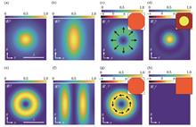
SignificanceOptical spin-orbit coupling is ubiquitous in nanoscale light-matter interactions. An in-depth study of these phenomena not only contributes to the discovery of new optical phenomena but also provides many opportunities for developing new technologies for light manipulation. In recent years, planar photonic devices such as geometric phase metasurfaces have shown many attractive applications, including multi-wavelength spin-dependent wavefront steering, spin-polarized photon generation, and spin-polarized thermal light emission. Most of these functions are achieved based on particularly designed nanostructures with certain types of spatial symmetry breaking, which aims to manipulate light in a subwavelength resolution and spin bases. In comparison, the interactions between light and disordered micro- and nanostructures also begin to catch our attention. However, the inherent randomness of disordered structures has made the research on spin-orbit coupling effects quite challenging, as stochastic processes must be considered in a statistic manner. Particularly, the emerging photonic spin Hall effect in random systems has not yet been fully understood. For instance, even though random geometric phase fluctuations and random vortices can both induce a photonic spin Hall effect, they have distinct physics origins. Thus, the underlined physics of the photonic spin split effects from different disordered geometric phases remains to be explored. This paper introduces the basic concept of the spin of light and spin-orbit coupling phenomena in different micro- and nano-optical systems and then focuses on analyzing the spin split effects of two-dimensional random systems, including anisotropic disorder, magneto-optical fluctuations, vortices, and random dipole radiation. Meanwhile, we attempt to utilize the photonic spin Hall effect in disordered systems as a potential means to precisely detect and manipulate two-dimensional magnetic and thermodynamic systems for the sensing and control of phase transition phenomena.ProgressA typical result of optical spin-orbit coupling is the photonic spin Hall effect (PSHE), which describes the spatial split between light that carries opposite spins. For example, PSHE occurs when a polarized Gaussian beam is reflected or refracted at the air-dielectric material interface [Fig. 2(b)]. It also emerges when the propagation direction of a polarized paraxial light is slowly changing in free space, where the light polarization will rotate accordingly. In 2009, Bliokh et al. coupled a paraxial beam into a cylindrical glass and realized a spiral trajectory of light through continuous total internal reflections on the inner surface of the cylindrical glass. The separation of spin-up and spin-down components of light is gradually amplified by accumulating geometric phases during this progress, and a PSHE was finally observed. In 2015, it was also demonstrated that the spin-momentum locking in the evanescent wave exhibits an inherent quantum spin Hall effect of light, which is a unidirectional spin transfer phenomenon of light along the interface surface. Around 2001, Hasman's group developed a set of planar geometric phase optical elements by spatially-varying subwavelength grating structures called Pancharatnam-Berry phase optical element [Fig. 2(d)], which is the earliest version of the geometric phase metasurfaces. Currently, geometric phase metasurfaces have been widely applied to construct versatile planar photonic devices for spin-based light manipulation and detection. Nonparaxial beams sometimes can behave counterintuitively. For instance, it has long been thought that linearly polarized dipole radiation does not carry angular momentum. However, recent theories and experiments have shown that the near-field of linear polarized dipole radiation can have a spin texture [Fig. 2(j)], and this nearfield spin information can be observed through waveguide coupling or scattering processes of isotropic nanoparticles. The interaction between light and disordered structures can produce novel phenomena and unpredictable results. For instance, disorders can be engineered to eliminate laser speckles for better wavefront shaping. In 2021, it has also been shown that, through the design of disordered noise, the information capacity limit of traditional metasurfaces can be broken, and wavefront control with more polarization degrees of freedom can be obtained. In 2017, Maguid et al. reported on photonic spin-symmetry breaking and unexpected spin-optical transport phenomena arising from subwavelength-scale disordered geometric phase structures. Weak disorder induces a photonic spin Hall effect, which is observed via quantum weak measurements, whereas strong disorder leads to random spin-split modes in momentum space, which is called a random optical Rashba effect. As the geometric phase of the metasurface to the spin of light has the same mechanism as the Berry phase, a similar spin Hall effect can be produced in principle. In 2019, Wang et al. observed photonic topological defects of bound vortex pairs and unbound vortices generated from a two-dimensional array of nanoantennas, which is achieved by randomly inserting local deformations in the metasurfaces. The spin Hall effect of light is established based on discrete topological structures, or subwavelength vortex and antivortex pairs. Light does not carry an electric charge and therefore does not directly interact with the magnetic field, but a magnetized medium does affect the light propagation path. In 2020, Wang et al. studied a stochastic photonic spin Hall effect arising from space-variant Berry-Zak phases, which are generated by disordered magneto-optical effects. This spin shift is observed from a spatially bounded lattice of ferromagnetic meta-atoms displaying nanoscale disorders. A random variation of the radii of the meta-atoms induces the nanoscale fluctuation. This spin separation of light is in analogy to a Stern-Gerlach experiment, and photons of opposite spin are deflected into opposite directions as they interact with a magnetic material with random spatial gradients. The luminescence of quantum dots, 2D semiconductor materials, perovskite particles, and some atoms or molecules can be considered as dipole radiation randomly generated in time and space. Efficient polarization and phase control of this kind of radiation requires novel metasurfaces that have strong mode coupling between nanostructures. To achieve efficient control of randomly radiated dipoles [Fig. 11(d)], Rong et al. designed a geometric phase defective photonic crystal. The insertion of geometric phase structures into a photonic crystal that has a bandgap realizes many local defect modes. These defect modes not only achieve localized light emission but also select radiation polarization. Via tight-binding coupling between nanoantennas, the light emitted by each dipole can propagate to neighboring nanostructures to obtain a geometric phase accumulation that radiates into space with a predesigned spin-dependent momentum [Fig. 11(c)]. This configuration realizes efficiency polarization and momentum control of the light from random emitters.Conclusions and ProspectsAs we have witnessed over the past two decades, optical spin-orbit coupling is ubiquitous in many optical systems. An in-depth understanding of these phenomena not only contributes to basic physics understanding but also brings forth a diversity of applications. Nowadays, the development of nano-photonics enters a stage where higher information dimensionality, higher spatial-time resolution, and many other extreme conditions are required. One promising direction is utilizing high-quality factor metasurfaces that can manipulate the polarization and wavefront of light beyond lasers, such as thermal light and quantum emitters. The other direction is to combine spin-optics and nano-magnetism. In particular, magnetic phenomena, such as those in magnetic metasurfaces or artificial spin ice, can be potentially detected by PSHE and quantum weak measurement. Finally, an optical means is provided to detect and manipulate the magnetic ordering and phase transition in correlated physical systems.
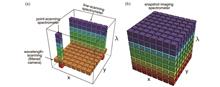
SignificanceSpectrum generally refers to the electromagnetic wave spectrum in the wavelength range from ultraviolet to infrared bands, containing rich information about the interaction between matter and light waves. Spectrum is also called the "fingerprint" of matter. Spectral imaging can obtain three-dimensional data cubes containing the spectral information of each point in the two-dimensional image, which surpasses the perception ability of human eyes, and it thus has important application prospects in many fields such as disease diagnosis, precision agriculture, food safety, astronomical detection, and face recognition.According to the methods of data acquisition, spectral imaging can be divided into four categories: point scanning type, line scanning type, wavelength scanning type, and snapshot type. Traditional spectral imaging technology generally adopts the mode of spatial scanning or wavelength scanning, which fails to obtain the real-time spectral information of each pixel in the field of vision. In recent years, new single-point spectrometers based on computational spectral reconstruction have made a breakthrough in miniaturization, but there is no report about snapshot spectral imaging based on the above scheme. There is no research scheme for snapshot spectral imaging that can achieve high spectral accuracy, high spatial resolution, and high imaging speed simultaneously.For the spectral imaging scheme based on metasurfaces, different metasurface units with different structure parameters are designed to realize rich broadband modulation on the spectra of incident light at each spatial point. The modulated light signal is detected by the image sensor, and the spectral information of incident light is obtained by computational reconstruction. The number of metasurface units can be significantly smaller than that of wavelength channels, which effectively reduces the volume of a single microspectrometer. Spectral imaging can be realized through the periodic array of the computational spectrometer, which has the advantages of high design freedom, high integration density, and low-cost mass production.ProgressIn 2022, we reported the world's first real-time ultraspectral imaging chip based on regularly shaped metasurface units. The designed metasurface units contain five types: round hole, square hole, cross hole, and square and cross hole after 45 degrees of rotation (Fig. 4). The real-time ultraspectral imaging chip reduces the size of a single-point spectrometer to less than 100 μm and can obtain spectral information of more than 150000 spatial points in a single shot. In other words, more than 150000 (356×436) micro spectrometers are integrated on a chip with a size of 0.5 cm2, and the operational wavelength band of each microspectrometer is 450-750 nm. The measured wavelength accuracy of monochromatic light is 0.04 nm, and the spectral resolution is up to 0.8 nm. In order to break through the design restriction of regular shapes, we propose a design method of freeform-shaped metasurface units. The freeform shapes are generated by grid partitioning, random distribution of grid values, filtering, and binarization. The corresponding design freedom is expanded by 2-3 orders of magnitude compared with that of regular shapes. Thanks to the expansion of design space, the performance of ultraspectral imaging chip based on freeform-shaped metasurface units is further improved, with a wavelength resolution up to 0.5 nm (Fig. 5). In terms of spectral image reconstruction algorithm, we propose to use ADMM-net, a deep unrolled neural network based on ADMM iterative algorithm, to realize fast spectral image reconstruction. A single reconstruction only takes 18 ms, and the reconstruction speed is improved by about 5 orders of magnitude compared with the traditional point-by-point iterative spectral reconstruction algorithm. We also discuss the application prospects of metasurface spectral imaging chips in the brain imaging of living rats, face anti-counterfeiting recognition, automatic driving, and other fieldsConclusions and ProspectsWe summarize the work related to metasurface spectral imaging chips from the basic principles, structural design, reconstruction algorithms, and potential applications. In the future, metasurface spectral imaging chips with the advantages of high precision, low cost, and mass production are expected to become the basis for the development of artificial intelligence and big data. Further optimization directions of metasurface spectral imaging chips include improving the spectral image reconstruction algorithm and reducing the angle sensitivity of metasurface units.
SignificanceHigh-Q resonances that confine the light energy at subwavelength scales have applications in various fields such as micro/nano-lasers, fluorescence enhancement, and optical sensing. Extreme light localization has been realized by surface plasmons squeezed in plasmonic nanogaps, whereas there is intrinsic energy dissipation by electron oscillations on metal surfaces. In contrast, high-index dielectric nanostructures supporting Mie-type electric and magnetic resonances exhibit low optical dissipation but only moderate field confinement. When plasmonic or high-index dielectric nanoparticles are arranged into periodic arrays, diffractive coupling in the plane of periodic arrays may occur. This can suppress the radiative damping of individual nanoparticles, and produce surface lattice resonance (SLR) modes with significantly higher (|E|2/|E0|2>103) field enhancements and much higher quality factors compared with isolated nanoparticles.The last two decades have seen significant progress in SLRs supported by metallic and high-index dielectric nanoparticle arrays under normal incident excitation. However, due to limitations in the involved materials and available nanofabrication methods, there is still a series of challenges in achieving a high Q-factor in the visible regime, especially in asymmetric refractive-index environments. Thus, it is necessary to summarize the existing studies to guide the future development of this field more rationally.ProgressWe first introduce the basic properties of SLRs in metallic and high-index dielectric nanoparticle arrays under normal incident excitation. The periodic lattices are usually generated by various top-down lithography methods. The difficulty in experimentally achieving SLRs with a high Q-factor from noble metal nanoparticle arrays is that the precise fabrication of defect-free nanoparticle arrays is hard. One strategy to overcome optical dissipation and reduce the linewidth of SLRs is to shrink the particle size relative to the lattice spacing. Reshef et al. at the University of Ottawa reported a Q-factor of 2340 in the telecommunication C band, and this is the ever reported highest value (Fig. 2). Another strategy is to make the particles smooth and uniform. Odom et al. at Northwestern University reported that thermal annealing can improve the uniformity, surface roughness, and crystallinity of metal nanoparticles produced by physical vapor deposition methods, which can lead to SLRs with dramatically improved Q factors (Fig. 3). Nie et al. from Fudan University proposed a method to produce metal nanoparticle arrays by combining solvent-assisted soft lithography and wet chemical with annealing processes, and thus a metal deposition process in a vacuum is not required (Fig. 4). Furthermore, SLRs can also be supported by arrays composed of complex basis or localized surface plasmons with multipolar characteristics, and these arrays show much richer optical responses compared with arrays with only one particle in a unit cell (Figs. 5 and 6). Arrays of high-index dielectric nanoparticles can support SLRs with characteristics of magnetic dipole (MD) besides electric dipole (ED), and both types of SLRs can be tuned independently (Fig. 7). By choosing lattice periods independently in each mutually perpendicular direction, Babicheva et al.from Georgia State University found that it is possible to make the ED-SLR and MD-SLR overlapped in a certain spectral range, which leads to the resonant suppression of the backward scattering (lattice Kerker effect).Subsequently, we summarize the progress in achieving high-Q SLRs based on mirror-backed high-aspect-ratio dielectric nanopillar arrays in asymmetric refractive-index environments (Fig. 9). In this hybrid system, dielectric nanopillars are arranged periodically on an optically thick metal film, which blocks the light transmission completely. Therefore, the issue of a symmetric dielectric environment between the substrate and the upper cladding does not exist, in contrast to the requirement of a symmetric environment for realizing sharp lattice resonances in all-plasmonic or all-dielectric systems. Meanwhile, the electric field enhancements are comparable to lattice plasmon modes from arrays of noble metal nanoparticles, but with strongly reduced plasmonic dissipation, since the enhanced fields are away from the metal surface. The narrow linewidth resonances can be tuned over a wide wavelength range from ultraviolet to mid-infrared by simply scaling the dielectric lattices and combining them with appropriate highly reflective metals. Additionally, numerical simulations show that it is possible to achieve a Q-factor of tens of thousands on this hybrid platform (Fig. 10).Conclusions and ProspectsSLRs arise from the diffractive coupling in periodic arrays, which can theoretically achieve a high Q-factor and greatly enhance the interactions between light and matter in the background media. This prominence has brought about the development of potentially practical devices for optoelectronics, biosensing, and other applications, using common materials such as noble metals and transparent dielectrics. Nanoparticle arrays of other functional materials like magnetic metals and newly emerging materials such as two-dimensional layered materials still need new design principles to mitigate their intrinsic optical dissipation to achieve high-quality surface lattice resonances with fascinating properties.
SignificanceThe rapid development in fields such as artificial intelligence, autonomous driving, and big data has brought higher demands for computational tools due to the massive amount of data involved. In recent years, with the development of ultra-large-scale integrated circuits, the volume of electronic computers has been significantly reduced, and the data processing speed has been greatly improved. However, electronic devices are gradually constrained by physical limitations such as quantum effects, which slow down the improvement speed of low-power and miniaturized digital computing circuits. In addition, traditional analog signal processing requires processes such as analog-to-digital conversion, signal processing units, and digital-to-analog conversion. The inevitable conversion delays and high-power consumption of electronic devices make traditional analog computing incapable of large-scale information processing. Therefore, researchers are devoted to developing new computing systems to overcome the limitations of traditional electronic computing systems. One of the technologies that has attracted significant attention is the construction of all-optical systems for information transmission and processing using optical signals as carriers.Optical information processing technology has attracted increasing attention due to its advantages such as ultra-high speed, large bandwidth, and low loss. People have attempted to introduce optical methods to improve the performance of information processing and have successfully designed various optical analog computing devices. Compared with electronic signal processing systems, optical signal processing can be categorized into digital computing and analog computing. The earliest digital computing of optical signals uses a liquid crystal spatial light modulator based on optoelectronic mixing for logical operations. Optical analog computing does not involve optoelectronic conversion and can directly manipulate optical signals in time and space domains. Due to the parallelism of physical processes such as light field promotion and interference in space, spatial optical analog computing offers advantages in information processing such as ultra-fast speed, high throughput, and low energy consumption. These attributes highlight its significant potential for applications in image processing, edge detection, and machine learning.ProgressTraditional spatial optical analog operations often employ the Fourier optical 4f system, which involves components such as lenses and filters. However, in recent years, the rapid development of micro-nano optics and fabrication processes has made it possible to realize spatial analog computing using devices at sub-wavelength scales. This opens up possibilities for miniaturization, on-chip integration, and integration of optical computing systems. At present, research on spatial optical analog computing primarily focuses on achieving spatial differentiation, integration, and equation solving. The main design principles can be classified into three categories: effective medium theory, resonance principle, and non-resonance principle (Fig. 1). Spatial analog computing can be achieved by integrating metasurfaces and GRIN lenses into a 4f system. By designing the spatial distribution of transmission (or reflection) rates of the metasurface, researchers can obtain the spatial spectral transfer function for the desired mathematical operations. However, this method requires the introduction of spatial Fourier transform and inverse Fourier transform, resulting in larger device dimensions. Another approach involves constructing a multilayer flat-stack structure using multiple materials, where various spatial optical analog computations can be achieved by adjusting the refractive index and thickness parameters of each layer (Fig. 2). Devices designed based on the equivalent medium theory have complex structures and pose challenges in practical fabrication. In a resonant system, the excitation of resonance requires momentum matching, which leads to different responses of the resonant structure to wavevector components in different directions of the incident light. This allows the spatial response of the propagating optical field in the structure to conform to specific optical simulation operations at certain frequencies, without the need for Fourier transform (Fig. 3). In contrast to the limited spatial bandwidth of resonant-based analog devices, under specific conditions in non-resonant systems, researchers can obtain the spatial spectral transfer function required for spatial analog operations based on the spin Hall effect, Brewster effect, and PB phase (Fig. 4). Spatial optical analog computing enables high-speed, high-throughput, and low-power information processing. Spatial differentiation and convolution operations can be directly applied to image edge detection and are promising for applications in pattern recognition, machine vision, and other fields (Fig. 5). Finally, the existing challenges and research prospects of spatial optical analog computing are discussed.Conclusions and ProspectsWe summarize the development of optical spatial analog computing and focus on the research progress and applications of optical spatial analog computing with metasurfaces in different theoretical models and systems. By incorporating artificial nanostructures to replace conventional large-scale optical components, metasurfaces enable the development of miniaturization and integration of spatial optical analog computing devices. Furthermore, we analyze the latest advances in spatial optical analog computing based on physical effects such as spin-orbit coupling and topology, which present novel avenues for achieving ultra-wideband and high-speed information processing. Lastly, we discuss the existing challenges and research prospects associated with optical spatial analog computing, shedding light on future directions for this field. With the development of information technology and the increasing demand for processing performance, optical information processing methods are gradually emerging. The design and implementation of various optical analog computing devices have become increasingly important for technological development and performance improvement. Spatial optical analog computing combined with metasurfaces has made unexpected progress, but it still suffers from some challenges such as the fabrication technology of metasurfaces, energy efficiency of optical analog computing, and reconfigurable computing. In the future, spatial analog computing combined with metasurfaces will unveil more innovative approaches, promoting the development of spatial analog computing from simple to complex. With continuous innovative advances in technology, combining various computing devices and achieving multi-functional optical computing chips may further boost fields such as high-throughput optical communication and optical imaging in the future.
SignificanceAs a layer of artificially designed two-dimensional planar structure, the metasurface provides a new platform for the miniaturization and integration of optical devices. In recent years, with the continuous development of this field, a variety of optical mechanisms and optical functional devices based on metasurfaces have been proposed. Despite their seemingly diverse functionalities, they can be all attributed to the control of different degrees of freedom in the Jones matrix. The Jones matrix is commonly employed to describe the ability of optical devices to control polarization, amplitude, and phase of light, with a maximum number of eight degrees of freedom. Especially, more controlled degrees of freedom lead to diverse functionalities that can be achieved. For example, a single degree of freedom in the Jones matrix can be adopted for anomalous transmission. By increasing to two degrees of freedom, such as independent control of amplitude and phase of a specific component of the Jones matrix, the integration of color printing and holography can be realized. From the perspectives of the degrees of freedom in the Jones matrix, we classify and summarize the designs and applications of metasurface research in recent years to help researchers better understand the physical mechanisms of different functionalities of metasurfaces.ProgressOur study focuses on the designs and applications of metasurfaces from the perspectives of the degrees of freedom in the Jones matrix. We firstly argue that all the functionalities of metasurfaces can be categorized into different degrees of freedom in Jones matrix and the more controlled degrees of freedom lead to diverse functionalities that can be realized (Fig. 1). Each component of the Jones matrix has two terms of amplitude and phase. Therefore, different mechanisms to control the phases including the geometry phase, resonance phase, and propagation phase are introduced to realize one degree of freedom (Fig. 2), which can be utilized for functionalities of metalens, hologram, and anomalous transmission. By changing the size of nanorods or nanodisks, the amplitude can also be controlled. Next, we show how to employ a simple structure of nanorod to construct multiple degrees of freedom in Jones matrix, including two (Fig. 3), three (Fig. 4), four (Fig. 5), six (Fig. 6), and eight (Fig. 7). Meanwhile, the possible applications are provided.Conclusions and ProspectsWe categorize and summarize the design methods of metasurfaces with different optical functionalities based on their degrees of freedom in the Jones matrix to provide different perspectives for the metasurface field. Although the highest number of degrees of freedom of eight in the Jones matrix has been realized, the following points can be explored. First, new optical multifunctional devices should be designed by integrating various functionalities based on the multi-degrees of freedom metasurfaces. Second, the optical performance of metasurface devices with multiple degrees of freedom should be improved. Third, the Jones matrix should be extended to the wavelength dimension to enable multi-wavelength and multi-degrees of freedom control of light fields. With continuous research and deepening exploration, the field of metasurfaces will advance with a wider range of practical applications.
SignificanceHow to better confine and manipulate light has always been an important research topic in optics. Resonant states in optical fibers or photonic crystals are typical designs for confining light, but due to the existence of leakage, the light confinement in these ways is not perfect, and light transmission in these structures will inevitably cause loss. As the loss generation will reduce the interaction efficiency between light and matter, a new method is needed to confine light more effectively and further reduce the loss. The bound state in the continuum (BIC) is a special eigenstate different from the extended state and leaky state in the continuum. It is located in the frequency range of the continuum with strong locality and does not radiate energy into free space. In 1929, von Neumann and Wigner built a mathematical model of artificial potential and discovered the existence of BIC for the first time. After that, BIC research has been vigorously developed, and the existence of BIC has been found in the fields of electromagnetics, nuclear physics, and acoustics. In 1985, Friedrich and Wintgen proposed a method to construct BIC. By adjusting the structural parameters, the eigenstates are coupled at the same position to make the loss of one eigenstate close to 0, and it is transformed into a BIC. The BIC generated by this method is also called Friedrich-Wintgen BIC. Fabry-Pérot BIC occurs when two eigenstates are not coupled at the same location. Designed optical structures can generate BIC, and these structures are usually periodic. By adjusting the structural parameters and material properties, BIC of specific frequency can be generated. For example, metasurfaces and plasmons are commonly employed structures to realize BIC. In 2011, Plotnik et al. adopted one-dimensional optical waveguide to observe the symmetrically protected BIC in the experiment for the first time.Optical BIC has two important advantages, including the near-infinite quality factor and the ability to generate far-field vortex singularities. These properties help generate sharp resonances with high quality factors in subwavelength-scale optical structures and can emit vortex light without the help of three-dimensional structures. This is conducive to constructing ultra-thin integrated optical components in the future, and enhancing the interaction between light and matter (such as nonlinear effects and quantum effects), with important potential in optical imaging and information transmission. Therefore, BIC has become a popular research direction in photonics and is studied in various photonic systems such as photonic crystals, metasurfaces, and plasmons.ProgressThis paper first introduces the taxonomy of photonics BICs. According to the differences with the far-field decoupling method, it is divided into two types of symmetry-protected BIC (Fig. 1) and accidental BIC (Fig. 2). Symmetry-protected BIC originates from symmetry mismatch, and accidental BIC originates from far-field interference cancellation of radiation components. Accidental BIC is divided into Fabry-Pérot BIC, Friedrich-Wintgen BIC, and single-resonance BIC according to the different radiation channels producing interference destructiveness. Fabry-Pérot BIC is produced by the coupling of two modes at different positions, Friedrich-Wintgen BIC by the coupling of two modes at the same position, and single resonance BIC by the coupling of different waves in the same mode. Then several commonly utilized theoretical models for explaining BIC are introduced (Fig. 3), including energy band theory, temporal coupled-mode theory, and multipole analysis. These theoretical models provide different perspectives to explain the physical mechanisms of BIC. Finally, the existing applications of BIC in photonics are introduced. For example, BIC is employed to enhance the nonlinear effect to realize laser emission and high-order harmonic generation (Fig. 4). Polarization control and chirality enhancement are realized by exploiting the vortex singularity properties of BIC (Fig. 5). Filtering and sensing are performed with the help of the sharp resonance peak characteristics of BIC with high quality factors (Fig. 6). Additionally, since BIC in the optical waveguide can realize efficient optical signal transmission, they are of application significance in photonic integrated circuits (Fig. 7).Conclusions and ProspectsIn summary, due to their ability to greatly enhance the interaction between light and matter, and control the outgoing light with extremely low energy loss, BIC has been studied in many optics fields, and various theoretical models for interpreting BIC generation have also been continuously developed and improved. At this stage, BIC still has bottlenecks such as difficult structure processing and design, and is expected to gradually make breakthroughs in the future.
SignificanceIn the 20th century, the research of the Fabry-Pérot (F-P) cavity mainly focused on basic optical properties and light source stabilization technology. However, with the development of quantum optics and nanotechnology, the research field of F-P microcavity has expanded rapidly in the 21st century. Nowadays, F-P microcavity is not only employed as an optical measurement tool, but also an important platform for studying the light-matter interactions to realize accurate parameter measurement, biological detection, and regulation for multi-dimensional light fields.The F-P microcavity is an ideal tool for measuring the frequency of the light source and stabilizing the laser frequency due to its interference properties. The spectrometer based on the F-P microcavity can achieve very accurate spectral resolution, which can meet the demand for a wide range of fields from astronomical observation to optical fiber communication.In terms of light-matter interactions, the F-P microcavity provides an ideal platform for exploring the coupling of photons and matter quantum systems. The photons in the microcavity can be strongly coupled with the material quantum systems such as atoms, molecules, or quantum dots, leading to some new physical phenomena. This provides possibilities for the development of new technologies such as quantum information processing based on light and ultra-low threshold lasers.In precision parameter measurement, F-P microcavity is widely applied to measure physical parameters such as temperature, pressure, refractive index, and pressure due to its high sensitivity to small changes in the environment. By accurately measuring the changing interference mode of light in the microcavity, accurate information about the microcavity environment can be obtained to achieve a very accurate measurement. In biological detection, F-P microcavity is adopted to detect the characteristics of cells, viruses, proteins, and other biomolecules due to its high sensitivity to small changes in tissues. This is of significance for early diagnosis of diseases, pathological research, and other applications in the biomedical field. Additionally, F-P microcavity also plays an important role in multi-dimensional light field control by precisely controlling the microcavity.ProgressFirst, the principle of the F-P microcavity is introduced based on thin-film optical theory (Fig. 1). The work progress of linear variable filter, integrated F-P filter, and reconfigurable spectrometer based on the F-P microcavity is presented according to the sequence of research development. The research team at Changchun Institute of Optics, Fine Mechanics and Physics, Chinese Academy of Sciences, has carried out extensive research and application of linear gradient filter. In integrated F-P filter, Wang et al. from Shanghai Institute of Technical Physics, Chinese Academy of Sciences, proposed a method of combinatorial etching and deposition (Fig. 4) to prepare integrated F-P filter. As technology advances, nano-imprint lithography and grayscale lithography have also been applied to fabricate integrated F-P filter. F-P microcavities can be integrated with detectors, and the resulting spectrometers feature small size, light weight, and high stability. To overcome the difficulty in achieving high resolution in spectrometers based on F-P microcavities and the associated manufacturing challenges, spectral reconstruction algorithms have been introduced to significantly improve the spectral resolution of spectrometers. In the interactions between photons and low-dimensional materials in an all-dielectric F-P microcavity, low-dimensional semiconductor lasers based on all-dielectric F-P microcavities are introduced first. Based on the theory of cavity quantum electrodynamics, the weak and strong coupling interactions between light and low-dimensional materials are discussed. With the developing fabrication technology of two-dimensional materials, researchers continued to deepen the research on light-material interactions in microcavities, and strong coupling phenomena and research related to exciton-polariton lasers have gradually been reported.In F-P microcavity applications, its application in precision parameter measurement is first introduced. Due to the high-quality factor and strong resonance effect of the F-P microcavity, researchers have achieved precision measurement of parameters such as environmental refractive index, temperature, humidity, pressure, and sound through the utilization of optical fibers and corresponding sensing materials. Meanwhile, the teams of Lu Wei and Wang Shaowei from Shanghai Institute of Technical Physics, Chinese Academy of Sciences, have further expanded the measurement field to achieve measurements of the complex refractive index of low-dimensional materials of tiny dimensions. In biological detection, the F-P microcavity can be employed to reveal the characteristics of cells and biomolecules, describe changes in internal molecular interactions, and aid in the detection, identification, and imaging of biomolecules. In multi-dimensional optical field control, by combining the high quality factor of the F-P microcavity, narrow spectral features, and introduction of emerging micro/nano devices such as metasurfaces, it is possible to achieve control and generation of polarization/spectrum, beam shaping, and vortex light fields. This lays the foundation for high-performance and multi-functional optical field control.Conclusions and ProspectsThis review summarizes the research progress in optical field control in F-P microcavities over the past 20 years. The research is focused on the introduction of spectroscopic structures and spectroscopic detection applications based on F-P microcavities, the interaction study of photons with low-dimensional materials in F-P microcavities, and potential applications of F-P microcavities in precision measurement of parameters, biological detection, and multi-dimensional optical field control. Further exploration and in-depth studies are essential for issues such as optimizing the design of the microcavity, accurately manipulating its parameters, and enhancing its stability. The research field of F-P microcavities will be further expanded.
SignificanceAs a classical physical phenomenon, the Brewster effect describes the zero-reflection behavior of a polarized planar electromagnetic wave impinging on the surface of a linear homogeneous isotropic non-magnetic media. Traditionally, this classical effect is usually restricted to particular incident angle and polarization due to the scarcity of natural material with ideal magnetic response, and the research on generalizing the classical Brewster effect was only of theoretical interest. Nevertheless, the advent of metamaterials and metasurfaces brings new vitality to the research field of the so-called generalized Brewster effect (GBE), where many efforts have been done for seeking zero-reflection of planar wave at any frequency, any polarization and any incident angle. The physical implementation of GBE has enabled people to gain a greater degree of freedom for modulating electromagnetic waves in a wide range of frequency, polarization and angle of incidence. Therefore, the GBE has been demonstrated to have important applications in many fields such as wireless communications, phased array antennas, nanophotonics and even chemical sensing.So far, both physical mechanisms and experimental methods of GBE have been explored in a variety of physical systems. Many theoretical methods for explaining the GBE mechanism have been proposed, such as optical filter theory, transfer matrix method, molecular optics method and so on. However, most of these methods are either lack of intuitive physical understanding or only applicable to specific physical scenes, and thus cannot provide useful guidelines for GBE design. Moreover, in the past research, the realized GBEs are often fixed at some frequencies or incident angles and untunable, limiting their application in varied situations. Hence, a universal and intuitive GBE design principle is highly demanded, and it is important to summarize the existing research on both the general design method and arbitrarily tunable GBE realization. Furthermore, the application aspect of GBE is rarely discussed in literature, and it is worth discussing some novel applications to fill this gap.ProgressIn this article, the recent work of our group for realizing tunable dual-polarized GBE is introduced, and two novel applications in the field of millimeter-wave communication and phased array antenna are presented. First, the mechanism and implementation of various published GBE systems are summarized, among which a physical interpretation based on the generalized Kerker effect (GKE) is discussed in detail due to its profound physical insight (Fig. 1, Fig. 2). From the perspective of GKE or multipole destructive interference, a simple and universal design principle for implementing GBE is proposed (Fig. 3), that is, we can construct artificial multipoles to coherently eliminate the radiation of the multipoles intrinsic in the original system at some particular angles. Under the guidance of this principle, we proposed a metasurface composed of artificial metallic structure, and realized an arbitrarily tunable GBE in the microwave band (Fig. 4), where the zero reflection can be realized at the same frequency and same incident angle for the two different polarized incident waves. After that, an application in the scenario of 5G millimeter-wave communication is presented, that is, we designed a single-layer metasurface for realizing dual-polarized ultra-wide-angle high transmission (Fig. 5) and a near-isotropic electromagnetic window suitable for engineering application in 5G communication (Fig. 6). Besides, we noted the consistency between the ideal planar phased array model and the Fresnel reflectance model in the sense of physical image, and pointed out the implications of GBE for wide-angle impedance matching of phased array antennas (Fig. 7). Under this heuristic design idea, a planar slot antenna array with ultra-wide angle scanning performance is presented and discussed (Fig. 8).Conclusions and ProspectsThe realization of generalized Brewster effect provides the possibility for people to arbitrarily modulate electromagnetic waves of vatious frequencies, polarization and incident angles, and is expected to provide solutions for challenges in both academic and engineering aspects, such as electromagnetic window, wide-angle scanning phased array, angle filter and so on. So far, the GBE has been well studied both theoretically and experimentally, but some research gaps still exist. To sum up, in-depth study is still needed in this field and the future directions may include: the realization of wide-band wide-angle GBE; the application in designing electromagnetic window with angle filter characteristics; the application in designing wide-band wide-angle phased array antennas and the influence of GBE metasurface on antenna performance, and others.
SignificanceModulating the motions of photons through topological structures plays a primarily vital role in both scientific research and practical applications, which leads to a new but thriving study direction, namely topological photonics. Flexible topological phases and robust topological states provide an unprecedented perspective to the abundant physics phenomena generated by vector electromagnetic fields with spin-1. On the other hand, photonic artificial microstructures, such as metamaterials and photonic crystals, can be gradually perceived as substitutes and even upgrades of some complex topological models in condensed matter physics, which mainly rely on their rich state control mechanisms and highly customized design degrees of freedom. In this research process, some properties of optical topological states are utilized to overcome some engineering problems, including exploiting robustness to eliminate the scattering losses caused by defects and disorders. In view of the early success of Hermitian topological systems, recent focus has been laid on non-Hermitian topological systems described by non-Hermitian Hamiltonians. Especially, when the Hamiltonian of the system satisfies the parity-time (PT) symmetry, its eigenvalues are pure real, which corresponds to a unique non-Hermitian system with highly sensitive exceptional points (EPs) in the parameter space and novel skin effects in edge modes.In the past decade, wireless power transfer (WPT) and sensing become a hotspot, which triggers immense research interest in practical applications, including mobile phones, logistic robots, medical-implanted devices, and electric vehicles. For a standard WPT system, it is mainly composed of two coupled coil resonators, which are placed on the source and receiver sides, respectively. However, there are some aspects of these conventional WPT applications that should be noted. For example, the limitation of the coupling of evanescent waves and the inherent sensitivity to the transmission distance or structural disturbance restrict the structure sizes and application scenarios. With the development of WPT devices, efficient long-range and robust WPT is highly desirable but challenging. Recently, the non-Hermitian topological edge mode provides a powerful tool for near-field robust control of WPT. Therefore, it is critical to review recent works on high-performance near-field wireless power transfer and sensing systems with topological protection characteristics inspired by non-Hermitian topological effects.ProgressTopological edge states of dimers can provide a suitable platform for the study of robust WPT in the radio frequency (RF) regime. On the one hand, similar to the Domino structure composed of coupled resonators for long-range WPT, the topological dimer chain can be used to realize efficient long-range WPT. On the other hand, the edge modes in nontrivial dimer chains are topologically protected, and thus the corresponding WPT is robust against the disorders and fluctuations (Figs. 3-8).At the same time, a long-range WPT can be realized through a finite quasiperiodic Harper chain based on the ultra-subwavelength coil resonators. In addition, the distribution of the asymmetric topological edge states (TESs) in the Harper chain is observed from the local density of states (LDOS) spectrum (Fig. 10). Especially, using the asymmetric topological edge states, two Chinese characters composed of light-emitting diode (LED) lamps are selectively lighted up at both ends of the chain, which intuitively show the directional WPT in the topological Harper chain (Fig. 11). Moreover, in view of the robustness of topological edge states, the designed WPT device can be robust to the disorder perturbation inside the structure. The topological edge states for directional WPT not only extend previous research work on long-range WPT but also have a circuit structure that is easier to integrate and for active control. As a result, by adding electrical variable capacitance diodes into the system, the actively tuned transmission direction by modulating the external voltages applied in variable capacitance diodes (VCDs) is experimentally observed (Fig. 12).Moreover, the properties of the EP exist in a finite non-Hermitian topological circuit-based dimer chain (Fig. 13). The coupling between two edge states is presented, which is particularly relevant to the realization of second-order EPs. By adding loss and gain to both ends of the dimer chain, the non-Hermitian topological chain and the EP that satisfies PT symmetry (Fig. 14) can be obtained. In similar systems, topological edge states are highly sensitive to disturbances in the environment before and after the EP, which lead to new highly sensitive sensors with topological protection (Fig. 15). In sharp contrast to traditional sensors, this new sensor based on non-Hermitian and topological characteristics has unique advantages. It is immune from disturbances of site-to-site couplings in the internal part of the structure and is sensitive to the perturbation of on-site frequency at the end of the structure.Conclusions and ProspectIn summary, high-performance near-field WPT and sensing systems are realized with topological protection characteristics inspired by non-Hermitian topological effects. Especially, the one-dimensional system composed of resonant coils provides a simple but efficient platform to utilize the advantages of topological and non-Hermitian effects in practical applications. In addition, new topology structures with higher dimensions and higher orders are promising candidates to realize multifunctional WPTs in the future.
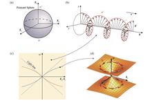
SignificanceArthur Ashkin was awarded the Nobel Prize in Physics 2018 for the invention of optical tweezers and their biological applications, which fulfilled the prediction of Ashkin "I think the field of biology may win a Nobel Prize for the great work done by optical tweezers". Optical tweezers have aroused extensive attention since they were born, which manipulate tiny objects by exerting optical forces. Till now, optical tweezers have made great achievements in the field of physics, chemistry, biology, medicine and nanotechnology.In the process of interaction between light and matter, the transfer of linear momentum and angular momentum can generate optical forces, while the angular momentum of light can also induce optical torques. Optical torques have been widely used in optical manipulation for their advantages of non-contact, small size and high precision. Optical torques provide another degree of freedom in optical manipulation, finding wide applications in biomedical, physical and quantum sciences, including the fundamental mechanical properties of biopolymers and numerous molecular machines that drive the internal dynamics of cells.On the one hand, optical torques endow biologists with a "microscopic hand" that can minimally manipulate organisms like a microscope because of their contactless nature. As a result, optical torques can control cells, viruses and other hard-to-control biological samples, avoiding potential sample damage and making many live experiments possible. Meanwhile, using non-contact capabilities, optical torques are able to drive the internal dynamics of cells without causing any damage. This can solve many thorny problems faced by biologists. On the other hand, optical torques are usually very small, down to the magnitude of pN?nm or even fN?nm, making them ideal for precise manipulation of small objects, such as rotating DNAs and proteins. With the support of such a precise tool, the characteristics of DNAs and proteins can be studied easier.Except for biology, optical torques also have great potential applications in physical applications. As a cutting-edge technology, optical torque wrenches have been used to measure the Casimir torque and explore the quantum properties of gravity. Besides, it is known that optical torque wrenches are the basis of optical tweezers' quantitative experiments and have been used in various optical tweezers experiments, such as precise torque measurement and liquid viscosity determination.In the past decade, the combination of optical torques with other technologies has further expanded the impact of optical torques in the field of biology and physics. For example, optical torques can be integrated with microfluidic systems. With the help of the transmission of fluid, optical torques assist optical tweezers capture the particle in the solution and transfer the angular momentum.ProgressIn this paper, we start by discussing the fundamentals and the conditions of two kinds of optical torques. By comparing the directions of optical torques and the angular momentum of the incident light, the optical torques can be classified as positive and negative optical torques. We discuss the mechanisms for the two kinds of optical torques in detail (Figs. 2-8). Then, we outline the traditional mechanisms for enhancing the optical torques, including spin-orbit coupling (Fig. 9), ring resonator (Fig. 10), and plasmonic structures (Fig. 11). Meanwhile, we introduce some leading-edge mechanisms for optical torques enhancement, like using super-hybrid modes from the combination of the electric toroidal dipole and magnetic multipoles (Fig. 12). Next, we review the physical and biological applications. In physical applications, we discuss the setup and theory of the optical torque wrench (Fig. 13) and micromechanics using optical torque, such as the Archimedes micro-screw (Fig. 14). In biological applications, we discuss the measurement of the biomolecule, like the characteristics of twisting in DNAs (Fig. 15), and we mention applications of optical torques in biorheology, biosensors, and micro-biorobots (Fig. 16). We culminate with a summary of the challenges in optical manipulation with optical torques, as well as the outlook of future developments, such as the torque sensing in biomedicine and light-driven biorobots.Conclusions and ProspectsThe capabilities of optical torques to capture, control, and rotate particles have brought more opportunities for optical manipulation, compared with the translational movement of earlier optical tweezers technology. However, optical torques still face many challenges in optical manipulation. For example, the optical torque is generally small, so it is difficult to control large-sized particles, and the rotation efficiency is low, which brings some difficulties to the light-driven rotating micromechanics. Fortunately, nontrivial theoretical studies of topological optical forces have been proposed recently, which introduce topological concepts to optical forces at bound states in the continuum. This offers opportunities to realize optical force vortices, enhanced reversible forces, and even negative torque for manipulating nanoparticles and fluid flow. In the future, optical torques caused by topological optical force can be studied further to enhance the optical torques. In addition, by designing the diffraction characteristics of the metasurface, the direction control of the meta-robot can be realized, so as to realize the multi-dimensional steering of the light-driven robot. It can be predicted that optical torques will be more widely utilized in biomedical and physical sciences and other fields.
SignificanceMicro-nano optical devices, resulting from the integration of photonics and micro-nano technology, are rapidly growing within the optoelectronics industry. These devices can effectively modulate light fields according to their design and have been widely used in fields such as photonic integrated chips, optical communications, optical storage, sensing imaging, display, solid-state lighting, biomedicine, and photovoltaic energy. As the applications for micro-nano optical devices continue to expand, there is an increasing demand for the development of micro-nano manufacturing technologies to support their production.A range of micro-nano manufacturing techniques is required to meet the writing requirements of different micro-nano optical devices. These techniques include direct laser writing (DLW), interference lithography, mask projection lithography, nanoimprint lithography, electron beam lithography, and ion beam lithography. Interference lithography can achieve rapid large-area writing through interference exposure but is limited in its ability to customize writing patterns, and it is difficult for writing aperiodic structures. Both mask projection lithography and nanoimprinting are well-suited for the fast fabrication of high-resolution features but require the prior fabrication of templates and offer limited flexibility in structure writing. Writing with focused charged particles (ions and electrons) can achieve resolution below 10 nm, but both electron beam lithography and ion beam lithography require a vacuum environment. They have high system costs and are not well-suited for writing three-dimensional structures.DLW technology based on two-photon polymerization (also known as two-photon direct writing) has emerged as an important technology for manufacturing micro-nano optical devices due to its submicron resolution, ability to write arbitrary three-dimensional structures, and cost-effectiveness. Two-photon polymerization exhibits nonlinear characteristics that can confine photochemical conversion to the central region where excitation light is focused. Complex three-dimensional structure writing can be achieved through the relative movement of any three-dimensional position between the laser focus and substrate. The exposed area of photosensitive material will undergo polymerization while unexposed areas can be dissolved in the developer and washed away during development, resulting in a microstructure on the substrate after exposure and development.Devices fabricated using two-photon direct writing primarily consist of polymer materials, with their composition largely dependent on the photoresist used. Photoresists can be liquid, gel, or solid and can be composed of organic molecules or organic-inorganic hybrids. Many types of polymers can be combined with new or active materials to achieve specific functions. The high degree of freedom in polymer material design and the flexibility of two-photon direct writing exposure have led to a widespread study of micro-nano optical devices based on two-photon direct writing. These devices have played an important role in diffractive optics, imaging optics, fiber optics, color optics, integrated optics, and optical data storage.As the applications for micro-nano optical devices based on two-photon direct writing continue to expand, there are increasing demands for improved performance from two-photon direct writing technology. In terms of writing resolution, two-photon direct writing is primarily limited by the diffraction effect of the optical system and the proximity effect in photoresist material. To further improve writing resolution, researchers have proposed a super-resolution DLW technology based on peripheral photoinhibition (PPI) inspired by stimulated emission depletion (STED) microscopy. This technology can overcome the diffraction effect and reduce the proximity effect. Super-resolution DLW technology can advance the fabrication dimension of two-photon direct writing to the nanometer scale and has been successfully applied in fields such as photonic metamaterials, optical data storage, and biological applications. In terms of writing throughput, two-photon direct writing is primarily limited by its single-focus serial writing mode. Compared with that of projection lithography, the throughput of two-photon direct writing is lower, and two-photon direct writing is not well-suited for large-area rapid manufacturing. Utilizing multi-channel parallel writing techniques can significantly enhance the writing throughput of two-photon direct writing processes. This advancement facilitates large-scale printing capabilities for micro-nano optical devices. The ability to achieve cross-scale fabrication with nanometric resolution and centimetric size is crucial for the mass production of large-area and high-quality micro-nanostructure devices.ProgressBuilding upon two-photon direct writing technology, the State Key Laboratory of Extreme Photonics and Instrumentation of Zhejiang University along with Zhejiang Laboratory have developed several advanced techniques to achieve super-resolution and high-throughput writing in two-photon direct writing. These techniques include single-color PPI lithography, two-focus parallel PPI lithography, and high-speed parallel two-photon direct laser writing lithography. We focus on the applications of these techniques in the fabrication of micro-nano optical devices. First, we provide an overview of the principles of two-photon direct writing (Fig. 1) and its applications in diffractive optical devices (Figs. 2-3) and optical fiber integrated devices (Figs. 4-5). We then introduce the principles of single-color PPI lithography (Fig. 6) and discuss our research on the applications of super-resolution direct laser writing in nanophotonic devices, including metasurfaces (Figs. 7-8) and photonic crystals (Fig. 9). We also summarize the current fabrication methods and printed sizes of photonic crystals (Table 1), indicating the extremely high resolution of single-color PPI lithography. Finally, we present the technical advantages of high-precision and high-throughput DLW technology for manufacturing centimeter-scale micro-nano optical devices.Conclusions and ProspectsThe technology proposed and developed by our group exhibits nanoscale resolution and centimeter-scale cross-scale processing capabilities. This technology has been successfully applied to manufacture various micro-nano optical devices. We continue to explore new technologies and methods to better meet the demands of micro-nano optical device manufacturing. We anticipate that DLW and its enhancement technologies will play a crucial role in advancing the field of micro-nano optical device fabrication in the near future.
SignificanceThe development of photonic integration technology provides an effective approach to constructing communication, sensing, computing, and information processing devices with high performance, low cost, scalability, and reliability. Among various material platforms, lithium niobate (LN) has long been considered one of the most suitable materials for realizing photonic integrated circuits (PICs). It possesses superior optical properties, including a wide transparent window (0.35-5 μm), large nonlinear/electro-optic coefficients, and strong acousto-optic effects. Significant progress has been made in the fabrication process of thin film LN (TFLN) wafers, which has laid a material foundation for manufacturing photonic devices with high refractive index contrast and strong light field confinement. To date, researchers have achieved a wide range of photonic integrated functional bricks on TFLN, such as modulators, optical frequency converters, splitters, quantum light sources, and delay lines. These devices have demonstrated notable photonic characteristics, including low transmission loss, high-speed controllability, efficient optical frequency conversion, and low energy consumption. However, due to the lack of optical gain characteristics in LN crystals themselves, it is challenging to directly fabricate essential components for on-chip integration, such as micro-lasers and optical amplifiers, on TFLN wafers.One approach to achieving optical gain on TFLN is by doping gain media within the TFLN film. Rare-earth ion-doped (REI-doped) TFLN has been employed to realize on-chip micro-lasers and optical amplifiers at different wavelengths, such as around 1550 nm and 1030 nm. The specific working wavelength is determined by the intrinsic optical spectra of the rare-earth-doped ions. Although active integration of TFLN photonic devices is still in its early stages, the exceptional optical properties of LN crystals, combined with low-loss photonic chip fabrication techniques and innovative device designs, will endow on-chip TFLN photonic devices with unparalleled scalability and exceptional functionality.In recent years, the combination of commercial TFLN wafers and low-loss LN photonic device nanostructuring technology has resulted in a series of high-performance photonic device applications. In less than a decade, several important manufacturing techniques for LN photonic chips have been developed internationally, enabling the realization of practical high-quality photonic chip prototypes. These techniques include focused ion beam fabrication of high-performance LN nanostructures, as well as the use of electron beam lithography or ultraviolet photolithography combined with ion etching to produce high-quality LN photonic chips. Additionally, the photolithography-assisted chemo-mechanical etching technology (known as PLACE) has emerged as a promising micro/nanofabrication technique.Thanks to the rapid advancements in high-repetition-rate and highly stable femtosecond lasers and large-stroke high-precision high-speed motion stages, the PLACE technique for fabricating active photonic devices on REI-doped TFLN has demonstrated both high processing efficiency while maintaining its inherent high-precision processing quality. Many corresponding advances have been achieved, which is important and necessary to summarize the existing research to guide the future development of this field more rationally.ProgressThe fabrication process of the PLACE technique is summarized (Fig. 1). The home-built ultra-high-speed high-resolution femtosecond laser lithography fabrication system is reported (Fig. 2). The demonstration of integrated active LN photonic devices such as on-chip tunable micro-lasers and waveguide amplifiers on REI-doped TFLN using the PLACE technique are comprehensively reviewed. Specifically, an erbium ion-doped LN waveguide amplifier with a maximum internal net gain exceeding 20 dB is achieved (Fig. 18), and an electro-optically tunable single-frequency laser in a high-Q LN microdisk is demonstrated with an ultra-narrow linewidth of 454.7 Hz (Fig. 5). We also achieve an electrically driven microring laser by monolithically integrating a diode laser (Fig. 10) and an erbium ion-doped TFLN microring laser (Fig. 3). A novel hybrid integration scheme of passive and active LN microdevices is performed using a continuous lithographic processing approach (Fig. 19 and 20). Lastly, we summarize the afore mentioned results and give an outlook on this vibrant and promising field of research.Conclusions and ProspectsThe utilization of PLACE technology for the fabrication of TFLN active photonic devices holds great importance. This cutting-edge technique, with its high processing efficiency, intrinsic high precision, and wafer-scale integration capability, enables the production of cost-effective and high-performance photonic devices. This breakthrough has the potential to revolutionize the field of photonic science and technology, promoting sustainable development across various scientific disciplines and applications such as high-speed communication, artificial intelligence, and precision measurement.
SignificanceMetal nanoparticles exhibit superior optical resonances, known as localized surface plasmon resonances, due to collective oscillations of free electrons during their interaction with incident light. These resonances enhance light absorption and scattering, making these nanoparticles highly efficient in interacting with electromagnetic waves. The tunability of plasmon resonances through nanoparticle size, shape, and composition further enhances their optical responses. As a result, plasmonic nanoparticles are valuable for applications such as sensing, imaging, and energy conversion.In addition to their optical resonances, metal nanoparticles also serve as acoustic resonators, capable of converting electromagnetic energy to mechanical energy through photoacoustic and optoacoustic effects. Excitation of metal nanoparticles by short laser pulses leads to rapid increases in electron and lattice temperatures, which generates thermal expansions and particle vibrations. The mechanical vibrations in metallic nanoresonators are influenced by factors such as nanoparticle size, shape, and surrounding environment. Accurate measurements of the acoustic vibrations provide insights into the mechanical properties of nanoresonators and the surroundings, with potential applications in nano-optomechanical devices, sensor technology, and photoacoustic imaging.The vibrational frequencies of metallic nanoresonators typically range from a few to hundreds of GHz. Ultrafast pump-probe spectroscopy has emerged as a powerful tool for investigating these high-frequency mechanical vibrations. Due to the large absorption cross-section of plasmonic nanoparticles, it is feasible to study the acoustic vibrations in metallic nanoresonators at a single-particle level. In such experiments, a pump laser excites mechanical vibrations in single particles, and a delayed probe laser monitors the dynamics of the vibrations with high temporal resolutions. The ability to perform single-particle studies of acoustic vibrations provides new opportunities for understanding the vibrational energy damping mechanisms and mode coupling effects.A significant issue related to metallic nanoresonators is energy loss, where the acoustic energy dissipates through both intrinsic and extrinsic damping pathways. Extending the vibrational lifetimes of acoustic nanoresonators is beneficial for nanomechanical spectrometry and sensing, vibrational coupling, and quantum state preparations. Many experimental studies primarily focus on the energy dissipation mechanisms in nanoresonators. Mass sensing, high-frequency biomechanics and bioimaging, and nanofluid mechanics are at the forefront applications of acoustic resonators with large vibrational quality factors.While metal nanoparticles have been extensively studied, exploring other materials platforms, such as 2D semiconductor materials and heterostructures, offers new avenues for studying and harnessing acoustic vibrations at the nanoscale. These materials possess unique mechanical and acoustic properties that can be tailored and engineered to present great opportunities for nanoscale acoustic research and device development.ProgressWe review the coherent acoustic vibrations of metallic nanoresonators and discuss their potential applications. First, we discuss the excitation mechanism of coherent acoustic vibrations in metallic nanoresonators, and the corresponding transient absorption microscopy measurements. Second, the acoustic vibrational modes and frequencies of several metallic nanoresonators (including nanospheres, nanorods, and nanoplates), and the correlations with particle sizes and shapes are described (Figs. 3-5). Then we give detailed discussions on vibrational strong coupling between metallic nanoresonators, from experimental measurements of various vibrational coupling systems to theoretical analysis of the coupling mechanisms and mode profiles (Figs. 6-9). Further investigations of strong phonon coupling between acoustic nanoresonators are essential for quantum phonon manipulations in plasmonics. Next, we provide a few examples of the potential applications of high-frequency acoustic nanoresonators, with special emphasis on nanofluidics (Fig. 10). The studies demonstrate that the standard continuum fluid mechanics assumptions are no longer applicable at the nanoscale, and viscoelastic effects and interfacial slip phenomena must be considered. The observed nanoscale fluid phenomena have broad significance for the description and understanding of nanofluidics. Finally, the discussions on future development and applications of high-frequency acoustic nanoresonators are presented.Conclusions and ProspectsThe study of acoustic vibrations in nanoresonators provides significant insights into the fundamental physics of nanoscale systems and opens up broad prospects for various applications, such as high-frequency biomechanics, nanofluid mechanics, and phonon frequency combs. Continuous research in this field has great potential for further discoveries and technological advancements.
SignificanceOptical scattering provides researchers with a wealth of information, including light intensity, phase, and polarization. Angle-resolved spectroscopy (ARS) is a powerful technique that measures the distribution of light intensity with angles or wavelengths. It plays a crucial role in obtaining important optical information to solve optical inverse problems and represent the properties of micro-nanophotonic materials.In optical inverse problems, ARS assists researchers in determining the morphological structures and optical constants of materials by analyzing the angle-dependent behaviors of scattered light. This technique is particularly helpful when traditional measurement methods, such as scanning electron microscopy (SEM) and atomic force microscopy (AFM), are not feasible. By solving optical inverse problems using ARS and inverse algorithms, researchers can gain a deeper understanding of the behavior of light in complex materials and systems. Additionally, it finds wide application in the semiconductor industry to detect defects in wafers and measure optical critical dimensions of optoelectronic components.ARS also enables researchers to represent the properties of micro-nanophotonic materials. It plays a crucial role in photonic crystal and metamaterial research. By measuring the angular dependence of light scattered or emitted by these materials, researchers can gain insights into their unique optical properties, such as band structure, dispersion, capabilities of light field regulation, and photonic density of states. This information is essential for designing and optimizing these materials for various applications, such as sensing, imaging, and light manipulation. Furthermore, the ability to control and manipulate light at the nanoscale has the potential to revolutionize photonics and enable the development of new technologies. Therefore, ARS is a powerful technique for investigating optical inverse problems and harnessing the optical properties of micro-nanophotonic materials.In recent years, various methods have emerged for generating angle-resolved spectra and processing data. Mechanical angle-scanning spectroscopy measurement and Fourier planar imaging represent the two primary methods employed. Urgent application needs have spurred the rapid proposal of abundant data analysis algorithms. However, it is important to acknowledge that each approach possesses its limitations and drawbacks. Therefore, the provision of a rational framework is imperative to summarize these methods and applications, guiding future advancements in the field.ProgressIn terms of generating angle-resolved spectra, two main methods will be introduced. The first method is mechanical angle-scanning spectroscopy measurement. Jér?me et al. developed the Mueller matrix scattering ellipsometry (MMSE), which enables scanning both inside and outside the incident plane (Fig. 2). Heather et al. employed the goniometric optical scatter instrument (GOSI) to obtain angle-resolved reflection for s and p polarizations of the target (Fig. 3). Chen et al. developed the tomographic Mueller-matrix scatterometer (TMS), where the incident beam is focused on the rear focal plane of the objective lens, and the angle of the incident light is changed by rotating the mirror (Fig. 4). Zhao et al. designed an interferometric imaging phase measurement system that allows for changes in the angle of reference light by moving the lens perpendicular to the optical axis (Fig. 5). The mechanical angle-scanning spectra measurement method correlates the incident and exit angles of the sample with the motor step size or the position of the optical element, offering greater intuitiveness and flexibility. However, it requires higher precision in the motor or translation stage, and mechanical vibrations can decrease system stability.The second method for generating angle-resolved spectra is Fourier planar imaging. Zhang et al. proposed momentum-space imaging spectroscopy (MSIS), consisting of a momentum-space imaging module, spectral imaging detection module, and phase resolution measurement module (Fig. 7). Fourier planar imaging allows researchers to obtain optical signals corresponding to the exit angles of all samples simultaneously without the need for mechanical movement. This approach provides a more stable system. However, it necessitates higher optical path requirements and is significantly influenced by lens aberrations and numerical aperture.Next, several data analysis algorithms will be introduced for momentum-space imaging and optical inverse problems. In momentum-space imaging, time-domain coupled mode theory (TCMT) is employed to extract photonic eigenstates from experimental spectra. Additionally, the angular spectral method (ASM) is used to study the optical field regulation capability of micro- and nano structures. In optical inverse scattering problems, researchers adopt a reverse thinking approach to map the data space, which includes the spectra, to the parameter space where specific features of the scattering target reside. Rigorous coupled wave analysis (RCWA), finite element method (FEM), and finite-difference time-domain (FDTD) are utilized in rigorous simulations to obtain theoretical data. Various methods can be employed to solve optical inverse scattering problems, including library search algorithms, the least square method, and neural network algorithms. In optical scattering imaging, more complex nonlinear fractions are required for target image reconstruction, such as optical cone transformation and inversion of Lippmann-Schwinger integral equations using deep neural networks. It is also necessary to incorporate spatial filtering and spatial compound algorithms to reduce noise and enhance imaging quality.Finally, numerous applications of ARS will be discussed. These applications encompass measuring the optical constants of materials, characterizing material profiles and defects, studying the optical properties of micro- and nano photonic materials, as well as scattering imaging and other relevant areas. However, it is important to acknowledge that this technique also has certain drawbacks. One notable limitation is the cost and complexity associated with instruments and techniques required for achieving high-precision angle measurements. The implementation of ARS often necessitates specialized hardware and software, which can be expensive and challenging to deploy in certain settings. Additionally, environmental factors such as temperature and vibration can impact angle measurement accuracy, making it difficult to obtain reliable results in some applications.Conclusions and ProspectsARS is a versatile and powerful technique with applications in optics, biomedicine, materials science, and imaging. It provides valuable insights into light behavior and enables the development of tailored materials for practical applications. Despite limitations, ARS continues to be an area of great interest and research in various fields. With ongoing development and refinement, this technology holds the potential to unlock new findings and enhance our understanding of complex materials.
SignificanceThe industrialization in the fields of telecommunications, artificial intelligence, and the Internet of Things has steadily progressed. With the increasing demand for information transmission and data processing in these fields, it is not sustainable anymore to optimize processing speed only via increase in integration density and miniaturization of transistors, which are limited by the laws of physics, design complexity, and cost. Therefore, complementing the current lack of processing speed by other novel technologies is being widely discussed. Integrated photonics, which uses photons as information carriers, can be an alternative to meet the aforementioned requirements. Compared with traditional electrical circuits, photon integrated circuits leverage micro and nanoscale optical components to realize light transmission, which offer several prominent features such as high bandwidth, low power consumption, and ultrahigh transmission speed. Specifically, on-chip photonic systems can be used to host high-Q resonant cavities for enhancing light-matter interaction owing to the unique physical characteristics of photons and advanced manufacturing techniques. This in turn paves the way for applications in nonlinear photonics and quantum photonics.Thus far, many manufacturing processes have been established for integrated photonics on various material platforms such as silica, Ⅲ-Ⅴ compound semiconductors, silicon, silicon nitride, and lithium niobate. Of these platforms, silicon-integrated photonics has remarkably progressed owing to mature manufacturing techniques for Si-based integrated circuits, whereas the absence of photoelectric characteristics and the high propagation loss are not beneficial for establishment of configurable photonic systems. Lithium niobate, which is considered a promising platform for integrated photonics, has been applied in ultrafast optical modulation and microwave photonics because of its remarkable attributes of second- and third-order nonlinearities and low optical loss; however, one must consider that its incompatibility with complementary metal-oxide-semiconductor (CMOS) and its photorefractive effect impede the commercialization of lithium niobate photonics. As direct bandgap semiconductors, the high-efficiency electroluminescence of Ⅲ-Ⅴ materials makes on-chip laser a plausible technique for large-scale photonic circuits; however, the relatively high propagation loss and narrow transparency window are still detrimental factors.The development of silicon carbide-integrated photonics is in its infancy stage. Silicon carbide has attracted considerable research interest in the recent years owing to its remarkable material and optical properties, and it has gradually emerged as a candidate for industrialization of integrated photonics on account of its CMOS compatibility. Benefiting from the high nonlinear coefficients and low optical loss, silicon carbide has been extensively used to realize many nonlinear optical effects for fabrication of compact and scalable integrated photonic circuits. These effects include efficient second-harmonic generation, rapid electro-optical modulation, and silicon optical frequency comb generation, among others. Meanwhile, similar to diamond, there exist numerous spin defects in silicon carbide materials, and they have been proven to be impressive quantum light sources in optical resonators for study of cavity quantum electrodynamics effects.Currently, novel research works have confirmed the potential of silicon carbide photonics as an ideal candidate, but they are still plagued by several problems related to micromachining limitation and inefficient modulation. To further explore the industrial feasibility of photonics chips, the extra innovations in fabrication and device design are still required to attain a monolithic photonic system based on silicon carbide with linear modulating methods and configurable nonlinear effects. Therefore, one must comprehensively present the latest research progress on silicon carbide-integrated photonics, while relevant prominent performance should be indicated to emphasize the prospective of silicon carbide as a universal platform for integrated photonics.ProgressFor achieving sufficient reliability and high density of integration, silicon-carbide-on-insulator (SiCOI) structures can be used to confine a light field within the functional layer without suspension. Preparations, including thin film preparation for 3C-SiCOI (see Fig.1), smart-cut technology (see Fig.2), and grinding thinning (see Fig.3) for 4H-SiCOI, are introduced with specific process flow and material characterization. Among them, the research groups from Columbia University, Shanghai Institute of Microsystems and Information Technology, Stanford University, respectively, have prepared SiCOI with low surface roughness and low cost. The SiCOI platforms prepared using the aforementioned methods exhibit relatively low optical loss (see Table 2), which enable different nonlinear frequency conversions to be implemented on high-Q microcavities based on SiCOI. In terms of second-harmonic generation (see Fig.4) and electro-optical modulation (Fig.5), various devices such as waveguides, photonic crystals, and microrings in SiCOIs, as well as their fundamental principles and performance merits, are listed. Considering the generation of wide optical frequency combs, a comb spectrum with stable silicon states based on high-Q microcavities has been yielded in 4H-SiCOI (see Fig.6); additionally, second-harmonic generation is favorable for broadening the comb spectrum by accomplishing the frequency conversion between the midinfrared and visible bands (see Fig.7). Abundant color centers with attractive properties in silicon carbide allow for integration of color centers and microcavities (see Fig.9) and coherent manipulation over nuclear spin qubits (see Fig.10). Additionally, issues regarding precisely locating the color centers in 4H-SiCOI are considered vis-a-vis some recent studies (see Fig.11). The challenges and prospects of silicon carbide photonics are discussed, including its commercialization requirements, application in quantum networks, heterogeneous integration for monolithic all-optical systems, and on-chip multiphysical field coupling.Conclusions and ProspectsSilicon carbide-integrated photonics has attracted considerable research interest in the recent years. On account of its salient nonlinearity and CMOS compatibility, silicon carbide has gradually emerged as a candidate material for integrated photonic circuits. With a view to fully benefiting from the impressive material and optical properties of silicon carbide, advanced fabrication methods and on-chip device designs must be explored for large-scale application of integrated photonics based on SiCOI. Moreover, in conjunction with CMOS electronic devices and acoustic devices, integrated photonics based on SiCOI will be capable of making silicon carbide as a promising material platform for achieving multiphysical field coupling in monolithically integrated photonics.
ObjectiveThe eye-safe nature of 2 μm lasers endow them with great market potential, especially in free space applications, such as light detection and ranging (LIDAR), remote chemical sensing, and direct optical communication. Accordingly, there is an increasing research interest in 2 μm lasers operating in both continuous-wave (CW) and pulsed regimes. Fiber lasers and bulk lasers are the most commonly employed Tm-laser systems, while neither of them is compatible with integrated photonics, which hinders the development of Tm lasers in practical applications. A compact and robust solution to the minimization of solid-state lasers is a waveguide laser, in which a well-structured optical waveguide is utilized as the gain medium and the key component of the laser cavity. Due to their compact geometries, waveguide structures offer strong confinement of light propagation over a relatively long interaction length, effectively removing the beam divergence and in turn enhancing the optical gain.As one of the most attractive gain media for 2 μm solid-state lasers, Tm∶YAP has relatively higher absorption and emission cross sections and a relatively broad absorption band. However, Tm∶YAP waveguide lasers operating either in CW or pulsed regimes have not been demonstrated till now. Waveguide lasers operating in pulsed regimes, typically by Q-switching or mode locking techniques, can be realized by both active and passive methods. In contrast to active methods that require external signals for optical modulation, passive methods typically rely on the saturable absorber (SA) elements placed inside the laser cavity for light self-modulation, allowing for robust laser designs with compact packages. We aim to fabricate high-quality Tm∶YAP waveguides and experimentally demonstrate 2 μm waveguide lasers operating at pulsed regimes.MethodsWe adopt the femtosecond laser direct writing (FsLDW) technique for fabricating cladding waveguides in a Tm:YAP crystal wafer with doping concentration of 3% (atomic number fraction) Tm3+ ions and dimensions of 12 mm (a)×10 mm (b) × 2 mm (c), and the surface of the crystal wafer is polished to the optical-grade quality. The crystal wafer is placed on a PC-controlled XYZ micro-position stage for precise translation with a constant velocity of 0.5 mm/s. The 800 nm laser is delivered by a femtosecond laser system with a pulse width of 38 fs and repetition rate of 1 kHz, and focused by a microscope objective lens beneath the largest crystal surface. A pulsed energy of 0.13 μJ is set for producing laser-damage tracks and avoiding crystal cracking. For each scanning, a damage track induced by an fs-laser with a vertical length of 10 μm is produced, and a cladding waveguide with a diameter of around 50 μm in the crystal is obtained after multiple scannings. The main intention of choosing this FsLDW parameter combination is to realize low-loss waveguides with optimized guiding and lasing performances. The employed NbSe2 thin film SA element is prepared by chemical vapor deposition (CVD) method.Results and DiscussionsTo study the FsLDW-induced crystalline lattice changes and the preservation of fluorescence properties within waveguide volume, we conduct micro-photoluminescence (μ-PL) analysis by employing a fiber confocal microscope at room temperature. In the experiment, a CW 488 nm laser source for luminescence excitation is focused through the cladding waveguide cross-section with a depth of 10 μm by a microscope objective, and the emitted signal is detected via a spectrometer. The μ-PL intensity collected from the waveguide and the bulk material has slight differences, which results in very slight fluorescence quenching in the guiding area due to the lattice damage caused by fs-laser pulses. The nearly identical intensity indicates sound preservation of the original luminescence properties of Tm∶YAP crystal in the guiding area. There is a noticeable intensity reduction of μ-PL emission in the filament region compared with the bulk region, which indicates the partial lattice distortion and damage in the laser-modified region.By inserting the NbSe2 thin film as an SA element between the end face of the waveguide and the laser cavity mirror, we successfully obtain a waveguide pulsed laser with a repetition rate of 7.8 GHz under optical pumping at 799.3 nm. The lasing threshold of the prepared Tm∶YAP waveguide is about 45 mW (43 mW) under the optical pumping with TE (TM) polarization. Correspondingly, the maximum output power is 65 mW (34 mW) and the slope efficiency is 11.86% (6.02%). The superior lasing performance under TE polarization is mainly due to the higher lasing gain of the bulk material along this crystal direction. In the experiments, by adjusting the polarization of the pump light, the wavelength of the output waveguide pulse laser can be adjusted, and dual-wavelength laser output of 1855.87 nm and 1892.54 nm can be obtained. Compared with Tm∶YAP continuous waveguide laser, the waveguide pulsed laser modulated by NbSe2 thin film SA element has a higher threshold, lower laser slope efficiency, and maximum output power. This is mainly because the insertion of the NbSe2 thin film introduces a certain optical absorption loss, reducing the optical gain of the waveguide laser cavity to a certain extent. In terms of output waveguide laser mode, laser wavelength, and polarization dependence characteristics, the waveguide laser in pulsed mode is similar to that in the continuous wave mode. This shows that the insertion of NbSe2 thin films exerts little influence on the waveguide wave characteristics of the optical waveguide. The experimentally determined mode-locked pulse width is about 62 ps and the repetition frequency of the outgoing laser is 7.8 GHz. The obtained Tm∶YAP waveguide pulsed laser has the narrowest pulse till now.ConclusionsThe demonstration of a 1.9 μm Q-switched mode-locked Tm∶YAP cladding waveguide laser fabricated by FsLDW is reported. Modulated by metallic NbSe2 thin films as an SA element, the fabricated waveguide laser delivers laser pulses has a pulse duration of as short as 62 ps at a fundamental repetition rate of up to 7.8 GHz. This is up-to-date with the shortest laser pulses that are achieved from Tm∶YAP waveguides. By adjusting the polarizations of the optical pumping, a dual-wavelength laser operating at 1855.87/1892.54 nm is obtained. The results indicate promising applications of metallic NbSe2 thin films for modulating mid-infrared ultra-fast pulsed lasers and compact Tm∶YAP waveguide lasers for multi-functional integrated photonics.
ObjectiveMicrolenses and microlens arrays have applications in various fields, which is primarily due to their miniaturization and easy integration. The numerical aperture (NA) is an essential parameter that significantly affects imaging quality. In the field of micro-imaging, one approach to achieve higher imaging quality is manufacturing multiple lenses with different focal lengths within a single plane. Therefore, the efficient fabrication of microlenses and microlens arrays with controllable heights is crucial for enhancing the imaging effect.In 2010, Chen et al. put forward a maskless method for rapidly fabricating microlens arrays on quartz surfaces using femtosecond laser single-spot exposure combined with wet etching. This technique allows for flexible control of size and arrangement by adjusting parameters such as laser pulse energy, etching time, and displacement platform. However, one limitation of this method is that it cannot achieve deep structure due to laser energy loss caused by surface damage. As a result, the aspect ratio of the laser-modified area is small, making it challenging to fabricate microlenses with high NA.To solve this problem, the regular front-side processing method has been improved through multiple exposures in the Z-axis direction, which increases the numerical apertures, but it cannot reach its theoretical maximum. Furthermore, researchers have conducted extensive studies on optical field modulation which have successfully produced quartz microlenses with high numerical apertures that approach the theoretical limit of 0.46. However, it should be noted that these methods rely on precise optical devices and involve complex processes.MethodsMicrolenses and their arrays are prepared by hydrofluoric acid wet-etching assisted femtosecond laser processing method, and the preparation process is divided into two steps, first using femtosecond laser to modify the material on the bottom surface, and then using 20% hydrofluoric acid for wet etching under 25 ℃.In the preparation of high aspect ratio modified regions of quartz substrates, we propose a self-modulating laser processing method based on aberrations. In this method, the femtosecond laser is focused on the lower surface of the quartz substrate, so that the closely focused laser propagates through the interface of two different materials, and the longitudinal spherical aberration caused by the mismatch of the refractive index increases the longitudinal size of the laser focusing spot. This spherical aberration phenomenon becomes more and more obvious with the increase of the numerical aperture of the objective lens and the depth of focus, which enables the longitudinal stretching of the laser focus, resulting in the processing of modified areas with high aspect ratios on the quartz substrate.Microlenses and microlens arrays have been prepared by laser with a pulse width of about 300 fs and a wavelength of 1030 nm combined with a three-dimensional air flotation platform. Firstly, the influence of pulse energy on the morphology and numerical aperture of microlenses has been explored by the control variable method. On this basis, the defocus position has been regulated, which effectively increases the numerical aperture of the microlens, and a high numerical aperture quartz microlens that reached the theoretical limit has been successfully prepared.Results and DiscussionsFirst, the same parameters are used to compare the process of microlens formation during wet etching in regular front-side processing and self-modulating processing, which proves the advantages of self-modulating processing in the modified region with a high aspect ratio (Fig. 3).Next, the morphological characteristics of microlenses processed under different laser single pulse energies using the self-modulating method are explored. With the increase of laser single pulse energy, the change of the radius of curvature is 1.46 μm, the change range of NA is 0.19-0.41, and the NA reaches 0.41 (Fig. 4) when the single pulse energy is 309 nJ. On this basis, the defocus position is changed, and the lens parameters processed by regular front-side processing and self-modulating method are compared. The depth and width of the microlenses prepared by the two processing methods increase approximately linearly with the increase of the defocus position, and the width of the microlenses processed by the self-modulating method is slightly larger than that of the microlenses prepared by the front-side processing method, and its depth is close to twice that of the front-side processed microlenses. The maximum value of the lens prepared by the front-side method is only 0.33, while the theoretical limit value of the lens (0.46) is reached by the self-modulating method at the defocus position of 11 μm (Fig. 5).Finally, a large-area microlens array with NA=0.44 has been prepared on the back of the quartz substrate by laser self-modulating method. The microlenses are neatly arranged, uniformly sized, with rounded edges and good surface quality (Fig. 6). Furthermore, by changing the defocus position, a microlens array composed of 9 microlenses with different NA has been prepared, and the NA range is 0.28-0.45 (Fig. 7). These two structures prove the feasibility of laser self-modulating method in processing large-area microlens arrays with tunable NA.ConclusionsWe propose a novel method for fabricating microlens arrays on the back side of quartz by an aberration-based self-modulating laser processing technique, and this method allows for producing microlenses with adjustable numerical apertures to achieve the theoretical maximum value (NAmax=0.46). The essential advantage of this approach is its simplicity compared with other methods, as it does not require additional optical modulation devices. Experimental results demonstrate the successful fabrication of microlenses using this method. Furthermore, our study investigates the effects of pulse energy and defocus position on the shape and numerical aperture of the microlenses. By adjusting these parameters, the problem of a small aspect ratio in the modified region during regular front-side processing is effectively resolved.Future research can focus on optimizing the processing parameters to enhance the uniformity and stability of the fabricated microlens arrays. Additionally, exploring the feasibility of fabricating microlens arrays through different materials and shapes would be a helpful direction for further investigation. Overall, we present an effective method for fabricating microlens arrays with various shapes. This technique has great potential for applications in zoom-free imaging systems, 3D imaging, and beam shaping.
ObjectiveWith the development of informatization, there is a growing demand for information transmission and processing. In this situation, it becomes urgent to increase the channel capacity. Currently, there are multiple multiplexing techniques available to enhance channel capacity, such as wavelength division multiplexing, polarization multiplexing, and mode division multiplexing (MDM). Among them, MDM utilizes different modes and polarizations of light to carry data and parallelly transmits multiple data channels in optical waveguides or fibers using only a single wavelength laser source, which can be seen as a new dimension to expand the capacity of optical fiber communication. The lithium niobate-on-insulator (LNOI) platform, with its strong electro-optic effect, low material loss, and wide transparent window, can achieve high-speed electro-optic modulators and optical nonlinear devices while providing high refractive index contrast waveguides, which thus makes it capable of manufacturing high-speed and high-density on-chip optical devices. However, there are few reports on MDM devices on LNOI platforms, and they mainly focus on the principle of phase matching of directional couplers loaded with LNOI platforms with silicon nitride. Although the mode converter based on the principle of phase matching of directional couplers has low processing difficulty and good scalability, it may have the problem of a relatively large footprint, which is not conducive to large-scale on-chip integration.MethodsAccording to the coupled mode theory, when light propagates in a medium, the energy of the light field can be coupled from one mode to another mode by designing the appropriate medium structure. In this process, the perturbation of the medium structure not only satisfies the phase matching requirement of the two converting modes along the propagation direction of the z-axis but also has an appropriate refractive index distribution in the lateral direction to obtain an appropriate coupling coefficient and achieve a shorter coupling length. Metasurfaces are two-dimensional artificial materials with subwavelength features that can manipulate the phase, amplitude, and polarization of light waves at subwavelength scales through a special refractive index distribution. Integrating metasurfaces into optical waveguides can help deal with the relatively large footprint of converters based on the principle of phase matching of directional couplers, which is not conducive to large-scale on-chip integration. By leveraging the subwavelength-scale manipulation of light waves offered by metasurface structures, this study proposes a compact lithium niobate (LN) waveguide mode converter that can achieve TE0-TE1 or TE0-TE2 conversion in LN waveguides. In order to achieve coupling between modes, a reverse design method is adopted, and three-dimensional (3D) electromagnetic field simulation is utilized to optimize the subwavelength periodic stripe etching structure parameters of the device, so as to meet the phase matching requirements along the propagation direction and the lateral direction refractive index distribution with a high coupling coefficient.Results and DiscussionsFigure 3 shows the top view of the designed TE0-TE1 LN waveguide mode converter, the simulated modal field distribution, insertion loss, and crosstalk between modes, as well as the modal field distribution of the cross-sectional planes that are perpendicular to the propagation directions at the input and output. It can be seen that the energy of the TE0 mode gradually decreases during propagation and is gradually converted into that of the TE1 mode. Within the bandwidth of 1400-1700 nm, the insertion loss is less than 0.8 dB, with a minimum of 0.3 dB at 1520 nm; the crosstalk between modes is less than -10 dB, with a minimum of -38 dB at 1473 nm, and the extinction ratio is 37.3 dB. The low crosstalk between modes means that most of the energy of the TE0 mode is converted into the energy of the TE1 mode, and the energy loss is not significant, thus making the mode converter suitable for the field of optical communication. To demonstrate the scalability of this design, the TE0-TE2 mode conversion design is also presented in Fig. 4. It shows that the energy of the TE0 mode gradually decreases during propagation and is gradually converted into that of the TE2 mode. Within the bandwidth of 1400-1700 nm, the insertion loss is less than 2.4 dB, and the crosstalk between modes is less than -10 dB. The low crosstalk between modes means that most of the energy of the TE0 mode is converted into the energy of the TE2 mode, and the energy loss is not significant. In order to evaluate the effect of process errors on the performance of the designed structure and ensure the reproducibility of the device, finite-difference time-domain (FDTD) simulations of the insertion loss and crosstalk between modes in TE0-TE1 and TE0-TE2 mode conversions are carried out for processing errors of the etching groove width d and etching groove sidewall angle α (Figs. 5-8). It can be seen that the designed device has good tolerance to process errors in d and α.ConclusionsThis study proposes a compact LN waveguide mode converter based on metasurface structures, which can achieve TE0-TE1 and TE0-TE2 conversions. In order to achieve efficient coupling between modes, a reverse design method is adopted, and 3D electromagnetic field simulation is utilized to optimize the parameters of the tilted periodic sub-wavelength stripe etching structure of the device, which complies with the phase matching requirements of mode conversion along the propagation direction and the transverse refractive index distribution requirements of short coupling length. Simulation results show that the device has an insertion loss of less than 0.8 dB and crosstalk between modes of less than -10 dB in the wavelength range of 1400-1700 nm for TE0-TE1 conversion, with a conversion length of about 20 μm. In addition, the device has good scalability and process tolerance for higher-order mode conversion, making it a good candidate for mode converters in high-density integrated MDM systems in future LNOI.
ObjectiveThe whispering-gallery mode (WGM) optical microresonator facilitates the continuous propagation of light waves with minimal loss, owing to total internal reflection. This characteristic can considerably enhance the interaction between light and matter, increase the efficiency of nonlinear effects, and remarkably reduce the threshold for nonlinear effects. Various microresonator-based nonlinear optical effects, such as stimulated Raman scattering, stimulated Brillouin scattering, and four-wave mixing, have been extensively researched. Studies of microresonator-based nonlinear optics have been applied in several research avenues, including optical switches, nonlinear optical devices, and precision measurement. Indeed, the study of nonlinear optics in WGM optical microresonators is of considerable importance. Crystalline optical microresonators offer unique benefits over silica-based WGM optical microresonators. One major example is the calcium fluoride (CaF2) crystalline microresonator, which has emerged as an ideal platform for studying nonlinear optics due to its high nonlinear coefficient, low absorption coefficient, and suitability for long-term storage after processing. Researching the nonlinear effects based on CaF2 crystalline microresonators entails excellent prerequisites. However, in the current scientific landscape, research into CaF2 crystalline microresonators has not been extensively pursued. Additionally, the study of CaF2 crystalline microresonator-based nonlinear optics is not widespread. In light of the above discussion, this study aims to further explore the potential of CaF2 crystalline optical microresonators, particularly in the research of stimulated Brillouin scattering, stimulated Raman scattering, and other nonlinear effects in microresonators. Additionally, it aims to provide a preliminary foundation for subsequent nonlinear applications in CaF2 crystalline microresonators.MethodsThe fabrication of CaF2 crystalline microresonators with an ultrahigh quality factor up to 3.6 × 10⁸ was achieved using an ultraprecision polishing technique. This provided the prerequisite foundation for the study of nonlinear optics. We designed and constructed an experimental platform for studying nonlinear optics, where the pump laser's wavelength was manipulated using a tunable laser. The pump laser was amplified until its laser power approached the threshold; this amplification was achieved by employing an erbium-doped fiber amplifier. Thereby, CaF2 microresonator-based nonlinear effects were excited. In the study of stimulated Brillouin scattering, Brillouin lasers and low-noise Brillouin cascade lasers were efficiently generated by modifying the pump wavelength and increasing the pump laser power. In order to acquire a Brillouin optical frequency comb, the pump wavelength was adjusted to scan from short to long wavelength. Consequently, we achieved a first-order Brillouin optical frequency comb with a perfect comb tooth state. Given that stimulated Raman scattering exhibited an ultrawide gain range, in our study, four-wave mixing assisted by stimulated Raman scattering can generate optical frequency combs at longer wavelengths. Different pump-wavelength detuning and pump power can be adjusted to optimize the signal-to-noise ratio of Raman lasers and the output of Raman combs. Furthermore, in the experimental demonstration of ultrawide Raman spectra, the coupling and interaction among numerous modes in the resonator may cause asymmetric comb tooth spacing distribution and power distribution.Results and DiscussionsWe fabricate CaF2 optical microresonators using ultraprecision machining techniques with a custom-built machining system. The quality factor of the microresonator attains a value of 3.6×10⁸, providing an appropriate platform for nonlinear optics (Fig. 3). We acquire substantial nonlinear experimental results, including a signal-to-noise ratio of 56.23 dB for the first-order stimulated Brillouin laser (Fig. 5) and 60 dB for the stimulated Raman laser (Fig. 7). Even for the fourth-order stimulated Brillouin laser in cascaded Brillouin systems, a signal-to-noise ratio of 26 dB (Fig. 5) is preserved. Furthermore, we manage to satisfy both the phase and energy requirements of stimulated Brillouin scattering and four-wave mixing by employing precise control mechanisms. The coupled-Brillouin optical frequency comb achieves a perfect state, resulting in an optical frequency comb with a single multiple of the free spectral range (Fig. 6). The four-wave mixing assisted by Raman laser generates an optical frequency comb with a bandwidth of 900 nm (Fig. 8), extending the comb tooth range into the visible light spectrum. Noteworthily, our results of CaF2 microresonator-based nonlinear optics are more comprehensive compared with the results of early studies on CaF2 microresonators. Additionally, certain experimental results were not demonstrated in early studies on CaF2 microresonators. Our results provide strong evidence for CaF2 microresonators being an ideal platform in nonlinear optics research.ConclusionsTargeted investigations are conducted to explore the remarkable performance of CaF2 crystalline optical microresonators in the realm of nonlinear optics. The CaF2 microresonator, obtained using ultraprecision machining techniques, exhibits an ultrahigh quality factor of 3.6×10⁸. We have succeeded in exciting nonlinear effects. In the experiments, we simultaneously excite stimulated Brillouin scattering, stimulated Raman scattering, and the four-wave mixing effect in the CaF2 microresonators at submilliwatt power levels. The results demonstrate the high-efficiency generation of stimulated Raman laser and Brillouin lasers. In addition, a fourth-order cascaded Brillouin laser is achieved by satisfying the frequency shift condition of Brillouin scattering. Particularly, Brillouin-coupled four-wave mixing, Raman-assisted Kerr effect, and ultrabroadband Raman optical frequency comb have been achieved by satisfying the corresponding phase-matching and energy-conservation conditions. The four-wave mixing process, with assistance from the Raman laser, yields optical frequency combs with a bandwidth of 900 nm. The spectral range of the optical frequency comb has been extended to the visible light wavelength regime. This achievement provides a foundation for subsequent research and development of applications such as lasers in the visible light wavelength range.
ObjectiveDue to the toxicity of lead, commercial application of lead halide perovskites will cause environmental pollution. Therefore, replacing lead with nontoxic elements has been a focus in this field. Tin-based halide perovskite has a near-infrared optical response, which can effectively solve the toxicity of lead-based perovskite and exhibit properties comparable to lead-based perovskite. High-quality CH3NH3SnI3 nanoplatelet with a smooth surface, regular shape, and controllable size is of great significance for the development of micro- or nano-optoelectronic devices. Currently, CH3NH3SnI3 is mainly synthesized through the solution method. The development of novel synthetic routes for high-quality CH3NH3SnI3 is critical for high-performance lead-free optoelectronic devices. The chemical vapor deposition method without the use of solvents, which can prevent the evolution of grain boundaries and surface defects, has been proven in the preparation of high-quality micro- or nano-structured perovskite. In this paper, a two-step vapor deposition method is developed to prepare high-quality CH3NH3SnI3 nanoplatelets. The dependence of sizes and compositions of the nanoplatelets on deposition time, H2 flow rate, conversion time, and Ar flow rate is systematically studied through experiments combined with crystal nucleation theory. High-quality CH3NH3SnI3 nanoplatelets with controllable sizes and uniform surfaces are achieved, where the sizes can be controlled between 8-41 μm. They show good near-infrared (920 nm) photoluminescence performance. In addition, to slow down the oxidation rate of tin-based perovskite, which is another big challenge, researchers have proposed various solutions such as solution doping. Unfortunately, the effect of doping will also change the overall structure. Therefore, we achieve high-stability (more than 48 h in N2 atmosphere) CH3NH3SnI3 nanoplatelets by passivating the surface of the prepared nanoplatelets through polymethyl methacrylate (PMMA) coating, which does not destroy the molecular structure of the perovskite. This lead-free perovskite nanomaterial with controllable size and composition can be applied to develop near-infrared optoelectronic devices in the future.MethodsWe employ a two-step chemical vapor deposition method. Firstly, SnI2 nanoplatelet precursor with a smooth surface, regular shape, and controllable size (8-41 μm) is successfully prepared on a mica substrate by adjusting the H2 flow rate and reaction time. Then, the SnI2 nanoplatelets are converted into CH3NH3SnI3 by using an Ar-driven reaction between CH3NH3I and the precursor. The surface morphology and chemical compositions of the nanoplatelets are analyzed through optical microscopy and X-ray diffraction. Based on crystal nucleation theory, the effects of H2 flow rate and reaction time on the surface morphology and size of SnI2 nanoplatelets are systematically studied. The effects of Ar flow rate and conversion time on the composition and photoluminescence properties of the prepared CH3NH3SnI3 nanoplatelets are also studied. Then absorption and photoluminescence of CH3NH3SnI3 nanoplatelets prepared under appropriately optimized conditions are measured to characterize their quality. Finally, stability tests are conducted on the prepared nanoplatelets to characterize their stability through the passivation effect of PMMA film in the N2 atmosphere.Results and DiscussionsThe prepared SnI2 nanoplatelets have uniform colors and regular shapes. By adjusting the H2 flow rate and reaction time, nanoplatelets with controllable sizes ranging from 8 to 41 μm are prepared (Fig. 2). We find that the driving force of flow rate will affect the uniformity of deposition. As the reaction time increases, the desorption rate of the substrate increases, and appropriate conditions are critical for fabricating nanoplatelets with controllable sizes. The X-ray diffraction images and absorption spectra of the prepared CH3NH3SnI3 nanoplatelets show that the nanoplatelet is mainly composed of CH3NH3SnI3 and have narrower bandgaps. Subsequently, the nanoplatelet also exhibits good near-infrared (920 nm) photoluminescence characteristics (Fig. 4). A PMMA thin film that is spin-coated on the surface of the prepared nanoplatelets is also demonstrated to prevent the oxidation characteristics of tin. X-ray diffraction images of PMMA-passivated CH3NH3SnI3 at different time shows that the perovskite exhibits great stability under a N2 atmosphere for more than 48 h [Fig. 5(b)].ConclusionsIn the paper, we prepare high-quality single crystal CH3NH3SnI3 nanoplatelets with controllable sizes by using a two-step chemical vapor deposition method and systematically study the effects of flow rate, reaction time, and other factors on the crystal size and morphology of CH3NH3SnI3 nanoplatelets. We find that when the H2 flow rate ranges from 14 mL/min to 18 mL/min, and the reaction time is 35 min, the prepared nanoplatelets has a regular shape and smooth surface. The size of the nanoplatelets increases with the increase in flow rate, and the average side length increases from 8 μm to 41 μm. At the same time, the density of nanoplatelets also increases. In the second step, the Ar flow rate is tuned from 38 mL/min to 42 mL/min, and the content of CH3NH3SnI3 in the nanoplatelets increases first and then decreases. As the reaction time increases, the CH3NH3SnI3 content in the nanoplatelets show similar behavior. Full conversion into CH3NH3SnI3 is achieved at an Ar flow rate of 40 mL/min and reaction time of 160 min. The study of absorption spectra and steady-state PL spectra shows that CH3NH3SnI3 nanoplatelets have good near-infrared (920 nm) photoluminescence characteristics. In addition, we also present a passivation method for adding PMMA thin films on the surface of nanoplatelets by spin coating, which can effectively isolate the water oxygen problem of Sn2+ and has good stability in the N2 atmosphere for over 48 h. With the further improvement of the stability of tin-based perovskite nanoplatelets, the photoluminescence properties of tin-based perovskite nanoplatelets will be improved. This work lays the foundation for the research on lead-free perovskite nanoplatelets and is expected to significantly improve the performance of optoelectronic devices.
ObjectiveTerahertz (THz) waves are electromagnetic ones with frequencies ranging from 0.1 THz to 10 THz. Due to their high penetration, low photon energy, and high communication capacity, terahertz waves are widely employed and have important applications in broadband communication, medical imaging, nondestructive testing, security, and other fields. However, as how to generate high-quality terahertz waves becomes a major technical problem, the THz frequency band is once called the THz gap. With the rapid development of ultrafast optoelectronics, photoconductive antenna (PCA), a THz source involved in electronics and photonics, can be applied at room temperature, with high frequency of THz wave generation and low requirements for laser pump power, which makes it stand out among other THz sources. However, due to the high refractive index of photoconductive materials, the photoconversion efficiency of THz PCA is low. Meanwhile, due to the shielding effect of electric fields, the THz radiation power is easily saturated and difficult to improve.MethodsThe radiation power of THz PCA is affected by many parameters, such as current density, bias voltage, selected laser power, and repetition frequency. However, the micro-nano structures can effectively improve carrier mobility to form more obvious local enhancement of electric fields at the interface with LT-GaAs substrate. Therefore, based on the surface plasmas theory, our paper adopts the finite difference time domain (FDTD) method. With the purpose to study the efficiency enhancement of THz PCA, the period and structural parameters of micro-nano structures are calculated and simulated by FDTD software. In simulating THz wave radiation of PCA, the laser irradiates at the gap between the PCA electrodes, which stimulates the transient photocurrent in the substrate. The transient photocurrent is incorporated into the FDTD calculation as the current source, which makes the FDTD algorithm can be employed in semiconductor calculation.Adding a dielectric anti-reflection layer on the substrate surface can increase the absorption rate of incident light of micro-nano structures. Therefore, the Si3N4 anti-reflection layer can be added during simulation to improve efficiency. After the THz PCA model is built, micro-nano columnar structures are added on the substrate surface to study the enhancement of electric fields and the reduction of reflection after-wave. The changes in transmittance and reflectance monitors before and after adding micro and nano structures are observed and recorded. It should be noted that if the micro-nano structures between the electrodes are too small, it is easy to melt under a strong photocurrent, which results in a short PCA circuit. If the micro-nano structures among the electrodes are too thick, the absorption rate will also be greatly reduced despite significantly reduced reflectivity, causing decreased overall efficiency of the THz PCA. Therefore, a balanced structure should be selected during the simulation to reduce the reflectivity with a high absorption rate. Additionally, the distribution period of the columnar micro-nano structures also affects the generation of THz waves. The micro-nano structures with different arrangement distribution forms and densities are simulated respectively, and the results of single-layer structures are selected (Fig. 4).To explore the relationship between the period and the transmittance of double-layer micro-nano structures, we expand the simulation range to try a variety of different period combinations, which can achieve maximum efficiency and ensure feasibility. During the simulation, other parameters of the upper micro-nano structures are not changed to ensure that the selected structure has the same upper layer transmittance, except for the increasing number after expanding the simulation range. In addition, the lower micro-nano structures should be interspersed below the gap of the upper micro-nano structures at an appropriate spacing. On the contrary, the generation efficiency of THz waves may be reduced if the lower micro-nano structures are too dense.Results and DiscussionsUnder the 1550 nm 100 fs laser pulse light source, the cylindrical micro-nano structure with a diameter of 0.1225 μm and a height of 0.75 μm arranged by 3×4 triangles with a period of 1 μm has a small transmittance to generate THz waves, which means a high absorption rate. Meanwhile, the electric field intensity (Fig. 5) and the transmittance (Fig. 6) are shown in the figures. The maximum intensity of the central electric field is 0.55 and the transmittance is about 0.16. The double-layer heterogeneous micro-nano structure (Fig. 9), electric field intensity (Fig. 10), and transmittance obtained through calculation and scanning (Fig. 11) are shown. The transmittance is about 0.09, and the electric field intensity of the central part reaches the highest value of 1.02, which is 185.45% of the single-layer micro-nano structure. It can be concluded that under the 1550 nm 100 fs laser pulse light source, the addition period is 1 μm and the diameter of the 4×5 equilateral triangle arrangement is 0.1225 μm, with the height of 0.75 μm and the period of 0.5 μm. The cylindrical micro-nano structure with a diameter of 0.17 μm and a height of 0.5 μm in the 8×8 square arrangement has a higher absorption rate.ConclusionsSingle-layer equilateral triangular cylindrical nanocrystals are proven to be better than other single-layer structures in other conditions. The double-layer heterogeneous micro-nano structures are superior to the single-layer micro-nano structures and other double-layer structures. This double-layer heterogeneous micro-nano structure has structural innovation, which can make the THz PCA generate high-quality THz waves. Additionally, the depth-to-width ratio and frequency of the proposed micro-nano structure can be processed by the existing plasma etching technology.
ObjectiveThe advancement of micro-nanostructures has gained significant traction owing to their superior broadband antireflective attributes, which span a broad range of incident angles. This progress has expanded their application in photocells and photodetectors. However, these structures often possess subwavelength structural characteristics and high aspect ratio to manage the wavefront distortion of the target light field. The diminutive size and high aspect ratio of these periodic structural units make their surface susceptible to environmental damage, thereby affecting their optical performance. This paper proposes an antireflective micro-nanostructure surface with a composite grid structure. This innovative approach enhances the mechanical stability and longevity of the micro-nanostructure surface without altering its original design and optical properties.MethodsWe successfully proposed and fabricated an antireflection micro-nanostructure surface with a composite grid. This involved constructing a silicon oxide composite grid on a silicon substrate to protect the internal micro-nanostructural units. The optical and mechanical properties of the composite grid structure were optimized using appropriate material selection, morphological characterization, and size parameters. Moreover, the stress distributions of the three types of grid structure under a fixed load were analyzed using finite element analysis software. Based on the results of this theoretical analysis, the hexagonal composite grid antireflection micro-nanostructure was successfully fabricated by a combination of photolithography and etching technology. Furthermore, its morphology was evaluated using a scanning electron microscope (SEM), while a spectrometer measured its optical reflectivity. Lastly, an adhesive tape test was used to examine the sample surface and discuss the protective capacity of the composite grid for the antireflection micro-nanostructure.Results and DiscussionsThe optical reflectivity test shows an average reflectivity difference of 0.068% between the antireflection micro-nanostructure surface attached to a composite grid and standalone micro-nanostructure [Fig.17(a)]. This result suggests that the grid structure has negligible impact on the micro-nanostructure's optical performance. The average reflectivity of the composite grid antireflection micro-nanostructure surface in the 3-5 μm frequency band is less than 4% for incident angles in the range of 8°-40°, demonstrating stable antireflection performance [Fig.17(b)]. The adhesive tape test on the composite grid antireflection micro-nanostructure confirms the effective maintenance of the micro-nanostructure (Fig.21) with no substantial change in its antireflection performance [Fig.23(a)]. In contrast, the surface of the micro-nanostructure without grid is damaged and its reflectivity is increased by 1.5% after the tape test [Fig.22 (b)]. These results validate the grid structure's protective role without altering the optical properties of the micro-nanostructure.ConclusionsThis study presents a successful fabrication of antireflection micro-nanostructure surface with composite grid by a combination of photolithography and etching. This design offers robust antireflection performance in the mid-infrared range across a wide incident angle. SEM is used to confirm the morphology of the antireflection micro-nanostructure surface with composite grid, showing structural parameters that closely resemble those of the simulation parameters. The Scotch 3M tape test is used to compare the antireflection micro-nanostructure surface with composite grid and single micro-nanostructure surface. The results indicate that the grid-structured antireflection micro-nanostructure surface maintains its original morphology and antireflection performance even after the tape test. Conversely, the micro-nanostructure surface without grid sustains damages, exhibiting a 1.5% increase in its reflectivity post-test. These findings reveal the grid structure's mechanical protective ability for the micro-nanostructure, improving its optical and mechanical properties. These advancements can propel future research and development of micro-nanostructures for optical and optoelectronic devices.
ObjectivePlasmon-induced transparency (PIT) refers to an atypical transmission phenomenon that results from the coupling of various resonance modes with the near-field electromagnetic wave. This usually results in a slowdown of the speed of light at the transmission peak due to significant dispersion, which is known as slow light performance. Numerous studies have demonstrated that slow light performance can be achieved in optical fibers, waveguides, and metasurfaces, which has led to wide-ranging applications in areas such as optical storage and optical modulation. Metasurfaces offer several advantages over optical fibers and waveguides, including small size, ease of fabrication, and excellent electromagnetic properties. Moreover, the addition of graphene to metasurfaces provides high-quality properties such as high transmittance, low loss, and dynamical adjustability. As a result, graphene-based metasurfaces hold significant potential in the study of slow light performance. However, the production and utilization of complex patterned graphene are limited by the current state of nanomanufacturing technology. Therefore, studying the PIT effect in simple structures with high quality is crucial for the practical production and application of PIT devices in experiments and real-life settings. Moreover, designing simple and manufacturable structures that produce high-quality multi-mode PIT is of great significance to optical device fabrication. This will significantly promote the rapid development and application of photonic devices based on the PIT effect.MethodsIn this paper, we investigate the PIT effect in monolayer patterned graphene metasurfaces using numerical simulations of the electromagnetic field. The simulations are performed using the full-wave electromagnetic software, namely CST Microwave Studio 2019, which utilizes the finite integration technique (FIT) to solve the discrete Maxwell equations. The metasurface structure consists of a split ring resonator (SRR) laterally coupled by metal-graphene-metal. Initially, we analyze the transmission spectrum and electric field distribution to gain insights into the PIT effect of the structure. Additionally, we derive a theoretical formula for graphene surface conductivity and investigate the effect of bias voltage on the dielectric constant of graphene by changing the Fermi level. Subsequently, we study the impact of different Fermi levels on amplitude modulation. Finally, we demonstrate the dynamic modulation of slow light performance by varying the bias voltage and graphene width.Results and DiscussionsIn this paper, we present the design and analysis of a monolayer patterned metal-graphene metasurface that achieves a high-quality PIT effect (Fig. 1). We observe that as the Fermi level of graphene increases, the transmittance at resonance points also increases. Specifically, we achieve amplitude modulations of 96.05% and 65.40% at two different resonance points (Fig. 5). To quantify the relationship between the bias voltage and the Fermi level of graphene, we propose an equivalent capacitive coupling model, which shows that graphene primarily modulates the amplitude and has low sensitivity to frequency. Resonance frequency modulation can be achieved by changing the structural parameters such as the width of graphene (Fig. 7). We evaluate the performance of the slow light effect using parameters such as group delay, group refractive index, and delay bandwidth product (DBP). We find that the bias voltage is positively correlated with these parameters, while the graphene width is negatively correlated with them. For instance, when the bias voltage is set to 50 V, and the graphene width is stable, we obtain group delay, group refractive index, and DBP values of 44.11 ps, 276.19, and 3.66, respectively (Table 1). By reducing the graphene width, we further optimize these parameters, resulting in group delay, group refractive index, and DBP values of 93.12 ps, 756.67, and 9.31, respectively (Table 2). The Q value characterizes the loss of the device, with a higher Q value indicating a lower loss. When no bias voltage is applied, we obtain the largest Q value of 42.33. However, the Q value gradually decreases as the bias voltage increases, or the graphene width decreases. This suggests that high dispersion and low loss characteristics cannot be simultaneously achieved and need to be balanced in practical applications. Finally, we compare our device with relevant studies and demonstrate its significant advantages.ConclusionsThe study proposes a metal-graphene coupling structure to achieve a dynamically adjustable PIT effect, which results from the interference cancellation of the bright-bright mode. By adjusting the Fermi level of graphene, amplitude modulation can be achieved at 0.929 THz and 1.037 THz, with maximum modulation depths of 96.05% and 65.40%, respectively. By using the equivalent capacitive coupling circuit, the relationship between the bias voltage and Fermi level is calculated, and it is found that a bias voltage drop of Vg=30 V and graphene width of w2=2 μm can result in group delay, group refractive index, DBP, and Q values of 93.12 ps, 756.67, 9.31, and 10.19, respectively. These results hold significant value in slow optical device fabrication, THz communication, and detection research.
ObjectiveGas sensing technology based on spectral absorption has been widely employed in various domains, such as industrial manufacturing and biomedical applications. Nevertheless, due to the constraints imposed by the Lambert-Beer law, the detection of weakly absorbing gases (such as ammonia) in the near-infrared (NIR) bands often necessitates the auxiliary utilization of multi-pass cells with ultra-long optical paths. This inevitably brings about a significant increase in equipment size and substantial manufacturing and operational costs. In recent years, it has been discovered that the photothermal spectroscopy (PTS) technique can compensate for the limitations of conventional spectral absorption-based gas sensing technologies, leading to extensive studies in this field. PTS adopts a pump-probe dual-light configuration, and the photothermal effect (PTE) induced by the non-radiative relaxation of gas molecules encodes the pump-light power variation onto the phase of the probe light. Subsequently, the phase fluctuation is extracted through a heterodyne or homodyne interferometer, and harmonic signals are demodulated through a lock-in amplifier. The PTE intensity (probe-light phase modulation) in the PTS system is directly related to the pump power density. As a result, the PTS system can achieve higher sensitivity on a much shorter sensing path, thus significantly reducing the equipment volume and costs. Hollow-core fiber (HCF), has been widely applied in PTS systems to realize ultra-sensitive sensing, benefiting from its capability to guide high power density. However, the sensing chamber formed by the elongated air core within the HCF needs to be uniformly filled with the target gas which hinders the real-time detection. The solution of drilling micro holes on the HCF surface using a femtosecond laser has emerged. With the assistance of a miniaturized high-pressure gas pump, this approach reduces the time required for filling the gas into the HCF and achieves a response time in dozens of seconds. Performing micron-level local drilling on the HCF places high demands on the fabrication process and leads to a sharp increase in costs undeniably. Therefore, the solution to high sensitivity, high integration, and low fabrication costs in sensing elements is crucial for the commercial application of PTS technology. Microfiber featuring high-power density, compact size, and cost-effective fabrication, can serve as an effective alternative.MethodsWe employ a tapered microfiber as the sensing element in the PTS system. Firstly, by building a cross-sectional model of microfiber-air in COMSOL and calculating the surface integration of the time-averaged power flux in different areas, the relationship between the evanescent field proportion and the microfiber diameter could be obtained. Based on the evanescent field proportion, the average power density of the in-fiber field and the evanescent field could be estimated. By utilizing the thermal-optic coefficients of air and SiO2, the equivalent PTE intensity with varying diameters could be calculated and compared with the PTE intensity in the HCF. Subsequently, a tapered microfiber is fabricated through the fusion tapering approach and then encapsulated in a glass jar to form a gas chamber. Finally, the chamber is incorporated into the PTS system. The pump is tuned around 1512.24 nm (the NH3 absorption line), while the center wavelength of the probe is 1550 nm. The average powers for the pump and probe are 3.6 mW and 1.4 mW respectively.Results and DiscussionsThe tapered microfiber, with a waist diameter of 1 μm and a waist length of about 4 mm, exhibits an insertion loss of 0.75 dB/mm at the communication band (Fig. 1). The simulation results show that the evanescent field accounts for about 25% of the propagating pump light, providing a PTE intensity approximately 187 times higher than that of the HCF (Fig. 1). A heterodyne PTS gas sensing system is constructed by employing a microfiber as the key component (Fig. 2). A detailed analysis in both the frequency and time domains is conducted to examine the dynamic variations of the photothermal phase modulation during gas absorption (Fig. 3). The phase modulation intensities are found to be 8.1° and 11.6° when the pump scans away and is at the NH3 absorption line respectively. Based on the demodulated second harmonics under the 10700×10-6 NH3 volume fraction and the noise, the 1σ equivalent detection limit of 39×10-6 is obtained (Fig. 4). By calculating the 1σ standard deviation of the second harmonics over 30 pump scanning cycles, the system instability is 0.42% (Fig. 4). Additionally, by increasing the pump power from 1.2 mW to 3.6 mW and considering the corresponding noise and second harmonics, it is validated that the SNR can be enhanced by increasing the pump power (Fig. 5). Finally, through applying random vibration excitation to the system, the phase modulation amplitude increases by approximately 16 times during the occurrence of vibration, while the second harmonics remains stable. This demonstrates the system's ability to withstand ambient vibration noise.ConclusionsOur study investigates PTS gas detection based on microfiber at the communication band with NH3 as the target gas. Firstly, a tapered microfiber with a diameter of 1 μm is fabricated. The simulation indicates that the evanescent field accounts for about 25% of the pump power, bringing about a PTE intensity 187 times higher than that of HCF. Subsequently, a heterodyne PTS detection system is constructed. NH3 detection under the 10-6 level at 1512.24 nm is achieved with an ultra-short sensing length of 4 mm. With a pump power of 3.6 mW, the 1σ noise equivalent detection limit of 39×10-6 is realized, and the instability of the detection signal within 30 pump tuning cycles is less than 0.5%. This system has a certain degree of immunity to ambient vibration, and the sensing sensitivity could be increased by boosting the pump power. The all-fiber, ultra-compact structure, high sensitivity, and low-cost characteristics make this system an affordable solution for gas detection in complex industrial processes.