


Please enter the answer below before you can view the full text.
8-3=

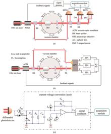
ObjectiveDue to the excellent detection performance, levitated optomechanical systems have become intriguing in the field of precision measurement. The detection schemes of such systems mainly contain the balanced photodetector (BPD) and quadrant photodetector (QPD). The BPD has a current differential structure that can eliminate common-mode DC signals, which results in extra low noise. However, the BPD scheme has the disadvantage of complicated detection systems because one BPD usually measures the particle displacement in one direction. In contrast, a QPD can simultaneously detect displacements in three directions, which effectively simplifies the detection system. Usually, QPDs amplify not only the AC photocurrent generated by the fluctuations of the incident optical power, which mainly arise from the displacements to be measured, but also the DC photocurrent corresponding to the average incident optical power. As a consequence, QPDs always show worse noise performance than BPDs. Therefore, this work proposes a QPD scheme, which reduces the electrical noise of a QPD through electrical filtering and achieves a common-mode rejection ratio (CMRR) as high as possible, and the response coefficients of the four quadrants are calibrated. The QPD is a promising alternative scheme to the BPD, which has high detection sensitivity and is beneficial to the miniaturization of levitated optomechanical systems.MethodsThis work proposes a QPD scheme by building the noise model in levitated optomechanical systems, according to which the proportions of electrical noise, optical shot noise, and relative intensity noise (RIN) can be obtained. A current filter circuit is built with an operational amplifier, and the DC and AC components of the photocurrent are separated without any influence on the junction capacitance of the QPD sensor. As a result, the AC transimpedance gain is free from the limitation of the DC component, and meanwhile, the electrical noise is reduced. The converted voltage signal from the AC component is used to demodulate the three-axis displacement information of the particle, and that converted from the DC component is used to indicate the position of the incident light on the QPD. Moreover, a QPD sensor with high saturated optical power is used to suppress the shot noise to the maximum extent. In addition, the bias voltage of the QPD sensor is adjusted to reduce the junction capacitance differences between the four quadrants, and the feedback resistance of each quadrant is calibrated through the connection of an adjustable potentiometer in series with a high-precision fixed resistance resistor. Consequently, the response coefficients of four quadrants are unified, and the CMRR of the detector is improved to a large degree.Results and DiscussionsAttributed to the calibration of the response coefficients, the junction capacitance difference between QPD quadrants is less than 1%, the circuit gain difference is less than 0.04%, and the phase difference is less than 0.02° (Fig. 4). The CMRR and noise performance of the QPD are tested in a levitated optomechanical system and are compared with those of a commercial BPD which meets the requirements of such a system with superior noise performance. The results show that the power spectral density (PSD) of the electrical noise of the QPD is -129.4 dBV2/Hz with a circuit gain of 105 and reaches the same level as that of the commercial BPD (Tables 1 and 2). The CMRR of QPD is greater than 45 dB (50-250 kHz), which is better than that of the commercial BPD [Fig. 5(b)]. When the incident optical power is in the range of 1-40 mW, the noise performance of the QPD is only limited by shot noise (Fig. 6, Table 2). Overall, compared with the commercial BPD, the QPD proposed in this work can better suppress RIN and has higher saturated optical power to effectively limit the influence of shot noise. Therefore, the detection performance of the proposed QPD can meet the requirements of levitated optomechanical systems.ConclusionsAn active current filtering scheme with operational amplifiers is designed in this work to improve the detection performance of the QPD-based levitated optomechanical system. A 105 single-stage transimpedance gain is achieved so that the electrical noise is optimized. The response coefficients of four quadrants are calibrated so that the CMRR is improved, which is greater than 45 dB in the frequency range of 50-250 kHz. When the incident optical power is in the range of 1-40 mW, the noise performance of the QPD is only limited by shot noise. The QPD scheme has been successfully applied for extremely weak force sensing in levitated optomechanical systems, which lays the foundation for the high-performance, miniaturized detection system. In the future, the delay introduced by the acoustic-optic modulator can be compensated with a calibration module, so as to further improve the common-mode rejection performance of the QPD scheme.
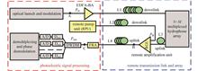
ObjectiveBottom-mounted and all-optical transmitted interferometric fiber-optic hydrophone array systems have the advantages of underwater uncharged and high reliability and are widely used in subsea oil exploration, marine acoustic exploration, and other fields. However, with an increase in the remote transmission distance, the phase noise of the system increases sharply due to the nonlinear effect of the fiber and high optical losses, which limit the detection performance. In optical communication, the schemes of remote pumped optical amplification (ROPA) and fiber Raman amplification (FRA), combined with large effective area and low-loss optical fibers, are used in long-distance unrepeated transmission systems, and good noise index and low bit error rate have been achieved. However, because optical-fiber hydrophone systems are based on a coherent detection scheme with high sensitivity, phase noise is a critical factor for the performance evaluation. Thus, the actual performance cannot be determined by only the noise index. However, only a few analyses and experimental studies on the phase noise characteristics of fiber hydrophone systems with remote pumped amplification and new-type fiber transmission structures have been reported. In this study, we developed a phase noise model based on a remote all-optical transmission and amplification structure for optical-fiber hydrophone systems with a hybrid time-division multiplexing (TDM) and wavelength-division multiplexing (WDM) array scheme. System parameters, such as the transmission link and remote gain position, were optimized through the model, which effectively reduced the system noise. The proposed noise model and optimization method can be applied to unrepeated fiber-optic hydrophone systems as they greatly improve the all-optical transmission distance and remote detection performance.MethodsBased on the structure of a remote-transmitted and amplified hydrophone system with a dedicated pump path scheme (Fig. 1), we developed a phase noise model of the remote amplification. First, the cascaded noise index of the hybrid optical amplification is calculated by comprehensively considering system parameters, such as the loss of the fiber hydrophone array, loss of the round-trip transmission link, remote pump power, and gain coefficient of the unit pump light. Second, the noise index is correlated with the beat intensity noise induced by the cascade amplification spontaneous emission noise at the receiver of the hydrophone system. Finally, combined with the phase-demodulation conversion coefficient, the TDM sampling aliasing, and other factors, the optical intensity beat noise is converted into a demodulated phase noise, and an equivalent phase noise model of remote optical amplification is obtained. Fig. 2 shows the simulation results of the phase noise associated with each stage of the amplifiers and the total noise of the remote amplification. The ROPA and FRA are the main noise sources in the remote system, and the huge transmission link loss combined with the insufficient input optical power of the remote pumped unit (RGU) are the key factors limiting the system's performance.Results and DiscussionsBased on the noise model, transmission-link-induced noise was simulated and optimized (Fig. 3) using a hybrid transmission scheme, which uses a large-effective-area and low-loss fiber (Type G.654) for the pump and signal-light transmission in the optical-fiber hydrophone downlink and an ultra-low-loss optical fiber (Type ULL-G.652) for signal-light transmission in the uplink. Also, in an experimental system with a 100-km transmission and a 4-WDM×8-TDM array scheme, the measured loss of the pump light is reduced by 2.1 dB (Fig. 4) compared with that of the traditional single-mode optical-fiber link (Type G.652), and Raman scattering of the pump light is also effectively reduced (Fig. 5). Then, the phase noise of the short system (Fig. 7) and the complete noise of the 100-km system (Fig. 6) were measured, and the phase noises independently induced by the remote amplification were obtained (Tab. 1). The results show that, with the combination of the G.654 and ULL-G.652 transmission links, the remote amplification noise can be reduced by 4.3 dB compared with that of the conventional G.652 link, reaching a low noise level of -98.1 dB@1 kHz. This reveals the effectiveness of the phase noise model (Tab. 1). Furthermore, the model was applied to a 150-km transmission system to optimize the position of the RGU, and the simulated result (Fig. 8) shows an optimal position of 115 km with -93.7-dB noise. Based on this result, an experiment was conducted, and the result shows a remote-amplification-induced noise of -93.2 dB@1 kHz (Fig. 9), which is consistent with the simulation result.ConclusionsIn this study, we developed a phase noise model based on an all-optical transmitted and amplified optical-fiber hydrophone array system. By analyzing the noise sources and characteristics, we propose a hybrid transmission link using large-effective-area and low-loss optical fibers. Both theoretical and experimental results show that the remote-amplification-induced phase noise in a 100-km transmission and 4-WDM×8-TDM system can be reduced to a low noise level of about -98 dB@1 kHz, which is 4 dB-5 dB lower than that of the traditional single-mode fiber link, revealing that the proposed transmission structure can effectively improve the noise performance of hydrophone systems. The RGU position in a 150-km transmission system was also optimized using the model, and the measured noise of the remote amplification is low (-93.2 dB@1 kHz), which is consistent with the simulation results. The proposed noise model and optimization methods for all-optical transmission and amplification systems can be applied to the design, implementation, and performance evaluation of remotely interrogated optical-fiber hydrophone systems, which could provide a critical technical support for extending remote transmission distances and improving the detection performance of such systems.
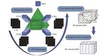
ObjectiveRecently, tomographic particle image velocimetry (TPIV) has been widely employed in the measurement of the flow field around a cylinder, turbulent boundary layer, flame field, and other flow fields since it is highly accurate, multi-point, three-dimensional, and instantaneous. The principle of TPIV is to reconstruct the three-dimensional scattering intensity distribution of particles in the flow field at the adjacent time and combine the three-dimensional cross-correlation algorithm to obtain its instantaneous flow field. 3D particle field reconstruction is the basis of TPIV and the premise of obtaining an accurate 3D flow field. Therefore, it is necessary to develop fast and high-precision 3D particle field reconstruction algorithms. The improvement of the reconstruction algorithm includes two aspects. The first is to improve the reconstruction accuracy, which is the similarity between the reconstructed particle field and the actual particle field, thus affecting the accuracy of the flow field. The second is to shorten the reconstruction time, since the reconstruction process needs to calculate the weight coefficient that is the intensity contribution value of spatial voxels to pixels, and iteration is adopted to update the intensity value of voxels. Thus, the reconstruction process often takes a lot of time, which is the biggest bottleneck in the TPIV application. Therefore, the calculation method of the weight coefficient plays an important role in reconstruction accuracy and reconstruction time.MethodsAccording to the imaging principle, the line of sight received by a pixel is a spatial volume, so only some of the voxels that contribute to the intensity of a certain pixel can be fully projected into the pixel. The partially projected voxels involve the weight coefficient calculation, which is related to the setting of the camera's internal and external parameters and the spatial volume. The traditional method often employs back projection to calculate the weight coefficient. However, due to a large number of divided spatial voxels and pixels, the order of the weight coefficient is usually large. Additionally, the back projection method not only needs to calculate each line of sight equation but also needs to calculate the number and volume of voxels intersected with the line of sight, thereby resulting in a huge amount of the weight matrix calculation. Therefore, reducing the calculation time of the weight matrix is the key to improving the reconstruction speed. In this paper, the area of voxels projected on the corresponding pixel is calculated as the weight coefficient, and a forward projection method (FPA) is proposed.Results and DiscussionsFirstly, a multi-view projection imaging simulation program based on the pinhole camera model for particles in 3D space is constructed, and artificial images are generated for analysis and verification. Secondly, FPA is combined with the current mainstream reconstruction algorithms (such as MART, MLOS+MART, and MLOS+SMART) to analyze reconstruction accuracy and time consumption. The results show that when FPA is employed for the reconstruction volume described in this paper, compared with the traditional backward method and the sub-grid method, the number of FPA weight matrix elements is reduced by about three and one orders of magnitude respectively, thus reducing calculation time and computer memory occupation. When the commonly experimental particle concentration pppp (particle per pixel) is 0.05, the reconstruction accuracy of this method combined with the current mainstream reconstruction algorithm will be higher than 0.8. In addition, based on the artificial images, the influence of the best camera acquisition angle and the experimental camera noise on the reconstruction results is analyzed, which proves that the reconstruction accuracy still meets the requirements of three-dimensional flow field reconstruction under the experimental noise conditions.ConclusionsA forward projection weight calculation method (FPA) based on single voxel is proposed in this paper. A particle projection imaging program in 3D space is constructed to verify the correctness of the proposed method. Taking the simulated imaging image as the reconstruction input, it is shown that the matrix elements of FPA combined with the MLOS algorithm can be reduced by about three and one orders of magnitude respectively compared with the traditional backward method and TSM, and the computing time can be reduced by 97% and 85% respectively, greatly reducing the computer memory consumption. Through similarity analysis, the average similarity of the weight matrix calculated by FPA and the traditional backward method is higher than 0.9974, which proves the reliability of FPA. Comparison between the reconstruction results of FPA and those of predecessors in the simplified two-dimensional plane shows that the reconstruction results of the FPA method combined with MART and MLOS+SMART only lose 0.02 reconstruction accuracy. Additionally, FPA together with MART and MLOS+SMART algorithms has good reconstruction results, and the reconstruction accuracy can reach more than 0.8 under the common experimental particle concentration (pppp = 0.05). By comparison, MLOS+FPA+MART has higher reconstruction accuracy and faster reconstruction speed, which is suitable for 3D flow field reconstruction. After the experimental noise is added to the imaging process, MLOS+FPA+MART is employed for reconstruction. The results show that the reconstruction accuracy after adding noise is still higher than 0.75, indicating that FPA has good robustness against noise. The analysis of the cross-symmetry camera layout in 3D space shows that the best acquisition angle of CCD2 in the cross-symmetry type is 15°–45° and 10°–40° respectively.
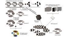
ObjectiveIn recent years, fringe projection profilometry (FPP) which can obtain dense three-dimensional (3D) shape information of measured scenes and digital image correlation (DIC) technique that can realize accurate deformation tracking have been combined to form a new method for simultaneously measuring 3D shape and deformation. However, in this method, FPP expects the measured surface's reflectivity to be uniform enough to ensure high accuracy of shape measurement, while DIC requires the measured surface to provide high-contrast texture information to ensure the accuracy of image matching and deformation calculation. These two techniques have different requirements for surface texture, and the contradiction is difficult to be solved in the traditional intensity space. Therefore, we propose a marker point texture hiding and extraction method in RGB color space, and the color difference of objects and marker points in the color space is used to perform a full-field linear transformation of color patterns. Finally, the contradiction in the texture requirements of FPP and DIC techniques is solved without the influence of color crosstalk and phase-shifting sinusoidal patterns, and accurate 3D shape and deformation measurement is achieved.MethodsThe basic idea of the method for achieving 3D shape and deformation measurement based on marker point hiding and extraction is to obtain hidden and extracted patterns of the marker points by using the color difference between the man-made color marker points and the object background, so that they can meet the requirements of the two techniques for the surface texture of the object. First, color marker points are made on the surface of the object according to the color of the measured object, and then gray-level structured light patterns are projected to the surface of the object. The deformed structured light patterns are collected by the color camera to obtain the texture pattern of the measured object. After that, according to the different intensity values of color marker points and backgrounds in three channels, the hiding coefficient and extraction coefficient are calculated, respectively. The high signal-to-noise ratio fringe pattern with uniform reflectivity is extracted by optimizing the hiding coefficient of the intensity values in the three channels. Meanwhile, the high contrast and robust marker point pattern is extracted by calculating the extraction coefficient of the intensity values in the three channels to get the high-contrast speckle pattern. The speckle pattern is used to complete the point matching of the reconstructed 3D shape, and the corresponding coordinate points are subtracted by using the point-to-point 3D coordinates to obtain the 3D deformation information. As a result, the marker point hiding and extraction method is suitable for complex dynamic scenes due to its point-to-point computing characteristics.Results and DiscussionsThe measurement results of the flat plate show that compared with two traditional measuring systems combining FPP with DIC, the marker point hiding and extraction method has a better performance in phase-unwrapping successful rate of the flat plate and in the sum of the square of subset intensity gradient of the texture map (Fig. 8 and Table 1). At the same time, compared with the traditional high-contrast black marker point in the intensity domain, the proposed method has higher shape measurement accuracy and equal deformation measuring accuracy (Fig. 9 and Fig. 10). Finally, the ideal fringe and texture patterns are obtained for the foam insole with complex particle surface under different pressures, and the complex 3D shape and deformation information of the foam insole is obtained, which verifies the superiority of this method in shape and deformation measurement in complex scenes (Fig. 11).ConclusionsA high-precision 3D shape and deformation measurement method based on marker point hiding and extraction is proposed, which can overcome the contradiction between FPP and DIC techniques on texture requirements. It demonstrates that the difference of color information between objects and markers in color space can solve problems difficult to be dealt with in traditional intensity space. At the same time, compared with traditional methods, the color marker points made by the proposed method have better noise resistance. In the whole process, there is no filtering operation or color crosstalk, and the linear transformation has no influence on the phase fringe, which can fundamentally solve the contradiction in texture requirements of FPP and DIC technologies and simultaneously complete the high-precision 3D shape and deformation measurement of complex structures. The proposed method is expected to be applied to strain stress analysis of complex structures such as laminates, honeycombs, and mold shells, and meet the requirements of complex detection in applications such as collision testing and fracture testing.
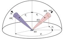
ObjectiveThe reflected light field information of a rough surface includes the reflected light angle and intensity, which can be used to retrieve the reflection and morphology characteristics of the surface. Therefore, accurate measurement of the reflected light field has high research value and practical applications in the fields of target detection and recognition, in-orbit radiation calibration, material property analysis, optical device stray light analysis, etc. Presently, the traditional "scanning" method uses a mechanical mechanism to achieve point-by-point scanning measurement of the spatial reflected light field information of the target sample; however, there are problems such as slow measurement efficiency, numerous measurement error links, and poor repeatability. Furthermore, given the influence of incident light wavelength and energy fluctuation on the measured data during the scanning process, the weight gradually increases with increasing time, which may lead to distortion of full-space BRDF fusion information. In contrast, the emerging "photographic" measurement method based on optical imaging techniques only measures the reflected light field in a small angle range. In this study, to overcome the low efficiency of the "scanning" reflected light field measurement system and the small measuring angle range of the "photographic" reflected light field measurement system, a rough surface reflected light field measurement method based on ultrawide-angle imaging is proposed. This method realizes the measurement of multidirectional angle reflected light field information over a large angle range, enriches measurement means of rough surface reflected light fields and is suitable for measuring optical reflection characteristics and damage of material surface. Here, the simulation and reconstruction provide a research basis and technical support.MethodsBased on the principle of reflected light field measurement, this paper first determined the overall structure of the reflected light field measurement system, which comprises a light source, sample plate to be measured, a hemispherical reflecting ball screen, and a refractive reflecting ultrawide-angle imaging optical system. Next, the catadioptric ultrawide-angle imaging optical system was optimized and the best resolution angle in the optical system's field of view was simulated and analyzed. Subsequently, a calibration method for the reflected light field measurement system was studied to realize off-axis spatial position calibration and light field intensity calibration. Finally, the reflected light field measurement results were simulated and analyzed using a Labsphere Permaflect-80 diffuse reflector, WhiteOptics-DF60 diffuse reflector, and American ACA specular aluminum plate, proving the feasibility of the proposed surface reflected light field measurement method.Results and DiscussionsThe best resolution angle of the designed reflected light field measurement system is 2° in the range of 0°-54° zenith angle and 15° in the range of 0°-360° azimuth angle (Fig. 9). The coordinate distribution of the feature points after calibration was obtained using the off-axis spatial position mapping relationship (Fig. 11); the relative error of light field measurement increases with increasing zenith angle. The maximum relative error in the range of the measuring field of view is 4.12% at the zenith angle of 54° and azimuth angle of 255°. The maximum average relative error is 2.06% and the average relative error is less than 1% within the range of 0°-36° zenith angle (Fig. 14). The measurement results were obtained using the Labsphere Permaflect-80 diffuse reflective plate, WhiteOptics-DF60 diffuse reflective plate, and ACA specular aluminum plate of the United States under conditions of uniform illumination using a 550-nm incident beam with a zenith angle of 40° and azimuth angle of 270°(Fig.16). The results show that the surface of specular aluminum material with rough surfaces have strong specular reflection characteristics, which is consistent with the reflection characteristics of the material itself (Fig.17).ConclusionsBased on the principle of ultrawide-angle imaging, a reflective light field measurement system has been successfully designed here that achieves a best angle resolution of 15° in the azimuth range of 0°–360° and a best angle resolution of 2° in the zenith range of 0°-54°. After calibration, the maximum average relative error of the circumference under each zenith angle is 2.06%. These results support that the "photographic" method of measuring a reflected light field can also be used to measure a reflected light field in a large angle range using a reasonable optical system design.
ObjectiveCorrosion has a great impact on the strength and durability of steel materials (such as rebar and steel plate). Research reveals the absorption resonance of some iron oxides produced during steel material corrosion with terahertz (THz) electromagnetic waves. Moreover, THz waves can penetrate common coating materials. Therefore, THz spectroscopy has application potential in non-destructive testing of the early corrosion of steel materials. To investigate the optical parameters of the corrosion products of steel materials and identify the characteristics of the products, we measured the THz transmission signals of different kinds of corrosion product samples and the main component crystals Fe3O4, Fe2O3, and α-FeOOH in the samples with a THz time-domain spectroscopy (THz-TDS) system. The experimental results show that in the effective frequency range of 0-1.2 THz, the refractive indexes of the mixture samples of different corrosion products are in the range of 2.7-3.4, and those of the component crystals Fe3O4, Fe2O3,and α-FeOOH are 4.0, 2.7, and 2.2, respectively. The content of Fe3O4 in the corrosion product mixture has a substantial influence on the optical parameters, such as absorption coefficient and refractive index. Then, we built an ultra-wideband THz-TDS system based on the two-color field to further extend the effective THz measurement range to 0-10 THz. The results indicate that within 0-10 THz, no characteristic absorption peaks of Fe3O4 are observed. In contrast, the characteristic absorption peaks of Fe2O3 are located at 3.4 THz, 4.2 THz, 4.85 THz, and 5.8 THz, respectively, and those of α-FeOOH are located at 3.6 THz, 4.05 THz, 5 THz, and 5.45 THz, respectively. In addition, this THz method can identify the characteristics of Fe2O3 and α-FeOOH from the THz absorption spectra of the samples of different corrosion products. Suggesting that the occurrence of steel material corrosion can be determined according to the characteristic absorption peaks of Fe2O3 and α-FeOOH, the experimental results in this paper lay a foundation for the application of THz spectroscopy in non-destructive testing of steel material corrosion.MethodsFirst of all, we used a Terapulse 4000 instrument to determine the transmission signals of samples of different kinds of corrosion products and the main component crystals Fe3O4, Fe2O3, and α-FeOOH. Then, we built an ultra-wideband THz-TDS system to extend the effective THz measurement range to 0-10 THz. Afterwards, this ultra-wideband THz system was employed to identify the locations of the characteristic absorption peaks of Fe2O3 and α-FeOOH. Finally, samples of different corrosion products were measured to identify the characteristics of Fe2O3 and α-FeOOH in the mixtures.Results and discussionTo investigate the optical parameters of corrosion product samples, we measured samples of different kinds of corrosion products and the main component crystals Fe3O4, Fe2O3, and α-FeOOH (Figs. 2-4). The experimental results show that the refractive indexes of the samples of the corrosion product mixtures are in the range of 2.7-3.4, and those of the component crystals Fe3O4, Fe2O3, and α-FeOOH are 4.0, 2.7, and 2.2, respectively. The content of Fe3O4 in the corrosion product mixture has a great influence on the optical parameters. Using the ultra-wideband THz system, we identified the locations of the characteristic absorption peaks of Fe2O3 and α?FeOOH. The characteristic absorption peaks of Fe2O3 are located at 3.4 THz, 4.2 THz, 4.85 THz, and 5.8 THz, respectively, while those of α-FeOOH are located at 3.6 THz, 4.05 THz, 5 THz, and 5.45 THz, respectively (Fig. 5). Furthermore, the characteristic absorption peaks of the Fe2O3 and α-FeOOH in the mixture samples were detected (Fig. 6), demonstrating that the mixture state of corrosion products does not affect the identification of the characteristics of Fe2O3 and α-FeOOH by THz spectroscopy.ConclusionsWe mainly studied the optical parameters of corrosion products and locates the characteristic absorption peaks of Fe2O3 and α?FeOOH. Since the components of the mixture samples of different corrosion products have different relative contents, the refractive indexes of the samples are in the range of 2.7-3.4. Moreover, the content of Fe3O4 has a great influence on the optical parameters of corrosion product mixtures. An ultra-wideband THz-TDS system based on the two-color field was built to extend the effective THz measurement range to 0-10 THz. The experimental results reveal that in the range of 0-10 THz, Fe3O4 has no characteristic absorption peaks; the characteristic absorption peaks of Fe2O3 are located at 3.4 THz, 4.2 THz, 4.85 THz, and 5.8 THz, respectively, and those of α?FeOOH are located at 3.6 THz, 4.05 THz, 5 THz, and 5.45 THz, respectively. The ultra-wideband THz waves can identify the characteristic absorption peaks of the Fe2O3 and α?FeOOH in the corrosion product mixtures. The characteristic absorption peaks of the two corrosion products Fe2O3 and α?FeOOH can be used as identification marks to determine the occurrence of corrosion. The experimental results in this paper lay a foundation for the application of THz spectroscopy to the non-destructive testing of the early corrosion of steel materials.
ObjectiveFor an aero-engine in operation, the pressure distribution of the exhaust jet flow field is the main parameter of flow characteristics and temperature field. Therefore, the accurate measurement of the exhaust jet flow field pressure of the aero-engine is of great significance to study the state of the aero-engine in operation. As traditional speed and pressure measurement tools, sensors such as pitot tubes fail to be directly applied to high-temperature and high-speed complex flow fields such as combustion due to their shortcomings of destructive flow fields, single point measurement, and low temporal and spatial resolutions. With the development of visual measurement and image processing technologies, optical measurement methods have been gradually applied to measure the physical parameters of the flow fields. As a typical optical diagnosis method, the pressure field reconstruction method based on particle image velocimetry (PIV) is only applicable to the pressure field reconstruction of incompressible fluid. As a flow field visualization measurement technology, the schlieren method has the characteristics of a large measurement range, fast response speed, and simple test equipment. It is an effective method for real-time measurement of flow field parameters. By applying the schlieren method to reconstruct the pressure field of the jet flow field of the aero-engine, the real non-contact measurement can be realized, and the accuracy of measurement can be improved.MethodsThis paper proposes a method of reconstructing the pressure field distribution of high-speed airflow by using the schlieren method to decouple the velocity and density fields, so as to realize the real-time measurement and reconstruction of the density field, velocity field, and pressure field of the high-speed airflow. First, the relationship between the brightness of schlieren images and the light shift is calibrated by using the calibrated schlieren method. After obtaining the calibration curve, the light shift can be obtained according to the light and dark changes in the schlieren images, and then the density distribution of the flow field will be indirectly obtained. Meanwhile, the velocity distribution can be obtained by using an optical flow velocimetry algorithm through the schlieren images of continuous frames. Finally, the static and dynamic pressure distributions of the flow field can be obtained through a numerical calculation by using the obtained velocity and density information, and then the total pressure distribution can be obtained.Results and DiscussionsThe density field (Fig. 11) and velocity field (Fig. 13) of the micro vortex jet wake field are reconstructed by the schlieren method, and the density field of the micro vortex jet wake field is reconstructed by using the obtained density and velocity information. In order to verify the feasibility and accuracy of the experimental method, the measured pressure at five points near the nozzle is selected and compared with the reconstructed pressure field (Fig. 18). The results show that the two results are close within the error range, and the maximum error is not more than 5%. The following factors are considered to determine error sources: when the density field of the flow field is measured, the model of the flow field is regarded as axisymmetric, and there is a certain error; when the pressure gradient distribution is calculated, the numerical calculation method is used, which has some errors; since the measurement time of pitot tubes and schlieren velocity-density field coupling reconstruction method is different, there will be some errors in the measurement results although the interval time is short. However, these errors are within the allowable range of measurement. Therefore, the reconstruction method of the high-speed airflow pressure field by using the schlieren method to decouple the velocity and density fields is feasible.ConclusionsIn this paper, the schlieren optical flow method is used to synchronously reconstruct the density and velocity fields of the axisymmetric flow field, which not only overcomes the shortcomings of the traditional single point measurement of pressure sensors, contact measurement, poor spatial and temporal resolutions but also compensates for the disadvantages of the PIV-based pressure field reconstruction technology. The technology requires the distribution of tracer particles and can only reconstruct the pressure field of incompressible fluid. Therefore, the proposed method is effective in accurately reconstructing the pressure distribution of high-speed flow fields, and it can extend the application scope of the schlieren method in the quantitative measurement of flow fields.
ObjectiveThere are two primary three-dimensional (3D) measurement error sources of structural light based on the phase shift method: phase shift error and nonlinear error. With the development of a digital projector, the computer can produce standard sinusoidal stripes to eliminate the phase shift error. However, the nonlinear error of the projector and camera will cause the stripe to lose particular sinusoidal properties, affecting the measurement accuracy and effect. To reduce the nonlinear error of the system, global scholars have put forward various solutions, among which the binary stripe method is the most widely studied. The binary stripe is not affected by nonlinearity because it has only two gray values. The projection speed can be significantly improved by a digital projector projecting 1-bit binary stripes. In the study of many binary stripes, the binary coded stripe method uses multiple binary stripes to generate a sinusoidal stripe, which avoids defocusing projection, effectively reduces the nonlinear effect of the system, and improves measurement accuracy and projection efficiency. Based on the binary coded stripe method, this paper proposes a method of reusing weighted binary coded stripes, which significantly reduces the number of binary stripes weighted with a sinusoidal stripe and further improves the projection efficiency.MethodsThis paper proposes a method of reusing weighted binary coded stripes. The binary coded stripe method samples the gray value of sinusoidal stripes uniformly to obtain the discrete decimal gray values of a sinusoidal stripe. The gray values are then processed by binary coding, and all of the code words with the same level of binary code words are combined to generate binary stripes. After sequential projection by a digital projector, the collected stripe images are weighted in binary to generate a sinusoidal stripe modulated by object depth information. In the implementation process of binary coded stripes, a certain number of repeated binary stripes will appear under a specific gray-value sampling number. After comparison, 12 gray values are uniformly sampled within a sinusoidal period, and the binary coding generates binary stripes. After unique processing, the same binary stripes only need to be projected once, and repeated weighting is performed in the calculation process. As a result, only four binary stripes are required to generate a sinusoidal stripe. Finally, the method is combined with the three-step phase shift technique. The complementary gray code method is also used to carry out the phase unwrapping, which can realize an efficient 3D measurement with 20 binary stripes in the state of constant focus.Results and DiscussionsThis paper uses the proposed method, three-step phase shift method, and the four-step phase shift method to measure different objects and carry out comparison experiments of different gray values, and the comparison experiment with the traditional methods aims to verify the superiority of the method of reusing weighted binary coded stripes. In the first experiment, through the measurement of a standard sphere, the average distance difference between local point cloud data obtained by different gray values and fitted standard sphere is small. The average distance obtained by the three-step phase shift optimization method is 0.0153 mm, and that by the four-step phase shift optimization method is 0.0107 mm (Fig. 6 and Table 3). As shown in Fig. 7, the actual item is measured, and the reconstructed results are comparable, which verifies that the proposed method of reusing weighted binary coded stripes can still maintain high accuracy and measurement impact after reducing the number of projections. In the comparison experiment with the traditional methods, sinusoidal fitting is carried out on the sinusoidal stripe obtained by the traditional methods and the proposed method. The root-mean-square error (RMSE) of the sinusoidal fitting is 3.6082 and 3.3125, and the sum of squared errors (SSE) is 3529.3 and 3028.4 (Fig. 8 and Table 4). Linear fitting is performed on the measurement results of the high-precision plane. The RMSE is 0.0415 and 0.0388 mm, respectively, and the SSE is 0.4804 and 0.4493 mm (Fig. 9 and Table 5). As demonstrated in Fig. 10 and Table 6, after measuring the standard sphere, the average distance between the local point cloud and the fitted standard sphere is reduced by 72.3% when compared with that by the traditional three-step phase shift method. For the measurement of the plaster head, whose surface depth varies greatly, the traditional three-step and four-step phase shift methods have strip-like systematic errors due to the nonlinear effects of the system. However, the surface reconstruction effect of the proposed method is better (Fig. 11).ConclusionsThis paper proposes a method of reusing weighted binary coded stripes. A better sampling scheme is designed by further studying the principle of the binary coded stripe method. After the unique processing of binary coding and binary stripes, the method of reusing weighted binary coded stripes generates sinusoidal stripes to reduce the actual projection number of binary stripes. In order to generate a sinusoidal stripe, eight weighted binary stripes are reduced to four binary stripes. As a result, only 20 binary stripes are required to complete the 3D measurement by the three-step phase shift method and the complementary gray code phase unwrapping method. The results of comparison experiments show that the proposed method will not reduce the measurement accuracy and effect while significantly reducing the projection number by the binary coded stripe method. Compared with the traditional phase shift method, the proposed method can significantly reduce the nonlinear effect of the system and further improve the projection rate of the DLP projector. In conclusion, the proposed method effectively reduces the projection number required by the binary coded stripe method and provides technical support for high-speed 3D measurement based on phase shift stripe analysis.
ObjectiveIn the high-precision-long-stroke manufacturing system, precise servo control of a motor determines the machining accuracy during manufacturing. Moreover, the value of the motor subposition is an important signal in the motor feedback control system, which determines the control precision of the linear motor servo system. Therefore, analyzing the position measurement algorithm for a high-precision-long-stroke linear electric motor is crucial. Currently, the linear electromotor measurement based on a digital image is mostly a short-stroke measurement and cannot achieve long-stroke precision measurement. However, with the continuous improvement of precision manufacturing requirements, the need for the accurate measurement of the displacement of long-stroke linear electric motor becomes extremely urgent. Moreover, unlike the two-frame image measurement system in short-stroke measurement, long-stroke measurement comprises a multi-frame image measurement system. The number of frames increases as the measurement distance increases, resulting in problems related to error accumulation. The cumulative measurement error is the most important factor that affects the measurement accuracy of rectilinear distance displacement. Hence, to address the issue of error accumulation owing to the displacement superposition of multiple frames during the measurement of the linear electromotor subposition, an error reduction algorithm based on machine vision with a threshold transform reference map was proposed herein.MethodsIn this study, the phase correlation algorithm is used to obtain the whole pixel offset between two frames rapidly, and the corresponding distance of the registration image is translated to decrease the displacement deviation between the registration image and reference frame to <1 pixel. The gray gradient algorithm is used to measure the subpixel displacement of the translated image in a small range. To improve the measurement accuracy and range of adjacent frames, then, the reference map is set, and the displacement images at different moments are registered to obtain the displacement value at specific moments. When the displacement between the registration map and reference map exceeds the maximum measured displacement between two frames, the transformation threshold is set to dynamically adjust the reference map. Based on the number of threshold transformations, the dynamic–real-time position is obtained using displacement superposition. Compared with the method of stacking adjacent frame displacements to obtain long-stroke displacement values, the proposed method can effectively reduce the displacement stacking time and cumulative error.Results and DiscussionsFirst, a one-dimensional image measurement system is designed based on the one-dimensional rigid body translation of the linear motor, and one-dimensional target images are generated and optimized to improve the accuracy of the measurement system, as shown in Figs. (1) and (3). The measurement range of the adjacent frame image measurement algorithm is optimized, and the measuring distance of displacement between two frames is extended, which lays a foundation for reducing the cumulative error. As shown in Fig. (6), the measurement range of the improved algorithm increases from 1 pixel to 189.54 pixel. Finally, the cumulative error reduction approach for a self-adjusting reference graph is proposed, which can reduce the cumulative error by ensuring high-resolution feedback from all positions through the changes in the reference graph, as seen in Fig. (7). The feasibility of the proposed method is verified via the experimental data in Figs. (10), (11), and (12). Fig. (11) verifies the feasibility of the proposed method, and demonstrates that its measurement accuracy is higher than the other methods. Fig. (12) verifies the robustness of the proposed method, which maintains a high level of measurement accuracy under low illumination conditions.ConclusionsIn this study, by improving the measurement accuracy of adjacent frames and decreasing the cumulative error, the long-stroke measurement of linear electromotor displacement with high precision is realized. First, image registration is divided into two parts: whole pixel translation and subpixel high-precision measurement. The accuracy and range of the algorithm in adjacent frame displacement image measurements are improved via step calculation. Then, to reduce the cumulative error in the displacement measurement process of long-stroke electromotor subunits, a threshold transform reference graph is added to reduce the cumulative times of displacement. The feasibility and effectiveness of the proposed method were verified via simulation and platform experiments. Experimental results show that compared with the traditional algorithm, the proposed method can effectively reduce the cumulative error by >80% and exhibit better cumulative error reduction under different illumination conditions. Therefore, the algorithm proposed herein can effectively reduce the cumulative error in the long-stroke measurement, which is conducive to the realization of high-precision measurement of the long-stroke linear electromotor displacement.
ObjectiveThe development of multi-core processors has greatly relieved the pressure of data processing. However, the capacity requirement for data transmission and exchange is still a challenge. Multi-dimensional multiplexing technologies are explored to meet the growing bandwidth requirements and provide a promising solution to address such a challenge. Among these technologies, mode division multiplexing in which each guided mode acts as an independent data channel has attracted much attention. Silicon-based optical mode switches are indispensable for reconfigurable on-chip mode division multiplexing. Previously, these switches have been demonstrated by a Y-junction combined with a multimode interference coupler and phase shifters, Y-junction couplers combined with 2×2 multimode interference couplers, and microrings. Although these devices can have good performance, sustained power consumption is required to maintain the switch states, which means they are volatile. In addition, due to the high refractive index contrast of the silicon-on-insulator platform, a strong polarization dependence would be formed. Thus, non-volatile polarization-insensitive silicon-based optical mode switches are highly desired. Owing to their outstanding properties, phase change materials are considered attractive candidate materials for realizing non-volatile integrated optical devices. To the best of our knowledge, non-volatile polarization-insensitive silicon-based optical mode switches employing phase change materials are never discussed before. Therefore, we wish to propose, design, and analyze a non-volatile polarization-insensitive silicon-based 1×2 optical mode switch using phase-change materials.MethodsThe proposed non-volatile polarization-insensitive silicon-based 1×2 optical mode switch using phase-change materials is composed of a polarization beam splitter, a polarization beam combiner, two directional couplers with phase-change materials operating in the TE0 and TM0 modes, a polarization-insensitive silicon waveguide crossing, and two-mode converter operating in the TE0 and TM0 modes. The proposed polarization beam splitter/combiner is based on a triple-waveguide coupler comprising two silicon waveguides on both sides and a Si-Si3N4 hybrid waveguide in the middle. By optimizing the structural parameters in the coupling region, a low-insertion-loss, and high-polarization-extinction-ratio polarization beam splitter/combiner can be obtained. For the two directional couplers with phase-change materials, a tapered silicon waveguide and a Si-Ge2Sb2Te5-ITO hybrid waveguide are employed to form the coupling region. The finite difference time domain method and particle swarm optimization algorithm are adopted to optimize the coupling region to obtain low insertion loss and excellent crosstalk. Similarly, the two-mode converters are based on counter-tapered couplers. With an aim at achieving high conversion efficiency in a wide wavelength range, the corresponding coupling regions are optimized through the finite difference time domain method and particle swarm optimization algorithm. The proposed polarization-insensitive silicon waveguide crossing consists of two orthogonal multimode waveguides in which the input and output tapers are mirror-symmetrical. The finite difference time domain method and particle swarm optimization algorithm are employed to optimize these tapers and finally realize low insertion loss and excellent crosstalk. As a result, a non-volatile polarization-insensitive silicon-based 1×2 optical mode switch with good performance can be achieved by tuning the phase state of phase-change materials.Results and DiscussionsThe functionality of the designed non-volatile polarization-insensitive silicon-based 1×2 optical mode switch is executed well (Fig. 13). When Ge2Sb2Te5 is in the amorphous state, the input TE0 and TM0 modes are transformed into TE1 and TM1 modes and emerge from the port output2. The input TE0 and TM0 modes will propagate forward and come out from port output1, if Ge2Sb2Te5 is in the crystalline state. When the designed device is operating in TE polarization, the crosstalk is less than -13.12 dB and the insertion loss is smaller than 1.37 dB within a bandwidth from 1535 nm to 1569 nm (Fig. 14). For TM polarization, within a bandwidth from 1535 nm to 1569 nm, the designed device exhibits a crosstalk of lower than -17.39 dB and an insertion loss of smaller than 1.61 dB. The corresponding fabrication tolerance is also discussed (Fig. 16). The waveguide width variation ΔW and the variation of Ge2Sb2Te5 thickness Δh exert great influence on the crosstalk and insertion loss of the designed device. Thus, the waveguide width and Ge2Sb2Te5 thickness should be precisely controlled. Ge2Sb2Se4Te1 can be employed to improve the crosstalk and reduce insertion loss further (Table 5).ConclusionsWe propose a non-volatile polarization-insensitive silicon-based 1×2 optical mode switch using phase-change materials. The proposed optical mode switch consists of a polarization beam splitter, a polarization beam combiner, two directional couplers with phase-change materials operating in the TE0 and TM0 modes, a polarization-insensitive silicon waveguide crossing, and two-mode converter operating in the TE0 and TM0 modes. The polarization-insensitive mode switching behavior is realized by adjusting the phase state of phase-change materials. The finite difference time domain method and particle swarm optimization algorithm are employed to design and analyze the presented device in detail. For the designed non-volatile polarization-insensitive silicon-based 1×2 optical mode switch using Ge2Sb2Te5, when the TE0 mode is input, the insertion loss is lower than 1.37 dB and the crosstalk is less than -13.12 dB within a bandwidth from 1535 nm to 1569 nm. As the TM0 mode is input, the insertion loss is smaller than 1.61 dB and the crosstalk is lower than -17.39 dB within a bandwidth from 1535 nm to 1569 nm. The results can provide references for optimizing the design of non-volatile polarization-insensitive optical mode switches.
ObjectiveWith the continuously shrinking lithography process nodes, new materials, and technologies are constantly introduced, which exerts different effects on the mark in the lithography machine alignment system. Therefore, improving the robustness of alignment marks is crucial for high-precision alignment. It takes extensive time and cost to verify the robustness of alignment marks based on experimental methods. The industry tends to adopt simulation experiments to improve research efficiency and economy. The theory of alignment mark simulation can be divided into scalar diffraction theory and vector diffraction theory. For alignment marks with small periods or complex structures, the rigorous coupled wave method in vector diffraction theory has good computational accuracy and speed. For the alignment mark simulation with complex structures, a robustness analysis method of alignment marks is proposed by combining the rigorous coupled wave method and the layered approximation method. The robustness of marks is analyzed by this method, and the lithography strategy of improving the process adaptability of the mark is clarified with the analysis results. The proposed method and the given process adaptability strategy show theoretical significance and application value for the alignment mark design and alignment accuracy of scanners.MethodsFor the ideal mark with the standard surface, a vector diffraction simulation model can be built by the rigorous coupled wave method. For alignment marks with sidewall deformation due to process influence, it is difficult to directly establish the surface function, as the surface is non-standard anymore. Therefore, a robust analysis method of alignment marks is proposed by combining the rigorous coupled wave method and the layered approximation method to meet the requirements. The alignment mark with sidewall deformation is divided into multiple layers with equal thickness. When the number of layers is large enough, each layer can be approximated as a rectangular structure. The alignment mark with complex structure can be replaced by a whole composed of multiple rectangular structures. The rectangular structure in each layer is analyzed according to the rectangular grating method. Then the Maxwell equations and boundary conditions of each layer and region are combined. Finally, the diffraction efficiency of the alignment mark with complex structure is calculated. Wafer quality (WQ), signal-to-noise ratio (SNR), and alignment error are three important factors affecting measurement accuracy, which are employed as evaluation functions to study the robustness of alignment marks.Results and DiscussionsWith WQ and SNR as the evaluation functions, the effects of the changes in groove depth, groove width, film thickness, and sidewall symmetry deformation on mark robustness are studied. The changes in groove depth, groove width, and film thickness cause the WQ and SNR to change approximately and periodically. The period is positively correlated with the measured optical wavelength. Under different wavelengths, the WQ and SNR show different peaks and valleys along with these parameter changes (Figs. 4-7). Therefore, the problem that these changes affect WQ and SNR can be solved by increasing the number of measurement wavelengths of the alignment system and selecting the signal channel with WQ and SNR as the measurement signal to improve the process adaptability of the alignment system. Symmetrical sidewall deformation shows little impact on the WQ and SNR of the mark, making it unnecessary to take targeted process adaptation strategies (Figs. 11-14). With the alignment error as the evaluation function, the robustness of the sidewall asymmetric deformation mark is studied. The diffraction efficiency of positive and negative order measurement signals of this mark is different, indicating that the alignment error is introduced (Table 2). With an aim to reduce the alignment error, on one hand, the asymmetric deformation is minimized through process optimization. On the other hand, the correct alignment position in the presence of deformation is obtained by solving the weights under multiple wavelengths. Finally, the correctness of the model is verified by the VirtualLab commercial software, and the marks are set up on the scanner for experimental testing. The simulation results are consistent with the experimental results, thus verifying the effectiveness and accuracy of the proposed method.ConclusionsIn this study, a robustness analysis method of alignment marks is proposed by combining the rigorous coupled wave method and the layered approximation method based on the simulation requirements of alignment marks for complex structures. The simulation model is built by this method. This paper analyzes the effects of groove depth, groove width, film thickness, and sidewall deformation on mark robustness. The changes in groove depth, groove width, and film thickness cause the WQ and SNR to change approximately and periodically. Additionally, the period is positively correlated with the measured optical wavelength. Under different wavelengths, the WQ and SNR show different peaks and valleys along with these parameter changes. Symmetrical sidewall deformation shows little impact on the WQ and SNR of the mark, whereas the mark deformation of asymmetric deformation introduces alignment error. The lithography strategy of improving the process adaptability of the mark is clarified with the analysis results. With the assistance of VirtualLab commercial software and the experimental platform, the validity and accuracy of the analysis method are verified. The research results in this paper show theoretical significance and application value for the alignment mark design and the alignment accuracy of scanners.
ObjectiveAs the revolution of new-generation information technology continues to advance around the world, the data traffic of the Internet is growing exponentially, and the demand for network bandwidth in various fields is increasing. The optical communication system, the core of networks, should continuously improve the frequency spectrum efficiency and the transmission capacity to meet the demands of future development. Hence, it faces great challenges. Silicon-based photonic integration technology has been developing rapidly due to its advantages of high integration, low costs, large bandwidth, and compatibility with CMOS technology. It is widely applied in optical fiber communication, optical sensing, optical modulation, quantum communication, optical neural networks, and other fields. The tunable silicon photonic filter is one of the most important components and plays a vital role in the wavelength division multiplexing (WDM) system of optical fiber communication. Optical filters include the Mach-Zenhnder interferometer (MZI), microring resonator (MRR), Bragg-gratings, arrayed waveguide grating (AWG), echelle diffraction grating (EDG), and MRR-assisted MZI (MRR-MZI). However, these filters have limitations in the size of devices, power consumption, flexibility, and adjustable range. Therefore, a tunable filter based on SOI material is proposed. The bandwidth and center wavelength of the filter can be tuned by the cascading of two filter units of the double-ring-assisted MZI, which guarantees that the filter output has a good shape factor and a flat passband.MethodsThe tunable filter of the cascaded double-ring-assisted MZI based on SOI material proposed in this paper is composed of two cascaded MRR-MZI filters. The spectral response of the tunable filter is the intersection of the transmission spectrum response of two double-ring-assisted MZI filters, and its bandwidth is determined by the overlapping region of the transmission spectrum response of the two units. Therefore, on the premise that the bandwidth and center wavelength of the filter can be adjusted, the output with a good shape factor and a flat passband is guaranteed. In design, the transmission function of the filter is calculated by the transmission matrix method, and the mathematical model of the filter structure is built by MATLAB. The appropriate range of the self-coupling coefficient between microring and MZI arm can be found when the stopband extinction ratios (SER), passband loss (PL), shape factor, and bandwidth tuning range of the filter output are used as the performance criteria. At the same time, MATLAB is employed to analyze the phase of the microring and obtain the appropriate phase to ensure that the output performance of the filter meets the design requirements. Considering the influence of loss and dispersion on the performance of the filter, we leverage the optical simulation software RSoft and the finite-difference time-domain (FDTD) method to simulate the performance of the component. The structural parameters of the microring are determined according to the self-coupling coefficient obtained by mathematical analysis. The effective refractive index of the microring is changed to simulate the phase control of the microring and achieve the bandwidth and center wavelength tuning of the filter, which is realized by changes in the temperature of the microring.Results and DiscussionsThe bandwidth of the cascaded double-ring-assisted MZI filter proposed in this paper can be tuned by simultaneous changes in the phase of the microring in the second unit filter (Fig. 11). As the effective refractive index of the microring increases, the 3 dB bandwidth of the filter changes from 5 nm to 1.5 nm, and the passband loss is between 0.73 dB and 0.88 dB, which meets the needs of optical fiber communication. The center wavelength of the filter can be tuned from 1548.05 nm to 1559.6 nm (Fig. 12) when the phase of the four microrings of the cascaded double-ring-assisted MZI filter is simultaneously changed, and the phase change in the big ring keeps twice as much as that in the small ring. During the center wavelength tuning, the shape factor changes from 0.78 to 0.60, and the 3 dB bandwidth changes from 5.0 nm to 4.6 nm, both of which remain unchanged.ConclusionsWe propose a tunable filter with a large bandwidth tuning range of the cascaded double-ring-assisted MZI filter. The system transmission function of the filter is derived by the transmission matrix method, and the theoretical analysis and performance simulation optimization are carried out. The simulation results show that the SER of the filter is greater than 20 dB, and the PL is less than 1 dB; the size of the device is 60 μm×87 μm. When the thermal-optical effect changes the refractive index of the microring resonator, the center wavelength can move in the whole free spectral range, and the output bandwidth can be tuned between 1.5 nm and 5 nm, which meets the requirements of different wavelength signal screening. The filter has the advantages of small size, wide bandwidth adjustment range, and low loss and can be widely applied in optical switching and optical signal processing.
ObjectiveStimulated Brillouin scattering (SBS) is an important topic in the field of laser-drive inertial confinement fusion (ICF). SBS can reduce the laser-target energy coupling efficiency, spoil implosion symmetry, and degrade target gain. The full-aperture stimulated Brillouin backscattering energy fraction diagnosis systems on the main laser fusion devices do not measure the spatial distribution of stimulated Brillouin backscattering signals, which simplifies the diagnosis system but loses the detailed features of stimulated Brillouin backscattering signals. An angle-resolved full-aperture backscattering diagnosis system is developed for the Shenguang-Ⅱ Upgrade (SG-ⅡU) facility to study the SBS process in the integration experiment of the double-cone ignition (DCI) scheme. The evaluation reveals that the angular resolution of the system is about ±2 °, and the diagnostic accuracy of energy fraction is ±15%.MethodsThe design of the system is guided by the temporal characteristics of the backward reflection signals on the SG-ⅡU facility. It is found that both SBS signals from the target and the third harmonic reflected light from the triple-frequency-conversion crystal (called laser signals in this work) propagate along the same direction but with a fixed time delay dependent on the geometry of the final optical assembly. The level of laser signals is proportional to the incident laser energy and is stable so that it can be used as a reference to infer the SBS energy fraction. An optical fiber array is designed to collect the angle-resolved signals reflected from the servo mirror of the SG-Ⅱ U facility. Then, the signals are split into two beams and recorded with two intensified charge-coupled devices (ICCD) separately. The time delay between the two ICCDs is determined by that between SBS signals and laser signals. To make sure the ICCDs record accurate signal energy and verify the timing and intensity ratio between the SBS signals and laser signals, the temporal characteristics of the ICCDs gating process are tested, and the total signals are also recorded with a streak camera coupled with a spectrometer. Assuming that the level of laser signals is known, the SBS level can be inferred.Results and DiscussionsIn this experiment, the related experiments under a laser focusing distance of 100 μm, 125 μm, and 150 μm from the crown are carried out to improve the laser-target energy coupling efficiency. Fig. 5(b) is the schematic diagram when the laser focusing distance is 100 μm. The distribution of stimulated Brillouin backscattering energy fraction under different laser focusing distances is investigated experimentally, and the related diagnostic results are shown in Fig. 7. For the cone target, when the laser focusing distance increases from 100 μm to 150 μm, the distribution of stimulated Brillouin backscattering energy fraction changes significantly. It can be seen from Fig. 5 (b) that for the cone target, when the laser focusing position is different, the local incident angle of the laser relative to the target surface varies, which causes the change in the laser-target energy coupling efficiency and the change in the plasma state during the laser loading process. Eventually, the distribution of stimulated Brillouin backscattering energy fraction also changes. For the diagnosis system in this paper, the main error sources are ICCD gain fluctuation, ICCD trigger jitter, ICCD gating characteristics, and data calculation errors. These factors are related to the specific experimental conditions and experimental settings. The comprehensive evaluation shows that the diagnostic accuracy of this diagnosis system is ±15%.ConclusionsThe SG-Ⅱ U facility is the main laser device for the research on the DCI scheme research at present. The first stage of the DCI scheme, quasi-isentropic compression, is completed by the 8-channel nanosecond beams. The laser plasma interaction process that occurs in this stage has a great influence on the compression effect. For the SG-Ⅱ U facility, a compact and portable stimulated Brillouin backscattering diagnosis system is developed on the basis of the diagnosis principle of relative measurement. The system can diagnose the distribution of stimulated Brillouin backscattering energy fraction with an angular resolution of about ±2°, and the diagnostic accuracy of energy fraction is ±15%. The preliminary diagnostic results show that the distribution of stimulated Brillouin backscattering energy fraction depends heavily on the focal location of the laser pulse on the target surface. The research provides reliable experimental results for the further study of SBS in the DCI scheme.
ObjectiveWith the development of the new energy vehicle industry, laser welding has been widely used in the manufacturing of power batteries for its fast welding speed, small heat-affected zones, and high degree of automation. During laser welding, the welding depth fluctuates because of the involved process parameters and impact factors, which produce defects such as insufficient welding depth and burn through. In order to avoid these defects, online monitoring of the laser welding depth is necessary to achieve quality monitoring. The indirect methods based on the various signals such as optical radiation, visual image, and acoustic wave in the process zone are easily affected by the welding process and cannot ensure high accuracy of the welding depth measurement. A laser welding depth monitoring method based on optical coherence tomography (OCT) directly measures the depth of the keyhole in the molten pool under deep-penetration welding conditions. This method is based on low coherence interferometry and aligns the measuring beam with the processing beam, which has the advantages of high measurement accuracy and strong anti-interference ability. The dynamic changes in the keyhole lead to the scattered distribution of the raw OCT data, and the post-processing of the raw OCT data is required to reveal the welding depth. The percentile filter is confirmed to be viable to process the raw OCT data. The accuracy of the welding depth extraction by using this method is easily affected by the noise of raw OCT data, and filter parameters are needed to adapt to different welding conditions. In order to solve the aforementioned problems, an OCT welding depth extraction method based on local outlier factor (LOF) and maximum filter is proposed in this paper. This is done by first detecting the noise points of raw OCT data using LOF and then applying the maximum filter to the cleaned OCT data.MethodsFirstly, this paper builds a laser welding depth measurement system based on SD-OCT and measures the keyhole depth under deep-penetration welding conditions. A longitudinal cross section of the weld seam is obtained to extract the actual welding depth. Then, the percentile filter is applied to the raw OCT data to extract the welding depth. In order to evaluate the accuracy of the welding depth extraction, the average error is introduced by considering the difference between the welding depth extracted from OCT data and the actual weld depth extracted from the longitudinal cross section. Next, the proposed method is applied to the raw OCT data to extract the welding depth. The noise points of the raw OCT data are first detected by LOF and removed from the raw OCT data. The welding depth is then extracted by the maximum filter. The proposed method is compared with the percentile filter in terms of the average error. Finally, in order to verify the repeatability of the proposed method, multiple welds with the same process parameters are performed.Results and DiscussionsA laser welding depth measurement system based on SD-OCT is established, and during the welding process, the raw OCT data are obtained (Fig. 4). Firstly, the percentile filter is applied to the raw OCT data to extract the welding depth. An average error of less than 5% can be achieved with a percentile between 92 and 98 and a window length greater than 200. Next, in order to further improve the accuracy of welding depth extraction, the proposed method is applied to the raw OCT data to extract the welding depth. The noise points of the raw OCT data are first detected by LOF, and the maximum filter is then used to extract the welding depth (Fig. 12). Furthermore, the comparison in average error between the proposed method and the percentile filter is conducted. The average error is 3.0% in the proposed method and 4.4% in the percentile filter (Fig. 13). Finally, multiple welds with the same process parameters are performed, and the proposed method is applied to extract the welding depth. The average errors are 3.0%, 3.8%, and 3.4%, respectively. Compared with the percentile filter, the accuracy of the welding depth extraction is improved by 32%, 22%, and 24%, respectively (Table 1). Therefore, it can be concluded that an average error of less than 4% can be achieved by the proposed method, and the accuracy of the welding depth extraction improves by up to 32% compared with the percentile filter.ConclusionsIn this paper, an OCT welding depth extraction method based on LOF and maximum filter is proposed. This is done by first detecting the noise points of the raw OCT data using LOF and then applying the maximum filter to the cleaned OCT data to extract the welding depth. By comparing the welding depth extracted from OCT data with the actual welding depth extracted from the longitudinal cross section, the average error of the proposed method is less than 4%, and the accuracy of the welding depth extraction improves by up to 32% compared with the percentile filter. The proposed method can well improve the accuracy of the welding depth extraction and is more applicable. The laser welding depth monitoring method based on OCT can achieve high measurement accuracy in continuous monitoring and provide quality assurance in industrial production. Further, it will be developed to realize the welding depth control for laser welding.
ObjectiveLasers for the waveband of 3-5 μm are important in the recognition and detection of gas molecules, free space optical communication, and different frequency generation of terahertz (THz). The typical pollutants and greenhouse gases such as H2S, SO2, CO2, and CO have strong absorption baseband in the waveband of 3-5 μm, so the development of lasers in this waveband is necessary.MethodsIn order to cover the waveband of 3-5 μm, the wavebands of 4.0 μm and 4.6 μm for two QCL gain chips are utilized as the gain medium. On the basis of the Littrow structure, the output beams of the two QCL gain chips are combined into one beam with a common aperture by using a low-pass and high-reflection beam splitter of 4.2 μm; the blazed grating of 300 lines/mm is used as the wavelength selector, the first-order diffraction light is fed back to the core of the gain chip to form an external cavity resonance, and the zero-order diffraction beam of the grating is used as the output light. By finely adjusting the position and the angle of the grating, the feedback light is returned to the core of the laser, and the laser wavelength is determined. The wavelength tuning gap of two QCL gain chips is used as the transition zone of the low-pass and high-reflection beam splitter, and the ultra-broad tuning range of the laser system can be achieved in the waveband of 3–5 μm.Results and DiscussionsUnder temperature of 25 °C and injection current of 303 mA, the laser system operates from 3779 nm to 4836 nm (including a wavelength tuning gap of 179 nm) (Fig. 5) with a rotation angle of 34.54°-46.50° for blazed grating tuning. The maximum output power is 14.12 mW (Fig. 7), and the SMSR is 20 dB (Fig. 6). In the wavelength range of 3779-4076 nm, the QCL gain chip of 4.0 μm operates with a threshold current of 188 mA and maximum output power of 5.24 mW (Fig. 7), while in the wavelength range of 4255-4836 nm, the QCL gain chip of 4.6 μm operates with a threshold current of 166 mA and maximum output power is 14.12 mW. In the waveband of 3-5 μm, there is almost no water absorption, and gas molecules such as H2S, SO2, CO2, and CO have strong absorption bands. In addition, the ability of the laser to have an ultra-broad wavelength tuning range makes it possible to simultaneously identify and detect these different molecules in the gas mixture.ConclusionsIn this paper, an ultra-broad tunable mid-infrared laser based on a beam combination of dual gain chips is designed. The laser system is built with QCL gain chips of 4.0 μm and 4.6 μm, a low-pass high-reflection beam splitter of 4.2 μm, and a blazed grating of 300 lines/mm. The experimental results show that the blazed grating angle for the QCL gain chip of 4.0 μm is 34.54°-37.69°, the maximum optical power is 5.24 mW, and the spectral tuning range is 297 nm. The blazed grating angle for the QCL gain chip of 4.6 μm is 39.67°-46.50°, the maximum optical power is 14.12 mW, and the spectral tuning range is 581 nm. The total tuning range of the laser is 3779-4836 nm (including a tuning gap of 179 nm), and the SMSR is 20 dB. The ultra-broad tunable mid-infrared laser can be used in gas molecule sensing, free space optical communication, and different frequency generation of THz in the waveband of 3-5 μm.
ObjectiveLight emitting diodes (LEDs) are widely used as backlight illumination sources in liquid crystal displays (LCDs). Narrow-band-emitting green phosphors have become a research focus due to their potential to extend the color gamut of LCDs, yielding high-definition/high-resolution displays with excellent picture quality. Current commercial LED backlight technologies make use of β-SiAlON∶Eu2+ narrow-band green phosphors [emission wavelength of λem=540 nm, full width at half maximum (FWHM) of 54 nm]and K2SiF6∶Mn4+ narrow-band red phosphors (λem =631 nm, FWHM of 3 nm) in conjunction with a 460-nm InGaN blue light chip. The peak emission level at 540 nm, and FWHM emission linewidth of around 54 nm of β-SiAlON∶Eu2+ green phosphors limit their application in wide color gamut displays. Therefore, there is a need to develop high-performance green phosphors with an emission peak at a wavelength of around 525 nm and with a narrower emission linewidth to address the shortcomings of existing commercial green phosphors.MethodsPotassium carbonate (K2CO3, mass fraction of 99.99%), sodium carbonate (Na2CO3, mass fraction of 99.99%), zinc oxide (ZnO, mass fraction of 99.99%), silicon dioxide (SiO2, mass fraction of 99.99%), boric acid (H3BO3, mass fraction of 99.99%), and manganese dioxide (MnO2, mass fraction of 99.99%) from Aladdincompanyare chosen as raw materials. A series of powder samples, K2-xNaxZnSiO4∶Mn2+(0≤x≤2), are synthesized by the conventional, high-temperature solid phase method. The physical structure of the materials is analyzed by an XRD-6100 powder diffractometer. Structural refinement of the XRD data of the samples is carried out by GSAS software. The morphology, particle size, and chemical composition of samples are analyzed with a JSM-7610FPlus field emission scanning electron microscope (SEM) and X-MaxN energy dispersive X-ray spectroscopy (EDS). The excitation spectra, emission spectra, and variable temperature spectra of samples are tested by an FLS920 steady-state/transient fluorescence spectrometer from Edinburgh Instruments Ltd., UK. Thermogravimetric tests are performed on the samples in an air atmosphere by a simultaneous thermogravimetric analyzer, i.e., STA449F3 thermogravimetric analyzer. The quantum efficiency of the samples is analyzed with a Hamamatsu C11347 absolute quantum efficiency tester.Results and DiscussionsThe crystal phase transition from the orthogonal phase K2ZnSiO4 to the monoclinic phase Na2ZnSiO4 is gradually achieved after K+ in the matrix is replaced with Na+. With the increase in the Na+ doping concentration, the main diffraction peaks of the K2-xNaxZn0.94SiO4∶Mn2+ (0≤x≤2) samples are continuously shifted to larger angles, which indicates that Na+ (with a smaller ionic radius) has been successfully doped into the K2ZnSiO4 material. As the Na+ doping concentration increases, the physical phase of the samples gradually transitions from K2ZnSiO4 to Na2ZnSiO4. This observation proves that Na+ gradually replaces the lattice position of K+ in the original material K2ZnSiO4 and forms a new phase (Fig. 1). The replacement of K+ with Na+ results in an increase in the average bond length of the central atom Zn-O, which leads to weakened crystal field strength around Mn2+ and a reduction in the degree of splitting [Eq. (1)]. As a result, it brings about higher energy emission wherein the wavelength emitted by Mn2+ becomes shorter. This is evidenced by the central wavelength of the emission spectrum from the sample blue-shifted from 578 nm to 517 nm, and the luminescence intensity of the sample is effectively increased (Fig. 4). The green phosphor K2-xNaxZn0.94SiO4∶0.06Mn2+ (x=2) is also subjected to variable temperature and thermogravimetric tests. At temperature of 150 ℃, the luminous intensity of the sample is 43% of that at room temperature. At temperature of 250 ℃, the residual mass ratio and the mass loss of the K2-xNaxZn0.94SiO4∶0.06Mn2+ (x=2) phosphor is 96.94% and of 3.06%, indicating that this phosphor has good thermal stability at operating temperatures typical of backlight LED devices (Fig. 7). Thus, the results demonstrate that a narrow-band, green phosphor with a narrower emission linewidth and shorter peak emission wavelength than the commercial β-SiAlON∶Eu2+ green phosphor is successfully prepared, achieving color tuning from deep yellow to green (Fig. 8).ConclusionsThis work demonstrates the synthesis of color-tunable K2-xNaxZn0.94SiO4∶0.06Mn2+ (0≤x≤2) phosphors with the high-temperature solid-phase method. The effect of the replacement of K+ with Na+ on the photoluminescence performance of K2-xNaxZn0.94SiO4∶0.06Mn2+ (0≤x≤2) phosphors is investigated. Under the excitation of blue light at 427 nm and 448 nm, the luminescence of samples gradually increases, and the main emission peak is blue-shifted as x increases. Ultimately, a narrow-band green phosphor with the main emission peak at 517 nm, the quantum yield of 29.4%, and an FWHM emission linewidth of 32 nm is obtained, which is narrower than that of the commercial green phosphor β-SiAlON∶Eu2+. This work presents a method and pathway to the development of new and novel narrow-band green light emitting phosphors for the next generation of backlight display technologies.
ObjectiveConfocal laser endomicroscopy (CLE) is an emerging imaging method with a cellular resolution for obtaining histopathological images of structure information on the mucosa in real time. CLE can significantly improve the detection rate of early tumors. Usually, the fluorescence from the tissue pre-stained with exogenous fluorescent dyes can be detected by the photodetector, which further generates corresponding electrical signals by the photoelectric effect and internal multiplication. Then, the electrical signal can be amplified to form CLE images after analog-to-digital conversion. Meanwhile, the output signal of the photodetector is influenced by the noise, which will further affect the quality of the final image. The noise in CLE mostly includes the shot noise introduced by the inherent fluctuation of obtained photons and the dark noise of detectors. So far, many researchers have mainly proposed CLE using mainly two types of photodetectors, such as avalanche photodiode (APD) and photomultiplier tube (PMT). Usually, APD has the advantage of high quantum efficiency and low cost. PMT has the advantage of high gain and low noise. Therefore, the advantages of the selected photodetectors are very different. At present, no researcher has thoroughly investigated the performance differences between APD and PMT. This paper presents a detailed comparative study of APD and PMT performance in CLE.MethodsBased on the different working principles of APD and PMT, the quantitative model for output signal-to-noise ratio (SNR) in CLE is obtained. The parameters include optical power, quantum efficiency and internal gain of the detector, system bandwidth, photocurrent, dark current, and amplifier noise. All parameters can be obtained from the user manual. Then, we implement a detector performance comparison test, and the light emitted from the LED of 525 nm is used to simulate the fluorescence of samples after passing through a neutral density filter and pinhole. This test not only provides a preliminary understanding of the differences between APD120A2 and PMTSS but also verifies the validity of the proposed model. Eventually, the most important CLE imaging experiment is carried out. For this experiment, a dual optical path CLE imaging system is established which allows simultaneous imaging with APD120A2 and PMTSS under the same optical system by using the beam splitter of 50∶50. The fluorescent samples for this experiment are fluorescein sodium solution, fluorescent beads with diameter of 13 μm, lens tissue (stained by sodium fluorescein), and Photinia serrulata leaves (stained by sodium fluorescein). Distribution of the number of pixels with different optical powers and image SNR is the quantitative evaluation index of the images in this experiment.Results and DiscussionsValidity of the detector output SNR model for CLE is verified by the detector performance comparison test. This test shows that the SNR of APD120A2 is 2.74 dB on average lower than that of PMTSS. The theoretical value of the model matches with the experimental results, and the correlation error is less than 4.8% (Fig. 5 and Fig. 6). In addition, there is an upper limit to increase the SNR of PMTSS by adding the internal gain of PMT. By imaging the fluorescein sodium solution, we find that due to fluorescence quenching and other factors, the image SNR difference between APD120A2 and PMTSS is 0.28 dB on average (Fig. 7), which is much smaller than the result in detector performance comparison test. The imaging results of other fluorescence samples indicate that the dark current of APD120A2 is higher than that of PMTSS, which affects the low light detection capability of APD120A2. When the average fluorescence optical power is less than 10 nW, the difference in image SNR between APD120A2-based CLE and PMTSS-based CLE increases with decreasing optical power. APD120A2-based CLE imaging performance is comparable to PMTSS-based CLE imaging performance when the average fluorescence optical power is greater than 10 nW. Under this condition, the difference of image SNR is less than 0.67 dB (Fig. 9). Thus, when the optical power is lower than 10 nW, APD120A2 is not recommended for CLE because of the higher dark noise.ConclusionsThis paper presents a detailed study to compare the influence of the selected differences in photodetector on the imaging performance of CLE systems. Firstly, a quantitative model for APD-based and PMT-based CLE SNR is proposed considering different parameters. Secondly, a comparison test for detector performance is carried out to verify the model, which aims to understand the characteristics of APD and PMT. In the end, a dual optical path CLE experimental system is built to evaluate the practical effects of APD120A2 and PMTSS in CLE. The experimental results show that the imaging performance of the APD120A2-based CLE is comparable to that of the PMTSS-based CLE when the average fluorescence optical power is higher than 10 nW. Therefore, in the design of the CLE, it is necessary to determine the detected optical power range for CLE. Selecting APD instead of PMT as the CLE photodetector can obtain more cost-effective imaging results. In the future, based on the SNR model in this paper, we will further improve the imaging quality of APD-based CLE systems by selecting APDs with lower noise factors and designing low-noise APD peripheral circuits. The research results can also provide guidance for selecting photodetectors in low-light detection applications.
ObjectiveThis paper proposes a novel asymmetric microstructure different from the existing light-trapping structures. By reducing the specular reflection, the microstructure can improve the stray light suppression performance at a small angle of incidence. The microstructure can be installed in the internal structure of the optical system to effectively reduce the mass and size of the optical system and improve the stray light suppression performance of hoodless optical systems.MethodsComparing the theoretical stray light suppression performance of microstructures with different angles between the front reflective surface and the baseline of the substrate surface, this paper designs asymmetric microstructures whose angle between the front and back reflective surfaces is 90° and angle β between the front reflective surface and the baseline of the substrate surface is smaller than 45°. To fabricate the asymmetrical microstructures, this paper also proposes a laser galvanometer processing system for tilting machining. Subsequently, the intensity distribution of the focused laser is obtained by drawing on the research on the action range of the focused light spot under different tilt angles and applying the phase recovery technique (Fig. 4). When the tilt angle of the laser is 60°, the intensity distribution of the focused light spot is in a shape similar to that of the microstructure shown in Fig. 3. Then, a new high-speed laser processing platform is designed and utilized to process the surface of aluminum alloy samples. The three-dimensional morphology of the processed sample surfaces is measured by confocal laser scanning microscopy (CLSM). The formation mechanism of the microstructure surface under different scanning velocities is preliminarily investigated, and the appropriate processing parameters are obtained. Furthermore, the specular reflection test experiment and the integrated simulation experiment are designed to evaluate the performance of the samples.Results and DiscussionsThe investigation of the surface morphology of the microstructures processed at different scanning velocities shows that when the processing scanning velocity is 1600 mm/s, the average angle between the front and back reflective surfaces of the microstructure is 93.5°, which is close to the designed angle of 90° shown in Fig. 6(d). In the specular reflection test experiment, the ability of the microstructure to suppress specular reflection is verified [Fig. 8(d)]. Then, in the integrated simulation experiment simulating the influence of off-axis collimated stray light on the optical system, the angle of incidence is set to 15°, and the illumination light source is 650 nm laser. The relative reflectivity of the microstructure surface is 10% that of the conventional anodized surface. Only visible light sources (520 nm and 650 nm) are used as test light sources in this paper, and the performance of the proposed microstructure in the infrared wavelength range will be tested in the follow-up research. In addition, the processing parameters will be further optimized, and the mechanism of tilting laser on the formation of the microstructure will be investigated to improve the manufacturing accuracy of the microstructure and thereby improve the stray light suppression performance of the microstructure surface.ConclusionsA novel microstructure with asymmetric characteristics is designed. In this microstructure, multiple reflective surfaces are periodically arranged on the substrate surface. The off-axis stray light is suppressed by increasing the reflection angle of the stray light and changing the reflection direction. The angle of incidence is set to 15°, and the illumination light source is 650 nm laser. The stray light suppression performance of the microstructure is 10 times higher than that of the conventional anodized surface, and its relative reflectivity is only 0.008%. No light-absorbing coating is added to the surface of the tested microstructure sample. It is believed that a microstructure surface with better performance can be obtained by adding a light-absorbing coating to the surface.
ObjectiveRecently, additive/subtractive hybrid manufacturing has arisen to harness the merits of both additive manufacturing and traditional subtractive manufacturing. In this study, a novel hybrid machine tool that combines selective laser melting (SLM) and high-speed dry milling is employed to produce 316L stainless steel widely used in modern industries to produce shells, values, pipes, feeders, wristwatches, connectors, etc. Sliding wear properties are important for 316L stainless steel products in certain applications because they may have a vital impact on the service life of these products. This study investigates the effects of SLM/milling-based additive/subtractive hybrid manufacturing processing parameters on the relative density, hardness, surface roughness, coefficient of friction (CoF), and wear rate of 316L stainless steel. In addition, it analyzes the mechanisms of dry sliding wear of 316L stainless steel produced by additive/subtractive hybrid manufacturing.MethodsGas-atomized 316L stainless steel powder is used as the feedstock (Fig. 1), and samples are produced by hybrid manufacturing with the hybrid machine tool (Fig. 2), which have varied laser power, scan speed, resultant laser energy density ranging from 112.5 J·mm-3 to 183.3 J·mm-3, and feed per tooth ranging from 0.02 mm to 0.08 mm. For analysis and comparison, other samples are produced by the SLM method with the same additive processing parameters as those in hybrid manufacturing. Cast 316L stainless steel samples are produced by a machining center with the same milling parameters as those in hybrid manufacturing. Then, the relative density of the samples with varied SLM processing parameters is tested through Archimedes' method. The hardness of the samples is tested by a microhardness tester. A 3D profiler is used to test the surface roughness. Defects in microstructures and the surface morphology of the samples are investigated under an optical microscope to relate the characteristics of the samples to the processing parameters. Dry sliding wear tests are performed at room temperature by counter balls of Si3N4 to obtain the CoF of the samples. The wear rate and wear track morphology are explored under the 3D profiler and a scanning electron microscope (SEM). The element composition of the worn surfaces is analyzed by energy-dispersive X-ray spectrometry (EDS).Results and DiscussionsThe relative density and hardness of the samples produced by SLM are in the ranges of 93.8%-99.2% (Fig. 4) and 232.3-283.6 HV0.2 (Fig. 6), respectively. For E=150 J·mm-3, the highest relative density and maximum hardness are obtained, and the number of pores and cracks in the microstructures is the smallest. Pores or cracks (Fig. 5) may result in a lower hardness value (Fig. 7). Defects, differences in re-melt times, and grain orientations-caused variables result in hardness tests. The grain size of the cast samples is much larger than that of the samples produced by SLM, and the hardness is about 208 HV0.2. The surface roughness after milling is much better than that after SLM (Table 4), and there is some debris on the surface caused by the dry milling process. With varied, the CoF and wear rate of the polished SLM samples are in the ranges of 0.93-1.03 and 5.02×10⁻⁸-7.51×10⁻⁸ mm3·mm-1, respectively, and they both obtain their minimum values when the highest density is obtained (Fig. 10). In the first 15 min of sliding, higher surface roughness causes a more significant fluctuation in CoF for the SLM samples. The total wear rate of the surface produced by hybrid manufacturing is lower than that of the surface produced by SLM, and it decreases as the feed per tooth declines. The milled surface of cast 316L stainless steel shows a slightly higher CoF, while with the same feed per tooth, it shows a slightly lower wear rate than that of SLM-manufactured 316L stainless steel. At the beginning of sliding, abrasive grooves occur on the processed surfaces, and other types of wear follow as the sliding goes on (Fig. 11). Abrasive wear and fractures that result in small craters are the elemental wear mechanisms on SLM-processed surface, while adhesive wear is mild. On surfaces processed by hybrid manufacturing, abrasive wear occurs near the edges of the wear track, while debris adhesion and surface flattening occur in the center of the wear track. On the milled surfaces of cast 316L stainless steel, abrasive wear and fractures govern material loss. Elastic deformation at the edges can be observed on the wear tracks of the milled surfaces, while on the SLM-processed surface, burrs are difficult to grow. After 30 min sliding, the main wear mechanisms for samples produced by SLM are abrasive wear and adhesive wear (Fig. 12). Pores in these samples play a vital role in material loss because they cause fractures during sliding, and they affect the CoF and wear rate (Fig. 13) in several ways. The cast 316L stainless steel shows similar wear mechanisms except that it exhibits more craters than the SLM-built 316L stainless steel, though no obvious pores are observed near the fractures. The processes of dry sliding in the air of 316L stainless steel, SLM-built and cast, are accompanied by prominent oxidation in places where adhesion occurs, which can be attributed to the severe plastic deformation of the adhered debris (Fig. 14).ConclusionsA hybrid process has an advantage over a sole additive process in manufacturing parts with sliding wear resistance. A surface manufactured in a hybrid manner is comparable to a milled surface of cast 316L stainless steel in sliding wear resistance despite the fact that there are differences in their sliding wear mechanisms. In additive/subtractive hybrid manufacturing, the additive process parameters affect the wear characteristics of 316L stainless steel by regulating the number of defects in the microstructures, and a decrease in defects in the microstructures suggests an improvement in the dry sliding wear resistance. By modifying the state of the initial surface of 316L stainless steel after the additive process, the subtractive process improves the sliding wear resistance at the early stage of sliding, and a decreasing feed per tooth can enhance the dry sliding wear resistance.
ObjectiveAs a photoelectric image sensor widely used in the field of aeronautics and astronautics, charge-coupled device (CCD) has attracted much attention due to its proton irradiation damage in the space environment. Performance degradation and function failure will be caused by irradiation damage when CCDs are applied to the orbiting satellite or the space imaging system. The irradiation damage effect of CCDs generally includes total ionizing dose, displacement effect, and single event effect. The total ionizing dose and displacement effect will cause permanent damage by influencing the semiconductor material in CCDs to induce oxide defects and interface defects. The single event effect will induce high charge density in the sensitive region of CCDs and disturb the output signal. The damage induced by the single event effect will be gradually recovered in the next signal transfer period. As an important factor causing CCD performance degradation in the space irradiation environment, proton irradiation damage is necessary to be studied, which is of significance to improve the reliability of CCD application in the space irradiation environment. We report the proton irradiation experiments of CCDs with different energy and fluence on proton cyclotrons. The degradation of CCD property parameters such as conversion gain, dark signal, and linear saturation output induced by proton irradiation is analyzed. We hope that our experiment and analysis can be helpful for designers to improve the reliability of CCD applications in space irradiation environments such as space exploration and satellite imaging.MethodsCCD proton irradiation experiments with proton energy of 60 MeV and 100 MeV are carried out on Xi'an 200 MeV Proton Application Facility (XiPAF). The irradiation fluence is 1×10¹⁰, 5×10¹⁰, and 1×1011 cm-2, respectively. All pins of the CCD are offline and unbiased during irradiation. The CCD model used in this experiment is ICX285AL. The pixel size is 6.45 μm×6.45 μm, and the total number of effective pixels is 1392×1024. Its advantages of low noise and high sensitivity meet the requirements of proton irradiation experiments. The CCD parameter test is carried out on the irradiation effect parameter measurement system of photoelectric image sensors based on European standard EMVA1288. The measurement system is composed of a measurement host computer, integrating sphere, sample carrier, and darkroom. The laboratory temperature before and after irradiation is about 25 °C. In this study, the gray value of the dark field image measured in the irradiation effect measurement system of photoelectric image sensors is used as the output signal of the sensor. The value of conversion gain is calculated by the curve of variance gray value and mean gray value, and the dark field image is used to analyze the change in dark signal spike before and after irradiation.Results and DiscussionsIn this study, experiments of proton irradiation of 60 MeV and 100 MeV on CCDs are carried out to analyze the experimental law of CCD performance degradation induced by proton irradiation. The CCD linear part slope of the photon transfer curve produces a certain extent of reduction because the output amplifier of CCDs can be damaged by proton irradiation, which indicates that the conversion gain of CCDs decreases along with the increase in the irradiation fluence (Fig. 3 and Fig. 4). The linear saturation output of CCDs also degrades after proton irradiation with different energy because proton irradiation produces a high concentration of oxide defects and interfacial trapped charge in the CCDs (Fig. 6). In addition, with the increase in irradiation fluence, both conversion gain and linear saturation output degrade to some extent, and proton irradiation with higher energy will induce more serious degradation of conversion gain and linear saturation output than that with lower energy (Fig. 5 and Fig. 6). The study of dark signal shows that the quantity of dark signal spike increases significantly after proton irradiation, and the density of dark signal spike increases with higher energy under irradiation (Fig. 7 and Fig. 8). The dark current of CCDs under proton irradiation raises with the increase in the irradiation fluence, which indicates that both the bulk dark current and surface dark current generated by proton irradiation cannot be ignored (Fig. 9). Furthermore, higher irradiation energy is accompanied by greater increase in dark current. The CCDs irradiated with protons produce ionizing energy loss (IEL) and non-ionizing energy loss (NIEL). The IEL and NIEL are used to evaluate proton irradiation damage of CCDs. Proton ionization damage and proton displacement damage are related to IEL and NIEL, respectively. Overall, the IEL and NIEL induced by proton irradiation of 60 MeV are greater than those induced by proton irradiation of 100 MeV.ConclusionsThe experiments of high energy proton irradiation of 60 MeV and 100 MeV on XiPAF are introduced in this study, and the experimental law of CCD performance degradation induced by proton irradiation is analyzed. The conversion gain, dark signal, and linear saturation output of CCDs degrade obviously, and the dark current significantly increases after proton irradiation. Under the same irradiation fluence, the degradation of conversion gain and linear saturation output induced by proton irradiation of 60 MeV is more serious than that by proton irradiation of 100 MeV, and more dark signal spikes and larger dark currents are produced. The degradation of the above parameters indicates that CCD performance will be seriously affected by proton irradiation. The results show that CCDs are very sensitive to the damage caused by proton irradiation as an image sensor working in the space environment, and the study provides a reference for the research on the damage mechanism of CCD high energy proton irradiation.
ObjectiveA tunable stabilized optoelectronic oscillator (OEO) based on stimulated Brillouin scattering (SBS) is proposed to solve the low stability problem of microwave signals output by the OEO. An OEO is affected by the characteristics of devices in the structure and the external environment, and the frequency and intensity of its output microwave signals have a certain degree of fluctuations, which influences its subsequent application. Therefore, it is important to improve the stability of microwave signals output by OEOs for improvement in OEO performance. For the OEO based on electric filters to achieve oscillation frequency selection, researchers have improved the frequency stability of output signals by effectively controlling devices such as intensity modulators and optical fibers or electric filters. However, the inclusion of an electrical filter in the structure limits the tunability and integrability of the OEO to some degree. Researchers have introduced the SBS effect into the OEO loop instead of the electrical filter to achieve the oscillation frequency selection so that the tunable range of OEO can be increased. However, the OEO structure usually confronts the problems of laser wavelength drift and DC bias drift, which affect the stability of the microwave signal output by OEO. Therefore, this study proposes a simple-structured OEO that can output a more stable microwave signal and achieve more integrated devices.MethodsA single light source is used to provide an optical carrier and pump light, and the phase modulator (PM) is used to modulate the phase of the optical carrier. It is worth mentioning that the RF signal initially loaded onto the PM comes from the white noise at the photodetector (PD), which is amplified by an electrical amplifier (EA) and fed back to the RF port of the PM to realize the phase modulation of the optical carrier. The Brillouin gain spectrum and Brillouin loss spectrum generated by the SBS effect of pump light in the dispersion-shifted fiber (DSF) break the amplitude balance of the phase modulation sidebands of the optical carrier, and the light wave is photoelectrically converted by the PD to obtain a microwave signal. Then, the microwave signal is fed back to the PM, and through continuous positive feedback, the OEO finally outputs a stable oscillating microwave signal. For higher stability of microwave signals, a tunable stabilized OEO based on SBS is designed. the SBS effect is used instead of an electrical filter to achieve frequency selection, and a single light source is used to provide the optical carrier and pump light, which simplifies the device structure. No other bias regulating devices are introduced into the structure to avoid the effect of DC bias drift, which makes the microwave signal output by the OEO more stable. The use of DSF as the SBS effect medium in the structure reduces the influence of the phase changes in the phase modulation sidebands of the optical carrier caused by the fiber dispersion effect.Results and DiscussionsA tunable OEO based on SBS is designed to raise the stability of its output microwave signal. The frequency of microwave signal output by the OEO with a laser wavelength of 1553 nm is 10.48 GHz (Fig. 6(a)), and the measured phase noise is -94 dBc/Hz@10 kHz. Through adjustment to the laser output wavelength, the OEO outputs a microwave signal tunable in the range of 10.13 GHz to 10.65 GHz (Fig. 6(b)), i.e., a tuning range of 520 MHz. At the resolution of 1 MHz, the frequency and intensity stability of the microwave signal output by the OEO is measured within 20 min. In addition, there is no drift in frequency (Fig. 7(a)), and the intensity fluctuation is 1.15 dB (Fig. 7(b)). Under the same conditions, when the optical carrier and pump light are provided by two independent light sources, the microwave signal output by the OEO has a frequency fluctuation of 82 MHz (Fig. 9(a)) and an intensity fluctuation of 1.69 dB (Fig. 9(b)). The experimental results show that compared with the OEO that uses two independent light sources to provide the optical carrier and pump light, the single-source OEO has a simple structure, and the intensity stability of its output microwave signal is improved by 0.54 dB, with its frequency measured without fluctuations at 1 MHz resolution.ConclusionsIn this paper, a tunable OEO based on SBS is proposed, which has the advantages of high frequency, high stability, low phase noise, and tunable output frequency. The output microwave signal frequency is tuned from 10.13 GHz to 10.65 GHz, i.e., a tuning range of 520 MHz, by changing the output wavelength of the tunable laser. The phase noise is measured at 10.48 GHz to be -94 dBc/Hz@10 kHz, and the output microwave signal reports no frequency drift in 20 min and a maximum power drift of 1.15 dB. The experimental results show that compared with the dual-source OEO, the single-source OEO has a simple structure and can output a more stable microwave signal. It is a better choice for obtaining a microwave signal with high frequency, low phase noise, and high stability.
ObjectiveRadar cross section (RCS) is an important physical quantity to measure the radar echo capability of the target. To reduce the RCS value of the target object is to achieve RCS reduction, which has important applications in the field of radar stealth. Terahertz (THz) waves refer to electromagnetic waves in the frequency range of 0.1-10 THz, which have broad application space in high-speed broadband communication, precision military radar, high-resolution imaging, and other fields. With the increasing complexity of the international situation and the rapid development of science and technology, RCS reduction in the THz band and its application in radar stealth has become a new research direction. Currently, there are two most effective and commonly used methods for RCS reduction in the THz band. The first one is to use a perfect absorber, which can absorb the incident THz waves to the surface and convert them into internal energy. The other is to use a metasurface to reshape the THz wave waveform in the space domain. The former has the disadvantages of narrow bandwidth and easy discovery by far-infrared detectors. The latter has become a hot research topic because of its simple structure, small size, and wide operating frequency band. In this paper, a coding metasurface with more degrees of freedom than the traditional metasurface is adopted. By combining it with a phase gradient metasurface, this paper proposes a coding phase gradient metasurface. Compared with the normal coding metasurface without phase gradient, it has a better RCS reduction effect. Moreover, the coding phase gradient metasurface has a wider working band. This is due to the introduction of a double Ω-shaped symmetrical structure at the top of the metasurface element. The metasurface will generate magnetic dipole resonance and electric dipole resonance in its interior, and the multiple resonance modes are conducive to broadening its working frequency band.MethodsFirst, according to the Pancharatnam-Berry (PB) geometric phase principle, a number of double Ω-shaped reflective metasurface elements with different phase responses are designed. The conditions they meet are as follows. For the vertically incident x- and y-polarized waves, the amplitudes of the co-polarized reflection are almost the same, and their co-polarized reflection phase difference is 180°. Second, based on the designed metasurface elements, the coding elements are designed. The so-called coding element is the introduction of phase gradient on the basis of the supercell. Third, a genetic algorithm is written using Matlab to optimize the arrangement, so that the energy distribution of diffuse reflection is more uniform, and a better RCS reduction effect is obtained. Then, according to the optimized arrangement, the coding elements 0 and 1 are arranged to obtain the coding phase gradient metasurface. Finally, CST Microwave Studio is used to simulate the far-field scattering of the coding phase gradient metasurface at different frequencies. The RCS reduction value relative to a metal plate of the same size is calculated. In addition, the influence of x- and y-polarized incidence angles on the performance of the coding phase gradient metasurface is also analyzed.Results and DiscussionsWhen the x- and y-polarized waves are incident vertically to the metasurface element, the co-polarization amplitudes are larger than 0.8 in the frequency range from 1 THz to 1.5 THz, and their phase differences are close to 180°, which satisfy the PB geometric phase principle (Fig. 2). Then, the phase gradient is introduced on the basis of supercells, and 1 bit coding elements 0 and 1 are designed (Fig. 4). The optimal arrangement M1 of the coding elements is achieved with the help of the genetic algorithm [Fig. 6(b)]. The coding phase gradient metasurface is obtained by arranging the coding elements according to M1. CST Microwave Studio is used to calculate the far-field scattering of the coding phase gradient metasurface at different frequency points under the normal incidence of x- and y-polarized waves. The result shows that the diffusely reflected scattering waves will be further reflected in the direction of the two symmetrical main lobes, and the far-field beams have both diffuse reflection and abnormal reflection characteristics (Fig. 9). In addition, the results show that the designed 1 bit coding phase gradient metasurface can achieve RCS reduction of more than 10 dB (Fig. 10) in a wide frequency range (0.87-1.725 THz) with a relative bandwidth of 65.9%. The RCS reduction in the frequency range of 0.9-1.4 THz and 1.6-1.7 THz both reaches over 15 dB with a maximum RCS reduction value of 31.26 dB. The RCS reduction effect of the coding phase gradient metasurface (composed of coding elements 0 and 1 arranged according to M1) is compared with that of the normal coding metasurface without phase gradient (composed of supercells 0 and 1 arranged according to M1), and it is found that the RCS reduction effect of the former is better. Finally, when the incident angles of x- and y-polarized waves are both gradually increased from 0° to 30°, the RCS reduction is more than 10 dB in the frequency bands of 0.9-1.5 THz and 0.9-1.7 THz (Fig. 11). It indicates that good RCS reduction effect can be achieved over a wide frequency range with a certain degree of angular stability.ConclusionsIn this paper, a coding phase gradient metasurface is proposed, which can reduce the RCS in the THz band. The results show that the designed 1 bit coding phase gradient metasurface can achieve RCS reduction of more than 10 dB in a wide frequency band from 0.87 THz to 1.725 THz, and the maximum reduction value reaches 31.26 dB. Finally, the influence of the incident angles of the x- and the y-polarized waves on the performance of the coding phase gradient metasurface is analyzed. It was found that its performance is stable in the range of 0° to 30°. The above results show that this kind of metasurface has potential application value in radar stealth and other aspects.
ObjectiveObtaining narrow-linewidth (high-Q-factor) plasmon resonances in metal nanostructures is of crucial importance for improving device performance, which is limited by the intrinsic Ohmic and radiative losses of metal nanostructures. Fano resonance based on the coupling between the subradiant "dark" and superradiant "bright" plasmon modes in metal nanostructures has generally been recognized as an efficient strategy to narrow the linewidths of plasmon resonances. For this reason, it has been widely utilized for improving the performance of nanodevices, such as nanolasers and nanosensors. Recently, the design and generation of multiple Fano resonances have also attracted extensive attention for the further improvement and expansion of the functionalities of metal nanostructures, which is still a challenge. Up to now, the "symmetry breaking" mechanism, the plasmon-waveguide coupling mechanism, and the complex plasmon-graphene nanostructures are three main schemes for exciting multiple high-order narrow-linewidth modes and further inducing the generation of multiple Fano resonances by coupling the high-order modes with the broad-linewidth plasmon modes. More recently, multiple Fano resonances have also been successfully and experimentally observed in simple spherical dielectric-metal core-shell resonators as a result of the near-field coupling among the multipolar sharp cavity plasmon modes and the broad sphere plasmon mode. In addition, the excitation efficiency (resonance intensity) of the multiple high-Q-factor cavity plasmon modes is also of great importance for applications in certain cases, but it has not been studied so far as well. Therefore, this paper systematically (theoretically and experimentally) studies the influences of the shape (spherical or ellipsoidal) and the integrity (with or without small openings at the sidewall equator) of the metal shell array on the excitation efficiency of the multiple high-Q-factor cavity plasmon modes.MethodsThe optical spectra (absorption, reflection, and transmission) and the near-field electromagnetic field distributions are calculated by the three-dimensional finite element simulation software COMSOL Multiphysics 5.4. To simplify the calculation, this paper sets the simulation domain to a cuboid composed of two separate quarters of the PS/Ag core-shell structures. The incident light is set to a plane wave with perpendicular incidence with respect to the array, and the perfect electric conductor boundary conditions and the perfect magnetic conductor boundary conditions are applied to the incident electric field direction and the incident magnetic field direction along the four sides of the simulation domain, respectively. Perfectly matched layers are applied to the upper and lower surfaces of the simulation domain to absorb reflected and transmitted light. The PS/Ag core-shell array is experimentally fabricated by employing the recently developed self-supporting technology. In brief, a monolayer of monodisperse PS spheres (the coefficient of variation is smaller than 2%) with a diameter of 994 nm is first self-assembled on the water/air interface by a modified Langmuir-Blodgett method. Subsequently, they are transferred onto a substrate with tens of micrometer-sized through-holes to form a self-supporting PS microsphere monolayer by exploiting the strong interparticle van der Waals interactions. Then, thin silver films with an identical thickness are successively deposited on the upper and lower half-surfaces of the self-supporting PS monolayer in the fashion of plasma sputtering. Remarkably, the existence of the small connections between adjacent PS microspheres results in the formation of six trumpet-shaped openings at the sidewall equator of the silver shell.Results and DiscussionsSpecifically, the absorption, reflection, and transmission spectra of the perfect spherical silver shell array are theoretically calculated. The results demonstrate that the electric-based cavity plasmon modes (TM2 and TM3) can be efficiently excited while the magnetic-based cavity plasmon mode (TE1) has low excitation efficiency (Fig. 1). In addition, the excitation efficiency of the TE1 cavity plasmon mode can be greatly promoted by either changing the shape of the silver shell from spherical to ellipsoidal or constructing six small openings at the sidewall equator of the spherical silver shell. This is further revealed by the changes in the shape and the enhancement of the electric field (Fig. 2 and Fig. 3). Especially, an optimal opening angle (about 20?) can be obtained to maximize the excitation efficiency of the TE1 cavity plasmon mode even for different silver thickness in the range of 30-70 nm (Fig. 3). Furthermore, the TM2, TE1, and TM3 cavity plasmon modes can be simultaneously efficiently excited in the non-perfect ellipsoidal silver shell array with six small openings (the opening angle is about 20?) at the sidewall equator (Fig. 4). Last but not least, the non-perfect ellipsoidal silver shell array with six small openings (the opening angle is about 20?) is successfully fabricated by applying the recently developed self-supporting technology. The measured transmission spectrum is in good agreement with the theoretical one, confirming the simultaneous high efficient excitation of the multiple high-Q-factor cavity plasmon modes (Fig. 5).ConclusionsThe shape and the integrity of the silver shells have a substantial influence on the excitation efficiency of the multiple high-Q-factor cavity plasmon modes. The theoretical results show that the electric-based cavity plasmon modes (TM2 and TM3) can be efficiently excited while the magnetic-based cavity plasmon mode (TE1) has low excitation efficiency in the perfect spherical silver shell array. The excitation efficiency of the TE1 mode can be significantly improved by engineering the silver shell from spherical to ellipsoidal or constructing six small openings at the sidewall equator of the spherical silver shell. In particular, an optimal opening angle (about 20?) is theoretically available to maximize the excitation efficiency of the TE1 mode. Further theoretical investigation reveals that the TM3, TM2, and TE1 modes can be efficiently excited in the non-perfect ellipsoidal silver shell array with an opening angle of about 20? simultaneously. In experiments, the non-perfect ellipsoidal silver shell array is successfully fabricated by employing self-supporting technology. The actual opening angle of the silver shells is precisely estimated to be about 20?, representing excellent agreement with the theoretical optimal value. As a result, the measured transmission spectrum is also in good agreement with its theoretical counterpart, directly confirming the simultaneous efficient excitation of the multiple cavity plasmon modes.
ObjectiveTunability is an important requirement for metasurface application. In recent years, adjustable materials have been gradually used in the composite design of metasurface structures to achieve multi-functional switching. However, most of the existing relevant studies still have some shortcomings. First, the adjustable material is usually embedded in the metal pattern, which undoubtedly increases the complexity and manufacturing difficulty of the structure. Second, commonly used adjustable materials such as vanadium dioxide and graphene require particularly sensitive temperature environments or feeding conditions, and the temperature and bias voltage should be considered in the design and application, which not only complicates the production process but also brings a certain degree of difficulty to the practical application. Third, most of the reported metasurfaces only discuss the insulating and metallic states of adjustable materials, which limits the diversity of functions. Photosensitive silicon is a kind of light-adjustable material, and its conductivity changes with the change in pump light energy. It has attracted wide attention because of its simple regulation mode. Moreover, photosensitive silicon can continuously adjust the conductivity to generate a variety of coding states, so as to expand its functions. In this paper, a reconfigurable metasurface based on a photosensitive silicon pattern is designed. The metasurface does not need to change the shape, size, or direction of the unit but uses the optical control to continuously adjust the conductivity of photosensitive silicon, so as to realize several functions in the terahertz band, such as linear-to-linear polarization conversion, linear-to-circular polarization conversion, broadband absorption, near-field imaging, and beam splitting, which makes the regulation mode of multifunctional terahertz devices more convenient.MethodsIn this study, the pattern of the unit structure is completely composed of photosensitive silicon, and the processing technology of silicon-based metasurface is very mature, which will greatly reduce the production difficulty. The conductivity of photosensitive silicon varies with the light energy pumped. When the light energy increases, the carrier concentration in the semiconductor also increases. By adjusting the conductivity of the two photosensitive silicon rings, five coding states can be obtained, so as to encode metasurfaces with different functions. In this paper, the polarization conversion and absorption function can be realized by using the resonance between the photosensitive silicon and the metal plate or between the double rings. The amplitude difference of different state units can be used for imaging, and the phase difference can be used for beam splitting.Results and DiscussionsThe designed metasurface can generate multiple coding states by continuously adjusting the conductivity of two photosensitive silicon rings (Table 1), so as to realize multifunctional switching in the terahertz band. When the conductivity of the large and small C-rings is 5.0×10⁵ S/m and 0 S/m, respectively, the designed metasurface is presented as a linear-to-linear polarization converter (Fig. 2), and the polarization conversion ratio (PCR) in the range of 2.10-3.15 THz is greater than 90%. When the conductivity of the large and small C-rings is changed to 0 S/m and 5.0×10⁵ S/m, respectively, the structure behaves as a linear-to-circular polarization converter (Fig. 4) in the range of 2.33-2.47 THz and 2.78-4.40 THz. When the conductivity of the large and small C-rings changes to 2.5×10⁵ S/m at the same time, the structure is transformed into an absorber (Fig. 7) with an absorption rate of more than 90% in the range of 2.40-4.60 THz. By encoding the cells with the conductivity of both large and small C-rings of 0 S/m and 2.5×10⁵ S/m, the structure achieves near-field imaging (Fig. 12) in the range of 2.80-3.00 THz. The cells with the conductivity of 5.0×10⁵ S/m and 0 S/m for the large and small C-rings and those with the conductivity of 0 S/m for the large and small C-rings are periodically coded, and this structure can realize two beam splitting (Fig. 14) and four beam splitting (Fig. 15) of the terahertz wave. The results show that the metasurface can be reconstructed by changing the external illumination conditions, and a variety of terahertz control functions can be obtained.ConclusionsIn this paper, the reconfigurable metasurface designed by the photosensitive silicon double C-rings structure realizes the switching of several functions, such as linear-to-linear polarization conversion, linear-to-circular polarization conversion, broadband absorption, near-field imaging, two beam splitting, and four beam splitting. Compared with the existing reports, the structure pattern designed in this paper is completely composed of photosensitive silicon, which greatly reduces the complexity of the pattern and the difficulty of device manufacturing. At the same time, this paper makes use of the continuously adjustable conductivity of photosensitive silicon to generate a variety of coding states, making the function of the metasurface more abundant. Compared with the single-function metasurface, it has greater advantages in integration and other aspects. In a word, the metasurface proposed in this paper is more flexible in switching functions and can realize a wider range of functions. It has excellent application prospects in terahertz modulation, stealth technology, communication system, and so on.
ObjectiveTerahertz wavefront manipulation, particularly flexible switching of terahertz wavefronts through programmable metasurface, has good prospects for application. Electricity, temperature, and light control are the most common programmable metasurface control methods available today. In order to directly modulate an electronically controlled metasurface, diodes loaded on both ends of a particular metal structure are typically powered through an external power supply. However, due to the structural characteristics of the diodes, it is difficult to reduce the cell area for terahertz wave modulation. Temperature-controlled metasurfaces use phase-change materials to change the metasurface's reaction to electromagnetic waves. However, precise control of the ambient temperature is required. In addition, the phase-change material takes time to alter states, which induces the terahertz wave's low modulation efficiency. Optically controlled metasurfaces can integrate photosensitive semiconductors into elements to control the amplitude and phase characteristics of metasurface units by changing the properties of photosensitive materials. However, existing metasurfaces lack accurate optical control of the individual elements, which makes it impossible to modify the wavefront of incident terahertz waves by encoding the elements according to digital metamaterials theory. In this paper, a 2 bit phase-encoded metasurface unit is realized by controlling the conductivity of the embedded photosensitive semiconductor in the top metal split ring of the cell through the encoding of the structural light source to simulate different C-shaped rings. Subsequently, by encoding the spatial distribution of structured light, the developed metasurface units are built into arrays to generate angularly adjustable anomalous reflections and vortex beams of different orders. A new optical control method is proposed here. It is combined with spatially encoded structured light and can efficiently solve the problems of the existing optical control metasurface's single function and high processing difficulty.MethodsIn this paper, a metal split ring construction with an embedded photosensitive germanium material is used to imitate the reaction of a C-shaped ring to terahertz radiation. By changing the electrical conductivity of the embedded photosensitive germanium material with the different encoding of structural light, it switches between the metallic and insulated states, thus changing the connection state of the metal split ring on the top layer of the metasurface. The metal split ring with different connection states can polarize the incident terahertz waves while adjusting their phases. In this paper, we realize a metasurface unit with 2 bit phase encoding by finding a suitable encoded structured light. In the next step, we combine the designed 2 bit phase encoded units with digital encoding metamaterial theory to form different metasurface arrays to achieve anomalous reflections at different angles and vortex beams of different orders, thus verifying the correctness of the metasurface cell design.Results and DiscussionsThe period of the optically controlled metasurface unit designed in this paper is 40 μm (Fig. 2). The 2 bit phase difference at 3.5 THz is achieved by changing the connection state of the metal split ring at the top of the metasurface with the different encoding of structured light. In this study, we digitally encode structured light and photosensitive materials in the form of least significant bit (LSB) (Fig. 3). Bit 0, Bit 1, Bit 2, and Bit 3 correspond to the codes 11000110, 00111000, 00011011, and 00001110 (Table. 1), respectively. The phases of Bit 0, Bit 1, Bit 2, and Bit 3 at 3.5 THz on the metasurface are 68.2°, 157.8°, 248.3°, and 337.8°, respectively. The amplitude of the cross-polarization of metasurface units is approximately the same while forming a 2 bit phase difference. The amplitudes of Bit 0, Bit 1, Bit 2, and Bit 3 at 3.5 THz are -0.91 dB, -1.196 dB, -0.91 dB, and -1.194 dB, respectively (Table. 2). In this paper, Bit 0 and Bit 2 are selected to form arrays with different lattice periods to achieve a double-beam splitting with beam splitting angles of 32°, 20°, and 15.3° (Fig. 6). Next, a single-beam anomalous reflection is achieved by selecting all bit units to form 8, 12, and 16 lattice metasurface arrays with reflection angles of 15.4°, 10.1°, and 7.4° (Fig. 7), respectively, and the angle decreases with increasing phase gradient encoding period. The vortex beam has a wide range of applications, including increasing system communication efficiency and capacity convenience. The 1st-order, 2nd-order, and 3rd-order vortex beams are realized by different spiral phase encoding methods (Fig. 8), and the beam center depressions are all more than 25 dB below the main flap, with good performance.ConclusionsIn this paper, a novel optically controlled metasurface method based on encoded structured light is presented. The combination of spatially encoded structured light and photosensitive semiconductors achieves independent amplitude phase tuning of the optically controlled metasurface unit. The problem of precise tuning of the optically controlled terahertz metasurface unit is solved. In this paper, the 2 bit phase encoded optically controlled terahertz metasurface is realized by combining the digital metamaterial theory. With the theory of digital metamaterials, anomalous reflections at different angles and vortex beams of different orders are achieved by different encoding methods, which realizes the flexible modulation of terahertz wavefront and enriches the application of optically controlled terahertz metasurfaces, and a new idea for developing optically controlled metasurfaces is provided.
ObjectiveWith the advantages of high flexibility, high security, and large communication bandwidths, vortex beams play an important role in many fields, such as quantum entanglement, spatial optical communications, particle manipulation, and optical microscopy. In optical communication applications, the orbital angular momentums (OAMs) of vortex beams can be used as a new encoding method for high-dimensional information encoding. This method can not only achieve mode-division multiplexing and scale the capacity of optical communications but also improve the channel capacity and spectral efficiency of optical communications. It thus provides a potential solution for future high-speed, high-capacity, and high-spectral-efficiency optical communication technologies. This study proposes an encoding method based on OAM and radial modes for composite vortex beams. It uses a 5-bit binary sequence to encode the light intensity distributions of 32 different composite vortex beams generated by the coaxial superposition of two vortex beams. The topological charge and radial index of the incident vortex beam are detected by the proposed gradually-changing-period gratings for decoding purposes. The research results of this study provide a theoretical basis for extending the applications of the OAM modes of vortex beams in the encoding and decoding field.MethodsTo generate large topological charges and make demodulation easier, this study proposes an optical communication method and system featuring the encoding of composite vortex beams with spaced OAM modes. Specifically, a Laguerre-Gaussian (LG) vortex beam with fixed OAM and radial modes is coaxially superposed with an LG vortex beam with four radial modes (p=0, 1, 2, 3) and eight equally spaced OAM modes (l=±3, ±5, ±7, ±9) to generate and further encode the light intensity distributions of 32 different composite vortex beams with a 5-bit binary sequence. Then, Eq. (3) is used to convert the 32 composite vortex beams into 32 single LG vortex beams, which will irradiate the proposed gradually-changing-period gratings in the x-axis and y-axis directions. The p and l of the single LG vortex beams can be successfully detected by leveraging the far-field diffraction patterns of the gratings and then be used to derive the composite vortex beams. In this way, the information can be decoded correctly.Results and DiscussionsThe light intensity distributions of the 32 composite vortex beams are shown in Fig. 1. The results reveal multi-ring patterns in the light intensity distributions. The radius of each ring increases as the OAM mode |l2| rises, and the number of patterns in each ring is |l2-l1|. In addition, the number of rings in the light intensity distributions increases with the radial mode p2, and the number of rings is p=max(p1, p2)+1. Figure 2 presents the encoding sequences for the composite vortex beams shown in Fig. 1. According to Fig. 2, the corresponding encoding sequences for the composite vortex beams LG02+LG03–LG06+LG3-9 are 00000-11111. Figure 3 illustrates the light intensity distributions of the 32 single LG vortex beams converted by Eq. (3) from the composite vortex beams shown in Fig. 1. In Fig. 3, the OAM value of a single LG vortex beam is the absolute value of the difference between the OAM values of the two superposed beams, and the radial mode of a single LG vortex beam is the maximum value of the radial modes of the two superposed beams. Figures 4(a) and 4(b) are the proposed gradually-changing-period gratings in the x-axis and y-axis directions, respectively. Figure 4 indicates that the period changes gradually in the x-axis and y-axis directions, respectively. A comparison between Figs. 5 and 7 suggests that when the beam passes through a gradually-changing-period grating, its adjacent far-field diffraction sub-pattern has dark nodal lines. The number of the nodal lines is related to the OAM value of the incident LG vortex beam and satisfies Eq. (6). Moreover, the direction of the nodal lines is determined by whether the OAM value of the incident LG vortex beam is positive or negative. Regarding the x-axis gradually-changing-period grating, the nodal lines of the diffraction pattern at the -1 diffraction order are from upper left to lower right while those of the diffraction pattern at the +1 diffraction order are from lower left to upper right when the lm of the incident vortex beam is positive. In the case of the y-axis gradually-changing-period grating, the nodal lines of the diffraction pattern at the -1 diffraction order are horizontal while those of the diffraction pattern at the +1 diffraction order are vertical when the lm of the incident vortex beam is positive. Figures 6 and 8 show the 32 far-field diffraction patterns produced after the 32 single LG vortex beams pass through the x-axis and y-axis gratings, respectively. The results suggest that the far-field diffraction patterns can be used to successfully detect the parameters of the single LG vortex beams for correct decoding without being affected by the increases in the OAM or radial modes.ConclusionsThis study derives the expression of the intensity of each composite vortex beam generated by the coaxial superposition of two LG vortex beams and uses a 5-bit binary sequence to encode the simulated light intensity distributions of 32 different composite vortex beams. The far-field diffraction patterns of the x-axis and y-axis gradually-changing-period gratings designed and proposed in this study can be used to successfully detect the parameters p and l of the single LG vortex beams. The results show that a multi-ring pattern can be observed in the light intensity distributions. The number of rings is p=max(p1, p2)+1, and the number of patterns in each ring is |l2-l1|. In addition, the proposed x-axis and y-axis gradually-changing-period gratings can be utilized to successfully detect the parameters of the incident beams for correct decoding without being affected by the radius of each ring or the number of rings in the light intensity distributions.
ObjectiveThe development of deep space exploration and interstellar flight technology imposes higher requirements on the performance of spacecraft, especially on the energy power system and wireless communication system. However, in the typical satellite orbit region in space, the environment is filled with huge numbers of high-energy particles, such as protons, electrons, and heavy ions, due to the strong impact of solar proton events, Van Allen radiation belts, and galactic cosmic rays. Consequently, spacecraft are always exposed to the threat of various radiation effects caused by high-energy radiation particles, resulting in storage errors, communication losses, attitude losses, and other problems. In serious cases, the flight mission may fail instantaneously. The high-power near-infrared laser produced by the high-power 975 nm GaAs-based quantum well (QW) laser diode (LD) has outstanding advantages, such as high directivity, great monochromaticity, high optical power density, and long transmission distance. For this reason, such QW LDs have become the optimal choice to achieve long-distance wireless energy transmission and wireless communication in the complex space environment. Nevertheless, their development is seriously hindered by the harsh space environment and radiation effects. Therefore, to address the urgent need for major strategies in the radiation field, this paper studies the degradation law and triggering mechanism of high-power semiconductor QW LDs in radiation environments.MethodsThe accelerator is investigated by ground simulated irradiation experiment and simulation calculation and analysis. Specifically, regarding the current typical spacecraft orbit, the accumulated 10 MeV proton equivalent displacement damage dose (DDD) is calculated under the condition that the spacecraft has been in orbit for 10 years, and its value is between 3×108 cm-2 and 3×1011 cm-2. Then, the 10 MeV proton irradiation experiment in vacuum at room temperature is carried out using the Beijing HI-13 tandem accelerator, and the optical power, volt-ampere characteristics, and spectral performance of the LDs are tested before and after irradiation. Furthermore, Monte Carlo software simulation and theoretical calculation are performed to obtain the band structure and external differential quantum efficiency of the LDs before and after irradiation. The influence mechanism of material defects induced by proton irradiation and the changes in the interface and structure on the macroscopic performance of the LDs is analyzed in depth.Results and DiscussionsThe restrictions on the photons and electrons in the high-power 975 nm GaAs-based QW LD come from the band-gap difference and the refractive index difference of the materials among the QW and the junction barriers on both sides. Monte Carlo software simulation reveals that protons can induce vacancy defects by detaching the lattice atoms in the component materials of the LD from the lattice points through elastic scattering or inelastic scattering. In this case, a peak defect density can also be observed at the interface of each epitaxial layer near the active region. The results of the irradiation experiments show that 10 MeV proton irradiation at a fluence higher than 3×1010 cm-2 has a great influence on the electrical and optical properties of the LD. In contrast, the effect of 10 MeV proton irradiation at a fluence below 3×108 cm-2 on the electrical and optical properties of the LD is negligible. In addition, the degradation of the electrical and optical properties of the LD gradually aggravates as the accumulated proton fluence increases. As a result, macroscopic performance degradation phenomena can be observed, such as center wavelength shift, output power decline, threshold current increase, and volt-ampere characteristic deterioration. This indicates that more proton irradiation causes more severe performance degradation of the LD, ultimately resulting in more serious problems in stability and reliability.ConclusionsThis study presents self-developed high-power 975 nm GaAs-based QW LDs and 10 MeV accelerator proton equivalent displacement damage irradiation experiments. The relationship between the performance degradation of the LD caused by the radiation effects and the accumulated proton fluence is analyzed by experimental tests and theoretical simulation methods, and the deep physical mechanism of the LD degradation induced by the radiation effects is clarified. The results suggest that the degree of the performance degradation of the LD as a result of the displacement damage effect is basically positively correlated with the accumulated fluence of proton irradiation, which causes severe performance degradation of the LD after a certain threshold is exceeded. Moreover, high-fluence proton irradiation produces more interface defects, which further increase the probability of carrier scattering, affect carrier mobility, and ultimately reduce the ability of the QW structure to restrict the photons and electrons. The defects in the active region turn into non-radiative recombination centers. They lead to the increased non-radiative recombination inside the LD and decreased external differential quantum efficiency and ultimately cause the macroscopic performance degradation of the irradiated LDs, such as the center wavelength shift, decreased output power, increased threshold current, and deteriorated volt-ampere characteristics. This research is expected to provide a useful reference for the reliable selection, performance evaluation, and radiation hardening of the 975 nm GaAs-based QW LD and other similar optoelectronic devices before their application in radiation environments, as well as for the improved performance of the radiation hardening design.
ObjectiveHigh-current measurement technology is widely used in the field of industry, quality inspection, national defense, and large scientific facilities. The current up to dozens or hundreds of kA and even MA magnitude requires to be accurately measured for the process control, performance test, energy consumption reduction, and key scientific research. The fiber-optic high-current sensor based on the Faraday effect exhibits many attractive features in this field, including high accuracy, wide bandwidth, immunity to interference, excellent portability, as well as good value traceability. The flexible sensing coil of the sensor can be designed into a fiber cable that can be wrapped around the current-carrying conductor to measure current, so as to avoid breaking the current-carrying path for installation. The closed-loop signal-detecting technology can be used to recover the current to be measured, which theoretically guarantees high linearity over the wide dynamic range. However, due to the parasitic polarization cross-coupling, imperfect polarization transform, and inevitable degeneration of the circular polarization state of the light wave in the sensing optical path, the linear relation between the sensor output and the current to be measured will be deteriorated, especially when the current is high. The nonlinearity can result in measurement error and waveform distortion, which severely degrade the basic measurement accuracy of the sensor. The nonlinear error mechanism of the sensor is analyzed in detail, and parameter matching conditions realizing the linear response of the sensor to the Faraday effect are presented in this paper.MethodsAnalysis and verification for the nonlinear error mechanism and suppression method of the sensor are performed from the perspective of polarization error. First, the Jones matrix is used for describing the total light propagation path. The key polarization characteristic parameters are contained in the optical models, including the pigtail polarization crosstalk of the phase modulator, the azimuth and retardation of the quarter-wave retarder, as well as the beat length and pitch of the spun elliptical birefringent optical fiber. Then, the interference light intensity in synchronization with the modulating signal is calculated, and the nonlinear tracking relationship between the feedback phase shift and the current to be measured is deduced. The contribution of the above parameters to the nonlinear error is discussed respectively. After that, the parameter matching conditions of the retarder and the spun elliptical birefringent optical fiber are derived from the nonlinear tracking relationship, which guarantees the linearity of the sensor. The adaptability of the method to different bending radii of the sensing coil is also analyzed. Finally, the calibration device of the fiber-optic high-current sensor is built based on the equal ampere-turn method. Under the conditions of different parameters of the retarder and different bending radii of the sensing coil, the nonlinear error of the sensor is tested and compared.Results and DiscussionsNonlinear error increases with the increase in the output pigtail polarization crosstalk of the phase modulator, and it is not related to the angular misalignment of the input pigtail (Fig. 2). For a single fiber loop, when the crosstalk is -28 dB, the variation of the scale factor is about 0.18% over the current range of 500 kA. The variation of the scale factor remains below 0.1% as long as the crosstalk does not exceed -30.6 dB. The nonlinearity increases with the increasing angular alignment error and retardation error of the quarter-wave retarder (Fig. 3). Similarly, the variation of the scale factor is about 0.1% when the deviations of the azimuth and retardation from ideal retarders are 1° and 3°, respectively. The linear birefringence in the spun elliptical birefringent sensing fiber also leads to nonlinearity (Fig. 4). With the decrease in the spun pitch of the sensing fiber, the nonlinearity can be improved. For the sensing fiber with a beat length of 10 mm, when its pitch decreases from 10 mm to 5 mm, the variation of the scale factor will reduce from 2.4% to 0.87%. When the parameters of the retarder and sensing fiber satisfy the matching conditions [Eq. (18)], the sensor output can almost linearly respond to the current to be measured. The parameter matching conditions have excellent adaptability, even when the bending radius of the sensing fiber coil reduces to 100 mm (Fig. 5). The test results show that the scale factor of the sensor, with the quarter-wave retarder satisfying the parameter matching conditions, has a variation of 0.2% with the applied current over the range of 6-500 kA, which is one order of magnitude lower than the one with the perfect quarter-wave retarder (Fig. 6). The manufacturing tolerances of the retarder and the uncertainty of the beat length to pitch ratio of the sensing fiber are two major causes of residual nonlinear error.ConclusionsThe polarization cross-coupling of the phase modulator causes the nonlinear error of the fiber-optic high-current sensor. It requires a focus on the angular misalignment of the output pigtail of the phase modulator. It is crucial for the high-current measurement to determine the angular alignment accuracy according to the dynamic range of the current, so as to guide the type selection and process implementation. The imperfect circular polarization state and inevitable degeneration caused by the angular misalignment and retardation error of the quarter-wave retarder and the intrinsic and bending-induced linear birefringence of the sensing fiber are primary causes of the nonlinearity. When the matching conditions are satisfied between the parameter of the retarder and the beat length to pitch ratio of the sensing fiber, the sensor has a linear response to the Faraday effect. Accordingly, the nonlinear error can be effectively suppressed. In order to improve the linearity of the sensor, it is essential to precisely determine the beat length to pitch ratio of the sensing fiber to guide the parameters design of the retarder, which will be a research direction in subsequent work.
ObjectiveThe OH radicals produced by HONO photolysis are important oxidants in atmospheric reactions. The sources and mixing ratios of OH radicals are closely related to the level of HONO. The sources of HONO are still unclear under different contaminated conditions, different meteorological conditions, and different reaction conditions. HONO also has a great impact on people's health. To better understand the photochemical cycle of atmospheric HONO and its sources, the levels of HONO need to be accurately measured. N2O4 plays an important role in liquid propellants and is also a toxic gas. It is necessary to accurately detect its levels to better understand its reaction mechanism and perform real-time monitoring. Accurate measurement of HONO and N2O4 levels requires precise absorption line parameters, such as line positions, line intensities, and spectral line broadening.MethodsIn this experiment, high-resolution quantum cascade laser absorption spectroscopy technology is used to measure HONO and N2O4 gas samples. A room temperature continuous wave quantum cascade laser (CW-QCL) combined with a 50 m path-length absorption cell are used to measure the absorption line frequencies of the two gases. Using the heterogeneous reactions of NO2 and H2O to prepare gas samples of HONO. The overall absorption line frequencies are calibrated by the two H2O absorption lines at the frequencies of 1280.0475 cm-1 and 1281.1611 cm-1. According to the known HONO line intensity at 1280.4 cm-1, the level of HONO in the gas sample as well as the signal-to-noise ratio and minimum detection limit of the system are calculated by the Beer-Lambert law and Voigt line shape fitting.Results and DiscussionsThe absorption spectra of gas samples in the range of 1279.5-1282.5 cm-1 are obtained as shown in Fig. 4. The gases that may exist in the absorption cell mainly include three types, i.e., exhaled gases, the gases in the air, and the gases generated by the chemical reaction. The HITRAN database and published papers are used to find the possible gases (CH4, N2O, H2O, CO2, NO2, HNO3, and HONO) in the absorption cell. Among them, CH4, N2O, and H2O are gases in the atmospheric environment. Since the absorption cell has been pumped into a vacuum before the gas sample to be measured is introduced, the absorption characteristics of these three gases will not be displayed in the measured absorption lines theoretically. The CO2 and H2O in the exhaled gas will inevitably enter the gas bag. Combining the simulated absorption spectra of NO2, HNO3, H2O, and CO2 under the same experimental conditions, the interferences of NO2, HNO3, and CO2 can be excluded and the gas species corresponding to each absorption line can be determined. The overall absorption line positions are calibrated by two H2O absorption lines with frequencies of 1280.0475 cm-1 and 1281.1611 cm-1. The specific absorption line positions of HONO and N2O4 obtained in this experiment are concluded in Table 1. Due to the instability, solubility, and photolysis of HONO, its absorbance intensities decrease with time in the absorption cell. In order to minimize the measurement error and avoid the reduction of HONO absorbance intensity, the absorption lines will be collected immediately (within 10 s) when the gas sample just entered the absorption cell. Finally, the level of HONO is calculated to be (0.72±0.04)×10-6 by a Voigt line shape fitting to the spectral line with a known line intensity of (3.25±0.17)×10-20 cm/(molecule·cm-2) at wave number of 1280.4 cm-1. The statistical calculation of the baseline part of Fig. 6 is performed, and the value is used as the noise value N of the output signal. The signal-to-noise ratio of the experimental system is about 64.96 and the minimum detection limit is (11.15±0.50)×10-9.ConclusionsTrans-HONO and N2O4 gases are continuously measured at the same time, and the specific absorption line frequencies of the two gases in the range of 1279.5-1282.5 cm-1 are obtained by using a 7.8 μm room-temperature CW-QCL and a long path-length absorption cell. The decay time of HONO in a closed absorption cell made of quartz is obtained by fitting and analyzing the decay curve of HONO. According to the known absorption line intensity of trans-HONO at 1280.4 cm-1, the level of trans-HONO in the sample to be measured is calculated to be (0.72±0.04)×10-6, the corresponding minimum detection limit of the system is about (11.15±0.50)×10-9. As the absorption line intensity of N2O4 has not been reported in the spectral database and published articles, the level of N2O4 in the sample to be tested has not been calculated. The absorption line frequencies of HONO and N2O4 obtained in the experiment provide a reference for real-time continuous gas monitoring, sources and sinks analysis of atmospheric HONO, and analysis of the N2O4 chemical reaction process.
ObjectivePreparing chemical films using the sol-gel method is very important in inertial confinement fusion laser devices. The antireflective (AR) films could be coated on glass elements such as target mirror, anti-splash plate, beam sampling grating, and potassium dihydrogen phosphate/deuterated potassium dihydrogen phosphate (KDP/DKDP) crystal elements to achieve optical performance enhancement at specific wavelengths. The optical elements coated with AR films have a high laser-induced damage threshold (LIDT) due to the porous properties of the films. KDP/DKDP nonlinear optical elements for frequency doubling conversion need to simultaneously and efficiently transmit light with mixed wavelengths, which can be realized by coating different chemical AR films on them. Then, the system energy loss caused by the terminal components will be reduced during the operation of high-power laser devices.MethodsZrO2 and SiO2 sols were prepared by the sol-gel method with zirconium n-propoxide and tetraethoxysilane as precursors. The three-layer "wide-M-type" first harmonic and second harmonic AR film of ZrO2/SiO2 was simulated by TFCalc optical film software and prepared by the dip coating method, and SiO2 double-layer broadband AR film was prepared by the same method for performance comparison. The optical property, refractive index, micro-morphology, and other characteristics of the three-layer "wide-M-type" ZrO2/SiO2 film were measured and analyzed by a UV-Vis spectrometer, a spectroscopic ellipsometer, a scanning electron microscope, and other equipment.Results and DiscussionsOn the basis of an optical principle, the non-quarter-wavelength three-layer "wide-M-type" film system with a refractive index combination of 1.65/1.42/1.2 on K9 substrate (refractive index is 1.52) was simulated by TFCalc (Fig. 1). This study selected ZrO2 and SiO2 as the materials of the three-layer sol-gel film, considering the existing sol-gel technology of the research group and simulation results. The transmittance of the uniform three-layer AR film at 527 nm and 1053 nm was about 99.5%, and the wavelength range where the transmittance was greater than 99% exceeded 150 nm (Fig. 3). This optical performance was significantly better than that of the two-layer AR film, which improved the fault tolerance of the film thickness during the film preparation (Fig. 4). The surface of three-layer AR film was smooth after heat treatment whose root-mean-square roughness was 1.34 nm (Fig. 5), which could reduce the influence of scattering formed on the film surface on the luminous flux, energy loss, and beam quality in the laser device system. The zero-probability LIDT of the three-layer AR film reached 36.8 J·cm-2 (1064 nm, 10.7 ns) measured by the 1-on-1 LIDT test method, and the result was similar to that of the double-layer film (Fig. 7). The porous property of randomly stacked sol-gel film during film formation made the LIDT of the three-layer film not decrease, though a layer of ZrO2 film was added (Fig. 6).ConclusionsZrO2 sol was prepared with zirconium n-propoxide as the precursor by the St?ber method. Based on the existing mature SiO2 sol technology of the research group, the three-layer ZrO2/SiO2 film was prepared on a K9 substrate through simulation and experiment, which could give consideration to the high antireflection at both 1053 nm and 527 nm. The three-layer ZrO2/SiO2 film had good optical properties, surface roughness, and LIDT, which could broaden the range of selecting chemical film materials suitable for high-power devices. In future work, the stability of the three-layer ZrO2/SiO2 film under different environmental conditions needs to be systematically studied for a better understanding of it.
ObjectiveColor matching functions (CMFs) play a critical role in color science and management. Accurate colorimetry starts with accurate CMFs. Due to changes in the cone pigment optical densities and macular pigment at different retinal locations, different CMFs are required for different fields of view (FOVs). Currently, the CIE 1931 2° CMFs are recommended for a FOV between 1° and 4°, while the CIE 1964 10° CMFs are recommended for a FOV beyond 4°. In 2006, the committee derived a model to estimate the cone fundamentals for normal observers with a FOV ranging from 1° to 10°. With the development of wide color gamut displays and display devices for different application scenarios, several recent studies have disclosed that the field size can have a large impact on CMFs, and hence the colorimetric values are derived from them. It is worth systematically investigating the accuracy and performance of the CMFs recommended by International Commission on illumination (CIE) concerning the parameter of FOVs.MethodsIn this study, a series of color matching experiments using spectrally narrowband primaries are performed. Firstly, we select LED panels with red, green, and blue colors of 636 nm, 524 nm, and 448 nm as the target set (named L1 set), and the peak wavelengths of these three primaries are generally similar to those used in Stiles and Burch (i.e., 645.2, 526.3, and 444.4 nm), with wavelength shifts of below 10 nm, which are found to introduce a small degree of observer metamerism. Meanwhile, the L2 (676 nm-524 nm-448 nm) and L4 (636 nm-524 nm-472 nm) are selected as the matched primary sets. Then, three colors including red and blue from the five colors recommended by CIE and white are randomly presented with the L1 target set. After that, forty-five color normal observers are organized to carry out the color matching experiments in four FOVs (2.9°, 5.7°, 8.6°, and 11.0°). Finally, the spectral power distributions (SPDs) of the target and the matched colors are measured immediately.Results and DiscussionsThe SPDs of the target and the matched colors are measured and calculated by CMFs recommended by CIE, including CIE 1931 2°, CIE 1964 10°, and CIE 2006 (1°-10°) CMFs with the indices of color matching accuracy and inter-observer variability ellipses. The Δ(u',v') values are used to test the color matching accuracies, and the results indicate that the CIE 2006 2° CMFs have the best performance in small FOV (below 4°), and the CIE 2006 3° CMFs has the best performance in large FOV (beyond 4°) (Fig. 3). In addition, the chromaticity differences Δ(u',v') with different CIE CMFs between the average chromaticity of three stimuli adjusted by the observers in the four FOVs using the L2 and L4 sets are compared (Table 4). The CIE 1931 2° CMFs have the worst performance in white and red stimuli, while CIE 2006 10 ° CMFs perform the worst in the blue stimulus in the four FOVs. On the whole, the CIE 2006 2°, CIE 2006 3°, and CIE 2006 4° CMFs have the best performances except for the red stimulus in large FOVs and the blue stimulus in small FOV. The 95% confidence ellipses of the chromaticity adjusted by the observers, which are calculated by using different CMFs, are used to express the observer metamerism (Fig. 5). The observer metamerism in small FOV (below 4°) is smaller than that in large FOV(beyond 4°), and the smallest observer metamerism occurs in the white stimulus, followed by the red stimulus, and the blue stimulus has the largest observer metamerism.ConclusionsThis article reports the results of a series of color matching experiments by using narrowband LED primaries under 2.9°, 5.7°, 8.6°, and 11.0° FOVs conditions. In terms of color matching accuracy, the results indicate that in small FOVs, the 2006 2° standard observer CMFs recommended by CIE for small field sizes (below 4°) is confirmed. The results also indicate that among the CIE standard CMFs, the CIE 2006 3° CMFs have a higher predictive performance than the CIE 2006 10° CMFs and CIE 1964 10° CMFs for the field size beyond 4°, which will not support the CIE's recommendation. The CIE 2006 10° CMFs have overestimated the blue cone response in large FOV, which is needed to be improved. In FOV of 2.9°, the color perception tends to be magenta compared with colors matched in large FOV, especially the blue stimulus in the L4 (with the shift of blue primary) primary set. In terms of observer metamerism, a discrepancy of blue cone distribution in retinal occurs among different observers, which will lead to the largest observer metamerism in the blue stimulus, as well as in small FOV (below 4°). With fewer blue cones, the observer metamerism will be smaller than that in large FOV (beyond 4°). The parameters of FOV in CIE 2006 CMFs are needed to be improved and modified when the colors in different displays in the larger FOV are calculated and calibrated.
ObjectiveFresnel zone plate (FZP) is one of the most important components in X-ray microscopic imaging systems, which can realize high-efficiency and high-resolution three-dimensional (3D) nondestructive imaging by diffraction principle. It is considered as one of the most potential devices to improve the quality of X-ray microscopic imaging and has been widely used in metal flaw detection, cell imaging, material testing, and other fields. High X-ray microscopic imaging quality means the high imaging resolution and diffraction efficiency wihch expects X-ray FZP with a large aspect ratio, that is, small outermost zone width and large thickness. The conventional fabrication technique of X-ray FZP is based on the most accurate lithography technique, namely e-beam lithography (EBL). However, the combination of large FZP thickness and small outermost zone width is usually out of the limits of EBL. Multilayer FZP (ML-FZP) is a promising solution to fabricate high-aspect-ratio FZP due to the unique sputter-sliced technique. Especially, the technique of atomic layer deposition (ALD) and focused ion beam (FIB) has emerged as an attractive combination to fabricate ML-FZP. Due to self-limiting surface reaction, ALD can realize atomic-scale precision in layer thickness and excellent conformality on the cylindrical substrate and is capable of coating many substrates simultaneously. The slicing and polishing processes both can be completed with FIB equipment. In order to meet the demand of a large aspect ratio of the zone plate for X-ray application, in this paper, multilayer films with high precision control of thickness were grown on a smooth surface of metal wire by ALD, and then ML-FZP with a large aspect ratio was obtained by FIB slicing.MethodsFirst, The X-ray ML-FZP with Al2O3/HfO2 as bright and dark ring materials was designed by the complex amplitude superposition method. Then, Al2O3/HfO2 multilayer films were alternately deposited on the surface of gold wire with a diameter of 72 μm by ALD. The layers were grown in a double-cavity rapid ALD equipment at the substrate temperature of 150 ℃ with a chamber pressure of 0.2 Torr. Al2O3 and HfO2 depositions were carried out by taking trimethyl aluminum (TMA) and tetrakis (dimethylamino) hafnium (TDMAH) as metal sources and H2O as the oxygen source. TDMAH was heated at 75 ℃ during the deposition process. The deposition processes for Al2O3(HfO2) were performed with TMA and TDMAH pulses of 0.02 and 0.08 s, N2 purge of 10 and 15 s, H2O pulse of 0.015 s, and another N2 purge of 10 s, respectively. During the whole process, the deposition was stopped many times to clean the chamber or check the film growth rate due to the extremely long growth time. Some silicon slices were put in the chamber around the gold wires during the deposition. By monitoring the growth of multilayer films on silicon slices, the film growth rate was corrected in time. After the deposition of all the Al2O3/HfO2 layers, the surface of the multilayer fiber was coated by a layer of Cr which was used to protect the multilayer structure from damage in subsequent processes. The large focused Ga+ beam was used for slicing, and the beam current was 65 nA. Then the small Ga+ beam of 5 nA was used for polishing the two surfaces of the zone plate. Finally, the X-ray FZP with a specific thickness was obtained. The prepared ML-FZP was applied to the soft X-ray imaging line station of Shanghai Synchrotron Radiation Facility (BL08U1A), and the focusing imaging function was realized under the X-ray of 1.2 keV. The resolving capability of the ML-FZP was analyzed by a gold-plated star test sample.Results and DiscussionsThe uniformity of the Al2O3 and HfO2 films deposited by ALD was below ±1% (Fig. 3). The multilayer film consisted of 356 layers with an extremely large zone thickness of 10.11 μm and outermost zone width of 25 nm, and for each layer, the film thickness control precision was below 2 nm (Fig. 4). Through slicing and polishing of FIB, the ML-FZP with a height 1.08 μm and an aspect ratio of 43∶1 was obtained. As shown in Fig. 7(f), the imaging resolution was about 800 nm. Although the ML-FZP showed imaging capacity, the properties could be further improved by optimizing the structure of ML-FZP. As the total zone thickness increased, special attention was required to minimize the imperfection of ML-FZP. In the next step, we will optimize the combination of multilayer films and use films with positive and negative stresses alternately to reduce or eliminate the adverse effect caused by stress, so as to improve the imaging resolution.ConclusionsIn this paper, the design and fabrication method of large-size X-ray ML-FZP and the imaging test were completed. First, the characteristics of Al2O3 and HfO2 films grown by ALD were studied. The results showed that the uniformity of the films was below ±1%. Al2O3/HfO2 multilayers with a thickness of 10.11 μm were alternately deposited on the surface of gold wire with a diameter of 72 μm, and a foil monitoring mechanism was proposed to achieve accurate control of each band width so that the error of the band width will not exceed 2 nm, and the outermost ring width will reach 25 nm. Then FIB technology was used for slicing and polishing, and an X-ray ML-FZP with an aspect ratio of 43∶1 was finally obtained. The imaging test of the zone plate was carried out at the BL08U1A line station, and the focusing imaging resolution of about 800 nm was achieved. The feasibility and great potential of preparing large-size X-ray zone plates by ALD and FIB slicing were successfully verified. Future priorities include searching for the appropriate way of film stress release to avoid cracks and the precise thickness control of all multilayer films for realizing imaging performance.