


Please enter the answer below before you can view the full text.
Daliang FU, Yuanyuan YAO, Huaru LIU, Qianyi GAO, Ying LI, Xuping ZHANG, Chengcheng DAI, Ningmu ZOU, and Yixin ZHANG
A method of recognizing faults in noise barriers of high‑speed railways was proposed based on the K nearest neighbors (KNN) algorithm and the phase‑sensitive optical time domain reflectometry (φ‑OTDR) system. A V‑shaped laying method of optic fiber cable was designed to sense vibrations of sound absorption boards at different heights of the noise barrier. And vibration signals under air turbulent force were acquired by the φ‑OTDR system. After the multi‑domain feature extraction and KNN classification of vibration signals, the state of noise barriers could be recognized. Results of the experiment showed that average recognition accuracy of 90.9% could be obtained even under complex field environments. This method could provide a feasible technical route for the fault detection of noise barriers, which could reduce dependence on professionals, so as to play an important role in improving the level of intelligent operation and maintenance.
Sep. 28, 2023Vol. 43 Issue 3 261 (2023)
Hao LIU, Tianqi ZHAO, Chunlian ZHAN, Yanxia ZOU, and Shangzhong JIN
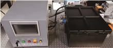
Through the research and design of the detection system, optical system and vacuum chamber of the vacuum ultraviolet spectral radiometer, a lightweight, miniaturized and highly sensitive vacuum ultraviolet spectral radiometer was developed. The spectral range, central wavelength and spectral radiance of the vacuum ultraviolet radiometer were tested. The test results showed that the spectral range of the radiometer covered the vacuum ultraviolet band of 115 nm~200 nm, and the maximum responsivity was around five working wavelengths of 121.2 nm, 135.6 nm, 160 nm, 180 nm and 200 nm, respectively. The vacuum ultraviolet spectral radiance of the radiometer in the full band was measured by using a calibrated deuterium lamp at 0.006 4~3.923 9 μW/cm2·nm·sr, and the measurement accuracy could reach 0.01 μW / cm2·nm·Sr.
Sep. 28, 2023Vol. 43 Issue 3 269 (2023)
Yan FENG, and Lei LU
A dual-camera monitor was proposed and a detection algorithm was designed for abnormal cheating behavior in exams, which detected four common exam abnormal behaviors of candidates, such as: carrying prohibited items, surrogate exam-taker, speaking during the exam, and drifting of candidates' attention. Firstly, the attention‑based YOLOv5s algorithm was used to detect prohibited items in exams. Then, Dlib‑based facial recognition was applied to confirm the candidates' identity information. Finally, lip movement detection and head pose estimation were utilized to detect abnormal behavior of candidates during the exam. The use of dual cameras could reduce blind spots in the field of view to prevent candidates from using cheating tools. The experiment results showed that the proposed algorithm had good detection accuracy and real-time performance.
Sep. 28, 2023Vol. 43 Issue 3 276 (2023)
Qing LI, Omolola E. Fayemi, Jun XU, Kun WU, Jianming ZHOU, and Wei LEI
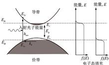
It was thoroughly investigated for the absorption of broadband incident light, photogenerated carrier generation, and the physical process of photogenerated carrier transport and compounding, and a number of semiconductor layers with different energy bandgaps were proposed to set up in the pin semiconductor junction in this paper. Through different energy bandgap semiconductor layers, the absorption region of incident light of different wavelengths could be adjusted, and the bias voltage could be used to control the transport and compounding of photogenerated carriers in different regions. Then the spectral response characteristics of the detector was improved. According to the results of the study, the Pearson correlation coefficient of the detector spectral response curve decreased from 0.99 to 0.68 at different bias voltages when four layers of intrinsic layers with bandgap gradient distributions were set up, providing effective broad-spectrum probing data for the subsequent spectral reconstruction of the detector.
Sep. 28, 2023Vol. 43 Issue 3 191 (2023)
Yifan DING, Yuning ZHANG, and Jin DING
LT7911D and LT9211 chips were selected as display bridge chips, which integrated power supply, data transmission, and audio-video signal transmission functions through Type-C interface. The debugging was easy,the process was mature, and it did not require a large area, which facilitated the miniaturization of the entire system. A micro image source driver system based on the STC MCU was implemented and the localization of display driver chips was achieved. At the same time, a fast adaptive Gamma correction algorithm was used to improve the display effect of micro image source and could make it better applied to the field of head mounted display.
Sep. 28, 2023Vol. 43 Issue 3 201 (2023)
Mengran FAN, Haixiang MA, and Xinzhong LI
The generation of a microscale chiral array light field based on Richards‑Wolf vector diffraction theory was realized by introducing a translational phase factor into the incident light. Through simulation research, the flexible regulation of array size and chirality of array subunits was further realized. In addition, the propagation characteristics of the array were explored, and the light field pattern distribution of the chiral array light field was maintained within the ±λ propagation distance. This study greatly enriches the mode of chiral intensity light field, and has good application prospects in the preparation of chiral micro‑nano materials.
Sep. 28, 2023Vol. 43 Issue 3 207 (2023)
Yifeng LIU, Junyang NIE, Kaixin ZHANG, Chang LIN, Min LI, Qun YAN, and Jie SUN
HfO2 films were successfully prepared by low-cost and easy-to-operate liquid deposition method, and the surface appearance, composition, optical characteristics, and electrical properties of HfO2 thin films generated by liquid deposition method were studied, as well as the reaction mechanism. The results revealed that the chemical composition of HfO2 thin films generated by liquid deposition method was pure and the structure was dense and continuous. The transmittance of HfO2 films after annealing at 500 ℃was greater than 92%; after making a plate capacitor with 40 nm hafnium oxide as the dielectric, the leakage current density at the voltage of 1 V was 3.56×10⁻⁷ A/cm2; the capacitance value at the 1 MHz frequency was 1.05 nF, yielding a calculated permittivity of 18.9.The successful preparation of hafnium oxide thin film by liquid deposition could provide a low-cost and simple method for using hafnium oxide thin film as the passivation layer of Micro LED devices.
Sep. 28, 2023Vol. 43 Issue 3 212 (2023)
Dalei WU, Tianwen XIA, Shaohang CHEN, Jiayi DU, Yongai ZHANG, Xiongtu ZHOU, Tailiang GUO, Qun YAN, and Jie SUN
The overall structure of the pixel points based on the quantum-dot color conversion film (QDCCF) was analyzed and designed using the simulation method. Firstly, the structure model of blue light micro light-emitting diode (Micro LED) was constructed. Besides, the surface microstructures, which included surface roughening and 2-D grating, were studied to enhance the light extraction efficiency (LEE) of the Micro LED. Moreover, the LEE and light intensity distribution of blue sub-pixels of the blue Micro LED with or without surface microstructure and the side-wall light-blocking medium under different side-wall angles were analyzed separately. Then, the parameters of the QDCCF were optimized, and the LEE and light intensity distribution of the red and green sub-pixels were analyzed in the Micro LED with different structures. Finally, the color shift of full-color pixels with different structures were compared and analyzed. The simulation results showed that the pixels with surface-roughening blue Micro LED and side-wall reflective light-blocking media could obtain a larger frontal LEE and a color shift of less than 0.02 at the angle of 0°~50°, which was more suitable for the QDCCF scheme compared with other structures.
Sep. 28, 2023Vol. 43 Issue 3 218 (2023)
Yibin LIN, Wandi CHEN, Jinjie XU, Shanshan JIANG, Yongai ZHANG, Chaoxin WU, Tailiang GUO, and Xiongtu ZHOU
The flexible ACEL device was fabricated on ITO/PET electrode using copper-doped zinc sulfide (ZnS: Cu) phosphor as luminescent molecule, polydimethylsiloxane (PDMS) and barium titanate (BaTiO3) as insulating material by scraping technology. The effects of different material mixing ratio, driving voltage and frequency of composite luminescent layer on the photoelectric properties of the device were studied. The results showed that the luminance of flexible ACEL devices increased with the increase of phosphor and barium titanate content. When ZnS: Cu/BaTiO3/PDMS=2∶ 2∶ 1, the device performance was the best, and the lower opening voltage could be achieved. The luminance could reach 1.16 cd/m2 at 40 V and 2 kHz. Finally, the flexible ACEL device was integrated with the vertical contact separation friction nanogenerator. The maximum output voltage and current of the TENG could reach 360 V and 46 µA, which could light up the flexible ACEL devices. The self-powered flexible ACEL devices could provide a new method for wearable display and interaction.
Sep. 28, 2023Vol. 43 Issue 3 226 (2023)
Wenbo LI, Wentao LI, Leming TANG, Yong YANG, Qiming XU, and Yanwei SHEN
The 230 nm far-UVC LED packaging device was fabricated, and the influence of the photoelectric performance and reliability by using fluorine resin for packaging were studied. The results showed that the optical power of 230 nm far-UVC LED packaging device with fluorine resin had a increase of 13%, which could reach 1 mW, and no influence was found in aging performance, while the photoelectric conversion efficiency was still less than 0.1%. After 216 h normal temperature aging, the light maintenance rate decreased to 45%. The application of 230 nm far-UVC device for detection of nitrate concentration was also evaluated. The results showed that when the concentration was lower than 15 mg/L, the absorbance in cm-1 showed a linear relationship with the concentration of the nitrate solution, which indicated that the 230 nm far-UVC device could be used in nitrate determination.
Sep. 28, 2023Vol. 43 Issue 3 233 (2023)
Zihong SHEN, Zunxian YANG, and Tailiang GUO
The photonic synaptic transistor of organic small molecule semiconductor TIPS-pentacene, polystyrene and perovskite quantum dots was prepared by the solution method using the domain limited induced crystallization method. The film structure and photoelectric properties of the film were researched, and the synaptic properties and behavior of the synaptic transistor were investigated under different light stimulation conditions. The polystyrene played a dual role in improving the crystallinity of organic small molecule semiconductor films and maintaining long-term photocurrent of synapse devices. At the same time, organic composite thin film devices have achieved graphic perception and memory functions, which could be of great significance for the development of artificial vision systems.
Sep. 28, 2023Vol. 43 Issue 3 238 (2023)
Jide ZHOU, Yimeng DOU, Liangwei SUN, Fan YANG, Chaojie LYU, and Kangkai XU
A folding optical system which was aimed to shorten the axial length of the low‑light‑level night vision goggles was designed to improve the wearing comfort. Firstly, the overall design was given, which included the design of a foldable objective lens, a long working range, and dual channel eyepiece system. Next, the parameters of the objective lens and eyepieces were obtained through the theoretical calculation. Finally, an initial structure that met the requirements was selected, and the folding optical system was optimized by using the software. Compared to the traditional direct‑view night vision goggles, the axial length of the night vision goggles was reduced from 110 mm to 70 mm by using folding optical system, which was closer to wearer’s head and could effectively improve wearing comfort.
Sep. 28, 2023Vol. 43 Issue 3 243 (2023)
Ting YE, Haoxiang LUO, Kefei ZHANG, and Weiguang LIU
A D-type photonic crystal fiber magnetic fluid double core filled magnetic field and temperature dual parameter measurement sensor structure was proposed. The resonance effect was enhanced and sensitivity was improved by narrowing the two holes in the center of the air hole in the first layer, the magnetic fluid-filled dual-core magnetic sensing channel and the ethanol-filled temperature-sensitive channel, which were introduced to achieve high-sensitivity sensing and dual-parameter sensing. The results showed that the sensor temperature was -30 ℃~50 ℃, the transmission peak temperature sensitivity was 1.239 nm/℃, and the linearity reached 0.995 7, while the loss peak temperature spectral sensitivity was 2.514 nm/℃, and the linearity reached 0.997 17. The external magnetic field was 10 mT~30 mT, the transmission peak magnetic field sensitivity was -3.799 nm/mT, the linearity was up to 0.997 27, and the temperature measurement error was 1.135%, the magnetic field measurement deviation was 6.67%, with high sensitivity, accurate measurement, compact structure and other features. This study could further optimize the design of D-type PCF-SPR dual-parameter demodulation sensor.
Sep. 28, 2023Vol. 43 Issue 3 248 (2023)
Hanqin YUAN, Qingmu TIE, Weixian ZHAO, Xumeng QIU, Sai ZHENG, Tiande WU, Chen WANG, and Bin YANG
Multi-layered conductive rubber was designed, aiming at the complicated process design of the filling material at the gap opening of the front shell of TFT-LCD. The metal particle filling layer with high conductivity was selected as the conductive surface layer, meanwhile the carbon cloth layer was used to realize the electromagnetic shielding function. Whereas, the flexible silicone rubber was used as the intermediate matrix layer. The synergy of low hardness and high conductivity of conductive rubber was achieved through multi-layered structure. Results showed that when the shore A hardness of silicone rubber was 30, the volume resistivity was 0.01 Ω·cm, which could meet the application requirements of sealing, waterproof and EMI shielding of TFT-LCD.
Sep. 28, 2023Vol. 43 Issue 3 255 (2023)
© Copyright 2018-2021 | Chinese Laser Press.
All Rights Reserved 沪ICP备15018463号-20