


After interaction with ultrafast laser pulses, the dielectric and metal materials will be modified due to the ultra-intense energy of ultrafast laser pulses, such as femtosecond (fs) laser, picosecond laser, and nanosecond (ns) laser[
Acta Photonica Sinica, Volume. 49, Issue 10, 1014002(2020)
Research on Fabrication and Optoelectronic Properties of Surface Modified Silicon by Ultrafast Laser Pulse
In order to extend the absorption edge of crystalline silicon to the near infrared band to meet the requirement of optical communication,the textured silicon was obtained by irradiation of nanosecond laser pulses. The surface morphology of modified silicon under irradiation with different laser fluence from 0.39 J/cm2 to 24 J/cm2 was investigated. Then, the optical properties including reflectance, transmittance, and absorptance of silicon samples by nanosecond laser irradiation with different laser fluence were measured. The results show that the absorptance below the bandgap of silicon enhances for all the textured silicon samples and it is up to 55% for near infrared light of 1 500 nm. Next, the thermal stability of infrared absorption for the textured silicon samples was investigated. The thermal annealing process at temperatures of 473~1 073 K can slightly reduce the absorptance below the bandgap of silicon and the magnitude of reduction only varied within 10%. Moreover, the dependence of reflectance, transmittance, and absorptance of modified silicon on the annealing temperature was studied on. Lastly, the crystal structures of modified silicon were determined by Raman spectroscope. After irradiation of nanosecond laser pulses, the crystalline silicon surface is disordered and amorphous or polycrystalline phases are formed. However, the crystal quality of textured silicon can be improved by post-thermal annealing process.
Keywords
0 Introduction
Silicon (Si), as one of the most important semiconductor materials, has been widely applied in the field of microelectronics[
1 Experimental details
N-Si (111) substrates with 250 μm thick and 3 000 Ω·cm resistivity were cleaned using a standard cleaning solution [
2 Results and discussion
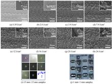
After irradiation of ns laser pulses with certain laser fluence, the Si surface is ablated and textured. Fig.1(a)~(h) show the surface morphologies of modified Si samples fabricated at different laser fluences of 0.39 J/cm2, 2.0 J/cm2, 3.9 J/cm2, 7.9 J/cm2, 12 J/cm2, 16 J/cm2, 20 J/cm2, and 24 J/cm2. For the laser fluence larger than melting threshold, Si substrate will absorb laser energy. After the lattice reaches temperatures exceeding the melting point of crystalline Si, a molten Si layer will develop. Melting followed by resolidification will change the atomic structure of Si materials [
After irradiation of higher laser fluences (>3.9 J/cm2) more substantial material will be removed from the Si surface and ablation damage becomes more observable. With increase of the laser fluence, the size of ablation zone increases. As a result, the adjacent scanning line overlaps each other. At the same time, the borderline is vague between the two adjacent lines, as a result the ablation zone corresponding to the shape of laser spot can not be observed clearly. The magnified details of the surface microstructures show as insets in Fig.1(a)~(h). Further increase the laser fluence can result in larger structures that go deeper into the material and many micro-spheres particles splashed from the adjacent lines in the Si surface. Furthermore, an increase of the laser fluence can also enlarge the diameters of the sputtered micro-spheres particles and surface roughness of textured Si. In addition, some secondary nanostructures are observed on the micro-spheres surface with the increase of the laser fluence. Fig.1(i) shows the pictures (15 mm ×15 mm) of real Si samples irradiated by ns laser pulses at different laser fluences. The used laser fluence of pictures A~H in Fig.1(i) correspond to that of Fig.1 (a)~(h), respectively. It can be found that the modified Si samples show different surface colours for the different laser fluence. Fig. 1 (j) shows pictures (1 mm×1 mm) of the real Si samples and the adopted laser fluence of pictures A~H in Fig.1(j) correspond to that of Fig.1(a)~(h), respectively. From these pictures, dimension of the whole melting zone increases with increase of laser fluence due to the heating effect of ns laser. A linear absorption process of ns laser pulse will lead deeper melt depths and slower resolidification-front speed, as a result the thermal ablation process of ns laser pulse will cause to the large heat-affected zone in Fig.1(j) [
The optical properties of Si samples are modified after the ablation of ns laser pulses. The reflectance (250~2 500 nm) of parts of Si samples is shown in Fig.2(a). From Fig.2(a), for all the modified samples, the reflectance above the bandgap of Si decreases (λ=250∼1 100 nm) when compared to the reflectance of crystalline Si substrate. The reduction of reflectance in this region can be attributed to scattering of incident light on the rough Si surface [
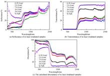
Similarly, the transmittance of Si samples in the range of 250~2 500 nm is shown in Fig.2(b). From Fig.2(b) it can be found that the irradiation of ns laser pulses don’t change the transmittance above the bandgap of Si (λ=250∼1 100 nm). In other words, the light in this region of wavelengths can not pass through the modified Si samples. However, after laser irradiation the transmittance below the bandgap of Si (λ=1 100∼2 500 nm) remarkable decreases. In addition, the transmittance of fabricated Si samples decreases firstly (<7.9 J/cm2) and then increases (>7.9 J/cm2) with the increase of laser fluence.
Then the absorptance of modified Si samples can be calculated according to energy conservation of light. The absorptance of modified Si samples and Si substrate is shown in Fig.2(c). In comparison with the absorptance of crystal Si substrate, the absorptance of modified Si samples obviously enhances in whole wavebands. For majority of modified samples the absorptance above the bandgap of Si is higher than 90%. Moreover, the absorptance in the range of 1 100~2 500 nm basically increases with increase of the laser fluence. For all the modified Si samples, the absorptance gradually decreases with increase of the wavelength in the range of 1 100~1 800 nm. The decrease of the absorptance is related to the structural defects induced by ns laser ablation [
In sum, for the modified Si samples, the reduction of reflectance and transmittance below the bandgap of Si can be attributed to the increase of light absorption. In addition, the absorption below the bandgap of Si are mainly induced by two mechanisms: Urbach states from α-Si in the re-solidified surface layer [
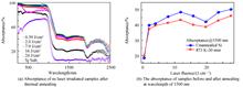
To investigate the thermal stability of NIR absorption of ablated Si by ns laser pulses, the modified Si samples have been thermally annealed at temperature of 873 K for 30 min. The absorptance of modified Si samples is shown in Fig.3(a). The absorptance below the bandgap of Si is slightly reduced by the annealing process (magnitude of reduction is lower than 10%) while the absorptance above the bandgap of Si nearly doesn't change after the thermal annealing. In comparison with the absorptance of unannealed Si samples, the absorptance of the annealed samples do not gradually decrease with increase of the wavelength (1 100~1 800 nm), which is related to reduced density of defect states in modified Si layer by the annealing process. However, the dependence of absorptance on laser fluence is nearly the same as the one before annealing. In order to clearly observe the variation tendency of absorptance of modified Si samples vs laser fluence, the dependence of sample's absorptance at 1 500 nm on the laser fluence (0.39~28 J/cm2) is described in Fig.3(b). The absorptance (18.3%) is low for the Si sample ablated by laser fluence of 0.39 J/cm2 while the absorptance (39.9%) rapidly rises for the sample irradiated under laser fluence of 2.0 J/cm2. Then, the absorptance of samples basically increases with increase of the laser fluence. After annealing, the variation of absorptance vs laser fluence shows similar tendency to that before annealing. But the annealing process reduces the absorptance of all the modified Si samples. For example, the absorptance decreases from 48.6% to 43.5% for the sample irradiated under laser fluence of 12 J/cm2.
To determine the dependence of optical properties on annealing temperature, the modified Si samples have been thermally annealed at different temperatures (473~1 073 K) for the same duration time (30 min). Using a high-temperature tubular furnace, the samples were annealed at a flowing Ar atmosphere (99.999%) with pressure of 1 atm. The reflectance and transmittance of annealed Si sample (irradiated by ns laser pulses at fluence of 12 J/cm2) show as Fig.4(a) and (b), respectively. Annealing at 473 K nearly does not affect optical properties of the samples, thus the optical properties of 473 K are not provided in the Fig.4. After annealing at the temperature of 473~873 K, the reflectance above the bandgap of Si is almost unaltered. As a contrast, the reflectance below the bandgap of Si increases with increase of the annealing temperature. However, after annealing at the temperature of 1 073 K the reflectance of modified Si sample has little variation in the whole measured range. Next, from Fig.4(b), the transmittance above the bandgap of Si does not change after annealing at all the temperatures, whereas the transmittance below the bandgap of Si increases with increase of the annealing temperature (473~873 K). It is interesting that further increasing temperature (1 073 K) will oppositely reduce the transmittance of modified Si samples.
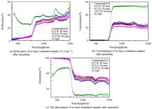
The absorptance of annealed samples is calculated in Fig.4(c). Similarly, thermal annealing process nearly doesn't impact the absorptance above the bandgap of Si. But the annealing process can reduce the absorptance below the bandgap of Si for the annealing temperature of 473~873 K. In addition, the NIR absorptance of modified Si sample decreases with increase of the annealing temperature. In contrary, the absorptance of annealed Si samples at the temperature of 1 073 K increases compared to one of unannealed Si sample. After thermal annealing at temperature of 473~873 K, the reduction of absorptance below the bandgap of Si can be attributed to the weakly thermal stability of defect states contributing to the NIR absorption. However, after annealing at higher temperature of 1 073 K, the enhanced absorptance maybe come from the point defects stabilized at high temperature and this phenomenon is called absorption reactivation [
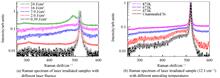
To clarify the structures of modified Si by ns laser pulses, the Raman spectroscopy of ablated Si samples is measured. Fig.5(a) is the Raman spectrum of Si surface layer irradiated by ns laser pulses at different fluences. From the Raman spectrum in Fig.5(a), all samples include a Raman vibration peak centred at 520 cm-1 corresponding to vibration of Si-Si atoms of the crystalline Si (Si-I) [
3 Conclusion
In this paper, nanosecond laser pulses have been used to modify the crystalline Si surface. From the SEM images, it can be found that the larger laser fluence will induce the larger surface roughness and larger-scale ablation, which is related to heating effect of nanosecond laser pulses. In addition, different surface colours have been observed for the real pictures of textured Si samples fabricated at different laser fluences. The study on optical properties indicates that the infrared absorptance of crystalline Si can be enhanced by nanosecond laser irradiation and the infrared absorptance increases with increase of the laser fluence within the specific limits. Although the thermal annealing process can slightly reduce the infrared absorptance of textured Si, the magnitude of reduction in the absorptance is unobvious. Furthermore, the infrared absorptance decreases with increase of the annealing temperatures until 873 K. Finally, from the measurement for Raman spectroscopy, the crystal structures of modified Si by nanosecond laser pulses have been changed. The Si surface has been disordered by the melting and resolidification process. Next, the amorphous or polycrystalline phases have been formed in the disordered Si surface layer. Consequently, the infrared absorption of samples may be related to these new phases formed in the modified Si layer. Further thermal annealing will improve the crystal quality of modified Si with the reduction of density of defect states in Si surface layer.
[1] C HNATOVSKY, R S TAYLOR, P P RAJEEV. Pulse duration dependence of femtosecond-laser-fabricated nanogratings in fused silica. Applied Physics Letters, 87, 14104(2005).
[2] Ji-hong ZHAO, Chun-hao LI, Jun-jie XU. Surface modification of nanostructured ZnS by femtosecond laser pulsing. Applied Surface Science, 293, 332-335(2014).
[3] A Y VOROBYEV, C GUO. Enhanced absorptance of gold following multipulse femtosecond laser ablation. Physical Review B, 72, 195422(2005).
[4] A WECK, T H R CRAWFORD, D S WILKINSON. Laser drilling of high aspect ratio holes in copper with femtosecond, picosecond and nanosecond pulses. Applied Physics A, 90, 537-543(2008).
[5] Yong-guang HUANG, Shi-bing LIU, Wei LI. Two-dimensional periodic structure induced by single-beam femtosecond laser pulses irradiating titanium. Optics Express, 17, 20756-20761(2009).
[6] A BOROWIEC, H K HAUGEN. Subwavelength ripple formation on the surfaces of compound semiconductors irradiated with femtosecond laser pulses. Applied Physics Letters, 82, 4462-4464(2003).
[7] F COSTACHE, S KOUTEVA-ARGUIROVA, J REIF. Sub-damage-threshold femtosecond laser ablation from crystalline Si: surface nanostructures and phase transformation. Applied Physics A, 79, 1429-1432(2004).
[8] R LE HARZIC, H SCHUCK, D SAUER. Sub-100 nm nanostructuring of silicon by ultrashort laser pulses. Optics Express, 13, 6651-6656(2005).
[9] J BONSE, M MUNZ, H STURM. Structure formation on the surface of indium phosphide irradiated by femtosecond laser pulses. Journal of Applied Physics, 97, 13538(2005).
[10] T G KIM, J M WARRENDER, M J AZIZ. Strong sub-band-gap infrared absorption in silicon supersaturated with sulfur. Applied Physics Letters, 88, 241902(2006).
[11] A KOHNO, S CHARNVANICHBORIKARN. Fabrication and subband gap optical properties of silicon supersaturated with chalcogens by ion implantation and pulsed laser melting. Journal of Applied Physics, 107, 123506(2010).
[12] I UMEZU, J M WARRENDER, S CHARNVANICHBORIKARN. Emergence of very broad infrared absorption band by hyperdoping of silicon with chalcogens. Journal of Applied Physics, 113, 213501(2013).
[13] S H PAN, D RECHT, S CHARNVANICHBORIKARN. Enhanced visible and near-infrared optical absorption in silicon supersaturated with chalcogens. Applied Physics Letters, 98, 121913(2011).
[14] W T HSIAO, S F TSENG, K C HUANG. Pulsed Nd:YAG laser treatment of monocrystalline silicon substrate, 56, 223-231(2011).
[15] S BINETTI, A LE DONNE, A ROLFI. Picosecond laser texturization of mc-silicon for photovoltaics: A comparison between 1064 nm, 532 nm and 355 nm radiation wavelengths. Applied Surface Science, 371, 196-202(2016).
[16] S SARBADA, Zhi-feng HUANG, Y C SHIN. Low-reflectance laser-induced surface nanostructures created with a picosecond laser. Applied Physics A, 122, 1-10(2016).
[17] A J PEDRAZA, J D FOWLKES, D H LOWNDES. Silicon microcolumn arrays grown by nanosecond pulsed-excimer laser irradiation. Applied Physics Letters, 74, 2322-2324(1999).
[18] G MASINI, L COLACE, G ASSANTO. 55 μm. Applied Physics Letters,, 82, 2524-2526(2003).
[19] P R CHIDAMBARAM, C BOWEN, S CHAKRAVARTHI. Fundamentals of silicon material properties for successful exploitation of strain engineering in modern CMOS manufacturing. IEEE Transactions on Electron Devices, 53, 944-964(2006).
[20] S REGGIANI, E GNANI, A GNUD. Low-field electron mobility model for ultrathin-body SOI and double-gate MOSFETs with extremely small silicon thicknesses. IEEE Transactions on Electron Devices, 54, 2204-2212(2007).
[21] R J FINLAY, C WU. Microstructuring of silicon with femtosecond laser pulses. Applied Physics Letters, 73, 1673-1675(1998).
[22] C WU, C H CROUCH, L ZHAO. Near-unity below-band-gap absorption by microstructured silicon. Applied Physics Letters, 78, 1850-1852(2001).
[23] B R TULL, M T WINKLER, E MAZUR. The role of diffusion in broadband infrared absorption in chalcogen-doped silicon. Applied Physics A, 96, 327-334(2009).
[24] Ji-hong ZHAO, Chun-hao LI, Qi-dai CHEN. Femtosecond laser direct writing assisted nonequilibriumly doped silicon n+-p photodiodes for light sensing. IEEE Sensors Journal, 15, 4259-4263(2015).
[25] Ji-hong ZHAO, Chun-hao LI, Xian-bin LI. NIR photodetector based on nanosecond laser-modified silicon. IEEE Transactions on Electron Devices, 65, 4905-4909(2018).
[26] C H CROUCH, J E CAREY, J M WARRENDER. Comparison of structure and properties of femtosecond and nanosecond laser-structured silicon. Applied Physics Letters, 84, 1850-1852(2004).
[27] R J YOUNKIN. Surface studies and microstructure fabrication using femtosecond laser pulses(2001).
[28] M J SHER, M T WINKLER, E MAZUR. Pulsed-laser hyperdoping and surface texturing for photovoltaics. MRS Bulletin, 36, 439-455(2011).
[29] K C PHILLIPS, H H GANDHI, E MAZUR. Ultrafast laser processing of materials: A review. Advances in Optics and Photonics, 7, 684-712(2015).
[31] Jing YANG, Fang-fang LUO. Design and fabrication of broadband ultralow reflectivity black Si surfaces by laser micro/nanoprocessing. Light: Science & Applications, 3, e185(2014).
[32] Chun-hao LI, Ji-hong ZHAO, Xin-yue YU. Fabrication of black silicon with thermostable infrared absorption by femtosecond laser. IEEE Photonics Journal, 8, 1-9(2016).
[33] B R TULL, M T WINKLER, E MAZUR. The role of diffusion in broadband infrared absorption in chalcogen-doped silicon. Applied Physics A, 96, 327-334(2016).
[34] W B JACKSON, N M AMER. Direct measurement of gap-state absorption in hydrogenated amorphous silicon by photothermal deflection spectroscopy. Physical Review B, 25, 5559-5562(1982).
[35] Chun-hao LI, Ji-hong ZHAO, Qi-dai CHEN. Infrared absorption of femtosecond laser textured silicon under vacuum. IEEE Photonics Technology Letters, 27, 1481-1484(2015).
[36] A BARHDADI, B HARTIT, J C MULLER. Active defects generated in silicon by laser doping process. African Review Physics, 6, 229-238(2011).
[37] B K NEWMAN, M J SHER, E MAZUR. Reactivation of sub-bandgap absorption in chalcogen-hyperdoped silicon. Applied Physics Letters, 98, 251905(2011).
[38] Ji-hong ZHAO, Xian-bin LI, Qi-dai CHEN. Ultrafast laser induced black silicon, from micro-nanostructuring, infrared absorption mechanism, to high performance detecting devices. Materials Today Nano, 11, 100078(2020).
[39] Chao LI, Ji-hong ZHAO, Xi CHEN. Investigation of the structure and optical absorption of silicon coated with a chromium film after femtosecond laser irradiation, 35, 015019(2020).
Tools
Get Citation
Copy Citation Text
Yang YANG, Chao LI, Ji-hong ZHAO. Research on Fabrication and Optoelectronic Properties of Surface Modified Silicon by Ultrafast Laser Pulse[J]. Acta Photonica Sinica, 2020, 49(10): 1014002

Paper Information
Category: Lasers and Laser Optics
Received: Apr. 28, 2020
Accepted: Jun. 30, 2020
Published Online: Mar. 10, 2021
The Author Email:

© Copyright 2018-2021 | Chinese Laser Press.
All Rights Reserved 沪ICP备15018463号-20