


 View fulltext

2025
Volume: 8 Issue 1
5 Article(s)
Zhi Jiang, Cizhe Fang, Xu Ran, Yu Gao, Ruiqing Wang, Jianguo Wang, Danyang Yao, Xuetao Gan, Yan Liu, Yue Hao, and Genquan Han
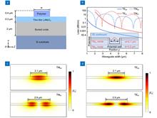
The expansive spectral coverage and superior optical properties of lithium niobate (LN) offer a comprehensive suite of tools for exploring novel functionalities. Achieving high-quality (Q) photonic resonator cavities is crucial for enhancing light-matter interactions. However, this task is challenging as the device performance is heavily dependent on the fabrication quality of the LN. In this paper, we present experimental validation of an etchless approach to fabricating high-Q photonic crystal nanobeam cavities (PCNBCs). We successfully fabricate PCNBCs with Q factors exceeding 105 while maintaining high transmittance by capitalizing on the low waveguide loss and high fabrication tolerance of TE-polarized mode. Remarkably, the Q factor achieved here exceeds previous reports on etchless LN PCNBCs by over an order of magnitude. Benefiting from this advancement, we further explore a variety of optical functions, including thermo-optic tuning, optically induced bistability, and Fano line shapes generation. These findings present promising prospects for a versatile platform technique, facilitating the development of high-performance electro-optic or acousto-optic modulators, optical logic devices, and quantum photonics, highlighting its significant impact in the field of photonic integration.
Jan. 23, 2025Vol. 8 Issue 1 240114-1 (2025)
Changdi Zhou, Yu Huang, Yigong Yang, Deyu Cai, Pei Zhou, Kuenyao Lau, Nianqiang Li, and Xiaofeng Li
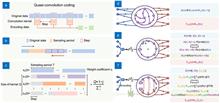
Photonic platforms are gradually emerging as a promising option to encounter the ever-growing demand for artificial intelligence, among which photonic time-delay reservoir computing (TDRC) is widely anticipated. While such a computing paradigm can only employ a single photonic device as the nonlinear node for data processing, the performance highly relies on the fading memory provided by the delay feedback loop (FL), which sets a restriction on the extensibility of physical implementation, especially for highly integrated chips. Here, we present a simplified photonic scheme for more flexible parameter configurations leveraging the designed quasi-convolution coding (QC), which completely gets rid of the dependence on FL. Unlike delay-based TDRC, encoded data in QC-based RC (QRC) enables temporal feature extraction, facilitating augmented memory capabilities. Thus, our proposed QRC is enabled to deal with time-related tasks or sequential data without the implementation of FL. Furthermore, we can implement this hardware with a low-power, easily integrable vertical-cavity surface-emitting laser for high-performance parallel processing. We illustrate the concept validation through simulation and experimental comparison of QRC and TDRC, wherein the simpler-structured QRC outperforms across various benchmark tasks. Our results may underscore an auspicious solution for the hardware implementation of deep neural networks.
Jan. 23, 2025Vol. 8 Issue 1 240135-1 (2025)
Cheng-Long Zheng, Pei-Nan Ni, Yi-Yang Xie, and Patrice Genevet
Semiconductor optoelectronics devices, capable of converting electrical power into light or conversely light into electrical power in a compact and highly efficient manner represent one of the most advanced technologies ever developed, which has profoundly reshaped the modern life with a wide range of applications. In recent decades, semiconductor technology has rapidly evolved from first-generation narrow bandgap materials (Si, Ge) to the latest fourth-generation ultra-wide bandgap semiconductor (GaO, diamond, AlN) with enhanced performance to meet growing demands. Additionally, merging semiconductor devices with other techniques, such as computer assisted design, state-of-the-art micro/nano fabrications, novel epitaxial growth, have significantly accelerated the development of semiconductor optoelectronics devices. Among them, integrating metasurfaces with semiconductor optoelectronic devices have opened new frontiers for on-chip control of their electromagnetic response, providing access to previously inaccessible degrees of freedom. We review the recent advances in on-chip control of a variety of semiconductor optoelectronic devices using integrated metasurfaces, including semiconductor lasers, semiconductor light emitting devices, semiconductor photodetectors, and low dimensional semiconductors. The integration of metasurfaces with semiconductors offers wafer-level ultracompact solutions for manipulating the functionalities of semiconductor devices, while also providing a practical platform for implementing cutting-edge metasurface technology in real-world applications.
Jan. 23, 2025Vol. 8 Issue 1 240159-1 (2025)
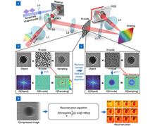
Yizhao Meng, Yu Lu, Pengfei Zhang, Yi Liu, Fei Yin, Lin Kai, Qing Yang, and Feng Chen
Single-shot ultrafast compressed imaging (UCI) is an effective tool for studying ultrafast dynamics in physics, chemistry, or material science because of its excellent high frame rate and large frame number. However, the random code (R-code) used in traditional UCI will lead to low-frequency noise covering high-frequency information due to its uneven sampling interval, which is a great challenge in the fidelity of large-frame reconstruction. Here, a high-frequency enhanced compressed active photography (H-CAP) is proposed. By uniformizing the sampling interval of R-code, H-CAP capture the ultrafast process with a random uniform sampling mode. This sampling mode makes the high-frequency sampling energy dominant, which greatly suppresses the low-frequency noise blurring caused by R-code and achieves high-frequency information of image enhanced. The superior dynamic performance and large-frame reconstruction ability of H-CAP are verified by imaging optical self-focusing effect and static object, respectively. We applied H-CAP to the spatial-temporal characterization of double-pulse induced silicon surface ablation dynamics, which is performed within 220 frames in a single-shot of 300 ps. H-CAP provides a high-fidelity imaging method for observing ultrafast unrepeatable dynamic processes with large frames.
Jan. 23, 2025Vol. 8 Issue 1 240180-1 (2025)
Junkyeong Park, Gyeongtae Kim, and Junsuk Rho
Spatial computing and augmented reality are advancing rapidly, with the goal of seamlessly blending virtual and physical worlds. However, traditional depth-sensing systems are bulky and energy-intensive, limiting their use in wearable devices. To overcome this, recent research by X. Liu et al. presents a compact binocular metalens-based depth perception system that integrates efficient edge detection through an advanced neural network. This system enables accurate, real-time depth mapping even in complex environments, enhancing potential applications in augmented reality, robotics, and autonomous systems.
Jan. 23, 2025Vol. 8 Issue 1 240267-1 (2025)
© Copyright 2018-2021 | Chinese Laser Press.
All Rights Reserved 沪ICP备15018463号-20