


 View fulltext

2024
Volume: 7 Issue 4
6 Article(s)

Dingyu Xu, Wenhao Xu, Qiang Yang, Wenshuai Zhang, Shuangchun Wen, and Hailu Luo
Apr. 25, 2024Vol. 7 Issue 4 230120C (2024)
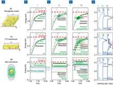
Mikhail A. Masharin, Daria Khmelevskaia, Valeriy I. Kondratiev, Daria I. Markina, Anton D. Utyushev, Dmitriy M. Dolgintsev, Alexey D. Dmitriev, Vanik A. Shahnazaryan, Anatoly P. Pushkarev, Furkan Isik, Ivan V. Iorsh, Ivan A. Shelykh, Hilmi V. Demir, Anton K. Samusev, and Sergey V. Makarov
Deeply subwavelength lasers (or nanolasers) are highly demanded for compact on-chip bioimaging and sensing at the nanoscale. One of the main obstacles for the development of single-particle nanolasers with all three dimensions shorter than the emitting wavelength in the visible range is the high lasing thresholds and the resulting overheating. Here we exploit exciton-polariton condensation and mirror-image Mie modes in a cuboid CsPbBr3 nanoparticle to achieve coherent emission at the visible wavelength of around 0.53 μm from its ultra-small (≈0.007 μm3 or ≈λ3/20) semiconductor nanocavity. The polaritonic nature of the emission from the nanocavity localized in all three dimensions is proven by direct comparison with corresponding one-dimensional and two-dimensional waveguiding systems with similar material parameters. Such a deeply subwavelength nanolaser is enabled not only by the high values for exciton binding energy (≈35 meV), refractive index (>2.5 at low temperature), and luminescence quantum yield of CsPbBr3, but also by the optimization of polaritons condensation on the Mie resonances with quality factors improved by the metallic substrate. Moreover, the key parameters for optimal lasing conditions are intermode free spectral range and phonons spectrum in CsPbBr3, which govern polaritons condensation path. Such chemically synthesized colloidal CsPbBr3 nanolasers can be potentially deposited on arbitrary surfaces, which makes them a versatile tool for integration with various on-chip systems.
Apr. 25, 2024Vol. 7 Issue 4 230148 (2024)
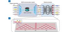
Yuanjian Wan, Xudong Liu, Guangze Wu, Min Yang, Guofeng Yan, Yu Zhang, and Jian Wang
In recent years, space-division multiplexing (SDM) technology, which involves transmitting data information on multiple parallel channels for efficient capacity scaling, has been widely used in fiber and free-space optical communication systems. To enable flexible data management and cope with the mixing between different channels, the integrated reconfigurable optical processor is used for optical switching and mitigating the channel crosstalk. However, efficient online training becomes intricate and challenging, particularly when dealing with a significant number of channels. Here we use the stochastic parallel gradient descent (SPGD) algorithm to configure the integrated optical processor, which has less computation than the traditional gradient descent (GD) algorithm. We design and fabricate a 6×6 on-chip optical processor on silicon platform to implement optical switching and descrambling assisted by the online training with the SPDG algorithm. Moreover, we apply the on-chip processor configured by the SPGD algorithm to optical communications for optical switching and efficiently mitigating the channel crosstalk in SDM systems. In comparison with the traditional GD algorithm, it is found that the SPGD algorithm features better performance especially when the scale of matrix is large, which means it has the potential to optimize large-scale optical matrix computation acceleration chips.
Apr. 25, 2024Vol. 7 Issue 4 230182 (2024)
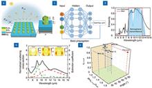
Yinan Zhang, Yinggang Chen, Tong Wang, Qian Zhu, and Min Gu
Real-world passive radiative cooling requires highly emissive, selective, and omnidirectional thermal emitters to maintain the radiative cooler at a certain temperature below the ambient temperature while maximizing the net cooling power. Despite various selective thermal emitters have been demonstrated, it is still challenging to achieve these conditions simultaneously because of the extreme difficulty in controlling thermal emission of photonic structures in multidimension. Here we demonstrated hybrid polar dielectric metasurface thermal emitters with machine learning inverse design, enabling a high emissivity of ~0.92 within the atmospheric transparency window 8–13 μm, a large spectral selectivity of ~1.8 and a wide emission angle up to 80 degrees, simultaneously. This selective and omnidirectional thermal emitter has led to a new record of temperature reduction as large as ~15.4 °C under strong solar irradiation of ~800 W/m2, significantly surpassing the state-of-the-art results. The designed structures also show great potential in tackling the urban heat island effect, with modelling results suggesting a large energy saving and deployment area reduction. This research will make significant impact on passive radiative cooling, thermal energy photonics and tackling global climate change.
Apr. 25, 2024Vol. 7 Issue 4 230194 (2024)
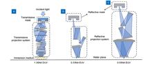
Ziqi Li, Lisong Dong, Xu Ma, and Yayi Wei
Extreme ultraviolet (EUV) lithography with high numerical aperture (NA) is a future technology to manufacture the integrated circuit in sub-nanometer dimension. Meanwhile, source mask co-optimization (SMO) is an extensively used approach for advanced lithography process beyond 28 nm technology node. This work proposes a novel SMO method to improve the image fidelity of high-NA EUV lithography system. A fast high-NA EUV lithography imaging model is established first, which includes the effects of mask three-dimensional structure and anamorphic magnification. Then, this paper develops an efficient SMO method that combines the gradient-based mask optimization algorithm and the compressive-sensing-based source optimization algorithm. A mask rule check (MRC) process is further proposed to simplify the optimized mask pattern. Results illustrate that the proposed SMO method can significantly reduce the lithography patterning error, and maintain high computational efficiency.
Apr. 25, 2024Vol. 7 Issue 4 230235 (2024)
Manukumara Manjappa, and Yuri Kivshar
Recent experiments suggest a novel approach for engineering robust and efficient high-Q resonances in THz metasurfaces opening new avenues for applications in hyperspectral sensing.
Apr. 25, 2024Vol. 7 Issue 4 240043 (2024)

© Copyright 2018-2021 | Chinese Laser Press.
All Rights Reserved 沪ICP备15018463号-20