


Please enter the answer below before you can view the full text.

Bowang Shu, Yuqiu Zhang, Hongxiang Chang, Qi Chang, Pengfei Ma, Jinyong Leng, and Pu Zhou
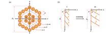
ObjectiveLaser scanning technologies are applied into numerous fields, such as free space optical communication, LIDAR, laser processing, and remote imaging. Therefore, it is important in military equipment and industrial manufacturing. Currently, most laser scanning technologies are realized by silicon-based photo-electronics, liquid crystal spatial light modulator, micro electro mechanical system (MEMS), and coherent laser arrays, etc. Among them, coherent laser arrays are proved to be an efficient method for generating laser with high power, brightness, and beam quality. Owing to designable coherent laser arrays and flexible phase controlling algorithm, remarkable progress in scanning technologies has been realized. In 2022, Zhou et al. utilized constant piston phase differences between -π and π to control the positions of far-field light spots, with limited maximum scanning angle and relatively low diffraction efficiency. In 2021, construction of quasi-continuous scanning system with the combination of micro-lens arrays and adaptive fiber optics collimators (AFOCs) was proposed. Such a system realizes controllable tilting-phase mainly by AFOCs. However, only experimental results of one-dimensional quasi-continuous scanning patterns are provided. Thus, it is urgent to study more possibilities in the customization of any light field patterns and determine the detailed scanning characteristics under the condition of huge coherent laser array to satisfy additional application requirements.MethodsThe method of two-dimensional continuous scanning is mainly based on the regular hexagonal arrangement of coherent laser arrays. Then, the phase modulation mode is set as the sawtooth titling phase corresponding to maximum optical path differences, which belongs to a type of blazed grating phase-controlling mode. When the maximum optical path differences of adjacent sub-apertures increase, their phase differences increase, i.e., the tilting phase in single sub-aperture can sustain periodic change compared to constant piston phase. Therefore, the beam will deflect an angle of θduring transmission as the wavefront iso-phase surface tilts at a certain angle of θ.Results and DiscussionsUsing typical coherent laser arrays with 19, 127, and 919 sub-apertures shown in Fig. 6, simulated results of single scanning point locating at γ=0, γ=π/2, γ=π/4, and γ=-π/4 are displayed in Figs. 7‒9, respectively. Utilizing these single scanning points, two-dimensional quasi-continuous scanning can be realized along x, y, y=x, and y=-x axes, as illustrated in Fig. 10. All patterns show clear outlines, evenly distributed energy, and a smooth curved effect. Owing to the advantages of this tilting phase-controlling model, specific scanning patterns (S, B, and W) are constructed by switching the distributed phase calculated in advance (Fig. 11). Barring the scanning patterns achieved by coherent laser arrays, spatial scanning characteristics are further studied. Owing to the linear relationships between the tilting phase and the scanning angles, the steering angles of far-field beams continuously increase as the tilting phase experiences more periods. Thus, the scanning angles have no limitations under ideal conditions. Moreover, the scanning straight lines with average distributed energy indicate that near-unity diffraction efficiency can be achieved by tilting phase-controlled coherent laser arrays. Most importantly, the number of sub-apertures shows no influence on the diffraction efficiency, energy distribution, and scanning scope. With increasing number of sub-apertures, the scanning precision is improved owing to the larger caliber of coherent laser arrays. Although the grating lobes exist near the central bright spots, the increased sub-apertures can avoid the interferences to some extent because of long distances among them. Notably, the focused energy of far-field spots is higher as the number of sub-apertures increases, which is beneficial in obtaining scanning pattens with better performance.ConclusionsWith the regulation of tilting wavefront, coherent laser arrays can realize periodical phase change within a single sub-aperture to achieve single scanning points at any position, quasi-continuous scanning, and customized specific optical field patterns in a two-dimensional plane. Compared to the piston phase-controlling model, the scanning characteristics of coherent laser array with the controlled tilting phase are optimized. First, the diffraction efficiency can reach one theoretically. Second, the scanning range is not limited under the ideal condition. Last, the far-field spot energy and scanning precision can be further improved by increasing the number of sub-apertures. This work can provide significant guidance in terms of fast optical field coverage and target tracking, and scanning technologies will develop towards direction of non-mechanical mode, large steering angle, high precision, and anti-interference. In future, more studies will be performed in this regard, including reducing the influence of gate lobe, realizing the customization of arbitrary optical field pattern, and expanding the function of coherent laser arrays.
Jan. 25, 2024Vol. 51 Issue 2 0205001 (2024)
Dimming Controllable Hybrid Multilayer OFDM Modulation Method for Indoor Visible Light Communication
Jiawei Ren, Tao Wang, Zhijian Xu, and Jing Qu
ObjectiveIndoor visible light communication systems generally need to provide both communication and lighting services, and in order to meet the standard requirements for indoor lighting, indoor visible light communication systems must have brightness control (also called dimming control). Therefore, it is imperative to design indoor visible light signal modulation methods that can perform dimming control. Indoor high-speed visible light communication often uses orthogonal frequency division multiplexing (OFDM) modulation to achieve high-speed transmission, and traditional optical OFDM research mainly focuses on improving data transmission rate, which cannot effectively support dimming control, resulting in poor user experience. Therefore, dimmable OFDM modulation schemes adapted to communication-lighting integrated applications need to be designed. In OFDM dimming design, a balance between transmission efficiency and dimming capability is required. Direct current biased optical OFDM (DCO-OFDM) controls the brightness level directly by controlling the DC bias level, but it may limit and thus corrupt the signal waveform. By superimposing layered asymmetrically clipped optical OFDM (LACO-OFDM) with multiple positives and negatives, it achieves both dimming and improved spectral efficiency by using the multi-layer transmission. However, the multi-layer superposition characteristic of LACO-OFDM leads to a relatively high peak-to-average-power ratio and deteriorating the bit error rate (BER) performance at specific dimming levels.MethodsFor the lighting demand and dimming requirement of visible light communication, this paper proposes a hybrid superimposed LACO-OFDM (HSLACO-OFDM) modulation method based on LACO-OFDM modulation. According to the principle of LACO-OFDM signal formation and subcarrier occupancy in each layer, it can be seen that after the superposition of signals in the Lth layer, there will still be some subcarriers that are not used. The superposition of the adjusted signals on these subcarriers does not interfere with the signals of the LACO-OFDM layers. Therefore, we can design a time domain amplitude adjustment of the LACO-OFDM signal after superimposing the signals using these subcarriers to generate the superimposed LACO-OFDM (SLACO-OFDM) signal. For SLACO-OFDM signals, the receiver can detect the signal layer by layer using the same method of successive interference cancellation as for LACO-OFDM signal detection. By combining SLACO-OFDM and its negative signal NSLACO-OFDM through time division multiplexing, the HSLACO-OFDM signal is formed. The proposed HSLACO-OFDM makes full use of the entire dynamic range of light emitting diodes (LEDs) with adjustable mixed signal ratios to achieve the desired brightness. We propose an optimal setting of the HSLACO-OFDM interlayer power scaling factor using a Lagrangian function under a certain constraint of electrical power. It is also proved that the optimal ratio should be the same in each layer because the parameters are the same in different layers, when the signal transmission rate reaches the maximum. We also investigate the HSLACO-OFDM hybrid scaling factor determination method under dimming constraints. The two degrees of freedom of the dimming factor are analyzed, and the method of taking values under different dimming levels is given.Results and DiscussionsSimulations are performed to evaluate the performance of the proposed HSLACO-OFDM. It is also compared with DCO-OFDM, reconstructed LACO-OFDM (RLACO-OFDM), and adaptively biased layered optical OFDM (ABLO-OFDM). The BER performances of 4-layer HSLACO-OFDM and LACO-OFDM with 16-ary quadrature amplitude modulation (QAM), 32-ary QAM (32QAM) and 64-ary QAM (64QAM) modulation are simulated (Fig.6). At the same QAM modulation order, the BER decreases and then increases as the dimming factor changes from 1 to 6.5. The main reason is that as the dimming factor increases, the limiting noise of the signal decreases and the BER improves. However, too large dimming factor can also lead to a smaller signal power, resulting in a deterioration of the BER performance. And the dimming factor can be taken as the value corresponding to the smallest BER. From the results, it can be seen that the proposed HSLACO-OFDM signal has better BER performance compared with LACO-OFDM under the same simulation parameters. The spectral efficiency of HSLACO-OFDM under the condition of dimming constraint is simulated (Figs.7 and 8). For the same number of layers, the proposed scheme can achieve higher spectral efficiency than the conventional RLACO-OFDM and ABLO-OFDM for intermediate dimming levels. From the simulation results, it can be summarized that for HSLACO-OFDM, the optimal number of stacked layers varies with the noise power and dimming level. In low brightness and high brightness or high noise environments, a lower number of stacked layers should be used. When working in medium dimming level and low noise environment, more stacked layers can be used.ConclusionsIn order to realize the dimming control of visible light communication, this paper designs the HSLACO-OFDM dimming modulation based on SLACO-OFDM low peak-to-average-power ratio multilayer superposition modulation by combining SLACO-OFDM and NSLACO-OFDM signals. The hybrid ratio calculation method under the minimum BER and dimming constraints is given. The proposed HSLACO-OFDM makes full use of the entire dynamic range of LEDs with adjustable mixing signal ratio to achieve the desired brightness. Since HSLACO-OFDM has a lower peak-to-average-power ratio, a relatively stable transmission efficiency can be obtained over a wide adjustable range of light brightness. Simulation results show that this scheme has advantages over other commonly used multilayer modulation and dimming OFDM schemes in terms of BER performance and spectrum utilization.
Feb. 25, 2024Vol. 51 Issue 2 0206001 (2024)
Xiaoke Yin, Le He, Shaokun Liu, Yingbo Chu, Nengli Dai, and Jinyan Li
ObjectiveWith the rapid application of 5G, big data, cloud computing, internet of things (IoT), and other technologies, the demand for data traffic has greatly increased in recent decades. Current optical fiber amplifiers are no longer able to cope with the capacity crunch in communication systems, and extending the gain bandwidth of the amplifier is considered an economical and feasible solution. However, commercially available erbium-doped fiber amplifiers (EDFA) can only achieve optical amplification in the C-band and the L-band, and 1260‒1500 nm band is under-exploited. Recently, bismuth-co-doped glasses and fibers have attracted attention because of their various luminescence characteristics based on different host materials, which cover the wavelength range of most communication transmission windows. Currently, bismuth co-doped phosphosilicate fibers have great potential in the second transmission window (1260‒1360 nm) owing to their excellent compatibility with silica communication fibers. Therefore, bandwidth extension using Bi-doped phosphosilicate fibers is an effective solution for increasing transmission capacity.MethodsBecause of the characteristics of bismuth ions, such as unstable chemical valence and sensitivity to the glass matrix, it is difficult to prepare Bi-doped silica-based fibers. In this study, we demonstrate a Bi-doped phosphosilicate fiber fabricated using modified chemical vapor deposition (MCVD) technology. The refractive index profile of the preform is measured. The preform is then drawn to a fiber with core diameter/cladding diameter of 9 μm/120 μm. Optical parameters, such as background loss and absorption spectra, are recorded. Moreover, the ratio of the unsaturated loss to small-signal absorption indicates the extrinsic loss level of the Bi-doped fibers, which is measured by testing the output power variation with increasing pump power. Finally, an all-fiber experimental configuration of a Bi-doped fiber amplifier is constructed to evaluate the amplification properties of the fiber based on the single stage with forward-pumping scheme.Results and DiscussionsTo ensure adequate optical properties, the refractive index profile of the fiber is measured, and a cutoff wavelength of 1000 nm is calculated with a refractive index difference between the core layer and cladding layer of 0.0045. The absorption coefficient of 0.55 dB/m at 1240 nm and the background loss of 21 dB/km at 1500 nm are measured using the standard cutback method, and no significant water peak is observed. In addition, the variation in loss with increasing pump power is measured to estimate the unsaturated loss and the ratio of the unsaturated loss to small-signal absorption, which are 0.079 dB/m and 13.6%, respectively. The results indicate that only a small fraction of bismuth ions form inactive centers to induce loss, whereas most of them form bismuth active centers associated with phosphorus(BACs-P). Finally, the amplification characteristics of the Bi-doped fibers are measured using a single-stage amplifier configuration with a forward-pumping scheme. With the signal power of -15 dBm and the pump power of 460 mW at 1240 nm, the maximum gain of 21.2 dB is achieved using a fiber length of 140 m. A net gain with a bandwidth (1270‒1480 nm) covering the O-band and E-band is obtained, and the 3 dB bandwidth from 1310 nm to 1365 nm is also achieved. It can be observed that the gain in the O-band is significantly greater than that in the E-band; thus, we believe the difference is attributable to the higher concentration of BACs-P than that of bismuth active centers associated with silicon (BACs-Si).ConclusionsWe report a bismuth co-doped phosphosilicate fiber fabricated using MCVD technology. The maximum gain of 21.2 dB is achieved at 1340 nm for the 460 mW pump power of a 1240 nm laser diode and the signal power of -15 dBm in the single-stage and forward-pumping amplifier configuration. Meanwhile, a net gain bandwidth from 1270 nm to 1480 nm covering the O+E band is achieved, and the 3 dB bandwidth is approximately 55 nm.
Jan. 25, 2024Vol. 51 Issue 2 0206002 (2024)
Penghao Zhang, Hongbo Wu, Shuang Chen, Wensong Jiang, and Li Zhang
ObjectiveFiber Bragg gratings (FBGs) fabricated by femtosecond laser have the advantages of light weight, high capacity wavelength division multiplexing, high mechanical strength, and excellent thermal stability. As a significant sensitive component of sensors, FBGs have been deployed widely in aerospace, nuclear power, metallurgy, bridges, and tunnels. One common method of their construction is directly writing FBGs point by point; however, this suffers from high loss. Various techniques have been proposed to reduce this loss, such as improving the writing path to line by line, shaping femtosecond laser beams, and selecting optical fibers with smaller core diameters. Despite reductions in loss, there remain deficiencies in their production, such as low fabrication efficiency and generality. In this study, an inscription method of FBG based on a small-aperture beam shaping technique has been proposed, which can be helpful for the efficient fabrication of low-loss FBGs.MethodsFirst, the energy distribution of a focused Gaussian beam limited by aperture is analyzed, and the aperture condition of the filamentary focal field is obtained. A femtosecond laser writing device based on small aperture shaping is then built. When the aperture is gradually reduced from 10.0 mm to 0.5 mm, a series of second-order FBGs are written on standard quartz single-mode fibers with the coating removed. The lengths of the FBGs are 3 mm, the reflectivities are approximately 90%, and the center wavelengths are near 1550 nm. The microscopic images of the FBG are obtained via a charge coupled device (CCD) camera along and perpendicular to the laser incidence direction. The corresponding transmission spectra are obtained by an FBG interrogator.Results and DiscussionsAs the aperture decreases, the length of the grating fringes perpendicular to the laser incidence direction increases significantly faster than along the incidence direction; the shapes of the grating fringes thus gradually change from elliptical to filamentous. When the aperture is 10.0 mm, the insertion loss and short-wavelength loss (at 1510 nm) are 0.9 dB and 4.01 dB, respectively; when the aperture is reduced to 1.0 mm, these two types of losses decrease to 0.11 dB and 0.35 dB, respectively (Fig. 5). This is because the filamentous grating fringe reduces the curvature of the typical circular fringe, leading to less Mie scattering of incident light. At the same time, because the area of the coupling between the filamentous grating fringes and the fundamental mode of the fiber is greater, the same coupling amplitude requires smaller refractive index modulation. Therefore, the small aperture has a significant suppression effect on losses. The short-wavelength loss of FBG manifests in the form of oscillation over a wide spectral range, mainly due to the excitation of cladding modes by refractive index perturbations in the grating region, which are coupled with the fundamental mode of the fiber core. The oscillation amplitude mainly depends on the energy of the low azimuth cladding mode. When the aperture is reduced to 1.0 mm, the filamentous fringes have a smooth refractive index modulation, resulting in the lower excitation of high-azimuth cladding modes but the higher excitation of some low-azimuth cladding modes (Fig. 7). The low-azimuth cladding modes carry more energy, resulting in higher coupling efficiency with the fundamental mode of the core. The oscillation is reduced by writing an FBG on a coated fiber or an FBG with a relatively low reflectivity (such as 40%; Fig. 9).ConclusionsIn this study, a low-loss femtosecond fiber grating fabrication technology based on small aperture shaping is proposed. The filamentous shaping effect of the small aperture on the grating fringe is theoretically analyzed and experimentally demonstrated. A series of FBGs with a central wavelength of 1550 nm and a reflectivity of 90% are fabricated by using different apertures. As the aperture is reduced from 10.0 mm to 1.0 mm, the grating fringe shape gradually transitions from circular to filamentous, while the insertion loss is reduced from 0.90 dB to 0.11 dB and the short-wavelength loss is reduced from 4.01 dB to 0.35 dB. Compared to circular grating fringes, the filamentous grating fringes reduce the Mie scattering of incident light and enhance the coupling of fundamental modes of the core, effectively reducing loss. The filamentous fringes also enhance the excitation of low-azimuth cladding modes, leading to greater oscillations at the short-wavelength side. These oscillations can be effectively suppressed by writing an FBG on a coated fiber or an FBG with a relatively low reflection.
Jan. 25, 2024Vol. 51 Issue 2 0206003 (2024)
Tao Yang, Xue Wang, Kaixuan Li, Bingjie Zhang, Yu Shi, Shuyang Chen, and Xinpei Chen
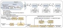
ObjectiveWavelength division multiplexing (WDM) optical networks include numerous wavelengths and nodes, dynamic reconfiguration of transmission paths, and dynamic scheduling of services/resources. Thus, a low-cost and highly reliable online monitoring technology is urgently required to ensure the safe and stable operation of WDM networks. It is the cornerstone technology to ensure the safe and efficient operation of the optical network and effectively reduce operation and maintenance costs. Currently, optical network monitoring obtains the spectral information of each channel using devices such as tunable optical filters. From this information, the channel performance such as the optical modulation format and optical signal-to-noise ratio (OSNR) can be obtained. Another scheme uses a high-speed service signal coherence receiver with complex digital signal processing (DSP) to monitor the channel performance; however, this method can only realize the end-to-end optical performance parameter monitoring of a single wavelength channel. The timeliness of monitoring cannot be guaranteed. Exciting schemes generally have problems such as high cost, poor monitoring reliability, inability to monitor the wavelength channel status at intermediate nodes in real time, and complex system structures. They cannot meet the requirements of low-cost and high-reliability optical performance monitoring for the new generation of large-scale complex optical networks. To address these problems, a low-cost and high-efficiency optical performance monitoring scheme based on a quadratic pulse amplitude modulation (PAM4) optical label is proposed for WDM optical networks.MethodsThis paper proposed an optical performance monitoring scheme based on the PAM4 optical label that uses a PAM4 modulation format digital label to carry more monitoring information and improve the timeliness of optical network monitoring. Using the DSP unit at the service transmitter, time-domain digital labels with specific frequency pilot tones were loaded flexibly into the corresponding wavelength channels without the need for additional digital-to-analog converters (DACs) or custom optical modulators. Approximately 1% optical power was separated using an optical coupler at the monitoring node. Subsequently, a low-bandwidth photodetector (PD) and a low-speed analog-to-digital converter (ADC) were used to receive optical labels from all channels. Using a specially designed optical label demodulation and processing algorithm, the optical power and OSNR of all the wavelength channels could be obtained accurately. Simultaneously, the digital label monitoring information loaded onto the corresponding wavelength channel could be recovered. Thus, the low-cost and highly reliable monitoring of the wavelength channel performance was achieved.Results and DiscussionsA simulation platform of a 16 GBaud polarization multiplexing (PM) QPSK/16QAM WDM optical transmission system for a C-band eight-channel 25-span transmission was built to verify the feasibility and accuracy of the proposed WDM optical network monitoring scheme based on the PAM4 optical label. The simulation results show that the method of calculating the channel optical power [Fig. 5(b)] using the peak of the spectrum at the pilot tone significantly reduces the power monitoring error caused by the complex high-order harmonics in the PAM4 digital label compared with the method of spectral integral using the OOK/DPSK label. Moreover, the correction of the label mean value significantly reduces the monitoring error caused by the uneven label distribution [Fig. 5(c)]. After the 25-span long-distance transmission, the channel optical power monitoring error does not exceed 0.65 dB [Fig. 5(d)], the OSNR estimation error does not exceed 0.6 dB (Fig. 6), and the performance is slightly better than that based on low-order modulation format optical label such as DPSK (Fig. 7). The experimental results show that the power monitoring errors of the QPSK and 16QAM systems are less than 0.3 dB when different label modulation depths and different mean values of digital label signals are used in a 80 km optical transmission.ConclusionsTo meet the requirements of multi-channel, multi-parameter, low-cost, and highly reliable online monitoring for WDM optical networks, a new monitoring scheme based on the PAM4 digital optical label is proposed. We innovatively proposes a complete set of mechanisms for loading, detecting, and processing the PAM4 optical label, as well as an error correction method for optical power monitoring based on the PAM4 optical label sequence characteristics. It can accurately and efficiently monitor the optical power and OSNR of all wavelength channels in real time. Based on the established WDM multi-channel and multi-span transmission simulation platform, the monitoring performance after a 25-span WDM optical transmission was simulated and analyzed. The results show that the performance of the proposed PAM4 label-based optical power monitoring is significantly improved using the designed power monitoring error correction method. The maximum optical power error does not exceed 0.65 dB, and the OSNR estimation error does not exceed 0.6 dB. The performance of the proposed PAM4 label-based monitoring scheme is slightly better than those of the DPSK and OOK low-order optical label-based monitoring schemes. In addition, an offline experimental platform was constructed using a PD with a bandwidth of 200 MHz and an ADC with a sampling rate of 400 MSa/s. The experimental results show that the PAM4 label can be accurately recovered using the proposed scheme, and the optical power monitoring error is less than 0.3 dB. These results demonstrate that the proposed scheme is cost-effective, easy to deploy on a large scale, reliable, and efficient for WDM optical network monitoring.
Jan. 25, 2024Vol. 51 Issue 2 0206004 (2024)
Shaokun Liu, Le He, Xiaoke Yin, Yingbo Chu, Nengli Dai, and Jinyan Li
ObjectiveThe advent of optical communication technology in the information age has significantly increased data traffic demand. However, the current fiber communication backbone, which employs wavelength-division multiplexing (WDM) and erbium-doped fiber amplifiers (EDFAs), utilizes only the C+L bands (1520‒1620 nm) with a bandwidth of approximately 100 nm, resulting in a low efficiency of 20% in spectrum bandwidth resource utilization. To effectively use the O, E, S, and U bands other than C+L bands, communication networks must be equipped with optical fiber amplifiers to amplify the signals in the corresponding bands to compensate for transmission loss. However, to date, no fiber amplifier exists that can effectively satisfy the commercial requirements of these frequency bands. To further expand fiber amplifier gain bandwidth, germanosilicate bismuth-doped fibers have attracted attention owing to their unique luminescence characteristics, which are expected to address the commercial requirements of communication in E+S bands. However, because of the unknown formation mechanism and source of luminescent active centers (i.e., active bismuth ions) in germanosilicate bismuth-doped fibers, the mass fraction of effective active bismuth ions in the fibers is low (<10-4). As a result, the lengths of fibers used in the E- and S-bands range from 150 m to 320 m, compared to the 5‒10 m length of commercial EDFA fibers, making the application cost of germanosilicate bismuth-doped fibers and the miniaturization difficulty of manufacturing devices significantly higher. Therefore, it is necessary to study high-absorption germanosilicate bismuth-doped fibers to expand their transmission bandwidths and shorten their lengths.MethodsIn this study, the modified chemical vapor deposition (MCVD) method combined with liquid-phase doping is used to fabricate germanosilicate bismuth-doped fibers. The small-signal absorption spectra of the germanosilicate bismuth-doped fibers are measured through the standard truncation method. The Bi and Ge doping concentrations are measured using an electron probe microanalyzer (EPMA). The unsaturated fiber loss is characterized using an unsaturable loss (UL) test system (Fig. 2). In addition, a multi-wavelength division multiplexing light source (1330‒1510 nm, interval of 20 nm) is used as the signal, and a single-stage forward pump structure (Fig. 4) is constructed to test the bismuth-doped fiber gain performance (Fig. 5) and efficiency (Fig. 6). The input pump power (wavelength of 1310 nm) and total input signal power are 367 mW and -20 dBm, respectively.Results and DiscussionsAs shown in Fig. 2, the absorption peak height of the bismuth-doped fiber is higher than that of the optical fiber sold in Russia (OFSR). At a wavelength of 1310 nm, it is 1.16 dB/m, which is 3.87 times higher than that (0.3 dB/m) of the OFSR for small signals. The effective absorption of BACs-Si in small signal absorption is further determined by measuring the unsaturated absorption coefficient at 1310 nm, which is only 0.19 dB/m, accounting for 16.4% of small signal absorption (Fig. 3). The absorption attributed to the bismuth active centers (BACs-Si) is subsequently calculated by subtracting UL (0.19 dB/m) from the small signal absorption (1.16 dB/m) at 1310 nm, yielding a value of 0.97 dB/m. Figure 5 shows that the peak gain of the bismuth-doped fiber is 33 dB at a wavelength of 1450 nm when the fiber length is 65 m. As the fiber length decreases, the gain peak gradually increases at 1450 nm and subsequently slowly decreases. This is because in long fibers, amplified shortwave signals are reabsorbed, producing long-wave signals. However, as the fiber length decreases, the reabsorption of the shortwave signal weakens, resulting in a strengthened shortwave and slightly decreased long-wave signal. Consequently, the 20 dB gain bandwidth widens slightly as the fiber length decreases. The specific 20 dB gain range for fiber lengths of 70, 65, 60, 55, and 50 m are 60, 63, 63, 63, and 65 nm, respectively, as shown in Table 2. Figure 6 shows the gain and gain efficiency of the bismuth-doped fibers at a wavelength of 1450 nm for different pumping powers when the fiber length is 65 m. The gain efficiency ranges from 0.09 dB/mW to 0.23 dB/mW, and the gain coefficient per unit length reaches 0.51 dB/m.ConclusionsIn this study, the preparation and characteristics of a high-absorption germanosilicate bismuth-doped fiber are described. The fiber has a high concentration of BACs-Si and low UL, with small signal absorption at 1310 nm of 1.16 dB/m and UL at 1310 nm of only 0.19 dB/m, accounting for 16.4% of small signal absorption. A high-absorption germanosilicate bismuth-doped fiber is prepared based on the MCVD method and solution doping technology. When the total input power is -20 dBm and the forward input pump power is 367 mW at 1310 nm, the 50 m long optical fiber achieves a gain of over 20 dB at 1414‒1479 nm. The maximum gain of 33 dB is achieved at 1450 nm when the fiber length is 65 m, and the gain efficiency ranges from 0.09 dB/mW to 0.23 dB/mW at different pumping powers. At 65 m length, the gain reaches its maximum (33 dB) at 1450 nm, and the gain coefficient per unit length reaches 0.51 dB/m. Compared to existing reports, the fiber usage length is significantly reduced, and the gain level is further improved.
Jan. 25, 2024Vol. 51 Issue 2 0206005 (2024)
Keyu Yang, Weilu Sun, Junkai Sheng, Qianqian Peng, Shengchuang Bai, Shixun Dai, and Xunsi Wang
ObjectiveBragg fibers have multiple unique optical properties such as photonic bandgap light guides, single-mode transmission over a wide frequency range, dispersion management, and low transmission loss, which make them attractive for broad applications. The transmission ability of a traditional hollow Bragg fiber is restricted by air-core collapse and structured-cladding deformation during optical fiber preparation. Even under tiny fiber cladding deformations, the bandgap can be violently degraded. All solid-state structures have been proven to solve the core collapse and cladding deformation problems of hollow Bragg fibers. Therefore, an urgent requirement exists to develop novel fiber structures and effective fiber fabrication methods to improve fiber transmission capability. In this study, an all-solid Bragg fiber with a chalcogenide glass core is fabricated via a compensated-stacking extrusion technique to address the challenge of hollow-core deformation in traditional Bragg fibers. The fiber consists of three pairs of uniform periodic cladding and low-loss windows in the range of 4‒10 μm. This experimental data can assist further study regarding mid-infrared bandgap-controlled fibers and unlock new directions for the development of high-quality laser transmissions or optical sensors in the mid-infrared region.MethodsIn this study, we first establish a theoretical model for all-solid-state Bragg fibers. Mid-infrared chalcogenide glasses Ge20As20Se15Te45 and As2S3 are chosenas high- and low-refractive-index cladding materials. The large difference in the refractive index between the alternating-layer materials helps to form the widest photonic bandgap. Two groups of fibers based on equal- or compensated-thickness glass are prepared for comparison. The cross sections, transmission loss values, and near-field energy distributions of these optical fiber types are calculated and analyzed.Results and DiscussionsAccording to the simulation results, the optimal structural parameters of all solid-state chalcogenide Bragg fibers are obtained. The experimental results show that optimized stacking extrusion based on compensated-thickness glass is the simplest and most effective method for improving fiber structural uniformity. The cross-sections of the all-solid Bragg fiber based on equal-thickness glass [Figs. 7(a)‒(c)] show that the core and innermost cladding are irregularly elliptical, with a large difference in the thickness of the three pairs of periodic claddings. The thickness of the layers ranges from 10 μm to 600 μm, which significantly differs the simulation results [Fig. 8(a)]. The fiber cross-sections based on thickness-compensated glass [Figs. 7(d)‒(f)] show that the fiber structure is highly circular, without deformation, and no obvious defects such as bubbles or holes are observed at the interfaces of adjacent layers. Three pairs of periodic claddings have similar thicknesses in a 6-meter-long fiber, and the average ratio of each layer thickness to the fiber diameter is approximately 3∶100 for an entire fiber length with 6 m length [Fig. 8(b)]. It is proven experimentally that it is feasible to solve the problem of uneven claddings and deformational cores using thickness-compensated glass. The average loss of fibers based on equal-thickness glass is 4 dB/m‒6 dB/m, however, the uneven fiber structure results in light propagation in the cladding [Fig. 9(a)]. The fiber based on thickness compensated glass has four low loss windows [Fig. 9(b)]. For good light transmission effect, the light is confined in the core and almost no energy leaks into the cladding.ConclusionsBragg fibers based on the principle of effective omnidirectional reflection achieve high-power transmission at specific wavelengths by tuning the structural parameters of the claddings; however, some problems remain. In this study, an all-solid-state Bragg fiber with a chalcogenide glass core is fabricated using a compensated stacking extrusion technique to solve the problem of hollow core deformation in traditional Bragg fibers. Ge20As20Se15Te45 and As2S3 glasses are doped as high- and low-refractive-index cladding materials, respectively, and an all-solid-state chalcogenide glass Bragg fiber with three pairs of periodic cladding layers is successfully fabricated via compensated stacking extrusion. The superior structural uniformity of the prepared chalcogenide Bragg fibers is verified by comparing the cross-sections of the front, middle, and end of the Bragg fibers. Three pairs of periodic claddings have similar thicknesses in a 6-meter-long fiber, and the average ratio of each layer thickness to the fiber diameter is approximately 3∶100 for an entire fiber with length of 6 m. The light spot pattern proves that the optical fiber has good light transmission ability.It is proven experimentally that it is feasible to prepare chalcogenide Bragg fibers using the extrusion method. In future, our research will further improve the extrusion mold and conditions aiming to develop higher performance photonic crystal fibers based on chalcogenide glass.
Jan. 25, 2024Vol. 51 Issue 2 0206006 (2024)
Xu Liu, Fangru Zhong, Xinning Ma, and Peng Zhang
ObjectiveLaser acquisition, pointing, and tracking (APT) technology is prevalent in the realm of space optical communication, servicing platforms such as inter-satellites, satellite-ground, airborne, and ship-borne. By fusing coarse and fine tracking, it is possible to achieve picometer-scale, high-probability, swift, and accurate dynamic space-optical communications. However, the application of APT in underwater wireless optical communication remains underreported. This limited application stems from the APT system’s intricate, precise, sizable, and costly nature, which challenges the minimalist design needs of underwater wireless optical communication systems. Additionally, the underwater channel’s resistance, pressure, and environmental adaptability factors compromise the servo control system’s precision and pose engineering challenges. These challenges curtail the expansion and application of APT technology in underwater wireless optical communication. Thus, harnessing APT technology to enhance the stability and reliability of communication links by capturing and tracking the optical axis emerges as a promising avenue in underwater wireless optical communication’s future. Consequently, there’s a pressing need to devise a servo control system that’s both cost-effective and straightforward, catering specifically to the dynamic underwater wireless optical communication’s acquisition and tracking demands.MethodsIn this study, we first considered the basic concept of space optical communication acquisition, pointing, and tracking technology. Based on this, we proposed a set of acquisition and tracking systems grounded in servo control for underwater wireless optical dynamic communication. Subsequently, we studied key technologies, including the servo control system architecture, composition model, and motor control algorithm. For the servo control system we proposed, a tracking differentiator was introduced within the active disturbance rejection control algorithm to manage the motor’s acceleration and deceleration. Furthermore, we proposed a coarse and precise tracking strategy that utilized motor acceleration and deceleration control technology. Ultimately, we discussed the acquisition time, tracking accuracy, and acquisition probability of the servo control system we proposed, drawing insights from both simulations and actual indoor and underwater experiments.Results and DiscussionsIn the simulation experiment, the upper computer receives miss distance information and transmits it to the lower computer via the virtual serial port, controlling the motor. The upper computer displays the motor’s working state in real-time on the upper computer (Fig.5) and simulates the spot capture and tracking of underwater wireless optical dynamic communication. When the simulated spot occupies a different position, the motor adaptively accelerates and decelerates, achieving both coarse and precision tracking. The motor operates stably before and after acceleration and deceleration, without missteps (Table 2, Fig. 7). The feasibility of the servo control system and tracking differentiator in executing motor acceleration and deceleration algorithm strategies is confirmed. In the indoor experiment, results indicate that the system captures and tracks the target spot within 4 s at its fastest rate. The azimuth motor’s tracking accuracy is 0.08 mrad (Fig.10) and that of the pitch motor’s is 0.27 mrad (Fig.11), aligning with tracking index requirements. The speed mutation curve for the azimuth and pitch motors during the experiment (Fig.12) reveals that the motor navigates via high-speed coarse tracking, variable-speed, and then low-speed precision tracking phases. The consistent operation surrounding the variable speed affirms the algorithm’s feasibility, suggesting this system’s potential for underwater wireless optical dynamic communications. The underwater experiment reveals that the system captures the target spot in 8 s before disturbance, which is more than the acquisition time of the indoor system. Post-disturbance, the spot experiences interference from water body scattering and refraction, showing a dynamic state. The system completes target spot capture and tracking within 10 s, a duration extended from its pre-disturbance counterpart. Data analysis highlights a 0.6 mrad tracking accuracy for the servo control system before introducing disturbance to the water tank and a 2 mrad accuracy post-disturbance (Fig.14). Additionally, experiments demonstrate a capture probability surpassing 99% for the system. If the spot’s moving speed falls below the specified range in both horizontal and vertical directions, then the servo control stabilizes tracking; otherwise, the tracking fails.ConclusionsIn this study, we examine an acquisition and tracking servo control system for an underwater wireless optical dynamic communication system. We design a servo control system architecture and explore its constitute and control algorithm. We propose a control algorithm based on a tracking differentiator to achieve motor acceleration and deceleration. Concurrently, we employ motor acceleration and deceleration technology to implement a coarse and precise tracking strategy for the underwater wireless optical dynamic communication optical axis. We conduct simulation verifications, indoor tests, and underwater laser spot acquisition and tracking experiments. The underwater laser spot acquisition and tracking experiment reveals that the system’s acquisition probability exceeds 99%, with an acquisition time of less than 10 s. The tracking accuracy, both before and after the water tank disturbance, registers at 0.6 mrad and 2 mrad, respectively. This experiment demonstrates that the designed servo control system aligns with the performance index requirements, setting the stage for further research into underwater wireless optical dynamic communication technology.
Jan. 25, 2024Vol. 51 Issue 2 0206007 (2024)
Yi Huang, Yue You, Haosen Zhang, Chuanlu Deng, Chengyong Hu, Lisen Wang, Xiaobei Zhang, and Tingyun Wang
ObjectiveBecause of their advantages of small size, light weight, and long lifespan, tunable semiconductor lasers have broad application prospects in the fields of coherent optical communication, fiber optical sensing, and gas sensing. In recent years, extensive research on laser-tuning methods has been conducted for various application scenarios. Modulated grating Y-branch (MG-Y) lasers have been widely studied owing to their wide tuning range, fast tuning speed, and high flexibility. To achieve the wavelength-tuning function of the MG-Y laser in practical applications, a wavelength-current look-up table (LUT) must be developed. A common method of constructing an LUT is to scan the reflector currents, which is inefficient. In this method, the LUT contains a large number of invalid wavelength data points. This is not conducive to regular calibration and makes it difficult to ensure wavelength accuracy. The wavelength-tuning characteristics of the MG-Y laser were investigated, and the tuning method was optimized to address the issues of low efficiency in constructing the wavelength-current LUT, the complexity of wavelength-tuning methods, and the large power drift during the wavelength tuning of the MG-Y laser.MethodsFirst, the current characteristics of an MG-Y laser are analyzed. According to the principle of the additive Vernier effect of the MG-Y laser, adjusting the reflector currents can control the position of the comb reflection spectrum and realize a wavelength-coarse tuning function. Second, a universal wavelength testing framework is designed by utilizing the tuning characteristics of the left and right reflector currents and the principle of the orthogonal experiment. Third, a wavelength-tuning method based on a wavelength test framework is developed. All smooth wavelength-tuning paths can be obtained by scanning the reflector currents along the grid lines of the test framework. A wavelength-tuning range of 40 nm can be obtained by scanning the reflector currents along all smooth paths. A fine wavelength-tuning function is realized using the phase current of the MG-Y laser. Finally, a self-adaptive power calibration algorithm for wavelength tuning is developed. Using the principle of internal current loop feedback and based on the difference between the laser power feedback voltage and the threshold voltage, the laser output power calibration function is realized by self-adaptive adjustment of the current of the semiconductor optical amplifier.Results and DiscussionsOnly 3147 reflector wavelength combinations are included in the LUT built on the wavelength test framework, which greatly improves the efficiency of the LUT construction and reduces the number of invalid data points. A tuning performance test system and an optical fiber extrinsic Fabry-Perot interferometric (EFPI) cavity length demodulation system are used to evaluate the wavelength-tuning performance of the MG-Y laser. To verify the accuracy and effectiveness of the optimized wavelength-tuning method, the wavelength accuracy is tested first. The laser is tuned from 1528 nm to 1568 nm in step of 5 pm at room temperature for 8001 wavelength points. Good spectral quality is observed using the spectrometer, with no side-mode suppression ratio (SMSR) of less than 40 dB or wavelength jumps. The wavelength accuracy is better than ±2.9 pm with a standard deviation of 0.726 pm, and the laser also exhibits good linearity in output wavelength when tuned to 5 pm. In addition, the repeatability of the wavelength is tested. To improve the testing efficiency, the tuning step of the laser is set to 5 nm, and the laser is continuously tuned 30 times from 1530 nm to 1565 nm. The results show that the maximum drift at the same wavelength is only 1.9 pm, while the minimum drift is 0.4 pm. The output power of the laser is measured using an optical power meter, and the laser power is set to approximately 11.46 mW. Before calibration, the power drift can reach as high as 2.382 mW in one C-band scan, with a stability of 20.69%; after calibration, the maximum power drift is only 0.408 mW, with a stability of 3.57%. Finally, the accuracy and effectiveness of the optimized wavelength-tuning method and the superiority of the MG-Y laser-tuning performance are verified through an optical fiber EFPI cavity length demodulation experiment. The maximum fluctuation of the EFPI cavity length error is 7.58 nm, with a standard deviation of 1.60 nm after scanning the C-band 30 times continuously. The results verify the accuracy and effectiveness of the optimized wavelength-tuning method and the excellent tuning performance of the MG-Y laser in practical applications.ConclusionsThe wavelength-tuning characteristics of the MG-Y laser are investigated. Based on the tuning characteristics of the left and right reflector currents of the laser, a universal wavelength test framework is designed to locate all smooth tuning paths of the laser quickly and realize the fine-tuning function of the wavelength using the phase area currents. An adaptive power calibration algorithm is proposed to reduce the power drift of the laser during wavelength tuning. The results show that the LUT constructed based on the wavelength test framework contains only 3147 reflector current-wavelength combinations, the LUT construction method is simplified, and the number of invalid data in the table is considerably reduced. The wavelength-tuning range of the laser is 1528?1568 nm, the SMSR is greater than 40 dB, the offset between the actual wavelength and the set wavelength is less than ±2.9 pm, and the standard deviation is 0.726 pm. The wavelength repeatability is better than 1.9 pm after continuous wavelength tuning is performed 30 times. The maximum power drift during wavelength tuning is only 0.408 mW after power calibration, and the stability is 3.57%. The maximum fluctuation of the EFPI cavity length error is 7.58 nm, which can be applied to optical fiber EFPI spectral acquisition and cavity length demodulation experiments. The results show that the optimized wavelength-tuning method significantly improves the construction efficiency of the LUT of the MG-Y laser while simultaneously improving the power stability of the laser during wavelength tuning, which has good practical application value.
Jan. 25, 2024Vol. 51 Issue 2 0201001 (2024)
Bo Yao, Dian Duan, Xian’an Dou, Yujun Chen, Xiaobing Liu, and Qinghe Mao
ObjectivePicosecond laser pulses, characterized by their high peak power and spectral purity, hold significant importance in numerous applications across various fields. Mode-locked fiber lasers, with their compact structure, maintenance-free operation, and superior anti-interference ability, have emerged as one of the most vital sources of picosecond pulse lasers. Among these, SESAM and Figure-9 mode-locked fiber lasers have attracted significant attention owing to their exceptional self-start performance. Furthermore, in precision measurement applications, such as lidar and precision distance measurement, it is imperative to maintain a locked repetition rate of the laser pulse. However, practical engineering applications present novel challenges due to their complex environments, which include temperature changes ranging from -40 ℃ to 50 ℃ across different seasons, violent vibrations during transportation and usage, and stringent requirements concerning volume, weight, and power consumption. These conditions pose challenges to maintaining a locked repetition rate of the picosecond mode-locked fiber laser while ensuring the self-start function. Consequently, the design and development of a picosecond fiber laser with rapid self-start and repetition-rate-locking capabilities becomes a significant issue that warrants further exploration and research.MethodsThe configuration of the Figure-9 fiber laser was chosen, and the intracavity nonlinearity was optimized to realize the fast self-start mode-locking function for the laser. A "constant temperature" local-environment for the optical module was established by adiabatically packaging with low-thermal-conductivity materials. This approach significantly relaxed the requirement of the tuning range for the piezoelectric transducer (PZT) frequency tuning mechanism to lock the repetition rate of the fiber laser operating in the outdoor environment. Based on these advancements, a prototype mode-locked fiber laser weighing only 3 kg was designed and developed. This prototype showcased a typical repetition rate and pulse width of 10 MHz and 20 ps, respectively.ResultsAt room temperature, the measured pulse train, which displays a repetition rate of 10 MHz, is illustrated in Fig. 4(a). The intensity autocorrelation trace indicates the pulse width to be 20 ps [see Fig. 4(b)]. The pulse's center wavelength is 1064 nm with a 3 dB bandwidth of 0.2 nm (Fig. 4c). The repetition rate's fluctuation is less than 7.5 mHz over a 10 h test period [see Fig.5(a)]. The corresponding Allan variance of repetition-rate instability corresponds to 2.1×10⁻¹¹@1 s, 8.5×10⁻¹²@10 s, and 3.6×10⁻¹¹@1000 s [see Fig. 5(b)]. Repetition rates as a function of time are depicted in Fig.6(a) when the repetition rates are locked at -40 ℃, 0 ℃, and 50 ℃, respectively. The fluctuations of the repetition rates remain less than 15 mHz over a 30 min test period. Correspondingly, the Allan variance of repetition-rate instability is 4.3×10⁻¹¹, 5×10-11, and 2.8×10⁻¹¹ for 1 s at -40 ℃, 0 ℃, and 50 ℃, respectively [see Fig. 6(b)]. Fluctuations of repetition rates as functions of time are illustrated in Fig. 7(b) when the vibration is superimposed on each of the three coordinate axes, and the Allan variance for 1 s across these axes remains better than 2.5×10⁻¹⁰ [see Fig. 7(b)]. In an outdoor environment, the prototype's repetition rate can be locked for more than 3 h [see Fig. 8(c) and Fig. 8(d)], suggesting that the prototype can withstand temperature fluctuations of approximately 10 ℃ in an outdoor setting.ConclusionsA repetition-rate-locked picosecond pulsed fiber laser, designed for operation in outdoor environments, has been reported. The configuration of the Figure-9 fiber laser was chosen, and the intracavity nonlinearity was optimized to realize a fast self-start mode-locking function for the laser. A prototype of the mode-locked fiber laser, weighing only 3 kg and typically exhibiting a repetition rate and pulse width of 10 MHz and 20 ps respectively, was developed. Under varying conditions, such as room temperature, extreme ambient temperatures (-40 ℃ or 50 ℃), and environments experiencing vibrations of 1.5g, the prototype still managed to maintain self-start mode-locking and repetition-rate-locking. Furthermore, the prototype's repetition-rate-locking function demonstrated resistance to a 10 ℃ ambient temperature fluctuation when operating in high-temperature outdoor environments during summer.
Jan. 25, 2024Vol. 51 Issue 2 0201002 (2024)
Yuehao Han, Ruyi Feng, Youming Liu, Jinyang Zou, Bowen Liu, and Minglie Hu
ObjectiveIn recent years, with significant development in ultrashort pulse laser technology, femtosecond pulse lasers occupy an increasingly critical role in scientific research and industry. The overall tendency of femtosecond lasers is the higher peak power density, which is manifested by increasing pulse energy and reducing pulse duration. Multiple methods have been proposed to obtain femtosecond lasers with a pulse duration of <100 fs and a pulse energy of >10 μJ. In addition to Ti∶sapphire femtosecond lasers, which directly output femtosecond laser pulses with a high energy and short pulse duration, the compression of high-energy laser pulse output from Yb3+-doped femtosecond lasers is another pertinent method. Yb3+-doped fiber and solid-state femtosecond lasers output femtosecond laser pulses with higher average power, and therefore, show further application potential. However, owing to the gain bandwidth limitation, it is difficult to obtain laser pulses shorter than 300 fs. However, it is important to obtain femtosecond laser pulses with >100 μJ pulse energy and <100 fs pulse duration for many applications. To address this challenge, the nonlinear compression of femtosecond laser pulses is proposed, which improves the peak power density of laser pulses from Yb3+-doped femtosecond lasers. Thus, the proposed method enables further applications in industrial processing among other fields. However, some harmful effects exist which reduce nonlinear compression efficiency, such as conical emission. On the contrary, to increase nonlinear compression efficiency, it is important to suppress the conical emission and avoid nonlinear medium damage.MethodsIn this study, periodic layered Kerr media (PLKM) nonlinear compression principles are analyzed and experiments are conducted. For the conical emission effect in the nonlinear compression experiments, the harmful effect cause and its influence on nonlinear compression are experimentally studied. The spectrum broadening of pulse output from the Yb3+-doped femtosecond fiber laser is measured and analyzed. To weaken its influence on spectral broadening and nonlinear compression efficiency, phase shift distribution optimization during spectral broadening is proposed to suppress the obvious conical emission. The proposed method avoids the conical emission caused by the spectral broadening process in nonlinear compression. Subsequently, a nonlinear compression system based on PLKM is developed, and the output pulses from the Yb3+-doped fiber and Yb3+-doped solid-state femtosecond lasers are nonlinearly compressed.Results and DiscussionsWith this two-stage nonlinear compression of laser pulse output from the Yb3+-doped femtosecond fiber laser, laser pulses can be obtained with 64 μJ pulse energy and 42 fs pulse duration. Also with the two-stage nonlinear compression of the laser pulse output from the Yb3+-doped solid-state femtosecond laser, laser pulses can be obtained with 315 μJ pulse energy and 79 fs pulse duration. Details of the experiment results are shown in Figs. 3 and 4. During the nonlinear compression of laser pulses output from the Yb3+-doped solid-state femtosecond laser, the spectral evolution is shown in Fig. 5. Owing to the optimizing nonlinear effect in each thin plate, the peak power density of femtosecond pulses on the thin plates is reduced, the obvious conical emission effect on each thin plate is avoided, and finally, the homogeneous broadening of the pulse spectrum is realized. With the increase in plate numbers, additional spectral broadening is obtained. By analyzing the compression results of laser pulses from the Yb3+-doped femtosecond fiber and Yb3+-doped solid-state femtosecond lasers, this nonlinear compression method is proved. Optimizing the distribution of the phase shift during spectral broadening effectively improves PLKM nonlinear compression efficiency and enables further applications for the nonlinear compression system in industry.ConclusionsIn nonlinear compression experiments, the Kerr lens caused by the self-focusing effect, intensifies imaging spherical aberration and produces obvious conical emission. The conical emission effect will affect beam quality and reduce compression efficiency, whose intensity is closely related pulse peak power density. During the nonlinear compression of femtosecond pulses with different energies using PLKM, the arrangement of thin plates in spectral broadening should be adjusted according to the level of pulse energy. To maintain a high compression ratio and compression efficiency, conical emission can be suppressed by increasing the numbers of medium plates and lowering the nonlinear phase shift of laser pulses in each thin plate, to avoid extremely high peak power density on plates, and improve nonlinear compression efficiency.
Jan. 25, 2024Vol. 51 Issue 2 0201003 (2024)
Zhitong He, Kaining Ying, Lunan Dai, and Chenyin Ni
ObjectiveIn the industrial sector, the processing or extended utilization of various metal workpieces can generate assorted surface and internal defects. These imperfections can compromise the mechanical strength of the workpiece, thereby reducing its operational lifespan. Given its high penetration capacity and sensitivity, ultrasonic inspection has gained widespread usage in defect detection. In recent years, there has been an increased focus on imaging technologies in the evolution of defect detection methods. Among these, the synthetic aperture focusing technique (SAFT) is a viable imaging algorithm for ultrasonic inspections. It replaces large-aperture sensors with a series of individual small-aperture sensors, thereby enhancing the lateral resolution. The laser ultrasound synthetic aperture focusing technology (LU-SAFT) is a fusion of SAFT and laser ultrasound technologies, reaping the benefits of both. However, conventional LU-SAFT typically requires small-step scanning of the sample surface to be tested to enhance lateral resolution. This methodology, while effective, results in a prolonged overall detection time, thereby reducing the efficiency of the detection process. This major limitation hinders the practicality of traditional LU-SAFT. In our study, we aim to enhance the scanning efficiency and reduce the scanning duration of the conventional LU-SAFT.MethodsThis study presented a LU-SAFT method based on compressed sensing to enhance the scanning efficiency of conventional LU-SAFT. Initially, compressed sensing was employed to retrieve the maximum intensity of the A-scanning signal at the scanning points of the entire field from the maximum intensity of the A-scanning signal at sparse scanning points. Following that, the optimal scanning area of the sample surface was determined. Subsequently, scanning was conducted in this optimal area. Finally, SAFT image reconstruction was conducted for the defect. In the experiment, a pulsed laser was utilized to incite ultrasound on the surface of a defective sample. A laser Doppler vibrometer was employed to detect the ultrasound, and the LU-SAFT method rooted in compressed sensing was applied to identify the defects in the sample. This process served to confirm the feasibility of the proposed method.Results and DiscussionsThe LU-SAFT method is used to scan the detection area based on compressed sensing. A total of 100 points are scanned, taking 0.63 min. Conversely, scanning with the conventional LU-SAFT method, which employs a scan step of 0.05 mm, requires 500 points and takes 3.15 min. When compared to the traditional LU-SAFT scanning process, the LU-SAFT method based on compressed sensing reduces the number of scanning points by 80% and decreases the scanning time by approximately 2.52 min. In the LU-SAFT defect reconstruction image based on compression sensing (Fig. 8), the top of the defect is located at a depth of -3.76 mm, deviating from the actual measurement by 0.01 mm, an error of 0.3%. The lateral position is 0.18 mm, deviating from the actual value by 0.18 mm, with an error of 1.4%. The signal-to-noise ratio corresponds to 71.31 dB. Meanwhile, in the conventional LU-SAFT defect reconstruction image (Fig.8), the top scattering of the defect is positioned at a depth of -3.76 mm and its lateral position remains at 0.18 mm. However, the signal-to-noise ratio is lower at 50.35 dB. Comparing the LU-SAFT defect reconstruction image based on compression sensing with the conventional LU-SAFT defect reconstruction image, it is evident that the depth and lateral positions of the defects in both images are nearly identical to the actual defects. Furthermore, the signal amplitude map of the LU-SAFT defect reconstruction image based on compression sensing (Fig.8) showcases a higher signal-to-noise ratio and requires fewer scanned points than the conventional LU-SAFT defect reconstruction image (Fig.8). From these results, it is clear that the LU-SAFT method based on compression sensing significantly reduces the scanning time of traditional LU-SAFT, thereby enhancing scanning efficiency.ConclusionsIn this study, the principle and processing flow of LU-SAFT based on compressed sensing are analyzed initially. Subsequently, the value of sparse scan points, construction of a dictionary, size of the optimal scanning area, and selection of suitable values are discussed. Finally, experiments are conducted using the parameters obtained from this analysis. The experimental results demonstrate that the LU-SAFT defect reconstruction image based on compressed sensing can enhance scanning efficiency and reduce the scanning time. These findings can offer fresh perspectives and solutions to address the time-consuming scanning process inherent in conventional LU-SAFT.
Jan. 25, 2024Vol. 51 Issue 2 0201004 (2024)
Yusen Shi, Zuqiang Li, Xue Pan, Qi Xiao, Xiaoyun Tang, Xinghua Lu, Jiangfeng Wang, Panzheng Zhang, Youen Jiang, Wei Fan, Xuechun Li, and Jianqiang Zhu
ObjectiveIn recent years, thin-disk lasers have been applied in many fields such as basic scientific research, industrial production, biomedicine, and defense. Owing to the significant advantages, such as power scalability, thermal performance, and nonlinear effects, thin-disk lasers hold great promising for high average and peak power laser while maintaining excellent beam quality. Scaling of both the average and peak powers of thin-disk lasers is possible by increasing the beam cross sections, while all internal intensities and the brightness of the pump laser are kept constant. However, the width of the dynamic stability zones of resonator cavities becomes narrower, and the output performance becomes more sensitive to cavity misalignment when the mode beam cross-section in resonators increases. These issues limit the further increase of output power of the thin-disk laser. This study reports a large-mode Yb∶YAG thin-disk regenerative amplifier with active compensation for cavity misalignment.MethodsThe thermal focal length of a thin-disk module determines the mode distribution in the resonator cavity and should be measured before designing the cavity. The thermal focal length is measured at different pump powers using a wavefront sensor based on the principle of four-wave lateral shearing interferometry. By applying the ABCD matrix theory, the optical resonator of the thin-disk regenerative amplifier is designed and optimized, to ensure the operation of the fundamental mode and to enhance resistance to cavity misalignment. The optical layout of the thin-disk regenerative amplifier is shown in Fig. 1. The regenerative amplifier contains a seed laser with a narrow spectral width, an optical isolator, a Faraday rotator, a Pockels cell, thin-film polarizers, a resonator cavity, and a Yb∶YAG thin-disk module with a 24-pass pumping system. The thin disk module contains a Yb∶YAG thin-disk crystal with free aperture and thickness of 9 mm and 215 μm, respectively. The pump laser can deliver up to 500 W at a wavelength of 969 nm. The multipass pump spot on the Yb∶YAG thin-disk crystal is circular with a super-Gaussian distribution and diameter of ~3.9 mm. To improve the output stability, a feedback system is applied in the regenerative amplifier for the active compensation of the cavity misalignment. The numerical results show that the cavity misalignment caused by the mirrors in the branch with a small mode size results in smaller displacement of mode beam on the thin-disk crystal compared to that caused by the mirrors in the branch with a large mode size. In addition, the cavity misalignment caused by curved end mirror M8 results in a minimal displacement of the mode beam on the thin-disk crystal, implying that the active compensation for the cavity misalignment by the mirror M8 leads to the highest adjustment precision.Results and DiscussionsWhen a seed laser with an energy of less than 1 nJ and a pulse width of 3.4 ns is injected into the thin-disk regenerative amplifier, and the pump laser operates continuously at 400 W power, the regenerative amplifier delivers average power values of 40.9 W and 53.3 W at repetition rates of 1 kHz and 10 kHz, respectively. The optical-to-optical efficiencies are 10.2% and 13.3%, respectively, and the single-pass small-signal net gain values are 1.147 and 1.129, respectively. The near- and far-field patterns of the amplified beam are measured and are shown in the insets in Figs. 4 and 5, respectively. The spatial quality factors Mx2 and My2 of the amplified beam at 1 kHz repetition rate are 1.12 and 1.10, respectively. Moreover, the Mx2 and My2 of the amplified beam at 10 kHz repetition rate are 1.07 and 1.06, respectively. The amplified beam exhibits an excellent power stability. The power stability is measured to be 6.42% (PV) and 0.56% (RMS) over a continuous period of 2 h, owing to the active compensation for cavity misalignment. By contrast, without active compensation for cavity misalignment, the average power of amplified beam decreases by 20% after more than 1 h of operation. In experiments of pulsed pump, when the pump pulse width and pump peak power are 600 μs and 400 W, respectively, the amplifier delivers an average power of 38.7 W at a repetition rate of 1 kHz, with a high optical-to-optical efficiency of 16.1%. When the pump pulse width is 900 μs, the amplifier delivers an average power of 42.0 W at a repetition rate of 1 kHz, with an optical-to-optical efficiency of 11.7%.ConclusionsThis study presents a regenerative amplifier with a Yb∶YAG thin-disk module. When the pump power is 400 W, the amplifier delivers average powers of 40.9 W and 53.3 W at repetition rates of 1 kHz and 10 kHz, respectively. The amplified output exhibits a nearly diffraction-limited beam. Based on the active compensation for cavity misalignment, the Yb∶YAG regenerative amplifier exhibits excellent output power stability, with a stability of 6.42% (PV) and 0.56% (RMS) over 2 h. In the pulsed-pump experiments, the optical-to-optical efficiency is as high as 16.1% when the pump pulse width is 600 μs. In future work, the resonator cavity will be optimized, and the pump laser will be replaced by a laser with higher power.
Jan. 25, 2024Vol. 51 Issue 2 0201005 (2024)
Jian Xu, Pengcheng Shi, Weihua Shi, and Peili Li
ObjectiveAn optical beam splitter is an important device for optical communication. It is mainly used to split optical signals and realize optical signal splitting and combination in transmission networks. Compared with traditional beam splitters, photonic crystal-based beam splitters have low transmission loss, large-angle beam splitting, small size, and easy integration, making them suitable for large-scale and high-density integration in modern communication. In recent years, research on photonic crystal-based optical beam splitters has mainly focused on enhancing the beam-splitting capacity of single-wavelength optical beam splitters, which has limited their application. Broadband photonic crystal beam splitters have become a current focus of research. In addition, few structures can achieve broadband beam splitting and flexible beam-splitting ratios simultaneously. A photonic crystal beam splitter that can achieve a flexible and designable splitting ratio within a wide bandwidth range is of great significance for the optical communication system. In this article, a broadband 1×3 photonic crystal beam splitter is proposed based on a 2D photonic crystal waveguide. By introducing a regulating dielectric column at the waveguide branch and optimizing its radius and offset, we can adjust the transmittance of each output port of the beam splitter. By introducing three sets of bandwidth-optimized dielectric columns on the inner side of the two branch waveguides and optimizing their radii, the broadband characteristics of the beam splitter can be achieved.MethodsCurrently, optimization of the structural parameters of broadband photonic crystal beam splitters mainly uses the control variable method, which is time consuming, inefficient, and only suitable for optimizing a small number of variables. To improve the performance of broadband photonic crystal beam splitters, multiple parameters must be adjusted simultaneously. Therefore, it is difficult to realize a broadband photonic crystal beam splitter with a flexible beam-splitting ratio and excellent beam-splitting performance using the traditional control variable method. In this study, a broadband photonic crystal 1×3 beam splitter was reversely designed based on the downhill-simplex algorithm. First, the effect of the radius and offset of the adjustable dielectric column on the transmittance of each port and the effect of the radius of the bandwidth-optimized dielectric column on the broadband characteristics were analyzed using the finite-difference time-domain method. Subsequently, the radius and offset of the modulating dielectric column and the radius of the bandwidth-optimized dielectric column were optimized using the downhill-simplex algorithm according to a specific target beam-splitting ratio, and a broadband photonic crystal 1×3 beam splitter with different beam splitting ratios was designed in reverse.Results and DiscussionThe results show that the inverse design of the 1×3 photonic crystal beam splitter based on the downhill-simplex algorithm not only improves the optimization efficiency of the photonic crystal beam splitter but also can provide a broadband beam splitter with excellent performance. The designed 1×3 isoperimetric beam splitter has an additional loss of less than 0.199 dB, uniformity of less than 0.119 dB, and response time within 0.5 ps in the bandwidth range of 1525‒1565 nm (Figs.8 and 11). The designed 1×3 unequal beam splitter has an additional loss of less than 0.177 dB, beam-splitting variance of less than 6.88×10⁻⁴ in the bandwidth range of 1525‒1565 nm, and response time within 0.5 ps (Figs.9, 11, and 20, Table 3).Conclusions(1) This structure can achieve three output ports with different spectral ratios by adjusting only one dielectric column (R1 in this study). (2) The designed beam splitter has a wide range of variation in beam-splitting ratio, and all three output ports can achieve a transmittance change of approximately 0.08‒0.75. (3) By adding three sets of dielectric columns to optimize the bandwidth, this structure can achieve good broadband characteristics throughout the entire C-band. (4) The combination of theoretical models and optimization algorithms improves the optimization efficiency of photonic crystal beam splitters, greatly reduces the optimization time, and makes high-performance broadband beam splitters possible. The beam splitter has a wide operating bandwidth, flexible beam-splitting ratio, excellent beam-splitting performance, wide range of beam-splitting ratios, and good prospects for future applications in all-optical communication networks, photonic high-density integration, etc.
Jan. 25, 2024Vol. 51 Issue 2 0201006 (2024)
Yunxiao Yang, Yang Yu, Wenlong Tian, Jiangfeng Zhu, and Zhiyi Wei
ObjectiveA green-pumped Kerr lens mode-locked alexandrite laser is reported. A commercial 532-nm solid-state laser is used as the pump source for the alexandrite laser. Utilizing the pump power of 10 W, stable mode-locked operation at a repetition rate of 92 MHz, with an average power of 369 mW, is obtained. In this case, the pulse width is 86 fs, center wavelength is 749 nm, and full width at half maximum is 6.3 nm.MethodsThe alexandrite crystal with a length of 3 mm and doping atomic fraction of 0.22% was selected as the gain medium in the experiment. Given that the pump laser was linearly polarized, the crystal was cut at the Brewster angle and clamped onto a copper heat sink that could pass through the circulating water. To test the conversion efficiency of continuous waves, we measured the continuous-wave output power using coupling output mirrors (OCs) with different transmissivities. Then, we conducted an experimental study on Kerr lens mode locking using an OC with 2% transmissivity. The mode-locking operation was realized by adjusting concave mirror M2 to find a suitable mode-locked position and by appropriately changing the insertion of prism P2.Results and DiscussionsWhen we explore the characteristics of the continuous wave, we obtain the continuous-wave output power curves for different pump powers, as shown in Fig.2(a). Among them, the highest continuous-wave output power of 1.33 W is realized by an OC with 2% transmissivity, and the output power threshold is 0.37 W, corresponding to a slope efficiency of 14.3%. The highest continuous-wave output powers of 918 mW and 1.03 W are obtained using OCs with 1% and 3% transmissivities, respectively. Furthermore, the output power thresholds are 0.42 W and 2.38 W, corresponding to slope efficiencies of 9.7% and 14.4%, respectively. Additionally, we use an output coupling mirror with 2% transmissivity to examine alexandrite laser Kerr lens mode-locking. Utilizing the pump power of 10 W, the stable mode-locked operation at a repetition rate of 92 MHz, with an average power of 369 mW, is obtained. The mode-locked spectrum of the laser oscillator is measured using a spectrometer, and the results are shown in Fig.3(a). The center wavelength of the mode-locked spectrum is 748 nm, and the spectral full width at half maximum (FWHM) is 6.3 nm. The pulse width of the mode-locked pulse is 86 fs, which is measured using a commercial autocorrelator as shown in Fig.3(c).The Fourier-transform-limited pulse width is calculated based on the optical spectra obtained from the measurements and differs from the pulse width fitted by the measurements, which indicates that the mode-locked pulse output from the oscillator has a certain amount of chirp. The central wavelength of the mode-locked spectrum obtained by the experiment is 748 nm, and the incident polarization direction of the pump light is parallel to the b axis. The second-order dispersion of the alexandrite crystal at the center wavelength is 61.2 fs2/mm, and the third-order dispersion is 39.0 fs3/mm. The spacing of the prism pair at the dispersion compensation position in the resonant cavity in this mode-locked state is 620 mm, and the prism insertion is 6 mm, which provides round-trip second-order dispersion of approximately -1110 fs2 and third-order dispersion of -1719 fs3 in the cavity. The second-order dispersion introduced by air is approximately 20 fs2/m, and the third-order dispersion is 10 fs3/m. Hence, the net round-trip second-order dispersion and third-order dispersion in the cavity are approximately calculated to be -679 fs2 and -1454 fs3, respectively. A significant level of negative dispersion exists in the cavity, which makes it easier to realize soliton mode-locking. However, this results in a larger pulse width.ConclusionsCurrently, domestic research on the all-solid-state Kerr lens mode-locking oscillator of alexandrite is still in the preliminary exploration stage, and there remains a gap in the advanced results reported globally. Moreover, the large fluorescence lifetime of the alexandrite crystal can easily generate self-tuning Q pulses, making it difficult to establish a Kerr lens mode-locking pulse, and the mode-locking threshold is high. By leveraging international research methods and theories, we successfully realize a Kerr lens mode-locked operation with green light pumping. This operation exhibits an average output power of 369 mW, pulse width of 86 fs, repetition frequency of 92 MHz, center wavelength of 749 nm, and full width at half maximum of 6.3 nm. The alexandrite crystal emission spectral width supports a pulse output with pulse width of less than 20 fs.
Jan. 25, 2024Vol. 51 Issue 2 0201007 (2024)
Hao Li, Jinbao Chen, Xinyu Ye, Chongwei Wang, Meng Wang, Baiyi Wu, Hu Xiao, Zilun Chen, and Zefeng Wang
ObjectiveFiber Bragg gratings (FBGs) have important applications in high-power fiber lasers. FBGs can act as cavity mirrors for fiber oscillators, playing a role in frequency selection and coupling output and promoting the development of fiber oscillators toward all-fiber fiber structure. In addition, special FBGs, such as chirped and tilted FBGs (CTFBGs), can act as all-fiber filters to suppress stimulated Raman scattering (SRS) in high-power fiber lasers, improving the output power and spectral purity of fiber lasers. The power handling capability is the key performance index for mirror FBGs and CTFBGs. The traditional fabrication method for mirror FBGs and CTFBGs is the ultraviolet (UV) laser phase mask method; however, hydrogen loading and thermal annealing treatment are required in this method, which leads to a long FBG fabrication period. In addition, if thermal annealing treatment is not complete, the residual hydrogen molecules in the FBG would absorb high-power lasers, limiting the power handling capability of FBGs. With the development of femtosecond (fs)-laser inscribing technology, a new scheme has emerged for fabricating high-power CTFBGs. An fs-laser can directly inscribe a CTFBG in the fiber; hence, the fiber does not need hydrogen loading and annealing treatment, which not only shortens the fabrication period but also avoids the heating caused by incomplete annealing. Moreover, CTFBGs written by fs-lasers have better tolerance to the temperature increase caused by high-power lasers.MethodsA CTFBG is written using fs-laser phase mask technology. Figure 1 shows the spectrum of the CTFBG. The filtering band central wavelength of the CTFBG is 1137 nm, with a 3-dB bandwidth of 8.5 nm and a filtering depth of approximately 15 dB. The homemade high-power fiber amplifier with a maximum output power of 10 kW is used to test the CTFBG, as shown in Fig. 2.Results and DiscussionsFigure 3(a) shows the output spectra at maximum output powers with and without the CTFBG. The CTFBG has a maximum filtering depth of 10 dB and a filtering width of 12 nm. Figure 3(b) shows the output power variation with and without the CTFBG, as well as the output laser beam profile. After inserting the CTFBG, the output power decreases from 10170 W to 10090 W, and hence the insertion loss of the CTFBG is 0.03 dB. The output beam quality degrades slightly, and the beam quality factor (M2) increases from 3.35 to 3.46. The CTFBG with a cooling package has a small thermal slope of 2.4 °C/kW, as shown in Fig. 3(c).ConclusionsA CTFBG written by a fs-laser is introduced at the output end of a 10-kW fiber laser to test its power handling capability. The CTFBG has an insertion loss of 0.03 dB and a small thermal slope of 2.4 °C/kW. This study shows that the fs-laser-written CTFBG has excellent power handling capability, which will further promote the development and application of CTFBGs.
Jan. 25, 2024Vol. 51 Issue 2 0215001 (2024)
Tao Luo, Zhijun Qi, Wei Wang, and Xiaoye He
ObjectiveDue to the influence of object size and measurement environment, we usually use the laser tracker to measure at different positions and then fuse the observation data of different stations into the same coordinate system. The transformation error of the laser tracker directly affects the quality of the observation results, so it is significant to study the high-precision transformation adjustment method for the laser tracker. The traditional least squares (LS) method, as a widely used method, can only consider the error in the observation vector. This assumption does not satisfy the actual situation and the estimated parameters by LS are biased statistically. The existing weighted total least squares (WTLS) method can consider the random error in the coefficient matrix and observation vector at the same time. Although WTLS overcomes the shortcomings of the LS method, this method still has some problems. For example, the rotation matrix obtained by WTLS is not orthogonal and the error matrix by WTLS does not meet the structural characteristics.MethodsTo overcome the shortcomings of the existing methods, we propose a new improved adjustment method suitable for the transformation of laser tracker, which is called the structured constrained total least squares (SCTLS) method. This new method does not require any limitations for the statistical model and can take into account the correlation of coordinate observations. SCTLS uses a new structure matrix to describe the special structure corresponding to the error matrix so that the corrections of the same elements are consistent. At the same time, this method imposes restrictions on the parameters to be estimated to ensure the orthogonality of the rotation matrix. Because the transformation model is nonlinear, we use the Lagrange multiplier method to rigorously derive and give the iterative solutions of the algorithm in detail. Finally, the first-order accuracy of the parameters is evaluated. The proposed method is able to handle both similar and rigid coordinate transformations by controlling the number of constraints. We compare the differences between the proposed algorithm and the WTLS method to show that the SCTLS algorithm is more rigorous.Results and DiscussionsThe simulations and measured experiments are designed to compare our algorithm with the LS method and WTLS method. In the simulations, we measure six observation points in two laser trackers stations. After adding random errors, the absolute biases corresponding to rotation and translation parameters for different methods are compared. The performance of the LS method is the worst, and the two absolute bias indicators of SCTLS are 64.4% and 62.2% of those of WTLS, respectively (Table 2), which means that the precision of our method has been significantly improved. The data from two stations in the storage ring of Hefei Light Source are selected to verify the effectiveness of our algorithm. The error of unit weight for SCTLS is 0.789582, which is smaller than that of the WTLS method. At the same time, it has been verified that the rotation matrix obtained by SCTLS is orthogonal and the corrections of repeated elements in the error matrix are consistent. However, the WTLS method does not obtain an orthogonal rotation matrix, which makes it difficult to calculate the rotation angle from the rotation matrix. At the same time, the error matrix of WTLS is not structured. The average point errors after the transformation of SCTLS and WTLS are 0.016 mm and 0.024 mm, respectively (Fig. 5). The above results in the simulations and measured experiments prove the effectiveness of our algorithm, which can improve the adjustment accuracy of the transformation parameters.ConclusionsThe proposed algorithm is more rigorous and makes some improvements based on the existing WTLS algorithm. By introducing constraint conditions and the structure matrix, the error accumulation in the transformation of the laser tracker can be effectively reduced. It should be noted that the proposed method is limited to the conversion of data between two measuring stations. In the actual process, multiple measuring stations need to be set up for measurement. In the next step, the proposed method will be extended to multi-station laser tracker data fusion, so that it will have higher application value in practical engineering problems.
Feb. 25, 2024Vol. 51 Issue 2 0204001 (2024)
Gangwei Wang, Mengyu Zhou, Junyong Zhang, and Cheng Liu
ObjectiveA spatial light modulator (SLM) is a digital device that quantitatively modulates light phase information. Ideally, the phase shift is linearly proportional to the grayscale, which is loaded into the SLM. However, the SLM grayscale is not linear with respect to the modulation voltage. In addition, when the incident wavelength is inconsistent with the working wavelength, the phase shift changes under the same grayscale. Therefore, the SLM must be calibrated before use. The traditional phase calibration of SLM is mainly realized through double-slit interference fringes, where the phase shift depends on the shift in the interference fringes. Unfortunately, owing to environmental vibrations, traditional phase calibration methods do not have adequate precision. To improve the measurement precision of the SLM phase calibration, even with environmental vibration, a self-reference interference method with Meslin-split photon sieves is proposed to compensate for system perturbation.MethodsMeslin-split photon sieves with two different focal lengths are fabricated on the same chrome. The optical detector is located in the middle of the two focal planes, and it records the interference fringes. In the experiment, a laser is used as the light source, which is collimated and expanded after a deflector, and divided into two paths using a beam splitter. One light beam reaches the SLM, where it is loaded with grayscale and reflected back to the beam splitter, and then passes through the Mesin-split photon sieves. However, owing to the influence of system jitter and other factors in the experiment, the interference spot results in a displacement error. The absolute coordinate origin of the measurement system is introduced to improve the measurement accuracy and robustness of the optical system. After a simple calculation, the absolute displacement is converted into the displacement relative to the absolute coordinate origin, which effectively reduces the environmental perturbation. The corresponding interference fringes are recorded when the greyscale maps are sequentially loaded into the SLM. In this case, the shift distance between the interference fringe and the absolute coordinate origin is calculated, and the modulated phase shifts corresponding to different grayscale values are calculated. The phase shift as a function of the grayscale is obtained by fitting the measured greyscale to the phase relationship.Results and DiscussionsA common optical-path experimental scheme is used to calibrate the laser at 633 nm and 488 nm. Taking 633 nm laser illumination as an example, the grayscale is changed from 0 to 255, and the sampling interval is set 8. Thus, 32 frames of interference fringes are sequentially recorded. First, the absolute coordinate origin is calculated using the weighted centroid algorithm. The center coordinates of the interference fringes are calculated in the same manner. The center coordinates of the interference fringes are used to subtract the absolute coordinate origin and the shift of the interference fringes is obtained. The difference above is denoted by the baseline corresponding to the grayscale of zero. The differences corresponding to other grayscales are used to subtract the baseline, the absolute shifts of the interference fringes are successively obtained, and the environmental perturbation is completely eliminated. Finally, a grayscale-phase curve is obtained by linear fitting. The operation on the 488 nm laser illumination is the same as that on the 633 nm laser illumination. The variances of the fitted functions are 0.9967 and 0.9972 for the two wavelengths, respectively. As evidenced by the data, the closer the value is to 1, the better the obtained results. To verify the accuracy of the phase calibration of the SLM performed by the Meslin-split photon sieves, the Mesin-split photon sieves and charge coupled device are replaced by the wavefront sensor for phase measurement. For convenience, a super-Gaussian beam is used for the phase measurement. The experimental results show that the phase values of wavefront sensor agree well with the grayscale phase values obtained using our proposed self-reference interferometric method with Meslin-split photon sieves. The experimental results verify that the phase calibration of the SLM with Meslin-split photon sieves has high accuracy and good robustness.ConclusionsThis study presents a self-reference interferometric calibration method using Meslin-split photon sieves that is robust and easy to operate. The Meslin-split photon sieves form interferometric frings with a high signal-to-noise ratio in the middle of the two focal planes, while the absolute coordinate origin is generated by another independent photon sieve to make the calibration scheme less demanding in terms of optical path stability and detector sensitivity, as well as meet the requirements of SLM calibration in different environments. The grayscale-phase curve of the SLM calibration is verified by the wavefront sensor, which demonstrates that the photon sieves have high accuracy and stability for SLM interferometric calibration and are capable of meeting the accuracy requirements of different SLM applications.
Jan. 25, 2024Vol. 51 Issue 2 0204002 (2024)
Gan Huang, Shuangyun Shao, and Jueting Luo
ObjectiveThe accuracy of camera calibration directly determines the precision of 3D measurements, underscoring its importance in the research of 3D measurement techniques. Due to the advantages of high speed and high resolution, line-scan cameras are increasingly in demand for 3D measurement applications, necessitating high-precision calibration. Currently, there are two main methods for line-scan camera calibration: dynamic calibration and static calibration. Dynamic calibration is a process that requires the uniform movement of the line-scan camera with a displacement stage, while simultaneously scanning a calibration target, thereby generating 2D images for calibration purposes. Although this method realizes high accuracy, the calibration process is complex and often unfeasible in industrial settings where camera movement is restricted. On the other hand, static calibration depends on a parallel line calibration board, designed according to the principle of projective invariance. This method determines the calibration parameters by calculating the intersection coordinates of camera lines on the calibration target, which is performed by measuring the distance between parallel lines in the images. Static calibration methods reduce calibration costs and improve flexibility. However, they are susceptible to nonlinear mapping errors, insufficient feature information, and low calibration accuracy when the target is out of focus. To address these challenges, in this study, we propose a high-precision calibration method for line-scan cameras based on an absolute phase target. Leveraging the advantages of phase targets, such as high-precision positioning, rich feature points, and robustness against defocus, we design a phase target and calibration method appropriate for line-scan camera calibration. By combining the strengths of phase targets and assistance from a complementary area scan camera, this method establishes an accurate correspondence between line-scan camera images and spatial points via absolute phase information, thereby realizing high-precision calibration for line-scan cameras.MethodsInitially, a phase target suitable for line-scan cameras is designed, composed of phase-shifted fringe targets and Gray codes. To circumvent issues of phase unwrapping failures and wrapped phase calculation in line-scan camera images, we introduce a non-orthogonal absolute phase target. The absolute phase values of slanted fringe targets and vertical fringe targets are employed to encode the coordinates of feature points on the target. Subsequently, the phase-shifted fringe target image of the target is displayed on a monitor, and the line-scan camera captures the fringe targets to compute the wrapped phase values on the target within the image. During phase unwrapping, Gray codes are utilized to resolve phase ambiguities in slanted fringe targets by encoding the phase levels of the first column of the slanted fringe target image. The decoded Gray code values are first multiplied by 2π,then added to the unwrapped phase of the slanted fringe target in the image, and finally the unambiguous absolute phase values are obtained. Finally, the phase target is placed in various spatial positions, and an auxiliary frame camera is utilized to determine the relative spatial positions between the targets. This process creates an accurate alignment between the line-scan camera images and spatial points. A two-step calibration process is then deployed to calculate the intrinsic parameters of the line-scan camera and the coordinate transformation between the two cameras.Results and DiscussionsTo verify the feasibility and accuracy of the proposed method, we conduct tests using simulated and real data. In the simulation experiments, we investigate the impact of image noise, defocus level, and lens distortion on the calibration results. In the image noise test, the results (Fig. 5) indicate that the maximum residual values of the intrinsic parameters fy and v0 do not exceed 3.5 pixel, the absolute residual of the translation vector remains under 0.9 mm, and the root-mean-square-error (RMSE) of reprojection peaks at 0.165 pixel. In the defocus image test, the image undergoes convolution with a defocus point spread function. The results (Fig. 6) demonstrate that the residuals of fy and v0 typically stay below 1.4 pixel, the residual of the translation vector remains under 0.5 mm, and the reprojection error maintains relative stability. In the lens distortion test, we introduce a first-order radial distortion to the image and draw a comparison between the phase target and the geometric target based on projective invariance. The results (Fig. 7) show that the calibration residuals and RMSE of the phase target outperform those of the cross-ratio target. These findings highlight that the proposed method exhibits strong robustness and resistance to defocus, and adapts more efficiently to image distortion and noise compared to traditional methods.In the practical calibration experiments, the calibration system (Fig. 8) is constructed using the devices specified in Table 2. The system is calibrated three times utilizing the proposed method and cross-ratio target. To assess the accuracy of the algorithms, the residuals and root mean square errors of all reprojection points are computed using the calibration results (Table 3). The computation results (Table 4) reveal that the maximum residual of the reprojection points for the phase target calibration is 0.468 pixel, and the maximum RMSE is 0.091 pixel. Conversely, the geometric cross-ratio target results in the maximum residual of 2.366 pixel and the maximum RMSE of 0.496 pixel. This significant improvement in accuracy suggests that the proposed method outperforms traditional methods, thereby demonstrating superior calibration precision.ConclusionsIn this study, a high-precision calibration method for line-scan cameras is proposed using an absolute phase target. During calibration, two sets of non-orthogonal fringe target images are captured by the line scan camera and an auxiliary frame camera. The absolute phase and target position relationship are calculated to establish a highly accurate correspondence between the spatial coordinates of feature points and the image coordinates of the line scan camera. The initial values are obtained using direct linear transform (DLT) and further refined via nonlinear optimization to obtain the calibration parameters. Experimental results demonstrate that the proposed method can realize a mean reprojection error of 0.089 pixel in practical calibration, which represents a reduction of more than 70% when compared to existing geometric targets based on parallel lines. Although the proposed method exhibits reduced flexibility, it effectively improves the calibration accuracy of line scan cameras. Furthermore, the method is capable of efficiently completing the calibration even in the presence of defocus, and thereby, satisfying the high-precision calibration requirements of line scan cameras for optical 3D measurement applications.
Feb. 10, 2024Vol. 51 Issue 2 0204003 (2024)
Rongrui Shi, Cheng Lei, Ting Liang, Taolong Wang, Shilin Liu, Bingyin Wang, and Guofeng Chen
ObjectiveMagnetic brain data play a crucial role in neurological analysis and monitoring human brain health. Various sensors have been developed to detect magnetic fields resulting from brain activity. These include superconducting quantum interference devices (SQUID), fluxgate magnetometers, giant magnetoresistive sensors, and atomic magnetometers. Recently, micromachined atomic magnetometers have gained significant interest due to their small size, affordability, and superior performance. Central to these magnetometers is the miniaturized alkali metal atomic gas chamber. Chip-scale alkali metal atomic gas chambers present advantages like smaller size, reduced cost, and higher yield compared to their millimeter-scale glass counterparts. However, atomic magnetometers based on chip-scale alkali metal atomic gas chambers face challenges due to the short optical range length. While many solutions have been suggested, achieving a specific light incident angle on the chip remains intricate, and the fabrication consistency is hard to maintain. Thus, integrating optical systems within alkali-metal atomic gas chambers remains a predominant challenge. However, the rise of micro- and nano-photonics, coupled with advancements in nanofabrication, has spurred interest in artificial quasi-two-dimensional electromagnetic material hypersurfaces. These are compatible with modern micro- and nano-fabrication platforms, paving the way for unprecedented miniaturization of optical systems. Since most chip-scale alkali metal atomic gas chambers manufactured using MEMS-based processes involve the triple anodic bonding of glass-silica-glass, on-chip integration of metasurfaces becomes feasible. In this study, a strategy for optical path integration of micromachined alkali metal atomic gas chambers using the supersurface method is presented. This can achieve a deflection angle of 19.48° with over 80% efficiency. The micromachined planar structure of the device allows it to bond directly to the atomic gas chamber’s transparent window. This ensures that the vertically incident light strikes the anisotropically corroded single-crystal silicon sidewall at 19.48°. Consequently, a horizontally incident beam is directed to interact with atoms along a cavity optical path. The supersurface design aligns with nanofabrication platforms, hinting at the potential for large-scale production in the future.MethodsIn this design, silicon, exhibiting a high refractive index and low loss in the operating band, was utilized as the material for phase gradient generation. Initially, the effect of the radius of the silicon dielectric column on transmittance and phase was analyzed using the finite-domain difference method. The super-surface unit for phase gradient generation was designed based on the established phase diameter relationship and the requirements for the transmittance of the incident light. Subsequently, the scattered light field in the x-z plane under the normal incidence of y-polarized light was examined.Results and DiscussionsThe manipulation of the phase is primarily achieved through changing the radius of the silicon dielectric column. The layout of the anomalous refractive hypersurface is organized based on the results of the phase distribution (Fig.4) using different radii of the dielectric column at a specific column height. The refractive wavefront now propagates along a distinct angle of 19.84° (Fig.6). This indicates that the simulation results closely align with the design expectations. The requirement for the incident laser angle in the atomic gas chamber is met without introducing an additional reflector, simplifying further integration of the atomic gas chamber. Concurrently, the refractive efficiency is observed to be 85% upon normal incidence. However, when x-polarized light is incident, the efficiency drops to 65%, while the refraction angle remains unchanged. The efficiency discrepancy between the different polarizations stems from the distinct spatial alignments of the nanopillars along the two coordinate axes.ConclusionsIn this paper, a scheme is proposed to integrate an anomalously refractive hypersurface on the surface of an alkali metal atomic gas chamber, the sensitive core of a miniature magnetometer. This integration aims to make incident light strike an anisotropically corroded single-crystal silicon sidewall at a deflection angle of 19.48° and direct the horizontally incident beam to interact with atoms in a cavity optical path oriented along the plane of the substrate. Simulation results indicate that this method achieves a deflection of the circularly polarized pump beam of 19.48° with an efficiency exceeding 80%. The super-surface, designed in silicon with a thickness of 500 nm, is compatible with current micro- and nano-manufacturing platforms, offering potential for mass production. The evolution of high-resolution biomagnetic imaging instruments and portable atomic devices hinges on the miniaturization of magnetometers. The proposed method integrates these magnetometers using a chip approach, significantly reducing their size and setting the stage for future advancements in biomagnetic sensing systems.
Jan. 25, 2024Vol. 51 Issue 2 0213001 (2024)
Ying Chen, Jiankun Wang, Zhixin Ding, Meijie Li, Meng Zhao, and Guoting Zhao
ObjectiveAs an optical device that can regulate light waves on the nanoscale, the optical micro-nanostructure has the characteristics of simple fabrication and easy integration. With the rapid development of modern optics, micro/nanostructures have been widely adopted in environmental monitoring, biosensing, medical sample detection, and other fields. Conventional attenuated total reflection sensing structures usually exhibit ohmic loss, whereas molybdenum disulfide (MoS2) nanomaterials have good optical properties. Therefore, we considered two-dimensional materials instead of metallic materials to construct an all-medium multilayer membrane structure. However, the global optimization of the sensor structure cannot be realized using only parameter scanning. Therefore, a multilayer composite structure model based on the MoS2 hybrid-coupled waveguide mode was proposed. The light transmission characteristics and generation mechanism of the double-waveguide mode were analyzed in combination with the reflection angle spectrum, and the physical mechanism of the Fano resonance and plasmonic induced transparency (PIT) formation was explained. Finally, within a certain parameter range, a deep extreme learning machine model was incorporated to establish the mathematical relationship between the structural parameters, figure-of-merit (FOM) value, and sensitivity. Multiple optimization algorithms were used to determine the extreme values of the DELM neural network model and obtain the best structural parameters.MethodsTo develop a multilayer composite structure model based on a MoS2 hybrid coupled waveguide mode, a geometric model was established using the finite element analysis software, COMSOL Multiphysics. The prism layer comprises chalcogenide glass. The Teflon-PTFE and ZnS waveguide layers doped with polycarbonate (PC) are separated with MoS2 layers. The ZnS layer supports the waveguide mode in which electromagnetic waves can propagate. To analyze the sensing performance of the sensor structure in detail, the optical transmission characteristics were explored under angle modulation. The formation mechanism of the Fano resonance was examined via analysis of the distribution of electromagnetic fields. The influences of the thickness of each medium layer and the number of MoS2 layers on the spectral response of the Fano resonance were further explored to determine the structural parameters that have a greater influence on the spectrum. Finally, a mathematical relationship between the structural parameters and the FOM value was determined to establish the DELM model. Cuckoo Search (CS), Bat Algorithm (BA), Gray Wolf Algorithm (GWO), and Whale Optimization Algorithm (WOA) were selected to optimize the parameters of the DELM. An optimal GWO-DELM optimization model was obtained. The model was then used for multiple-iteration optimization, and the average value of the structural parameters was considered the optimal parameter, so the sensor performance could be significantly improved.Results and DiscussionsComparing the spectral responses of the partial and whole structures (Fig. 2), the two discrete states coupled to form a Fano resonance, accompanied by energy migration. Subsequently, the influence of various structural parameters on the spectral response of the Fano resonance was explored. The variation trend of the FOM value was analyzed using the different spectral responses of each structural parameter, and the structural parameters that predominantly influence the spectral response of the Fano resonance were determined. A mathematical model was built between the structural parameters and the FOM value. The iterative optimization diagram of different models (Fig. 8) show that, the BA and CS clearly fall into the local optimal solution at the beginning, and the WOA converges quickly. However, the GWO is superior to other algorithms in terms of convergence speed and searchability. Comparing the errors of different optimization algorithms (Table 2 and Fig. 9), the values of the three error indices obtained by the GWO-DELM are all optimal; thus, the GWO-DELM model exhibits a better prediction performance. As a result, the GWO-DELM residual error is the most concentrated, and its optimization performance is the best. The sensing performance of the proposed structure was compared with those of other structures, and the results are listed in Table 3. Compared with other sensing structures, the FOM value in this study is significantly improved, and the sensor exhibits excellent sensing performance.ConclusionsIn this paper, we propose a multilayer composite structure of a MoS2 mixed-coupled double waveguide, in which MoS2 is intermixed between two layers of dielectric materials to achieve the coupling of two waveguide modes. The two waveguide modes generate wide and narrow resonances, respectively, owing to the different quality factors of MoS2, and the coupling then generates the Fano resonance. The mechanism of the Fano resonance is described, and the influence of the structural parameters and the number of MoS2 layer on the sensing characteristics is discussed. A high FOM was achieved under optimal conditions. Global optimization of structural parameters was conducted using the GWO-DELM optimization algorithm, and the optimization performances of different optimization algorithms for the DELM were compared. The FOM value was improved by one level to reach the highest level, reflecting the effectiveness of the global optimization algorithm in optical-sensor design and the significance for further optical-sensor research.
Jan. 25, 2024Vol. 51 Issue 2 0213002 (2024)
Haotian Fan, Wenrui Xue, Yuting Chen, Fanyi Meng, and Changyong Li
ObjectiveThe principal method currently employed by researchers to prevent damage to the human body and materials from ultraviolet (UV) radiation involves chemical protection strategies. With the development of metamaterials and nanotechnology, physical methods have been developed for protection against ultraviolet radiation. UV absorbers based on artificial microstructures can be used to absorb UV radiation and exhibit important applications in UV detection, sensing, and protection. Owing to limitations in materials and manufacturing processes, research on UV absorbers is relatively slow. Therefore, improved surface plasma materials and processes are sought to improve the absorption of UV absorbers. Metallic rhodium (Rh) is an excellent surface plasmon material. Compared with other noble metals, the surface of Rh can excite surface plasmon polaritons (SPPs) and exhibits a strong surface plasmon response in the UV band. Rh exhibits excellent stability in various environments. In this study, a UV absorber is designed using Rh metal and dioxide (SiO2) material to absorb ultraviolet radiation.MethodsThe unit structure of the UV absorber designed in this study consists of a Rh substrate, SiO2 dielectric layer, and Rh pattern layer. The finite element method (FEM) is used to analyze the dependence of the absorption characteristics of the absorber on the incident wavelength, incidence angle, azimuth angle, and geometrical structure parameters. Using the Comsol Multiphysics 5.4 software for modeling, the incident/reflection ports are set above the unit structure, the transmission ports are set below the unit structure, and the periodic boundary conditions are set in the horizontal direction of the unit structure. The field distribution is obtained by simulating the interaction between the incident ultraviolet radiation and absorber. The absorptivity and relative impedance are obtained from the reflection and transmission coefficients, respectively.Results and Discussions The optimal structural parameters of the absorber designed in this study are as followsthe unit period p=340 nm, the height of the Rh metal substrate h1=150 nm, the height of the SiO2 dielectric h2=30 nm, the height of the upper Rh pattern h3=90 nm, the distance between the Rh pattern layer and boundary of the unit structure t=60 nm, the spacing between the Rh pattern layers s=50 nm, the radius of the large cylindrical cavity R=90 nm, the radius of the small cylindrical cavity r=18 nm, and the distance between the axis of symmetry of the small cylindrical cavity and the axis of symmetry of the unit structure d=120 nm. As shown in Fig. 3, the absorber can realize an absorptivity exceeding 90% in the wavelength range of 200‒400 nm. In the wavelength ranges of 250‒300 nm and 325‒400 nm, the absorptivity exceeds 95%. Broadband absorption can be realized from the near-UV to the far-UV band. Figure 4 shows contour plots of the absorptivity as a function of the incident angle and incident wavelength, with Fig. 4(a) and (b) showing the transverse-magnetic (TM) and transverse electric (TE) waves, respectively. As shown in Fig. 4(a), when the incident angle is in the range of 0°‒45° and wavelength in the range of 200‒400 nm, the average absorptivity of the TM wave after incidence can reach approximately 90%. As shown in Fig. 4(b), the TE wave can realize the absorptivity of approximately 90% on average when the incident angle range is 0°‒45° and wavelength range is 200‒400 nm. As shown in Fig. 4(c), the absorption of the absorber is largely unaffected by the azimuth angle of the input wave. The electric and magnetic field distributions in the x–y, x–z, and y–z planes for the TM and TE waves incident vertically at the peak wavelengths are shown in Figs. 5 and 6, respectively. Figure 7 shows the relative impedance of the absorber as a function of the wavelength. This indicates that the relative impedance of the absorber matches the value of the relative wave impedance in free space. Furthermore, Fig. 8 shows the effects of the structural parameters on the absorptivity of the TM waves when the incidence angle is 0°.ConclusionsIn this study, an ultraviolet ultra-broadband absorber based on Rh metal and SiO2 dielectric materials is designed. The cell structure comprises a Rh metal substrate, SiO2 dielectric plate, and Rh metal pattern layer. The finite element method analysis results show that the UV absorber realizes absorption via the surface plasmon resonance effect. The absorption characteristics of the absorber can be adjusted by varying the individual parameters of the cell structure. Owing to the rotational symmetry of the structure, the absorber is polarization insensitive. With the optimized structural parameters corresponding to p=340 nm, t=60 nm, s=50 nm, R=90 nm, r=18 nm, d=120 nm, h1=150 nm, h2=30 nm, and h3=90 nm, an average absorptivity exceeding 90% can be realized in the incident angle range of 0°‒45° and wavelength range of 200‒400 nm. In the wavelength ranges of 250‒300 nm and 325‒400 nm, the absorptivity exceeds 95%. The ultraviolet ultra-broadband absorber designed in this study exhibits excellent absorption performance, and it is expected to be widely used in the fields of UV detection, UV sensing, and UV protection.
Jan. 25, 2024Vol. 51 Issue 2 0213003 (2024)
Yang Zhang, Jiangming Xu, Junrui Liang, Yanzhao Ke, Xiaoya Ma, Sicheng Li, Junhong He, Jun Ye, Zhiyong Pan, Jinyong Leng, and Pu Zhou
Jan. 25, 2024Vol. 51 Issue 2 0216001 (2024)
Gangcheng Jiao, De Song, Lei Yan, Chao Xiao, Ye Li, and Weijun Chen
ObjectiveAs a new type of low-light night vision imaging device technology, electron-bombarded complementary metal-oxide-semiconductor (EBCMOS) technology can realize photoelectric conversion, electric signal enhancement, digital processing, and target output below an illumination of 10-4 lx. It has the advantages of a small size, light weight, high gain, low noise, and fast response. Therefore, it has wide application prospects in military equipment, astronomical observation, remote-sensing mapping, and space detection. In the EBCMOS working process, the photoelectrons generated from the photocathode by the external photoelectric effect are accelerated by the negative high voltage between the photocathode and the surface of the electron-sensitive CMOS and bombard the P-type semiconductor substrate to obtain the gain from the secondary electrons in the multiplier layer. Because of the concentration difference of the minority carriers in the P-type substrate, the secondary electrons diffuse to the pixel region, are collected by the photodiode in the active pixel circuit, and are finally read out by the MOS transistor amplification circuit. Therefore, to improve the gain characteristics of EBCMOS devices, the design and optimization of the structural parameters of EBCMOS substrates and the building of corresponding theoretical models are important issues for researchers. In this study, secondary electron charge collection in EBCMOS substrates under different doping modes and structural parameters was investigated, laying a theoretical and technical foundation for the preparation of high-gain EBCMOS electron multiplier layers.MethodsAccording to carrier transport theory and the Monte Carlo simulation algorithm, a theoretical model of the entire electronic trajectory of an EBCMOS substrate was established. Electron charge collection in the electron multiplier layer under uniform and gradient doping of the P-type substrate was simulated, and transport calculation models of photogenerated electrons and multiplier electrons in the proximity region of the EBCMOS were established. Various EBCMOS structural models were designed to simulate the electronic motions under the condition of different doping concentrations, substrate thicknesses, proximity distances, and gradient doping structures, and the influence of different structural parameters on the electron charge collection of the electronic multiplier layer was analyzed.Results and DiscussionsFor a uniformly doped substrate, with an increase in doping concentration, the recombination rate of the carrier increases, the lifetime of minority carriers decreases, and the number of secondary electrons collected in the pixel region decreases, which causes the charge collection efficiency to decrease continuously (Fig. 4). When the substrate doping concentration reaches 1019 cm-3, the charge collection efficiency approaches 0—that is, the secondary electrons are completely recombined. As the thickness of the substrate increases, the diffusion range of the secondary electrons increases (Fig. 5), and the scattering radius of the secondary electrons collected in the pixel region increases, which is not conducive to improving the charge collection efficiency (Fig. 6). Therefore, a thinner P-type substrate treatment is necessary to obtain a higher charge collection efficiency. As the proximity distance between the cathode surface and the EBCMOS substrate increases, the initial energy obtained by the incident electrons decreases, and the number of secondary electrons that generate multiplication decreases, thereby reducing the number of electrons collected in the pixel area and reducing the charge collection efficiency (Fig. 8). When the substrate is divided into two sections for gradient doping, the range of secondary electron diffusion in the diffusion and depletion regions is obviously reduced, indicating that the electron focusing effect of gradient doping is better than that of uniform doping (Fig. 10). The built-in electric field distribution generated by gradient doping can provide an additional drift speed for secondary electrons in the direction of their movement, shortening the diffusion time of electrons in the diffusion region and obtaining a higher charge collection efficiency. The charge collection efficiency can reach a maximum of 86.28% when the width of the surface heavily doped region is 2 μm.ConclusionsBased on the carrier transport mechanism in semiconductor physics and the Monte Carlo algorithm, the electronic trajectory of incident optoelectrons in EBCMOS is theoretically simulated. The electronic trajectory in the device is determined based on the simulation results, and the factors affecting the efficiency of charge collection are analyzed. The results show that the charge collection efficiency of the EBCMOS increases with the decreases in substrate doping concentration, substrate thickness, and proximity distance. The gradient doping of the substrate clearly improves the charge collection efficiency. The optimized gradient doping structure model achieves a charge collection efficiency of 86.28%. The results provide theoretical support for the fabrication of high-gain EBCMOS devices.
Jan. 25, 2024Vol. 51 Issue 2 0210001 (2024)
Xueying Nan, Huigang Liu, and Haitao Liu
ObjectiveCurrently, the performance of refractive-index sensors based on metal metasurfaces is limited by their low quality factors, due to significant Ohmic losses in the metal material. Sensors based on all-dielectric metasurfaces can overcome these disadvantages. However, most dielectric refractive-index sensors neglect the impact of temperature fluctuations. Hence, they experience crosstalk between the refractive index and environmental temperature. In this study, we design a dual-parameter sensor based on the “θ” shaped all-dielectric silicon metasurface. Two Fano resonance peaks are generated by adding an empty hole to break the symmetry of the periodic units in the structure. The sensor can simultaneously measure both the refractive index and temperature by measuring the wavelengths of the two Fano resonances.MethodsIn this study, we use the commercial multiphysics simulation software COMSOL to numerically solve Maxwell equations for an all-dielectric dual-parameter metasurface sensor. We set periodic boundary conditions along the x- and y- directions and place two ports above and below the metasurface structure in the z-direction. An incident plane wave, polarized along the x-axis, is set at the upper port. The zeroth-order plane-wave transmittance is calculated at the lower port. To prevent undesirable reflections, perfectly matched layers (PMLs) are introduced outside each port. The maximum finite-element mesh size is set to 1/10 of the minimum incident wavelength. The scanned wavelength range is 1000?1200 nm. The relationship between the Fano resonance and quasi-bound state in the continuum (QBIC) is analyzed by varying the structural asymmetry parameter of the metasurface and calculating the corresponding quality factors.Results and DiscussionsThe designed structure exhibits high values of sensitivity, quality factor (Q), and figure of merit (FOM). Two Fano resonances can be generated by breaking the symmetry of the periodic unit structure. The first Fano resonance peak is a QBIC with an ultrahigh Q in the near-infrared band (Fig.3). The near-field distributions at the resonance show the existence of electric quadrupole and toroidal dipole resonances in the two Fano resonances, indicating distinct formation mechanisms for each Fano resonance peak (Fig.5). We obtain the refractive index sensitivities of the two Fano resonance peaks, by fixing the temperature at room temperature and calculating the resonance wavelengths for different environmental refractive indices (Fig.7). Similarly, we set the environmental refractive index to 1.33 (the refractive index of water) and calculate the resonance wavelengths at different temperatures, to obtain the temperature sensitivities of the two Fano resonances (Fig.9). When the environmental refractive index and temperature change simultaneously, the two Fano resonance wavelengths shift. By calculating the product of the inverse sensitivity matrix (whose elements are the previously calculated refractive index and temperature sensitivities) and a column vector composed of the shifts of the two resonance wavelengths, the change in the environmental refractive index and temperature can be inferred. This approach enables dual-parameter sensing of both the refractive index and temperature. For six sets of randomly preset values of the change in the environmental refractive index and temperature, the matrix theory predictions exhibit small errors of less than ±5% relative to the preset values (Table 1), confirming the feasibility of dual-parameter sensing. Regarding the impact of the structural fabrication error, the simulation results show that for fabrication errors ranging from -2 nm to 2 nm, the resultant changes in the two resonance wavelengths remain within 5 nm (Fig.10).ConclusionsIn this study, we propose a dual-parameter sensor based on the “θ”-shaped dielectric silicon metasurface. The sensor design includes an empty hole, which introduces a structural asymmetry and generates two Fano resonances. This unique feature enables the simultaneous sensing of the environmental temperature and refractive index, eliminating any crosstalk between the two parameters. By conducting calculations to optimize the structural parameters such as hole radius and offset, we obtain refractive index sensitivities of 278.9 nm/RIU and 230.0 nm/RIU for the first and second Fano resonances, respectively. Additionally, we obtain temperature sensitivities of 18.86 pm/℃ and 42.71 pm/℃, respectively. The maximum figure of merit and Q are 9387 and 9735, respectively. The near-field analysis reveals the existence of electric quadrupole and toroidal dipole resonances in the two Fano resonances, indicating different formation mechanisms for each Fano resonance peak. When the environmental refractive index or temperature changes, the resonance wavelengths are shifted. These shifts follow different rules for the two Fano resonance peaks, enabling the dual-parameter sensing of the refractive index and temperature using a sensitivity matrix. The verification results show that the matrix theory predictions exhibit small errors (less than ±5%) relative to the preset values of the environmental refractive index and temperature change. The simulation results show that for fabrication errors ranging from -2 nm to 2 nm, the resultant changes in both the resonance wavelengths are within 5 nm.
Jan. 25, 2024Vol. 51 Issue 2 0210002 (2024)
Jiajun Zhou, Maogang Li, Tianlong Zhang, Hongsheng Tang, and Hua Li
ObjectiveSc element is an indispensable strategic resource that is widely used in the manufacture of solid oxide fuel cells, ceramic materials, catalysts, and lightweight high-temperature alloys. Sc mainly exists in minerals, such as rare-earth ores, bauxites, uranium ores, and manganese iron ores. However, its scarcity (the Sc content in the crust accounting for approximately 0.0005%) and the high cost of extraction lead to the current shortage of Sc in the rare-earth market. Therefore, quantitatively analyzing the Sc content in rare-earth ores holds great significance for exploring and mining these ores. Laser-induced breakdown spectroscopy (LIBS) is an analytical detection technology based on the atomic emission spectrum of plasma generated by laser ablation of samples. The characteristic emission spectrum produced by the laser ablation of the sample surface determines the elemental composition and content of the samples. Compared to other technologies, LIBS offers numerous advantages such as no sample preparation, simultaneous multi-element analysis, on-site rapid detection, remote detection, real-time online detection, and microdamage detection. It is extensively used in various fields such as metallurgical analysis, geological exploration, environmental monitoring, and space exploration. However, the spectrum’s stability is affected by the sample’s matrix effect, the unevenness of the sample surface, and changes in the detection environment during the LIBS detection process. In recent years, multivariate correction methods, such as random forest (RF), partial least squares (PLS), artificial neural network (ANN), and support vector machine (SVM) successfully address and resolve these issues. These methods enhance the accuracy and precision of LIBS spectral analysis, yielding impressive results. RF is an integrated learning method that is based on a regression tree, stands out for its resistance to overfitting, high accuracy, and straightforward optimization of model parameters. It is in widespread use in LIBS spectral analysis. This study aims to explore the feasibility of combining LIBS with RF for the quantitative analysis of Sc in rare-earth ores.MethodsIn this study, a method for quantitative analysis of Sc in rare-earth ores based on laser-induced breakdown spectroscopy (LIBS) combined with a random forest (RF) algorithm had been proposed. Six rare-earth ore standard samples were prepared, and the reference values for the Sc content in rare-earth ore samples are shown in Table 1. Each powder sample was compressed into thin slices using a tablet press at 20 MPa for 5 min before the LIBS spectra were collected. Next, an LIBS device was set up to collect the spectra. To enhance the stability of the LIBS spectra of rare-earth ore samples, 16 sampling points were randomly chosen for LIBS spectra collection for each compressed piece. The LIBS spectra were obtained by accumulating five laser pulses and averaging them to minimize the effect of laser pulse fluctuations. A total of 96 spectral data points were collected from the six rare-earth ore samples (16 spectra for each sample). The influence of different spectral preprocessing methods on the performance of the RF model was then investigated, and variable importance measurement (VIM) was applied for feature screening and parameter optimization for the RF calibration model. To further validate the prediction performance of the RF model, it was compared with other models. Finally, a VIM-RF calibration model was established based on the optimized spectral preprocessing and VIM threshold conditions.Results and DiscussionsFirst, the influence of different spectral preprocessing methods on the performance of the RF model is investigated. As Table 2 demonstrates, the RF correction model processed by the WT (where the wavelet basis function is Coif5, and the decomposition level is 1) realizes better cross-validation and internal validation results within the correction set. Compared to the original spectral model, the cross-validation results of the WT-RF correction model show an increase in RCV2 from 0.9940 to 0.9965, a decrease in RMSECV from 0.0893 to 0.0556 mg/kg, and a decrease in MRECV from 0.0104 to 0.0060. Subsequently, VIM is applied for feature screening and parameter optimization for the RF calibration model. As Table 3 demonstrates, when the VIM threshold is chosen as 0.016, the RF correction model (with 795 input variables) realizes the best cross-validation and internal validation results within the correction set. Finally, to further verify the prediction performance of the RF model, it is compared with other models. As Fig.6 and Fig.7 demonstrate, the results show that the VIM-RF model exhibited excellent prediction performance (RCV2 is 0.9981, RMSECV is 0.0430 mg/kg, MRECV is 0.0047, RP2 is 0.9993, RMSEP is 0.4964 mg/kg, and MREP is 0.0481), indicating that the VIM-RF calibration model based on LIBS spectroscopy is a feasible method for the quantitative analysis of Sc in rare-earth ores.ConclusionsThis study establishes a method for detecting Sc in rare-earth ores based on LIBS combined with VIM-RF. First, the influence of different spectral preprocessing methods on the performance of the RF model is investigated. Then, variable importance measurement (VIM) is applied for feature screening and parameter optimization for the RF calibration model. To further verify the prediction performance of the RF model, it is compared with other models. Finally, a VIM-RF calibration model is established based on the optimized spectral preprocessing (WT) and VIM threshold (0.016) conditions. The results show that the VIM-RF model exhibits excellent prediction performance (RCV2 is 0.9981, RMSECV is 0.0430 mg/kg, MRECV is 0.0047, RP2 is 0.9993, RMSEP is 0.4964 mg/kg, MREP is 0.0481). Therefore, combining LIBS with RF is a feasible method for the quantitative analysis of Sc in rare-earth ores and provides insights and methods for grade analysis and accurate mining of rare-earth ores.
Jan. 25, 2024Vol. 51 Issue 2 0211001 (2024)
Wentao Liao, Shangzhong Jin, Hongguang Li, Yufeng Guo, and Qi Xie
ObjectiveThe Fabry-Perot (FP) interferometer is an effective tool for measuring the wavelengths of terahertz waves. It exhibits the advantages of easy adjustment, simple structure, quick measurement, and high accuracy, making it a highly effective tool in the field of wavelength measurements. The FP interferential filter should satisfy the requirements of high reflectivity and low transmissivity. Interference fringes generated by low-reflectivity filters exhibit low precision and resolution, leading to increased errors in wavelength measurements. Natural nonmetallic materials exhibit low reflectivity for Terahertz waves. However, by depositing a periodic metal array on their surface, a frequency-selective surface (FSS) can significantly enhance their reflectivity for Terahertz waves. Currently, this is the preferred method for designing FP interferential filters. Extant studies indicate that the dimensions of FSS structural units decisively impact Terahertz transmission characteristics. Many researchers examined metal array structures, but the compatibility among performance parameters, such as reflectivity, applicable frequency range, and angle stability, has not been satisfactorily realized. To further explore the relationship between the FSS structure and FP interferential filter performance and address the issues presented in extant research, in this study, a new FSS structure is proposed.MethodsThe FSS structure proposed in this study utilize high-resistance silicon and copper. Firstly, in the frequency range of 1.0‒3.0 THz, the relationship between thickness of high-resistance silicon and resonance period is simulated using the HFSS software. A high-resistance silicon with a thickness of 100 μm is determined as the substrate material. In the frequency range of 1.2‒2.5 THz, the relationship between number of metal grid layers and Terahertz wave transmission characteristic is simulated, confirming the use of a single-layer grid for the FSS structure. The influence of various structural parameters on Terahertz wave transmission characteristics is analyzed, and parameter optimization is performed to determine the optimal size parameters. The current density and electric field intensity of the FSS structure under optimal parameters are simulated to analyze the reasons for its high reflectivity. Furthermore, the angular stability of the optimized structure is investigated. Finally, based on the size parameters, physical fabrication is conducted, and the transmission characteristics of the physical samples are measured using a Terahertz time-domain spectrometer (THz-TDS) in the nitrogen environment with 2% humidity. The measurement results are compared with the simulation results to validate their accuracy.Results and DiscussionsWith respect to the FSS structure designed in this study, period, line width, and circular hole radius correspond to the main factors affecting the transmission characteristics. The reflectivity increases as the period and circular hole radius decrease, and the reflectivity increases with an increase in the line width (Fig. 6). When the Terahertz wave impinges vertically on the FSS structure, the copper metal undergoes plasmonic resonance, resulting in a significantly higher current density when compared with the surface of high-resistance silicon. Simultaneously, the electric field is mainly concentrated on the surface of the FSS structure, with only a minor portion of the electric field present in the high-resistance silicon and air media (Fig. 7). Hence, the FSS exhibits high reflectivity. The reflectivity escalates as the incident angle increases. Around the frequencies of 1.7 THz and 2.2 THz, the differences between the reflectivity at an incident angle of 45° and the reflectivity at normal incidence are 0.5% and 0.8%, respectively. The differences in transmissivity are 0.39% and 0.5%, respectively, which are within a reasonable range of variation (Fig. 8). Owing to the influence of the manufacturing process, some defects are observed in the physical filter and metal grid structure (Fig. 9). Through measurements, the physical filter exhibits reflectivity ranging from 91% to 98.4% and transmissivity ranging from 0.7% to 8% within the frequency range of 1.34‒2.34 THz, which are in good agreement with the simulation results (Fig. 10). Thus, the design requirements are satisfied.ConclusionsThis study presents a new FSS structure fabricated by depositing a single-layered metal copper grid on a high-resistance silicon wafer. A physical Terahertz FP interferential filter corresponding to this structure satisfies the requirements of high reflectivity and low transmissivity. Under vertical THz-wave incidence, the measured results are in good agreement with the simulation results. In the frequency range of 1.34‒2.34 THz, reflectivity ranges from 91% to 98.4% and transmissivity ranges from 0.7% to 8%. The structure also exhibits good stability within an incident angle range of 0°‒45°. This research improves the reflectivity of the filter, widens its applicable frequency range, and enhances the angle stability. Additionally, it provides new references for the study of FSS structures and related terahertz devices. Finally, given the influence of the manufacturing process, some defects exist in the physical filter, which may affect the interference of Terahertz waves during practical usage. In future studies, further improvements in terms of the coating processes can enhance the research findings.
Jan. 25, 2024Vol. 51 Issue 2 0214001 (2024)
© Copyright 2018-2021 | Chinese Laser Press.
All Rights Reserved 沪ICP备15018463号-20