


Please enter the answer below before you can view the full text.
Muyu Shen, Yin Xie, Jikang Li, Chao Cai, Qing Teng, and Qingsong Wei
ObjectiveMulti-laser powder bed fusion (ML-PBF) has been widely used in the aerospace, biomedical, and automotive marine industries owing to its high efficiency. ML-PBF equipment consists of multiple energy and scanning systems, such as lasers, galvanometers, F-theta lenses, and other optics. Because the pump source is converted into pump light and then amplified by the gain medium and resonant cavity to form a laser output, there may be deviations in the laser power among multiple lasers. Meanwhile, the power degradation after continuous operation differs. Transmission of a laser beam through an optical path causes different energy losses. Therefore, it is difficult to ensure that each laser beam has the same power during the ML-PBF process. Therefore, this study focuses on the effect of power deviations on the forming quality of a GH3536 nickel-based superalloy using ML-PBF. The metallurgical defects in the overlap region, microstructure, and residual stress characteristics are analyzed by setting up different laser power groups. This study aims to lay a theoretical and technical foundation for ML-PBF to form high-performance large-sized parts.MethodsSelf-developing ML-PBF equipment was used in this study, and gas-atomized GH3536 nickel-based superalloy powder was measured and found to have a size distribution of 11.2‒66.9 μm. Each group of specimens was first scanned on one side using the optimal laser power (240 W), and the other side was scanned at 250, 260, 270, and 280 W. The width of the overlap regions of the four specimen groups was 150 μm. First, three specimens with dimensions of 4 mm×4 mm×5 mm were machined from the vicinity of the overlap regions of each specimen using wire electrical discharge machining. The relative densities of the specimens were measured using the Archimedes' principle. After grinding with 400‒3000 grit sandpaper and mechanical polishing, the internal pores and cracks were observed using an optical microscope (Leica DM750M, Germany), and the porosity was calculated using Image J software. After etching with A2 electrolyte, the microstructure was observed using a scanning electron microscope (JEOL JSM 7600F, Japan), EBSD characterization was performed using a field emission scanning electron microscope (FEI Quanta 650 FEG, USA), physical phase analyses were conducted using an X-ray diffractometer (PANalytical X'Pert3 powder, Netherlands), and residual stress testing was performed using the (220) diffraction peaks at ten tilt angles. The hardness was measured using a Vickers hardness tester (Wilson 430SVD, USA) with a test load of 29.4 N. Tensile specimens were prepared according to ASTM E8M, and room-temperature tensile tests were performed using a high-temperature endurance tester (Shimadzu AG-IC 100KN, Japan) at a tensile speed of 1 mm/min.Results and DiscussionsIncreasing the power of the overlap laser power causes instability in the overlap region. The relative densities gradually decrease from 99.6% to 99.3%, and the maximum porosity exceeds 0.08%. The pore morphology shifts from tiny round holes to large irregular shapes (Fig. 3). The overlap regions of the four specimen groups consist of a face-centered cubic γ phase. Owing to the thermal accumulation effect in the ML-PBF process, the (200) diffraction peaks of the four groups of specimens shift toward a large angle (Fig. 4). Increasing the overlap laser power promotes the desolvation of the alloying elements; thus, the lattice constants of the four groups of specimens decrease sequentially (Table 1). The increased laser power promotes the fluidity of the metal liquid in the molten pool. When the molten metal contacts the solidified region, it solidifies rapidly and retains the moment of collision with the non-overlap region. Thus, convex folds appear on the surface of the overlap region and are accompanied by powder spattering at the maximum laser power (Fig. 5). Increasing the overlap laser power increases the penetration of the laser into the material. Consequently, the degree of bending at the bottom boundary of the molten pool in the lap zone increases. The internal microstructure of the molten pool in the overlap region after two laser scans retains its characteristics, which consist of both columnar and cellular structures. A higher temperature gradient leads to cracks at the edge of the bonding interface of the neighboring molten pool (Fig. 6). The high temperature induced by the high-power laser improves the movement of the grain boundaries and atomic diffusion, which accelerates the growth rate of grains and promotes the growth of grains from 14.57 to 17.23 μm. When the overlap laser power difference is increased from 20 to 30 W, the proportion of high angle grain boundaries in the overlap region increases from 37.81% to 54.04%. The laser power fluctuation is maintained within 20 W to obtain a high percentage of small-angle grain boundaries (Fig. 7). The specimens are subjected to the cyclic thermal action of the laser during the laser-melting process, which results in frequent transitions between tensile and compressive stresses. Internal stresses affect the residual stress level in the overlap region. The residual stress values of the four specimen groups are 130.6, 68.2, 43.8, and 99.4 MPa(Fig. 8). The hardness decreases with increasing overlap laser power (Fig. 9). The strength and elongation generally decrease with increasing overlap laser power. The ultimate tensile strength reaches 830.9 MPa and elongation reaches 23.7%. The increase in the overlap laser power results in porosity and cracking; the yield strength of the first three groups of specimens is above 670 MPa, and that of the fourth group decreases to 624.1 MPa (Fig. 10).ConclusionsFour groups of specimens prepared using ML-PBF have a relative density of up to 99.6%. However, when the overlap laser power is increased, the relative density decreases to 99.3%, and the porosity is greater than 0.08%. The γ-phase (200) diffraction peak shifts to a large angle, and the lattice constant decreases. Furthermore, with the increase in the overlap laser power, the grain size in the overlap region increases from 14.57 to 17.23 μm, and the percentage of high angle grain boundaries increases from 36.66% to 55.91%. The residual stress in the overlap region decreases and then increases with increasing overlap laser power. The ultimate tensile strength of the specimens prepared under the four laser power combinations ranges from 792.9 to 830.9 MPa, and the strength reaches its highest value and the elongation is 23.7% when the laser power difference is 10 W.
Dec. 25, 2023Vol. 50 Issue 24 2402301 (2023)
Yali Yi, Hongbo Wu, Changzhi Jia, and Herong Jin
ObjectiveThe internal residual stress generated inside 316L stainless steel parts formed using selective laser melting (SLM) is one of the key factors affecting the mechanical properties of fabricated components. At present, most studies primarily focus on reducing the residual stresses on the surface layer and improving the surface quality. Thus, the internal residual stress level remains high, leading to the fabrication of components with poor mechanical properties that may not meet the specified requirements. With the goal of investigating the reduction of the mechanical properties of components caused by internal residual stresses, the effects of remelting on the residual stresses were studied. An “interlayer laser remelting” forming method was proposed for components, and the effects of interlayer remelting on the internal residual stresses of components fabricated using SLM were studied in a targeted manner. In contrast to the traditional surface laser remelting, remelting was performed at intervals inside the components to eliminate any internal residual stresses and provide references for the optimization of the laser remelting process and improvement in the quality of the fabricated components.MethodsThe interlayer laser remelting forming method was proposed based on the effects of laser remelting on the residual stresses. The non-remelted layers were formed layer-by-layer using optimized process parameters, with the same process parameters used to form the remelted layers at intervals. The laser remelting was performed after the powder layer was initially pre-melted by laser scanning. This laser remelting operation was performed at evenly spaced layers until the printing of the component was completed. First, a three-dimensional transient simulation model of the forming process was established using Abaqus to simulate the variation law of the internal residual stresses of the components during remelting at intervals of 1‒10 layers, along with those of the non-remelted components. Then, the influence of the stress field corresponding to the number of remelted intervals was analyzed, and the accuracy of the simulation model was verified by comparing the simulation results with experimental results. The interval number for the layers was selected based on the simulation results. The “interlayer laser remelting” components were prepared using the same process parameters as the simulation. Then, mechanical properties tests of the interlayer laser remelted components were carried out to study the internal residual stresses, microstructure, surface morphology, tensile strength, impact toughness, and microhardness of components subjected to remelting at intervals of 2, 5, and 10 layers, along with non-remelted components.Results and DiscussionsThe interlayer laser remelting method could significantly reduce the residual stress distribution in a formed part, which significantly improved its mechanical properties (Fig.2). The simulation results showed that the minimum residual stress occurred when using an interval of 2 layers. As the remelting interval increased, the heat accumulation decreased, and the internal residual stress of the formed part showed an increasing trend (Fig.8). The experimental results showed that the internal residual stress of the formed part was the highest, and the surface morphology and mechanical properties were poor, when non-remelting was performed (Fig.9). The tempering effect generated by interlayer laser remelting inside the remelted layer and its adjacent layer is conducive to reducing the residual stress in the formed part (Fig.13).The simulated residual stress of the formed part was reduced by 70.6% compared to the non-remelted specimen when the remelting interval was 2 layers. At the same time, the tensile strength of the formed part reached 702.99 MPa, which was 6.2% greater than that of the non-remelted part. The impact absorption work reached 209.5 J, which was 11.97% greater than that of the non-remelted part. The microhardness reached 391.8 HV, which was 6.35% greater than that of the non-remelted part. These research results will be valuable for adjusting the SLM remelting process and optimizing the mechanical properties of formed parts.ConclusionsThe effects of remelting on residual stresses were considered to address the problem of the reduction of the mechanical properties of components caused by internal residual stresses. The interlayer laser remelting forming method for components was proposed to verify the improvement of the internal residual stresses of components by interlayer remelting. A three-dimensional transient simulation model of the forming process was established using Abaqus to simulate the variation law of the internal residual stresses of components with remelting at intervals of 1‒10 layers, as well as those of non-remelted components. Stress and mechanical property analyses of components with typical interval layers were carried out based on the simulation results. The internal residual stresses of formed parts were reduced by adjusting the layer interval for remelting. The internal residual stresses, microstructure, surface morphology, tensile strength, impact toughness and microhardness of components subjected to remelting at intervals of 2, 5, and 10 layers, as well as of non-remelted components, were studied. After analyzing the influence law of the interval used for remelting on the internal residual stresses, the remelting process parameters were adjusted to reduce the internal residual stresses of the formed parts and improve their mechanical properties.
Dec. 25, 2023Vol. 50 Issue 24 2402302 (2023)
Jiaming Yu, Yongqiang Yang, Trofimov Vyacheslav, Di Wang, Jinhui Huang, Yan Wang, and Hanxiang Zhou
ObjectiveLaser powder bed fusion (LPBF) technology, a laser additive manufacturing (AM) technology based on powder bed melting, slices a three-dimensional model layer-by-layer through a computer. The laser scans the powder surface according to the two-dimensional slice profile and then the material stacks layer by layer to fabricate three-dimensional metal parts. Parts fabricated by LPBF technology have high dimensional accuracy and surface quality and can obtain nearly 100% relative density. In this study, we fabricate Sn-3.0Ag-0.5Cu (SAC305) material using LPBF technology without a protective atmosphere, which reduces the volume of equipment, improves the portability of equipment, and verifies the improvement of the mechanical properties of the LPBF fabricated alloy, providing the possibility for parts processing and printing under special conditions.MethodsDifferent process parameters for LPBF printing of SAC305 cube samples and tensile specimens are designed. Following this design phase, an analytical balance is employed to measure the density of the sample. Subsequently, a conversion to calculate the relative density of the sample is performed. To support this calculation, the conductivity of the samples is measured using an eddy current conductivity tester. A three-dimensional microscopic system is used to observe the surface topography and to measure the roughness. After polishing the sample, a metallographic microscope is used to observe pores, cracks, and other defects. X-ray diffraction (XRD) is used to analyze the phase compositions of SAC305 powder and fabricated samples. An electronic testing machine is used to test the tensile properties of tensile specimens, and the fracture morphology is observed.Results and DiscussionsSAC305 samples are successfully printed by LPBF in an air environment without a protective atmosphere. The top surface of the fabricated sample is yellow-brown, and the surface is free of cracks, obvious holes, warpage, collapse, and other defects; furthermore, the formability is good. When the laser energy density is high, owing to the excessive local instantaneous energy input, the resulting spatter particles fall onto the surface, causing internal defects or spheroidized particles. When the laser energy density decreases, the spheroidization phenomenon decreases, and the amount of unmelted powder increases, as shown in Fig.3. When the laser energy density reaches approximately 20 J/mm3, the density of the sample is high, and only a few tiny holes are present inside, as shown in Figs.4 and 5. The tensile strength reaches 85.29 MPa when the scanning speed is 700 mm/s, and the laser power is 30 W, as shown in Fig.6. The powder, along with the formed structures, primarily comprises of the β-Sn phase and Ag3Sn phase. The oxygen inside the fabricated sample is randomly distributed in the form of tin oxide, and no obvious aggregation occurs, as illustrated in Fig.9. According to the scanning electron microscope (SEM) diagram of the longitudinal profile of the fabricated sample, there is no obvious oxide film layer inside the sample, and oxygen is evenly distributed. The energy dispersive spectrometer (EDS) line scanning is performed over a range of multiple layers along the built direction, as shown in Fig.10. The oxides, rather than being enriched at the molten pool boundary, are distributed in the molten pool stage owing to the influence of heat input from subsequent layers. During the fabrication of the SAC305 alloy using LPBF without a protective atmosphere, less spatter is generated because of the low laser power, and most of the spatter is powder spatter, as shown in Fig.11.ConclusionsUnder an unprotected atmosphere, a violent oxidation reaction gradually occurs when the laser energy density exceeds 20 J/mm3, resulting in an increase in the surface roughness of the sample and even fabrication failure. When the laser energy input is lower than 15 J/mm3, the internal manifestation of the fabricated sample is loose and the powder in the scanning area does not fully melt, resulting in low relative density and poor mechanical properties of the sample. The best process parameters are a laser power of 30 W and a laser scanning speed of 700 mm/s.The relative density of the LPBF fabricated SAC305 sample reaches 98%, while its tensile strength and elongation are 85.29 MPa and 15.37%, respectively. The mechanical properties are better than those of the cast-fabricated samples, in which the tensile strength increases by 108%. The conductivity of the fabricated sample reaches 14.99% of international annealing copper standard (IACS), which meets the general conductivity requirements for this material.In the process of LPBF fabricating SAC305 alloy without a protective atmosphere, less spatter is generated owing to the low laser power, and most of the spatter is powder. The interior of the sample is composed of β-Sn, oxide particles, and a small amount of Ag3Sn. Owing to the high cooling rate of the LPBF printing process, the microstructural grains of the fabricated SAC305 alloy are smaller than those by the casting process, which improves the tensile strength of the material.
Dec. 25, 2023Vol. 50 Issue 24 2402303 (2023)
Runsen Zhou, Kaiwen Wei, Jingjing Liang, Jia Chen, Gaohang Li, Liang Qu, Mengna Liu, Xiangyou Li, Xiaofeng Sun, and Xiaoyan Zeng
ObjectiveThe traditional directional solidification process has made outstanding contributions to improving the thermal-mechanical fatigue performance and service cycle of turbine blades. However, the traditional directional solidification process has limitations. It not only hampers the formation of new generation of turbine blades with complex cooling structures, but also results in a coarse microstructure and microporosity, along with γ/γ' eutectic. These issues restrict further development of directional solidification turbine blades. Laser powder bed fusion (LPBF) technology can form almost any complex shape of metal components. Meanwhile, LPBF technology has an extremely high cooling rate (103?106 K/s) and temperature gradient (103?105 K/s), which is expected to eliminate the above-mentioned defects and form a finer microstructure. In this study, the densification behavior, microstructure, and solidification grain orientation of a new directionally solidified nickel-based superalloy, ZGH451, fabricated using LPBF are investigated. The feasibility of using LPBF technology to form a directionally solidified nickel-based superalloy, ZGH451, is confirmed.MethodsA self-developed LPBF equipment is used for ZGH451 experiments. The equipment includes a fiber laser with a spot diameter of approximately 80 μm. Cubes measuring 10 mm×10 mm×5 mm are produced on 45# cast steel plates. Optical micrographs (OM) are collected using a optical microscope. The microstructures of the samples are observed using a scanning electron microscope (SEM). An SEM with electron backscattered diffraction (EBSD) is used to characterize the grain morphology and orientation characteristics. The EBSD scanning step is performed at 1.5 μm. The final calibration rates are all greater than 95%. The inter-dendritic precipitates of the samples are analyzed using a transmission electron microscope (TEM). The tensile specimens are tested on a high-precision electronic universal testing machine at a constant drawing rate of 2 mm/min.Results and DiscussionsThis study successfully forms a crack-free, high-density (99.9%) ZGH451 sample. The primary dendrite spacing is less than 1 μm, and the secondary dendrite is underdeveloped. There are TiC and TaC particles precipitated between dendrites, and there is no obvious γ/γ' eutectic. The typical microscopic characteristics of cracks are observed by SEM, as shown in Figs. 6(a) and (b). The cracks mainly originate at the bottom of the molten track and grow along the building direction. The EBSD results indicate that the cracks [Fig.6(c)] exhibit evident intergranular cracking characteristics. Therefore, the cracks are determined to be solidification cracks. The occurrence of solidification cracks in the ZGH451 alloy formed via LPBF is closely related to its thermal stress state and microstructural characteristics during solidification. In this study, when the laser power is reduced from 200 W to 150 W, a crack-free sample is obtained at an appropriate laser energy density. A lower laser power or laser energy density leads to a faster cooling rate and finer microstructure, making it easier to adapt to the solidification stress at the end of solidification in the molten track. In addition, compared with the traditional directionally solidified superalloy, the ZGH451 alloy increases the proportion of the Hf element. Hf transforms the MC carbides from a continuous distribution to a dispersed distribution, improving the stability of the grain boundaries and carbides and suppressing cracking. In addition, researchers have found that the directional solidification trend of directionally solidified nickel-based superalloys formed by LPBF tends to weaken with increasing building height. Therefore, a crack-free ZGH451 sample (building height of 5 mm) is selected for characterization by EBSD at the bottom, middle, and top positions. As shown in Fig. 9, within the building height range used in this study, the directional solidification trend of the ZGH451 alloy is not weakened, and the directional solidification trends of the middle and top of the sample are more evident than that of the bottom of the sample. This phenomenon relates not only to the strong directional solidification tendency of the new directionally solidified alloy but also to the substrate used. Specifically, the extremely high heat input of the LPBF produces an extremely high temperature gradient from the top to the bottom along the building direction. However, because the substrate used in this study is a stainless-steel plate, the grain orientation at the bottom of the sample is relatively disordered. Under the competitive growth mechanism, as the building height continues to increase, the front edges of the grains deviating from the temperature gradient gradually lag behind those of the preferentially oriented grains and are eliminated. Due to the extremely fine microstructure of the sample, its yield strength [(979.5±31.0)MPa] is equivalent to that of the third-generation single-crystal nickel-based superalloy (1017 MPa). However, anisotropic grains are still generated by the lateral heat flux caused by the overlap of the molten tracks.ConclusionsWithin the process window of 150 W laser power, 0.02 mm layer thickness, 600?800 mm/s scanning velocity, and 0.06?0.08 mm hatch spacing, crack-free and high-density (99.9%) samples can be obtained. The solidified structure is primarily composed of columnar grains that grow along the build direction. The primary dendrite spacing is less than 1 μm, and the secondary dendrite is underdeveloped. There are TiC and TaC particles precipitated between dendrites, and there is no obvious γ/γ' eutectic. The as-built ZGH451 exhibits a texture along [001], but anisotropic grains remain owing to the complex heat flow in the overlapping area between adjacent molten tracks. The feasibility of using LPBF technology to form a directionally solidified nickel-based superalloy, ZGH451, has been confirmed; however, the problem of inconsistent orientation caused by complex heat flows still needs to be solved.
Dec. 25, 2023Vol. 50 Issue 24 2402304 (2023)
Xueping Ding, Qi Zhang, and Honglin Ma
ObjectiveLaser wire vacuum additive manufacturing (LWVAM) is a highly promising metallic additive manufacturing technology. However, Ti6Al4V alloys fabricated via LWVAM have inferior corrosion resistance due to the higher fraction of acicular α′ phase and larger residual stress from rapid melting and solidification in the laser additive manufacturing process. Previous studies have shown that annealing treatment can improve corrosion resistance in Ti6Al4V parts fabricated by laser additive manufacturing, but their strength and hardness are reduced. As is known, solution-aging treatment (SAT) can not only improve the strength and hardness of titanium alloy, but also its ductility and toughness. Therefore, this study investigates the effect of solution-aging treatment on the corrosion resistance of Ti6Al4V via laser wire vacuum additive manufacturing to explain the underlying reasons for the changes in corrosion resistance based on microstructure analysis.MethodsTi6Al4V samples are fabricated by laser wire vacuum additive manufacturing. The solution-aging treatment parameters are shown in Table 1. To simplify the description, the as-fabricated sample and solution-aging treatment samples are labeled AM, SAT500 and SAT600, respectively. The microstructure of samples is observed by scanning electron microscope (SEM) with electron back-scatter diffraction (EBSD). The electrochemical tests, including electrochemical impedance spectroscopy (EIS) and potentiodynamic polarization, are conducted in NaCl water solution with mass fraction of 3.5%. An X-Ray photoelectron spectroscopy (XPS) surface analysis system is used to analyze the elemental composition and valence state of the passive film.Results and DiscussionsThe potentiodynamic polarization results show that the corrosion current density value of the AM sample is about 74.83 times and 7.39 times higher than that of the SAT500 and SAT samples, respectively, indicating that SAT is conducive to improving the corrosion resistance of the sample fabricated by LWVAM. Compared to the SAT600 sample, the SAT500 sample has better corrosion resistance. These conclusions are also borne out by EIS test results. XPS results show that the intensity of TiO2 is much stronger than that of Ti2O3 and TiO, suggesting that TiO2 is the primary component in the passive film. In addition, it is found that in solution-aging treatment samples, there is more TiO2 than in the AM sample (Fig.5). Previous studies showed that high-valence oxides had stabler and better protection. Therefore, solution-aging treatment is helpful to obtain better corrosion resistance. The SAT500 sample has the highest TiO2 content, indicating that the SAT500 sample has the best corrosion resistance. EBSD results show that after solution-aging treatment, the acicular α′ phase in the AM sample changes to the lamellar α phase. Compared to the SAT500 sample, the α lath is coarser for the SAT600 sample (Fig.6). It is also suggested that after solution-aging treatment, local misorientation is significantly reduced and the dislocation density and residual stress decrease significantly (Fig.9). In addition, it is found that the number fraction of low angle grain boundary (corresponding to the misorientation angle of 2°?15°) decreases from 0.343 (AM sample) to 0.203 (SAT500 sample) and 0.105 (SAT600 sample) (Fig.10). As is known, acicular α′ phase is a high energy phase with inferior corrosion resistance. After solution-aging treatment, the decrease of α′ phase is thus beneficial to improve the corrosion resistance. In addition, the dislocation density is prone to corrosion due to the high activation energy. The decrease of dislocation density is thus useful to enhance the corrosion resistance due to the solution-aging treatment. Moreover, it has been suggested that grain boundaries are prone to corrosion due to higher lattice distortion than in the grain interior. Furthermore, the high angle grain boundary energy is higher than that of the low angle grain boundary. The high angle grain boundaries are more vulnerable to corrosive solution attack. In fact, owing to the higher energy, grain boundaries are preferential sites for the nucleation of protective layers. Therefore, a higher number fraction of high grain boundary is found in the solution-aging treatment sample with better corrosion resistance. In addition, it is found that in the SAT600 sample, the αlathis coarser than in the SAT500 sample, leading to the inferior corrosion resistance of the SAT600 sample.ConclusionsIn the present study, the effect of solution-aging treatment on the corrosion resistance of Ti6Al4V via laser wire vacuum additive manufacturing is investigated. Results show that after solution-aging treatment, the corrosion current density of the samples decreases and the passive film formed on the solution-aging treatment sample consists of more high-valence oxide TiO2,which has stabler and better protection. The reason is due to less acicular α′ phase and more high angle grain boundary in solution-aging treatment samples, showing solution-aging treatment to be conducive to improving corrosion resistance. Moreover, compared with the SAT500 sample, the αlathis coarser in the SAT600 sample, leading to inferior corrosion resistance.
Dec. 25, 2023Vol. 50 Issue 24 2402305 (2023)
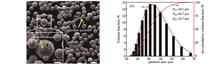
Ziwei Yang, Junqiang Xu, Shun Guo, Wendi Wu, and Qi Zhou
ObjectiveMetastable β titanium alloy has a high melting point, high activity, low thermal conductivity, and high deformation resistance. However, traditional manufacturing methods face several problems when dealing with the complex components of metastable β titanium alloys, such as numerous processes, long cycles, high cost, and low yield. Laser selective melting (SLM) is a new manufacturing technology that uses a laser as the heat source to melt metal powders layer-by-layer to manufacture solid parts. Owing to its super-complex structure forming ability, high material utilization rate, and rapid prototyping manufacturing ability, SLM provides an excellent solution for the manufacturing of titanium alloy parts with complex structures in aerospace. For the initial manufacturing process of metastable β titanium alloy, the cooling rate range of SLM is 103?108 K/s-1, while that of traditional vacuum arc melting (VAM) is 101?102 K/s-1. Non-equilibrium solidification resulting from rapid cooling is advantageous for grain refinement. The grain sizes of the SLM samples are significantly smaller than those of the VAM samples, and the grain size has a significant impact on their mechanical properties. The VAM Ti-1023 alloy is used to simulate the as-cast microstructure of a Ti-1023 alloy. The differences in the microstructures and mechanical properties of the SLM and VAM Ti-1023 alloys are compared. The effects of rapid cooling conditions on the microstructure and properties of Ti-1023 alloy are systematically studied and provide a theoretical basis for the additive manufacturing of complex components of metastable β titanium alloy.MethodsThe SLM samples are fabricated using the Ti-1023 alloy powder prepared by gas atomization through laser selective melting. Figure 1 illustrates the morphology and particle size of the Ti-1023 powder. A laser metal powder 3D printer is used to produce the SLM samples. The laser spot diameter is 70 μm, and 20 mm×20 mm×10 mm blocks are directly deposited on a commercial Ti-6Al-4V substrate as shown in Fig. 2(a). Table 1 lists the elemental contents of both the Ti-6Al-4V substrate and Ti-1023 powder. In the preparation process, a laser power of 250 W, scanning speed of 1100 mm/s, scanning spacing of 60 μm, powder thickness of 30 μm, and rotation scanning strategy of 67° are employed as illustrated in Fig. 2(b). The sample with a relative density of 99.9% can be obtained by using Archimedes method.The VAM samples are prepared on a commercial Ti-1023 alloy plate. The elemental composition of the commercial Ti-1023 alloy plate is listed in Table 1. The treated raw materials are placed in a water-cooled copper crucible in a VAM furnace. The furnace is first vacuumed to a gas pressure of 5×10⁻⁴ Pa, and then filled with argon . After three times, the ambient oxygen content is reduce to avoid sample oxidation. The surfaces of the VAM and SLM samples are then treated using a vibration-polishing equipment. The vibration-polishing frequency and polishing time are set to 56 Hz and 16 h, respectively. Next, the microstructures of the samples are observed and analyzed using an X-ray diffractometer, optical microscope, scanning electron microscope, and electron backscatter diffraction equipment. The tensile properties of the Ti-1023 samples under different processes are tested using a universal mechanical testing machine. The tensile tests are performed at room temperature at a tensile speed of 0.1 mm/min.Results and DiscussionsAs shown in Fig. 3, the phase composition of the VAM sample is α+β phases, and the SLM sample is mainly composed of β phase. It is shown that the SLM rapid cooling condition inhibits the phase transition process of β→α and a full β-phase structure forms, while the VAM sample is composed of an α+β dual phase structure. Under rapid SLM cooling, the grain size is approximately 1/10 that of VAM as shown in Fig. 4. The acicular α phase with volume fraction of 3.11% forms in the VAM sample during cooling. Simultaneously, the acicular α phase accumulates at the grain boundary of the β phase and disperses inside the β grains as shown in Fig. 8. Although the SLM sample lacks a high-hardness α phase, the high-density dislocation caused by the rapid cooling conditions is 2.1 times that of the VAM sample as shown in Fig. 7. The dislocation grid is an immovable dislocation, and its main role is to coordinate the lattice interface and maintain material continuity. Dislocation movement is hindered during the deformation process, thereby improving the yield strength of Ti-1023. The full β-phase structure of the SLM sample avoids the formation of the α/β interface and produces stress-induced martensitic transformation during deformation as shown in Fig. 9. The stress-induced martensitic transformation can increase the fracture elongation by more than five times that of the VAM sample as shown in Fig. 5.ConclusionsDuring the cooling process of VAM Ti-1023 alloy, the phase transition from β to α occurs, and the acicular α phase with volume fraction of 3.11% is produced. The microstructure at room temperature is composed of α+β phases. Because of the rapid cooling of the SLM Ti-1023 alloy, the formation of the β phase is inhibited, and the room-temperature structure is composed of single β phase.SLM samples lack a high hardness α phase and their yield strength is comparable to that of VAM samples owing to the presence of high-density dislocations, which inhibit dislocation movement under rapid cooling conditions.The full β-phase structure of the SLM sample avoids the formation of the α/β interface. As a result, stress-induced martensitic transformation occurs during deformation, leading to an increase in fracture elongation by more than five times that of the VAM samples.
Dec. 25, 2023Vol. 50 Issue 24 2402306 (2023)
Jianfeng Song, Youming Fan, Zhaoxu Jiao, Guangyao Xie, Wenwu Wang, and Yonggang Dong
ObjectiveSelective laser melting (SLM) is an additive manufacturing technology that utilizes a multi-channel overlapping process to form a single layer, followed by powder deposition and formation of multiple layers to accumulate the final part. The morphology of the single-layer multi-channel directly affects the powder deposition process and the quality of interlayer bonding and porosity in the subsequent SLM process. Additionally, owing to the heat transfer boundary conditions and thermal accumulation effects in the layer-by-layer process, there is a certain fluctuation in the width of the molten channel along the scanning direction, as well as differences in the morphology between the first and last formed melt tracks and between the surface and bottom layers. Currently, research on the quality of SLM parts mainly focuses on the final surface roughness and porosity. However, the quality and precision of SLM parts depend largely on the quality of single-channel and single-layer multi-channel formation during the manufacturing process. In this study, we investigate the SLM process and analyze the quality of single-channel and single-layer multi-channel formation. This study aims to provide insights into controlling the surface and internal quality of SLM parts.MethodsThis study employed a 316L stainless steel material. First, a powder bed model was established using the discrete element method, considering various factors such as surface tension, evaporation, recoil pressure, Marangoni effect, and gravity. A fluid dynamic model of the powder melting process was then constructed in FLUENT to simulate the process of single-channel formation in SLM. The dynamic behavior of the molten pool during the process was analyzed. Single-channel SLM experiments were designed, and the formed parts were observed and measured microscopically. The simulation and experimental results were combined to identify the optimal process parameters for achieving high-quality single-channel formation. Finally, a geometric reconstruction of the single layer multi-channel model was performed by MATLAB based on the experimental and simulation findings.Results and DiscussionsThe molten channel width and its coefficient of standard deviation of the SLM process were investigated by varying the laser power and scanning speed for 316L stainless steel powder. When the laser power is maintained at a constant 200 W, increasing the scanning speed to 2 m·s-1 results in a decrease in the molten channel width to 46.65 μm, accompanied by an increase in the coefficient of standard deviation of the molten channel width to 22.65% (Fig. 7). High-quality single-channel formation is difficult to achieve at excessive scanning speeds, as indicated by interruptions in the molten channel at scanning speeds greater than 2 m·s-1. When the laser scanning speed is maintained at 1.3 m·s-1, within the laser power range 100?300 W, the molten channel width initially increases to 69.64 μm before decreasing. Similarly, the coefficient of standard deviation initially decreases to 13.11% and then increases (Fig. 11). Notably, different molten channel widths and coefficients of standard deviation are obtained under the same line energy density, and the coefficient of standard deviation varies significantly, fluctuating between 12.26% and 22.65% (Table 4). Based on these findings, a laser power of approximately 200 W and a scanning speed of around 1.0 m·s-1 are found to be optimal for achieving high-quality single-channel formation (Fig. 15). To further analyze the molten channel morphology, a mathematical representation of the molten channel cross-section was developed, dividing the contour curve into upper and lower parts. The computed contour curve exhibits good agreement with the actual contour curve, indicating that the mathematical model accurately represents the molten channel cross-section shape (Fig. 17). Furthermore, based on this representation, a three-dimensional reconstruction of the multi-channel morphology was performed, providing a basic characterization of the single-layer multi-channel morphology (Fig. 19).ConclusionsIn this study, the SLM process of 316L stainless steel powder was investigated through a multi-field coupled simulation, experimental tests, and microscopic observations of the molten channel morphology. The results reveal that the molten channel width is inversely proportional to the scanning speed, whereas the coefficient of standard deviation is directly proportional to the scanning speed, at a constant laser power. When the scanning speed is constant, an increase in laser power initially leads to an increase in the molten channel width, followed by a decrease, whereas the coefficient of standard deviation initially decreases and then increases. The line energy density has no significant effect on the signal molten channel and its coefficient of standard deviation, it is concluded that a laser power of approximately 200 W and a scanning speed of around 1.0 m·s-1 are optimal for achieving a coefficient of standard deviation below 15%, that is, high-quality single-channel formation. Furthermore, a mathematical model based on the well-formed single molten channel cross-section and overall contour was developed, which accurately represents the molten channel shape. This model provides a new method for further research on controlling the surface roughness and porosity of SLM-formed parts.
Dec. 25, 2023Vol. 50 Issue 24 2402307 (2023)
Qianhao Wang, Hualong Zhao, Xiaojun Yang, Wenlong Wen, and Yi Li
ObjectiveThis study investigates the prevalent process problems, such as “microcracking” and “induced streaking,” in the femtosecond laser processing of hard and brittle transparent materials. The study employs the femtosecond time-resolved pump-probe shadow imaging technique to visualize the electron dynamics during the femtosecond laser multi-pulse ablation of quartz glass. Particularly, the plasma filament evolution at the early stage of laser pulse ionization (before 700 fs) is analyzed. The multi-pulse-induced microstructures distribute the filament formation regions on both sides of the microstructure with respect to the axial direction of the light pulse propagation. The distribution on both sides is primarily due to the refraction of the light pulse by the sidewalls of the microstructure, while that on the axis is caused by the difference in the shape of the bottom and sidewalls of the microstructure, creating the light range difference. The empirical results show that the pulse train induces a remodeling effect of the microstructure on the subsequent light field during multi-pulse processing, affecting the distribution of the plasma filament formation region and energy deposition—the core mechanism responsible for common process problems.MethodsA femtosecond time-resolved pump-probe shadow imaging setup was built to capture the propagation and ionization process of a single subsequent pulse beneath the microstructure induced by irradiating the material with 219 fs pulses. First, the actual spatial location of the focus was determined by imaging the shadow of the air-ionized plasma at the focus. After that, the power density at the material surface was obtained for different focus positions. The distinctive “V” and “inverted trapezoid” shapes were obtained after controlling the relative positions of the laser focus and the material. Second, the ionization process of femtosecond time-resolved propagation of the 220th pulse under different microstructures was obtained by modulating the time delay between pump and probe beams. Finally, the ionized filament-forming regions in the transient ionization images were compared with the process defects to reveal the formation mechanism of the process defects.Results and DiscussionsThe propagation and ionization process of the 220th pulse is observed using femtosecond time-resolved pump-probe shadow imaging (Figs.5.6.9.10). The physical mechanisms governing process problems such as “microcracking” in micromachining of hard and brittle materials are revealed. The light-field remodeling effect, guided by various morphology microstructures, leads to energy deposition and the mechanism of generating common process problems. In the context of multi-pulse processing, the influence of energy deposition (propagation and ionization) is determined by the linear refractive index of the material, a nonlinear refractive index that varies with the light intensity, plasma defocusing effect, microstructure morphology, and the focusing conditions in conjunction with the laser fluence on the material surface. Moreover, the relaxation time of ionized free electron number density during light field propagation is determined to be less than 300 fs across diverse microstructures.ConclusionsUnder multi-pulse irradiation, the remodeling effect of different microstructural morphologies on the subsequent light field orchestrates the nonlinear ionization process. In the case of the V-shaped structure, the formation process is accompanied by decreasing tilt angle of the sidewalls, guiding the ionization filamentation direction of the subsequent light field and sweeping across the sidewall region. It corresponds to the areas of “microcracks” and “induced stripes” on both sides of the microstructure. Conversely, the “inverted trapezoidal” structure yields strong ionization filament formation at its relatively flat bottom center region owing to the ionization effect at the bottom of the structure. For the “inverted trapezoidal” structure, a strong ionization effect occurs at the center of the relatively flat bottom, which is the root cause of the fragmentation at the bottom. Overall, the light-field remodeling effect, facilitated by different morphology microstructures, plays a crucial role in energy deposition and governing the common process problems. This result offers directions for optimizing machining processes, such as selecting the number of pulses and controlling the focal feed. Additionally, the high-temporal-resolution pump-probe shadow imaging technique holds promise for predicting fragmentation regions in different morphologies of hard and brittle transparent materials, serving as a powerful tool for online monitoring of high-end processing equipment.
Dec. 25, 2023Vol. 50 Issue 24 2402101 (2023)
Gaoyang Mi, Yiming Jiang, Chunming Wang, Mingyang Zhang, and Qiubao Ouyang
ObjectiveThe 7-series aluminum alloy is a heat-treatable aluminum alloy widely used in aerospace, rail transit, and other fields because of its excellent specific strength. Laser beam swing welding is a new method developed from conventional laser-welding technology. It can reduce the temperature gradient, stabilize the welding process, and inhibit the formation of pores and other defects in the weld. The addition of alloying elements is currently the focus of research for improving the weld performance. Many researchers worldwide have shown that adding rare-earth elements or Zr, Ti, and other elements to the weld can improve the mechanical properties. However, research on the effect of Ti addition on the microstructure and properties of 7075 aluminum alloy weld is not yet comprehensive. In this study, a systematic investigation of the effect of the thickness of a Ti metal interlayer on the microstructure and mechanical properties of 7075 aluminum alloy weld joints is reported.MethodsIn this study, 2 mm thick 7075 aluminum alloy and Ti foils of different thicknesses were used. First, welds with different thicknesses of Ti metal intermediate layers were prepared using laser beam swing welding. Then, methods, such as scanning electron microscopy (SEM), X-ray diffraction (XRD), energy-dispersive X-ray spectroscopy (EDS), and electron backscatter diffraction (EBSD), were used to analyze the effects of different Ti interlayer thicknesses on the microstructures and phases of the weld metal. Finally, by analyzing the fracture location and considering the changes in the tensile strength of the joint, the influence of adding different thicknesses of Ti metal intermediate layers on the mechanical properties of the joint was determined.Results and DiscussionsWhen the thickness of Ti intermediate layer is 0.02 mm, the Ti content in the liquid metal is relatively low. During the cooling solidification process, Al grains precipitate simultaneously with TiAl3, and the TiAl3 phase forms a short rod-shaped distribution near the interface of the aluminum grains during the solidification process. When the thickness of Ti intermediate layer is 0.03 mm, the liquid metal first precipitates a high-melting-point TiAl3 phase during the solidification process. The precipitated phase is small and cross shaped. As the temperature continues to decrease, the TiAl3 phase dispersed in the molten pool becomes the substrate for heterogeneous nucleation. When the thickness of Ti intermediate layer is 0.04 mm, excess Ti cannot be dissolved in liquid Al, and a large area of unmelted Ti is retained. At the interface between this phase and the Al grains, a short rod-shaped TiAl3 phase forms to envelop the unmelted Ti. When the thickness of the Ti intermediate layer is 0.02 mm, the influence of Ti on the fusion line is relatively small. The fusion line on both sides of the weld becomes the weak position of the welded joint owing to the reduction in alloy element segregation and the strengthening phase. When the thickness of the Ti interlayer increases to 0.03 mm, the interface between a small amount of Ti gathering area and the Al grains in the weld becomes the crack source. When the thickness of the Ti interlayer continues to increase to 0.04 mm, a large number of cracks are generated in a large area of the Ti gathering area, and these cracks continue to extend and connect with each other, resulting in joint failure.ConclusionsBy studying the effects of Ti intermediate layer thickness on the weld formation, microstructure, and mechanical properties of the weld after adding different thicknesses of Ti metal intermediate layers in 7075 aluminum alloy during laser beam swing welding, the following conclusions can be drawn.(1) With the increase in Ti intermediate layer layer thickness from 0.02 to 0.04 mm, a short rod-like TiAl3 phase, cross-shaped TiAl3 phase, and large area of Ti gathering area appear in the weld. The EBSD results indicate that the microstructure of the weld area with the addition of the Ti intermediate layer consists of fine equiaxed grains. When a 0.03 mm thick Ti intermediate layer is added, the average equivalent circular diameter of the equiaxed grain area in the weld is 3.34 μm. The weighted average value of the grain area is 1.7% of the grain size of the base material.(2) The fine TiAl3 phase is mainly distributed within the Al grains owing to the formation of the high-melting-point TiAl3 phase as the heterogeneous core of the Al grains during the solidification process and the segregation of Zn, Mg, and Cu at the grain boundaries, resulting in the formation of hard and brittle phases, such as Al2CuMg, which weakens the grain boundaries.(3) As the thickness of the intermediate Ti metal layer increases from 0.02 to 0.04 mm, the average tensile strength of the joint shows a pattern of first increasing and then decreasing. When the thickness of the Ti intermediate layer is 0.03 mm, the average tensile strength is the highest, reaching about 377.8 MPa, which is 69% of the base material strength.(4) When the thickness of the Ti intermediate layer is 0.02 mm, the weak position of the joint are located at the grain boundaries of the fusion zone and the heat-affected zone. When the thickness of the Ti intermediate layer is 0.03 mm, the weak position of the joint is in the fine equiaxed crystal zone on both sides of the weld. When the thickness of Ti interlayer is 0.04 mm, the weak position of the joint is in the Ti gathering area in the middle of the weld.
Dec. 25, 2023Vol. 50 Issue 24 2402102 (2023)
Yuqi Zhou, Lihong Chen, Jianfeng Wang, Zhu Li, Zhan Mu, and Xiaohong Zhan
ObjectiveSince the discovery of the Invar alloy by foreign scientists in the 19th century, it has been of great importance because of its extremely low coefficient of thermal expansion, which is very similar to that of composite materials. It is thus widely used as an important material for large-scale composite dies in the aerospace field. In the domestic development of Invar alloys, their thermal, physical, and mechanical properties have been the main focus of attention; however, only a few scholars have studied the welding process of domestic Invar alloys and reported results have been limited to process parameters and other aspects. Therefore, this study contrastively analyzes the microstructural differences of welded joints of 4 mm thick domestic Invar alloy obtained under different laser heat inputs and studies the effects of grain morphology, texture, and grain size in the weld seam on the tensile properties of the welded joints.MethodsThe dimensions of the welded parts used in this experiment are 100 mm×50 mm×4 mm (Fig.1). A fiber laser is used as the laser source in this experiment. After passing through the collimator and focusing mirror, the laser spot on the surface of the plate has a diameter of 0.3 mm. Scanning electron microscopy (SEM) is used to observe the microstructure of the joint cross section and the tensile fracture morphology according to the obtained tissue morphology to study the microstructural characteristics of the joints under different heat inputs. Electron backscatter diffraction (EBSD) technology is used to observe the grain size and orientation of the weld seams.Results and DiscussionsThe laser welded joint is divided into three zones weld fusion zone, base metal, and narrow heat-affected zone. There is an obvious boundary of the grain growth intersection at the center of the weld seam. As the welding heat input increases, the size of the weld cross section significantly increases (Figs.3 and 4). The weld seam is mainly composed of large columnar grains, and primary and secondary dendrites are clearly observed near the centerline of the weld seam (Fig.5). The metal solidification of an Invar alloy laser-welded joint is a rapid and directional solidification process that involves epitaxial growth on the base metal. The ratio of the temperature gradient to the cooling rate determines the degree of component undercooling, which has a significant impact on the dendritic morphology of the solidified structure (Fig.6). The grain orientation in the middle of the weld seam under a high heat input is relatively disordered and the texture strength is high, indicating that the grain competition growth mechanism is stronger than that under a low heat input. Meanwhile, the average grain area under a low heat input is refined by 29.8% compared with that under a high heat input (Fig.7). Compared to those under the high heat input, the number of sub-grains at the bottom of the weld seam increases and their size decreases under the low heat input, with an average secondary dendrite spacing of approximately 6.11 μm decreasing to approximately 4.26 μm (Fig.8). The tensile results indicate that the grain coarsening caused by increased heat input leads to a decrease in the tensile strength of welded joint from 473.4 MPa to 432.9 MPa, while the size and depth of equiaxed dimples at the fracture surface are significantly reduced (Figs.9 and 10).ConclusionsThe microstructural differences of welded joints of 4 mm thick domestic Invar alloy obtained under different laser heat inputs are contrastively analyzed, and the effect of grain size on the tensile properties of welded joints is studied. The results show that the weld seam is primarily composed of columnar dendrites, and the grain growth mode is similar under different heat inputs. However, the size of the columnar grains gradually increases with increasing heat input. The average grain area under the low-heat-input (90 J/mm) condition is 12599.7 μm2, refined by 29.8% compared to that under the high heat input (200 J/mm), and the number of sub-grains at the bottom of the weld seam increases and the size decreases under the low heat input, with an average secondary dendrite spacing of approximately 6.11 μm decreasing to approximately 4.26 μm. The tensile results indicate that the grain coarsening caused by increased heat input leads to a decrease in the tensile strength of the welded joint from 473.4 MPa to 432.9 MPa, while the size and depth of equiaxed dimples at the fracture surface are significantly reduced.The growth of columnar grains in the weld seam is limited due to the fast-cooling rate under the low heat input (90 J/mm), resulting in relatively small grain sizes. Under the high heat input (200 J/mm), due to the Marangoni convective flow in the molten pool, the weld cross section presents an X-shaped shape and causes a significant increase in cross-sectional size. At the same time, the highest temperature experienced by the liquid molten pool gradually increases, leading to grain boundary migration and grain coarsening, resulting in a gradual increase in the size of columnar grain.With an increase in welding heat input, a small amount of fine equiaxed sub-grain structure appears near the centerline of the weld seam. Compared to that under the high heat input, the competitive growth degree of grains under the low heat input is relatively weak, and the average grain area of the weld seam has also been refined by 29.8%. At the same time, the number of equiaxed sub-grain structures at the bottom of weld seam increases, the size decreases, and the average secondary dendrite spacing near the centerline of the weld is only about 5.12 μm, which is 0.99 μm less than that under high heat input.The morphology and size of grains can affect the stress-strain distribution in local areas of the welded joint, thereby affecting the strength and plasticity of the welded joint. The tensile strength of the welded joint decreases from 473.4 MPa to 432.9 MPa, and the elongation decreases from 20.7% to 15.3%. The fracture morphology of the welded joint indicates that the size and depth of equiaxed dimples gradually decrease with increasing heat input.
Dec. 25, 2023Vol. 50 Issue 24 2402103 (2023)
Xiaohu Hao, Geng Xu, Zeqin Cui, Zhengxiang Ding, Yingjie Shi, Wenxian Wang, and Weiguo Li
ObjectiveThe limited solid solubility between aluminum (Al) and copper (Cu) leads to the formation of massive brittle intermetallic compounds in the resultant Al/Cu dissimilar joints, increasing crack sensitivity and decreasing mechanical properties. High-quality aluminum/copper joining in power batteries is a key process to ensure the battery module works efficiently. However, owing to the high reflectivity of a regular laser on a nonferrous metal surface, the laser power threshold is high, and it is difficult to control the formation of brittle intermetallic compounds. In this study, a blue-red composite laser is used to produce an aluminum/copper hybrid structure, and the effects of the welding speed on the microstructural, tensile, and electrical properties of the joint are studied.MethodsA 1050 aluminum plate with 0.5 mm thickness and a T2 copper plate with 1 mm thickness are used in this experiment. The surfaces of the test pieces are roughened and cleaned with ethanol before welding. The blue-red composite laser is modulated by the superposition of two circular uniform laser beams with different spot diameters. Welding is conducted using high-purity argon gas at a flow rate of 15 L/min. The aluminum plate is lapped on the copper, and the lap width is maintained constant at 20 mm. An electrical discharge wire-cutting machine is used to manufacture metallurgical and tensile specimens. The metallographic specimens are inlaid with an epoxy resin, sandpapered to smooth surfaces, and polished for metallographic observation.The microstructural morphology and chemical composition of the feature phases are examined by scanning electron microscope (SEM) and energy dispersive spectroscopy (EDS). Tensile tests are performed under different welding speeds (V) using a universal testing machine. Three specimens are tested, and the average fracture loads are calculated. The fracture paths and surface morphologies are examined. The contact electric resistance is measured using a direct current power supply and a digital multimeter.Results and DiscussionsWith increasing welding speed, the melting widths of 1050 aluminum and T2 copper decrease gradually. The melting width of 1050 aluminum is larger than that of T2 copper. At V=100 mm/s, the metal at the copper side is only fused slightly with a depth of 52 μm. At V=60 mm/s, the weld is in good shape, and the edges and center of the aluminum side are mainly composed of α-Al solid solution, and no obvious continuously distributed brittle phases are formed. The overall morphologies of the weld are similar under different welding speeds. The Al-side weld seam mainly consists of Al solid solution interspersed with a portion of the Al-Cu subeutectic phase mesh structure (Fig. 4). The weld fracture load increases first and then decreases steadily with an increase in the welding speed, and the maximum fracture load of the specimen reaches 571.5 N under the condition of V=60 mm/s. At different welding speeds, the Al/Cu composite laser-welded joints fracture at the Al/Cu interface, and the primary fracture is cleavage fracture. At V=60 mm/s, resistance values can be as small as 89 μΩ. At a low welding speed, the interface is prone to cracking, leading to deterioration of the joint conductivity. However, at higher welding speeds, the melt pool exists for a short period, and the melt width and joining area decrease, resulting in an increase in the electrical resistance.ConclusionsIn this study, the lap welding of 1050 Al and T2 Cu is achieved using a blue-red composite laser. A welding speed in the range of 60?100 mm/s can yield aluminum/copper joints with flat surfaces and good connection quality. When the welding speed is less than 40 mm/s, the spatter and melt-through holes are formed on the weld surface, which deteriorates the welding quality. From top to bottom, the weld microstructures consists of the Al solid solution, Al solid solution + Al-Cu eutectic, and Al2Cu phases. Owing to the increase in the welding speed, the existence time of the molten pool is shortened, the diffusion of Cu is limited, and many Al-Cu eutectic compounds accumulate at the Al/Cu interface. The maximum fracture load of the Al/Cu joint is 571.5 N at the welding speed of 60 mm/s, and the fracture is cleavage fracture. The aluminum/copper contact resistance reaches a minimum of 89 μΩ at the welding speed of 60 mm/s. Welding speeds that are too high or too low tend to aggregate compounds and reduce conductivity.
Dec. 25, 2023Vol. 50 Issue 24 2402104 (2023)
Libo Wang, Xiuquan Ma, and Zhengwu Zhu
ObjectiveAluminum alloys are vital materials for performance improvement and structural weight reduction in automotive, aerospace, and other industries, owing to their high specific strength, corrosion resistance, and low density. However, the physical properties of aluminum alloys, including their high reflectivity, low boiling point, and high coefficient of thermal expansion, have resulted in problems such as low energy utilization, high porosity, and poor weld seam formation in laser welding. With the rapid development of galvanometer scanning technology, the combination of laser technology with galvanometer mirrors, known as laser stir welding, has emerged as a solution to these problems. By investigating the shape of the stirring motion, stirring patterns, and beam diameter during the welding process, researchers have explored effective approaches for achieving high-quality aluminum alloy formation. Nonetheless, challenges persist, including the expansion of the weld pool diameter and the reduction in pool depth, which directly affect the quality of the weld formation. Therefore, to address the low energy utilization (resulting in shallow melting penetration and a large melting width) observed in laser stir welding and to examine the influence of a small spot generated by collimating and focusing a small-core-diameter laser on the weld formation quality of aluminum alloys, this study investigates the aluminum alloy welding seam formation under different welding process parameters with 2-mm-thick 2A12 aluminum alloy as the research object.MethodsBefore welding, the surface of the test specimen is prepared by grinding with a steel wire brush to remove the surface oxide film. Subsequently, the surface is wiped with an acetone solution to eliminate any oil contamination. The 2A12 aluminum alloy is subjected to laser stir welding in a flat-plate configuration, and the circular motion of the laser beam is achieved using a two-dimensional galvanometer. After welding, the surface morphology of the welds is examined using a metallographic microscope. Metallographic samples are prepared along the vertical direction of the weld. The metallographic samples are embedded, ground, and polished, followed by corrosion using Kroll's solution (1 mL HF+1.5 mL HCl+2.5 mL HNO3+95 mL H2O). Finally, the weld microstructure is observed using a field-emission scanning electron microscope.Results and DiscussionsTrajectory simulation and energy distribution calculations are conducted using MATLAB. The results indicate that a higher energy density is achieved with a 14-μm-core-diameter laser at low power, enabling deeper weld penetration. The depth-to-width ratio of the weld pool is significantly affected (Figs.3 and 4). Within the stirring frequency range 50?200 Hz, the laser energy gradually shifts from one side to the other as the stirring frequency increases, eventually resulting in dual-energy peaks on both sides. As the stirring frequency increases to 300 Hz, the laser energy is concentrated in the middle region (Figs.5 and 6). The welding process is observed using a high-speed camera (Fig.7), which reveals that increasing the stirring frequency not only reduces the peak energy density but also facilitates a more uniform energy distribution, improving the stability of keyhole formation and enhancing the quality of the weld. The investigation of the threshold for deep penetration keyhole formation demonstrates that the threshold for a 14-μm-core-diameter laser is 19.1 times higher than that of a conventional 100-μm-core-diameter laser and 54.0 times higher than that of a 200-μm-core-diameter laser. This effectively prevents the transition from deep penetration welding to heat conduction welding, thereby maintaining a nearly constant weld width and depth (Fig.8).ConclusionsIn the present study, the impact of the trajectory and energy density of a 14-μm-core-diameter laser on weld formation is investigated. The results reveal that the laser with a smaller core diameter exhibits a smaller spot size and a higher concentration of energy during the stirring-welding process. It has a greater threshold for keyhole formation, resulting in a consistent depth-to-width ratio of 0.68 and a weld area of 2.1 mm2. The laser energy peak underwent a transition from a single peak to a double peak and ultimately converges in the central region. An increase in the stirring frequency within the range of 50?200 Hz is found to contribute to a more uniform distribution of laser energy, a reduction in spatter defects during the welding process, and an improvement in the stability of keyhole formation. At the stirring frequency of 200 Hz, the weld exhibits stable fish-scale patterns without visible defects or significant porosity.
Dec. 25, 2023Vol. 50 Issue 24 2402105 (2023)
Wang Cai, Ping Jiang, Leshi Shu, Shaoning Geng, Qi Zhou, and Longchao Cao
ObjectiveThe process stability of high-power laser welding of stainless steel plates is affected by the processing environment, assembly state, and other factors that are prone to spatter defects. The formation of a large amount of spatter can lead to a reduction in the molten metal in the weld. This affects the service performance of the weld seam and leads to safety hazards. Additionally, the removal of the solidification spatter from the weld plate requires additional processing procedures and affects the efficiency of the component production. In recent years, the technology for real-time monitoring and control of the welding process has emerged as a leading-edge discipline and a research hotspot, offering broad application prospects. This technology can accurately sense the state of the welding process and control the process parameters to suppress defect generation based on real-time feedback operation from the sensed information, which is the key to guaranteeing the stability of the welding process and improving the welding quality. Therefore, accurate and rapid monitoring of spatter is the basis for solving spatter defects and improving the production efficiency of components.MethodsIn this study, a machine vision-based spatter monitoring method is proposed for obtaining dynamic spatter features to analyze weld quality. First, laser welding is performed on an 8-mm thick 316 L stainless steel plate using a welding system comprising of a 30-kW fiber laser. The laser powers in different areas of the weld plate are 6, 7, and 8 kW. The welding speed is 40 mm/s and shielding gas flow rate is 30 L/min. The laser-head tilt angle and defocus distance are 10° and 0, respectively. A high-speed camera with a sampling frequency of 11000 frame/s and resolution of 640 pixel×480 pixel is used to observe the formation and motion of the spatters. Subsequently, a spatter-identification method based on multithreshold segmentation, shape recognition, and image fusion is proposed to extract the spatter center coordinates, sizes, and velocity features. Finally, a spatter trajectory reconstruction method is proposed to obtain the spatter trajectory and quantitative characteristics to analyze the dynamic behavior of the spatter and its influence on weld quality.Results and DiscussionsSpatters in high-power laser welding are observed using a macrolens high-speed camera (Fig.3). The metal vapor morphology and intensity constantly change, affecting the spatter observations. To monitor spatter accurately, an image processing method based on multithreshold segmentation, shape recognition, and image fusion is proposed (Fig.4). The spatters are accurately recognized (Fig.5), and a neighboring image fusion method is proposed to remove the residual strong metal vapor interference (Fig.6). The center coordinates, sizes, and velocity features of the spatter are extracted and analyzed, and the velocity of the spatter in the monitoring image is decomposed along horizontal and vertical directions (Fig.7 and Table 2). Spatters exhibit minimal movement (less than one pixel per image) in the monitoring images obtained at this high monitoring frequency and are essentially of the same size and location in neighboring monitoring images. A spatter motion trajectory reconstruction method based on continuous spatter recognition image fusion and a spatter size reduction method based on mask image fusion are proposed (Figs.8 and 9). The methods accurately reconstruct all the spatter motion trajectories in the sampling interval and accurately extract the spatter quantity features based on the spatter trajectories (Fig.10). The spatter is nearly spherical because of the surface tension, and the spatter projection area reflects the spatter size (Fig.11). The spatter trajectory resembles a parabola. The velocity in the horizontal direction is nearly uniform, whereas that in the vertical direction gradually decreases (Tables 3, 4, and 5). The numbers of spatters in the sampling area at laser powers of 6, 7, and 8 kW are 78, 124, and 43, respectively (Fig.12). It can be observed that when the weld is partially penetrated, the laser power and number of spatters increase. When the weld is excessively penetrated, several metal vapor and spatters are ejected from the bottom of the keyhole, and the number of spatters decreases significantly (Fig.13).ConclusionsIn this study, a motion spatter monitoring method for a stainless steel high-power laser welding process is investigated based on machine vision technology. The main conclusions are as follows:1) A spatter-recognition method and a strong metal vapor interference removal method are proposed to accurately recognize the spatter and extract its size and speed features.2) Spatter motion trajectory reconstruction and spatter size reduction methods are proposed to extract spatter quantity features accurately.3) The speed in the horizontal direction is nearly uniform, and the speed in the vertical direction gradually decreases. The spatter trajectory resembles a parabola.4) When the weld is partially penetrated, the laser power increases and the number of spatters increases. When the weld is excessively penetrated, some metal vapor and spatters are ejected from the bottom of the keyhole and the number of spatters decreases significantly.
Dec. 25, 2023Vol. 50 Issue 24 2402106 (2023)
Yaqing Qiao, Aiguo Tang, Tianting Chen, Haoran Ma, Yi Liu, Hui Gao, Wei Xiong, and Leimin Deng
ObjectiveProcessing blind holes in FR4 copper-clad boards to interconnect electronic components is an essential method in printing circuit boards. The quality of blind hole manufacturing is a crucial factor in determining device performance. Laser processing offers advantages such as high precision, no mechanical force, and flexible control, making it the primary method for machining blind holes in FR4 copper-clad boards. Recently, the application of ultrashort pulse lasers has reduced the thermal effects and improved drilling accuracy. However, current laser processing techniques still face challenges in controlling the taper of hole sidewalls and achieving sufficient hole depth. Sidewall taper is a crucial indicator for evaluating blind holes. To ensure reliable interlayer connections, the solder pad at the bottom of the blind hole should be exposed as much as possible. On the other hand, blind holes with uniformly inclined and smooth sidewalls are more conducive to subsequent metallization processes, thus improving the yield of finished products. Considering these conflicting requirements, the ratio of the bottom diameter to the top diameter of blind holes must be controlled within the range of 70%?90%. Furthermore, existing research primarily focuses on shallow blind holes, and the manufacturing of deep blind holes with depths exceeding 500 μm still presents significant challenges. In this study, we adopt five-axis laser scanning technology to avoid obstruction of the laser beam by the material surface and sidewalls in order to achieve sidewall taper adjustment and improve blind hole depth.MethodsIn this study, a five-axis laser scanning system with a wavelength of 1030 nm and a pulse width of 436 fs is employed to perform laser scanning. The experimental material is an FR4 copper-clad board, with the glass fiber composite material thickness of 925 μm and the copper thickness of 35 μm. The processing of blind holes adopts a layer-by-layer material removal method. The processing of each layer is divided into two steps. In step 1, the laser draws a spiral line on the material surface, and in step 2, the laser performs additional scanning around the hole circumference to increase the material removal rate at the sidewalls. Simultaneously, during the laser scanning of the two-dimensional pattern, the five-axis scanning system controls the tilt angle of the laser beam to avoid obstruction of laser energy by the hole sidewalls. After the scanning is completed for one layer, the laser focus moves downward to process the next layer of material until the blind hole processing is finished. Compressed air at a pressure of 1 bar(1 bar=105 Pa) is supplied coaxially. The processed results are observed using a laser confocal microscope.Results and DiscussionsCompared to laser repetition rate and scanning speed, the impact of laser pulse energy on the sidewall taper is more significant (Fig. 2). Modifying the line spacing of the spiral pattern can enhance the uniformity of material removal at the bottom of the hole and mitigate the influence of material anisotropy on the uniformity of material removal (Fig. 3). By adjusting the scanning strategy, continuous control over the sidewall taper and hole geometry dimensions can be achieved (Figs. 4 and 5). The hole sidewalls are straight with surface roughness (Sa) of less than 5 μm. The glass fiber composite material at the bottom of the blind hole is thoroughly removed, with a bottom roughness of less than 2 μm and good roundness. The damage depth to the copper layer at the bottom of the blind hole is less than 1 μm (Fig. 6).ConclusionsThis study investigates the femtosecond laser machining technology for deep blind holes in FR4 copper-clad boards using a five-axis laser scanning system. The research demonstrates that, compared with laser repetition rate and scanning speed, the variation in laser pulse energy has the most significant impact on the sidewall taper of blind holes. Matching the line spacing of the scanning pattern with laser processing parameters can improve the uniformity of material removal inside the holes. By adjusting the laser scanning strategy, the sidewall taper of blind holes can be controlled, allowing for continuous and adjustable diameter ratios between the bottom and entrance of the blind hole within the range of 70%?90%. It also enables the adjustment of the blind hole radius, with a maximum aspect ratio of 4.9∶1. Inspection of the drilling results at the bottom of the blind hole reveals complete removal of the glass fiber composite material, with a copper layer damage depth below 1 μm. This research achieves high-precision manufacturing of deep blind holes in FR4 copper-clad boards and continuous control of sidewall taper, enhancing the quality of blind hole machining and promoting the application and development of five-axis laser scanning technology.
Dec. 25, 2023Vol. 50 Issue 24 2402401 (2023)
Chen Xie, Shixian Sun, Erse Jia, and Minglie Hu
ObjectiveMicro-helices are applied in microrobots and chiral metamaterials and require various features for structure fabrication in diverse applications. The femtosecond laser direct writing (FsLDW) technology can fabricate three dimensional (3D) microstructures based on two-photon polymerization (2PP) with sub-diffraction-limited resolution. This technology is used to fabricate micro-helix structures using the widely used point-by-point writing scheme with a single focus. However, this is relatively inefficient because of the repetitive scans along many helical trajectories in the fabrication process. Recently, one-step exposure with structured light has allowed the rapid fabrication of micro-helices, wherein helical beams are specially designed with vortex phases. However, state-of-the-art schemes can only produce microstructures with limited patterns owing to the complex and professional light manipulation techniques. To efficiently fabricate micro-helix structures with flexible features such as diameter, thread number, pitch, and chirality, we propose a scheme based on dynamic multi-focus patterns to fabricate multiple helical microstructures.MethodsMicro-helix structures were fabricated by piling up the multi-focal voxels along helical trajectories. The helical motion of the voxels was divided into two components: a circular motion manipulated by dynamic holograms loaded on the spatial light modulator (SLM), and a linear motion controlled by a z-axis translation stage (Fig. 3). Based on our in-house fabrication system, we adapted the Gerchberg-Saxton (G-S) algorithm to compute dynamic multi-focus holograms on the SLM iteratively. Subsequently, the tightly focused femtosecond multi-focal beam patterns induced polymerization of the photoresist (SU-8). In this method, the diameter and thread number of the micro-helices were determined by the parameters of the hologram alone under fixed exposure conditions. The dynamic holograms with the z-axis translation stage allowed flexible control of the pitch and chirality.Results and DiscussionsThe improved G-S algorithm adapted in our setup generates a well-defined multi-focus in the experiments, showing good consistency with the simulation (Fig. 2). These multi-focused beam patterns allow the flexible fabrication of various micro-helices by piling up the multi-focus voxels in a single helical motion (Fig. 3). Using a four-focus beam as an example, the geometric features of the corresponding voxels in 2PP are experimentally characterized in terms of their diameters and axial sizes (Fig. 4). In this experiment, the threshold power is determined as 0.01 mW for every single focus under 5 ms exposure time. Micro-helices are fabricated under the aforementioned exposure conditions. However, insufficient adhesion leads to the detachment of these microstructures with high aspect ratios from the silicon substrates (Fig. 5). To address this issue, another polymerized thin film is deposited on the substrate, which is cured using a UV lamp before proceeding with 2PP. This process significantly enhances the adhesion between the microstructures and substrate. Additionally, the capillary forces occurring during the developing step of post-processing distort the microstructures by pulling down the helical threads (Fig. 5). This issue is resolved by drying the micro-helices in supercritical carbon dioxide. Finally, five sets of dynamic multi-focus holograms are used to fabricate the micro-helices with different features (Fig. 6). The spiral diameter of these microhelices ranges from 2.4 to 19.2 μm as the number of threads increases from one to eight, with adjustable chirality and pitch. Introducing supporting micro-ribs also significantly enhances the stiffness of the micro-helices, which enables the height of the micro-helices to be up to 30 μm (Fig. 7). A possible reason for the different thread widths under different pitches in the voxel-stacking model is analyzed (Fig. 8).ConclusionsIn this paper, we propose a dynamic hologram scheme to fabricate micro-helices using 2PP. In our scheme, the helical motion of the focus in conventional direct laser writing can be divided into linear and circular motions. Linear axial motion is controlled by a mechanical translation stage, and circular motion is manipulated by a set of dynamically programmable holograms. We also prove that the improved G-S algorithm is effective in generating multi-focus femtosecond laser patterns with flexibly controlled parameters to achieve circular motion. Therefore, well-defined dynamic multi-focus patterns in combination with axial mechanical motion can allow the fabrication of micro-helices with flexible control over diameters, thread numbers, pitches, and chiralities. Compared with the FsLDW method based on the single focus, the multi-focus parallel writing scheme can increase the fabrication efficiency by N times for micro-helices with N threads. Additionally, this hologram-based scheme offers advantages in terms of system cost, as it eliminates the need for an expensive motion controller for sophisticated spiral mechanical movements. The proposed flexible and economical method of micro-helix fabrication holds great potential for various applications, such as microrobots, chiral metamaterials, and bioengineering.
Dec. 25, 2023Vol. 50 Issue 24 2402402 (2023)
Pin Zhang, Yaqing Qiao, Xiaohui Su, Hui Gao, Wei Xiong, and Leimin Deng
ObjectiveGlass fiber-reinforced composite plates (GFRP) possess several advantageous properties, such as wear resistance, corrosion resistance, a high strength-to-weight ratio, and high fracture toughness. Hence, they have found extensive applications in the aviation, automotive, shipbuilding, and chemical industries. However, the distinctive structure of GFRP results in significant challenges during drilling processes, particularly when aiming for high-quality holes. Mechanical and water jet drilling methods often introduce defects, such as delamination and fiber pull-out. Hence, laser processing has emerged as a viable alternative. It eliminates the interaction forces between the laser and material owing to being a noncontact method, effectively avoiding the aforementioned defects. Consequently, it has proven to be an effective method for drilling GFRP. However, laser punching drilling and two-axis laser scanning drilling suffer from limited laser control flexibility and difficulties in eliminating sidewall tapering. Moreover, laser punching drilling is only suitable for processing small circular holes. Although laser rotary cutting and five-axis laser drilling can adjust the laser angle-of-incidence and eliminate sidewall taper, their maximum processing diameter does not exceed 5 mm, limiting the drilling of larger holes. This study proposes a four-axis laser scanning processing technique based on a dual galvanometer system. The proposed technique successfully eliminates sidewall tapering and expands the range of hole diameters that can be processed.MethodsThis study used two galvanometers to construct a four-axis laser scanning system, enabling four-axis laser scanning through a correspondence between the four-axis coordinates of the laser focus and deflection angles of the galvanometer mirrors. The experimental material was a 3.6 mm thick GFRP. The laser employed in the experiment had a pulse width and wavelength of 436 fs and 1030 nm, respectively. Following its passage through the four-axis laser-scanning system, the laser was focused onto the workpiece surface using an F-theta lens. The GFRP specimen was placed on an electric Z-axis stage. Laser drilling was performed using a layer-by-layer scanning approach, where the scanning path of the laser in the X-Y plane consisted of concentric circles. Additionally, the laser angle-of-incidence gradually increased with the scanning radius to prevent the sidewall from obstructing the laser energy. After removing each material layer, the electric Z-axis elevated the workpiece, aligning the laser focus with the next layer. This iterative process continued until the desired drilling depth was achieved. Subsequently, the optical morphology of the drilled holes was examined using a stereomicroscope. The microstructure of the sidewall was analyzed using a scanning electron microscope. Furthermore, the 3D morphology and surface roughness (Sa) of the sidewall were measured using laser confocal microscopy. The roughness measurement encompassed a rectangular sampling area of 1 mm×1 mm.Results and DiscussionsThe low laser pulse overlap rate at the sidewall affects the material removal rate, resulting in the accumulation of sidewall taper. Several improvements are observed by gradually increasing the laser angle-of-incidence from 3° to 7°. First, the laser spot size at the sidewall reduces, increasing laser energy density. Consequently, the sidewall taper decreases from 4.16° to 0.65°. However, increasing the laser angle-of-incidence does not eliminate sidewall tapering. The edge compensation scanning method can further enhance the material removal rate at the sidewall, ultimately eliminating the sidewall taper. Application of the method significantly decreases the sidewall taper to 0.24° at the laser angle-of-incidence of 3°. Similarly, the sidewall tapering reaches -0.14° at the laser angle-of-incidence of 4°. The aforementioned results are considered to successfully fabricate a circular hole with a diameter of up to 10 mm on a 3.6 mm thick GFRP specimen. Notably, the width of the heat-affected zone at the entrance and exit of the hole is less than 10 μm. Additionally, the hole sidewall exhibits a smooth surface with a surface roughness of less than 2 μm.ConclusionsThis study proposes a dual-galvanometer laser scanning processing system and develops a mathematical model to establish the relationship between mirror angles and laser scanning paths, enabling four-axis coordinated laser scanning. Laser-drilling GFRG experiments are conducted using a dual-galvanometer laser scanning processing system. The results show that the material removal rate at the scanning edges is lower than that at the central region owing to the weak overlap of the laser spots. Increasing the laser incident angle can improve the material removal efficiency at the sidewalls and reduce the sidewall taper. An edge-compensation scanning method is proposed to reduce sidewall taper. A vertical sidewall is processed at a laser angle-of-incidence of 3.7°. The processing results demonstrate consistent geometric dimensions at the entrance and exit of holes. Specifically, the hole diameter is measured to be 10 mm, and the width of the heat-affected zone is less than 10 μm. Moreover, sidewalls do not have defects, such as material delamination and fiber pull-out. Furthermore, the sidewall roughness is less than 2 μm. This study proposes a novel four-axis laser scanning method that enhances the manufacturing capability and quality of holes in GFRP, offering substantial potential for valuable industrial applications.
Dec. 25, 2023Vol. 50 Issue 24 2402403 (2023)
Chunyan Dong, Xiaoyu Zhang, Dehua Gu, Siwu Shao, Jinlong Liu, Liangxian Chen, Chengming Li, and Junjun Wei
ObjectiveDiamond has high chemical stability, mechanical properties, high carrier mobility, and thermal conductivity, which has broad application prospects in many frontier fields. Diamond with micropores has good application prospects in high-precision lead forming and high-power microwave device heat dissipation. This study established the variation law of diamond hole patterns and defect characteristics under different laser powers. The diamond hole patterns and defect characteristics are vital in implementing the heat dissipation currently used in substrates for high-frequency electronics. The basic conditions can only be provided for the subsequent microporous metallization when the pore type meets the requirements, and the surface graphite residue and the pore wall are smooth.MethodsIn this study, laser technology was used to process micropores on self-supporting polycrystalline diamond films. By adjusting the laser power, the influence of laser power on diamond microporous molding was studied, the reaction mechanism of laser-diamond interaction was discussed, and the removal mechanism of diamond was analyzed. Field emission environment scanning electron microscopy was used for morphology analysis. Laser confocal scanning microscopy was used to measure microwell contours. Laser Raman spectroscopy and X-ray photoelectron spectroscopy were used for surface composition characterization to analyze the influence of laser power on the outer and inner surface of micropores and the causes of defects. The material removal mechanism and microhole forming process during laser microhole processing were revealed by introducing diamond ablation threshold analysis.Results and DiscussionsMorphology analysis was conducted by field emission environment scanning electron microscopy, and the results showed that the microporous surface had significant sedimentary layers and spherical deposits. When the power reaches 17.6 W, the surface of the micropores is damaged and fractured, and there is an obvious stripe structure at the fracture location, which may be formed by the interconnection of crack propagation caused by thermal stress. The diamond-layered deposits begin to fall off when the microporous surface sedimentary layer is partially detached during the fracture of the diamond surface layer [Fig. 1(d)], and the thermal stress on the microporous surface is greater than the van der Waals force between the sedimentary layer and the diamond. In contrast, as the laser power increases, the thickness of the sediment layer on the diamond surface also increases, which may also be another cause of layered sediment shedding due to the difference in thermal expansion between the layered deposit and the diamond substrate. The topography of the inner surface of the micropores (Fig. 3) shows that a fine graphite layer covers the top of the micropores, and the graphite layer reduced from top to bottom. Simultaneously, significant cracks and flaky shedding of the inner surface can be observed. The microwell profile was measured by laser confocal scanning microscopy, and further analysis of the change of micropore taper showed that the inner surface of the upper end of the micropores was rough. The microporous taper decreased with the increase of laser power. In the downward energy transfer process, it is absorbed by the diamond and generates graphite. The energy received at the lower end of the micropores is reduced, and the diamond micropores finally take on a cone shape. Moreover, because the degree of graphitization increases with the increase of laser power, the thickness of the graphite layer on the surface and inner surface of the diamond increases, which improves the absorption of laser energy; hence, at high power, the energy difference between the upper and lower ends of the micropores increases, which in turn leads to an increase in taper.Laser Raman spectroscopy and X-ray photoelectron spectroscopy were used to characterize the surface composition, and it was proved that the main components of the surface and inner surface sedimentary layers of diamond after laser processing were graphite and then proved that the diamond underwent phase transition under the action of the laser. The effect of power on stress was analyzed by Raman spectral peak shift calculation. With the increase of laser power, the compressive stress on the diamond's outer surface and inner surface increases, and the amplitude of the increase is the same. Finally, introducing diamond ablation threshold analysis reveals the material removal mechanism and micropore forming process in laser microporous processing. The ablation threshold of polycrystalline diamond is 3.16 J/cm2, and the corresponding average power is 2.23 W. A phase change reaction begins on the diamond surface when the laser energy is above the ablation threshold. The increase in laser power provides more energy for the phase change reaction, and the amount of diamond removal increases, which produces more defects. The reaction is terminated when the energy is absorbed below the ablation threshold.ConclusionsThe results show that the outer surface of the micropore is damaged when the laser power is high, and the micropore's inner surface also has a striped structure. The degree of graphitization on the outer surface and inner micropore surface increased with the laser power. The taper of the microporous type decreases with the increase of laser power, and the verticality of the micropores was improved. The stress on the inner surface of the micropore during laser processing is greater than that on the edge position of the micropore.
Dec. 25, 2023Vol. 50 Issue 24 2402404 (2023)
Ying Li, Xinyue Li, Jiaqi Wang, Jinkai Xu, and Huadong Yu
ObjectiveWaterjet-assisted laser processing technology provides a new direction in the development of laser processing that can effectively mitigate thermal damage to materials during laser processing; thus, it has good prospect for microfabrication applications. During processing, the quality of the material surface can be inspected in real time, and the introduction of microscopic systems can provide a more convenient observation of material processing details as well as improve the corresponding efficiency. However, because of the interference of the waterjet, bubbles are present in the source image captured by the CCD camera, obscuring detailed information and blurring the surface. In addition, the source image sequence is only partially focused because of the limited depth-of-field of the microscope system. To enhance the detail of surface features of materials for the purpose of dehazing, an image processing technique is employed to improve the contrast of an image by emphasizing the respective brightness, saturation, and textural features of local areas. However, conventional dehazing algorithms begin with the image itself. Without considering that the local area processing method has problems including loss of detailed information and excessive contrast enhancement, development of an image dehazing method for the local areas of different images is necessary. In the traditional microscope mode, the effect of extending the depth-of-field can be achieved via component deformation; however, this has reduced efficiency, large equipment size, and low lateral resolution. Currently, image fusion based on the transform domain is a popular research topic, and is one of the most widely used and mature methods in practical applications.MethodsThis study solves the problems of waterjet interference and image fusion. Bubbles were maximally reduced via foreground segmentation and morphological theory, and the detailed information of the source images was enhanced according to the adaptive multiscale Retinex dehazing algorithm. After dividing the image into blocks, the detail index is defined by the standard deviation value of each block. The most suitable Gaussian filter function scale value was determined, and the corresponding weights were calculated to linearly superimpose the single-scale Retinex algorithm of different scales. The source image was decomposed into detail and approximate components using discrete wavelet transform, the detail component was stretched according to the human vision principle, and each discrete wavelet inverse transform was performed according to the fusion rules. As a result, a full-focus image with an extended depth-of-field can be realized.Results and DiscussionsThe experimental system adopted in this work was set up as depicted in Fig. 1, mainly constituting a laser processing and image capture system, and a high-pressure waterjet assist system. The processing and image capture system comprises a laser, waterjet nozzle, and CCD camera. The processed material surface images of the waterjet interference problem are presented in Fig. 5: (a) displays one of the source images captured in the waterjet environment and (b) shows the final processed image. The interference of bubbles on the image information in the processed image appears to fade, and more detailed features are restored. Compared with the source image, the average gradient (AG), standard deviation (SD), and spatial frequency (SF) of the processed image improved by 27.6%, 20.1%, and 4.74%, respectively. Table 3 presents the image quality comparison results of the three source images in the air and waterjet environments. In the waterjet environment, the image quality was significantly lower than that in the air environment, where the SF and AG were reduced by 33.88% and 31.11%, respectively. Figure 6 shows the source images of the material surface collected for waterjet nozzle diameters of 0.4, 0.8, and 1.2 mm as well as the processed images after algorithmic processing. As the diameter of the waterjet nozzle increases, the thicker the flowing water layer on the surface of the sample, and the more limited the image information that can be obtained from the source image. According to Fig. 7(b), the three indicators of the processed image obtained with the diameter nozzle of 0.4 mm reached 95.41%, 71.88%, and 67.29%, respectively. Fig. 8 displays the source images of the material surface collected for waterjet inclination angles of 30°, 45°, and 60°, besides the processed images after algorithmic processing. As the waterjet inclination angle decreases, the thicker the flowing water layer on the surface of the sample, the more limited the image information that can be obtained from the source image. As shown in Fig. 9(b), the three indicators of the processed image considering the 45° angle reached 90.59%,72.69%, and 94.50%, respectively; thus, maximizing the exclusion of the interference of the waterjet, which could restore part of the detailed features.ConclusionsIn waterjet-assisted laser processing, microscopic images of material surfaces are subject to waterjet interference and depth-of-field limitations. Therefore, we propose a waterjet laser processing image-fusion algorithm based on the Retinex dehazing algorithm. The method determines different Gaussian filter function scales for various images, improves the dehazing effect of traditional algorithms, and stretches the detailed components according to human vision. As a result, detail of source image information was enhanced and the image quality was improved. Experiments demonstrate that the algorithm reduces the interference of the waterjet in the source image, enhances the detailed information of the image, and achieves full focus. As the diameter of the waterjet nozzle increases and the inclination angle decreases, the water film on the surface of the material becomes thicker, and the quality of the source image is subsequently reduced, which is difficult for the algorithm to process. However, the experimental results show that with the nozzle diameter of 1.2 mm or an inclination angle of 30°, the processed image still presents most of the detailed features and improved image quality. Thus, the developed algorithm can effectively improve the efficiency of waterjet-assisted laser processing and is expected to be widely used in liquid-assisted laser processing.
Dec. 25, 2023Vol. 50 Issue 24 2402201 (2023)
Yiming Chi, Dahu Qian, Zhehe Yao, Qunli Zhang, Yunfeng Liu, and Jianhua Yao
ObjectiveThe low hardness and poor wear resistance of aluminum materials greatly limit their use in wear environments. Preparing coatings of particle-reinforced aluminum matrix composites (AMCs) by the laser alloying process can effectively improve their surface properties while maintaining their bulk advantage. However, large differences in physical and chemical properties and the low wettability between the particle reinforcements and aluminum melt cause significant stress concentration and plastic deformation at the interface, resulting in serious defects. To further improve the properties, in-situ synthesized TiB2-TiC particle-reinforced AMCs coatings are fabricated by laser alloying on the surface of a 6061 Al alloy using the Ti-B4C system. The phase composition, microstructure, and wear properties of the alloyed coatings with various Ti-B4C mass fractions are investigated. Interfacial matching of in-situ particles is calculated by an edge-to-edge matching model, and the possibility of heterogeneous nucleation is discussed.MethodsFe-based alloy, Ti, and B4C mixed powders are pre-placed on a 6061 Al alloy substrate with a thickness of 0.4 mm. Then, the laser alloying process is conducted using a continuous laser (Fig.1) to fabricate in-situ TiB2-TiC-reinforced AMCs coatings. The microstructure of the coatings is investigated using a scanning electron microscope (SEM), and the chemical compositions are analyzed with an attached energy dispersive spectrometer (EDS). For the phase constituents of the coatings, X-ray diffraction (XRD) patterns are recorded on an X-ray diffractometer with a working voltage at 40 kV and a scan rate at 10(°)/min. A Vickers microhardness tester is used to measure the hardness distributions of the coatings at a load of 200 g for 10 s. To test the wear resistance of the alloyed coatings, a ball-on-disc wear tester is used. The load is 750 g, and the rotational speed is 350 r/min. After a 20-min test, a laser scanning confocal microscope (CLSM) is used to examine the three-dimensional morphologies and cross-section profiles of the worn surface. Additionally, interfacial matching of the in-situ particles is calculated by an edge-to-edge matching (E2EM) model, and the interfacial microstructure characteristics are analyzed.Results and DiscussionsLaser alloyed coatings with good metallurgical bonding are obtained under optimized parameters, and the microstructure of the coatings is dense without obvious defects such as cracks and pores (Fig.4). The alloyed coatings are mainly composed of Fe-Al intermetallics and dispersed TiB2 and TiC particle reinforcements. Thermodynamic calculations are given to analyze the complex in-situ chemical reactions in the molten pool (Fig.3). With an increase in the B4C-Ti content, the strip-shaped Fe-Al intermetallic compound in the alloyed coating is obviously refined and gradually transforms into a needle shape, and the mass fraction of in-situ synthesized TiB2 and TiC in the coating increases (Fig.5). Furthermore, the interplanar and interatomic spacing misfit between the Al/TiC and Al/TiB2 are less than the threshold value of the E2EM model, demonstrating strong bonding between the reinforcement and the substrate. Additionally, a low misfit of TiC/TiB2 indicates that TiC crystals can precipitate and grow on the surface of TiB2 by way of heterogeneous nucleation. Finally, the TiB2-TiC composite structure is in-situ formed in the alloyed coating (Figs.7 and 8). The dispersion strengthening of the fine in-situ reinforcing phases and the solid solution strengthening of Fe-Al compounds give rise to high microhardness and good wear resistance.ConclusionsIn-situ synthesized TiB2-TiC particle-reinforced AMCs coatings are fabricated by laser alloying to improve the surface properties of a 6061 Al alloy substrate. The phase composition, microstructure, and wear of the alloyed coatings with various Ti-B4C mass fractions are investigated. The alloyed coatings mainly consist of strip-shaped or needle-shaped Fe-Al intermetallics and small dispersed in-situ reinforcements such as TiB2, TiC, and Cr2B. The misfits between the α-Al/TiC and α-Al/TiB2 phases are less than 10%, demonstrating strong bonding between the reinforcements and the substrate. Additionally, a low misfit of TiC/TiB2 indicates that TiB2 serves as an effective heterogeneous nucleus for TiC during the laser alloying process. The average microhardness of the alloyed coating is 1156.11 HV, approximately 15.2 times that of the substrate. Moreover, an 89.6% reduction in the volume loss significantly enhances wear resistance.
Dec. 25, 2023Vol. 50 Issue 24 2402202 (2023)
Huan Chen, Chaoyang Wei, Zhen Cao, Xiaocong Peng, and Jianda Shao
ObjectiveReaction-bonded silicon carbide (RB-SiC) is considered one of the most excellent and feasible materials for lightweight large telescope optics owing to its high specific stiffness and strength. It has broad application prospects in ultra-high-resolution astronomical observation, deep space exploration, and space situational awareness. However, the material has high hardness and a complex two-phase structure, which leads to a complex surface polishing and modification treatment process, low efficiency, and high cost. This has become a bottleneck limiting its further development. Although this problem can be solved using a femtosecond laser, which is a highly promising method for high-precision processing, few applications involving femtosecond lasers in RB-SiC have been reported, and the interaction processes and ablation patterns with RB-SiC remain unclear. Therefore, this study elucidates the interaction process between the femtosecond laser and the RB-SiC surface based on the one-dimensional two-temperature model. On this basis, research on the femtosecond laser ablation law and polishing process on the RB-SiC surface is conducted.MethodsRB-SiC is used in this study. First, the interaction process between the femtosecond laser and RB-SiC is clarified based on the two-temperature model. Second, the RB-SiC ablation law under the action of a femtosecond laser is studied experimentally, and the influence of various process parameters on the RB-SiC ablation during femtosecond laser scanning is analyzed. The process parameters for femtosecond laser polishing of the RB-SiC surface are preliminarily explored, providing a theoretical and experimental basis for its application as a polishing tool for RB-SiC surfaces.Results and DiscussionsThe process of RB-SiC femtosecond laser ablation is elaborated based on the dual-temperature model (Fig.2), and the results show that during the interaction of the femtosecond laser with RB-SiC, the femtosecond laser pulse causes the electron temperature to rise sharply and transfers heat to the lattice through electron-phonon coupling, resulting in a continuous increase in lattice temperature, while the electron temperature gradually decreases. Finally, the electron and lattice reach the same temperature, resulting in material removal when the pulse energy density reaches the ablation threshold.In addition, using experiments, the influence law of the ablation process parameters on the ablation effect is analyzed (Figs.5?7), and the results show that process parameters such as pulse energy, pulse frequency, scanning speed, and scanning spacing have a significant influence on the ablation morphology. The increase in laser energy and pulse frequency and the decrease in scanning speed cause an increase in the ablation surface roughness and ablation depth. However, smaller scanning spacing benefits from the ablated surface flattening and surface roughness reduction. It is confirmed that it is difficult to obtain high surface quality on the RB-SiC cutting surface using femtosecond laser ablation.On this basis, the femtosecond laser polishing process of the RB-SiC surface is explored (Figs.8 and 9). The RB-SiC cutting surface is pre-polished with CeO2 slurry for approximately 32 h, and this pre-polished surface is used as the basis for studying the femtosecond laser polishing process. The surface roughness of the RB-SiC substrate before femtosecond laser polishing is approximately 30 nm, which decreases significantly after femtosecond laser polishing with a pulse energy of 0.09 μJ. After polishing twice, the surface roughness shows a decreasing trend and subsequently increases with a decrease in the scanning spacing. At a scanning spacing of 0.0012 mm, a lower roughness surface can be obtained with a surface roughness of 11.56 nm, which achieves an improved polishing result. This indicates that the RB-SiC surface roughness after pre-polishing treatment can be effectively reduced by regulating the femtosecond laser ablation amount, and the feasibility of RB-SiC surface femtosecond polishing is initially verified.ConclusionsIn this study, the femtosecond laser ablation process of RB-SiC is elaborated based on a one-dimensional two-temperature model, and the influence law of the femtosecond laser parameters on the surface roughness and ablation depth is analyzed using an area ablation study. Femtosecond laser polishing of the RB-SiC surface is subsequently performed. The results show that during the interaction of the femtosecond laser with RB-SiC, the femtosecond laser pulse causes the electron temperature to rise sharply and transfers heat to the lattice through electron-phonon coupling, resulting in a continuous increase in the lattice temperature. The electron temperature gradually decreases and finally reaches the same temperature as the lattice achieves temperature equilibrium, which produces material removal when the pulse energy density reaches its ablation threshold. In addition, this study indicates that it is difficult to obtain a higher-quality surface directly using femtosecond laser polishing on the RB-SiC cutting surface. With an increase in laser energy and spot lap rate, the ablation surface roughness increases and the ablation depth increases, however, the smaller scan spacing facilitates the ablation surface flattening and assists in reducing surface roughness. However, on the pre-polished RB-SiC surface, the surface roughness can be polished from 36.90 nm to 11.56 nm by regulating the femtosecond laser ablation amount, which verifies the feasibility of polishing the RB-SiC surface using the femtosecond laser. Femtosecond laser polishing efficiency can be improved by the subsequent optimization of process parameters, and this is expected to address the challenge of low efficiency RB-SiC polishing.
Dec. 25, 2023Vol. 50 Issue 24 2402203 (2023)
Hongbo Yang, Jing Qian, Xiaohan Yu, Dan Rao, Guande Wang, and Quanzhong Zhao
ObjectiveUltrafast laser micro-processing finds application in various industries such as consumer electronics, biomedicine, aerospace, information technology, energy, and novel materials. Therefore, accurately detecting temperature information during ultrafast laser micro-processing is crucial for optimizing the laser pulse width and repetition rate to ensure precise process guidance. Several temperature measurement methods have been proposed, including those based on the Langmuir probe volt-ampere curve, Boltzmann spectrum, Saha-Boltzmann spectrum, and spatial deconvolution. However, each of these methods exhibits certain limitations. This study aims to verify the effectiveness of using laser-induced blackbody radiation to measure temperature during ultrafast laser micro-processing. Furthermore, this method is applied to analyze the surface temperature of silicon wafers and copper plates induced by single-pulse laser irradiation on a nanosecond time scale.MethodsSilicon wafers and copper plates, representing semiconductors and metals, respectively, were chosen for transient temperature measurement during ultrafast laser surface micro-processing by blackbody radiation. An experimental setup was devised to measure the blackbody radiation spectrum generated by laser machining on a nanosecond scale, comprising a time calibration system to ensure zero measurement time. A special sequence of single-pulse processing was designed to sequentially present the spectral results, forming rows corresponding to the processing steps, while the time-resolved spectrum was arranged in a processing column. The spectra were acquired using an intensified charge-coupled device, and a comprehensive analysis of the spectral information was performed. The measured spectra were fitted to a Planck curve using the least-squares method. A finite difference method for heat diffusion was employed to model the temperature decay. Two parameters, the average temperature at 0 ns and the relaxation time, were used to quantitatively describe the process.Results and DiscussionsA time-resolved spectrum excited by femtosecond laser irradiation on the surface of a silicon wafer is examined and specifically presented at intervals of 1 ns, 2 ns, 4 ns, and 8 ns (Fig. 3). Similarly, the spectrum on the copper plate surface is observed at 6 ns, 14 ns, 22 ns, and 30 ns (Fig. 4). The laser-induced plasma emits spectra encompassing three distinct components: second harmonic generation, excited atomic spectrum, and blackbody radiation spectrum. Planck fitting of the femtosecond laser-excited blackbody radiation is performed from 0 ns to 13 ns at 1 ns intervals to measure the temperature of the silicon wafer (Fig. 5), while the range is extended for copper plate from 0 ns to 40 ns at 2 ns intervals (Fig. 6). The temperature measured on the surface of the silicon wafer exhibits a relative error, which increases from 13% at 2 ns to 25% at 12 ns [Fig. 7(a)]. Similarly, the relative error in temperature measured on the surface of the copper plate increases from 13% at 2 ns to 37% at 40 ns [Fig. 7(b)]. The temperature trend follows the exponential decay predicted by the finite difference method for heat diffusion. The fitted exponential curves reveal average temperatures of 231000 K and 226000 K centered around time zero with relaxation times of 4.41 ns and 2.97 ns for silicon and copper, respectively (Fig. 8).ConclusionsThe temperature of the laser-induced plasma on the surface of the silicon wafer is measured at 1 ns, ranging from laser excitation to 13 ns, while for the copper plate, measurements are taken at 2 ns intervals, spanning from laser excitation to 40 ns. These temperature measurements are conducted using the blackbody radiation spectrum. The finite difference method for heat diffusion accurately predicts the observed temperature decay. The average temperatures of silicon wafer and copper plate centered around time zero are 231000 K and 226000 K, accompanied by relaxation time of 4.41 ns and 2.97 ns, respectively. These findings validate the applicability of using blackbody radiation to ascertain the material temperatures during femtosecond-pulse laser processing. Nevertheless, further advancements are required in several areas, including the universal applicability of this method to materials containing complex components, the implementation of a vacuum environment for enhanced processing, and the theoretical verification of temperature equilibrium within the plasma particle system.
Dec. 25, 2023Vol. 50 Issue 24 2402204 (2023)
Bing Han, Xi Chen, Meng Jiang, Wenlong Chen, Dongdong Zhang, Lichao Cao, Junshuang Zhang, Xianbin Teng, and Yanbin Chen
ObjectiveThe research of laser cladding CoCrFeNi high-entropy coating reinforced by carbon nanotubes (CNTs) is still limited. The corrosion resistance of a new CoCrFeNi-CNTs composite coating is highly necessary. However, solving the agglomeration problem of CNTs on raw powder surface is quite challenging and key in the laser cladding process of CoCrFeNi-CNTs composite coating. The microstructure and neutral salt spray corrosion resistance are highly important characteristics for studying laser cladding CoCrFeNi-CNTs composite coating.MethodsCoCrFeNi and multi-walled CNTs raw powders are mixed by mechanical mixing method without milling ball. The optimized mixing parameters are CNT mass fraction of 1.0%, rotation speed of 240 r/min, mixing time of 10 h, drying time of 4 h, and argon gas protection. The CoCrFeNi-CNTs composite coating is fabricated on a 304 stainless steel substrate using a system platform consisting of a 6-axis industrial robot, a fiber laser, a powder feeder, and an alternating strategy with 90° rotation for each layer. The optimized laser cladding parameters are laser power of 870 W, laser scanning velocity of 12.5 mm/s, overlap rate of 50%, powder feeding rate of 8.7 g/min, layer thickness of 0.5 mm, and argon gas flow rate of 20 L/min. The macrostructural characteristics of the CoCrFeNi-CNTs composite coating is observed using an optical microscope (OM). The precipitated phases are detected using an X-ray diffraction (XRD). The microstructural features of the CoCrFeNi-CNTs composite powder and CoCrFeNi-CNTs composite coating are analyzed using a scanning electron microscope (SEM). The elemental distributions of grain, intergranular carbide eutectics, and inclusion in the CoCrFeNi-CNTs composite coating are investigated using an energy dispersive spectrometry (EDS). The distribution of CNTs in the CoCrFeNi-CNTs composite coating is further observed using a transmission electron microscope (TEM). The microhardness distribution from top to fusion line in the CoCrFeNi-CNTs composite coating is tested using a digital microhardness tester under the parameters of load of 100 g, dwell time of 15 s, and test position spacing of 0.1 mm. The neutral salt spray corrosion resistance of the CoCrFeNi-CNTs composite coating is tested using a salt spray corrosion test chamber under corrosion time of 36, 168, and 269 h.Results and DiscussionsThe agglomeration problem of CNTs on CoCrFeNi raw powder surface is solved successfully through the mechanical mixing method [Figs.1(c) and (d)]. The original microstructural features of CoCrFeNi raw powder and CNTs are well protected as the energy is greatly reduced without using a milling ball (Fig.1). Then, the CoCrFeNi-CNTs composite coating with nice internal forming is prepared on 304 stainless steel by laser cladding (Fig.2). The grains of the CoCrFeNi-CNTs composite coating exhibit a single face-centered cubic (FCC) structure (Fig.3). According to the morphological difference, the grains can be divided into planar grain, cellular dendrite, columnar dendrite, and equiaxed grain (Fig.4). The M7C3 type carbide eutectics are formed at the grain boundaries [Fig.5(a)]. The undecomposed CNTs are dispersed within the grain [Fig.5(b)]. The Si/C inclusion is derived from the molten substrate material [Figs.4(c) and (d), Fig.6, and Table 3]. The hardness distribution in the CoCrFeNi-CNTs composite coating is uniform (Fig.7). Owing to the second phase strengthening effect of CNTs and M7C3 carbides, the hardness level can be increased by over 70 HV compared to that of the CoCrFeNi coating (Fig.7). After 269 h neutral salt spray corrosion, pitting occurs only in the area around the shed Si/C inclusion, but no corrosion is found in the grain or other area within the grain boundary (Fig.8).ConclusionsThe mechanical mixing method can effectively inhibit the agglomeration tendency of the CNTs on the surface of the CoCrFeNi powder, and the microstructures of the CoCrFeNi powder and CNTs are well protected, laying the foundation for the subsequent laser cladding process. The macro- and micro-forms of the CoCrFeNi-CNTs composite coating are good and no crack is observed. The pore diameters are not over 30 μm. The CoCrFeNi-CNTs composite coating exhibits a single face-centered cubic crystal structure. The grains can be divided into planar grain, cellular dendrite, columnar dendrite, and equiaxed grain in accordance with the morphological difference. After entering the coating molten pool, the CNTs are partially cleaved to free carbon, which is distributed within the grain boundaries and grains. The solution carbon at the grain boundary forms M7C3 type carbide eutectics with Cr. The other CNTs retain the original microstructure and disperse in the grain. The microhardness of the CoCrFeNi-CNTs composite coating is increased by over 70 HV by the multiple reinforcement of the intergranular M7C3 type carbide eutectics, in-grain CNTs, and solution carbon. The presence of M7C3 type carbide eutectics and CNTs will not significantly reduce the corrosion resistance of the CoCrFeNi-CNTs composite coating; however, the inclusion of Si/C in the coating from 304 stainless steel substrate will have an adverse effect on the corrosion resistance of the CoCrFeNi-CNTs composite coating. Pitting corrosion will be formed in the region of the dropped Si/C inclusion. Therefore, strictly restricting the inclusion of Si/C into the coating will further improve the corrosion resistance of the CoCrFeNi-CNTs composite coating.
Dec. 25, 2023Vol. 50 Issue 24 2402205 (2023)
Haiyang Long, Zhen Dong, Bingwen Lu, Xingchen Yan, Rucheng Ma, Qing Ma, Guorui Zhao, and Changming Qiu
ObjectiveHigh-entropy alloys (HEAs) exhibit excellent properties owing to their four unique effects and have great application potential in marine, nuclear power, new energy, and other fields. However, multielement HEAs fabricated using laser cladding (LC) tend to form a single solid-solution phase. The matching of strength and ductility is a key problem that must be urgently solved to promote the application of LC HEA coatings. In this study, FeCoNiCr HEA coating was reinforced by adding different contents of hard WC particles, which contributed significantly to the matching of the high ductility of the FCC-structured HEAs and the high hardness of the WC particles. The addition of hard particles to FCC-structured HEAs provides a new method to eliminate the mismatch between strength and ductility.MethodsTwo types of powders were mixed at a certain mass percentage, and the mixing process was conducted using a planetary ball mill. The LC process parameters were optimized by varying the laser power and scanning speed. The LC coatings were cut into cubic samples for microstructure characterization. The forming quality was observed using optical microscopy (OM). An X-ray diffractometer was used for the phase composition analysis. The scanning electron microscopy (SEM) was used to characterize the sample microstructures, and the wear tests were performed using a wear-testing machine. The corrosion resistance of the coatings was measured using an electrochemical workstation. Based on the experimental results, the effect of WC content on changes in the microstructure, microhardness, wear resistance, and corrosion resistance of the FeCoNiCr high-entropy alloy was systematically investigated.Results and DiscussionsIn order to fully combine the high ductility of FCC-structured HEAs with the high hardness of WC particles, 10%?60% (mass fraction) WC/FeCoNiCr HEA composite coatings were fabricated. As shown in (Fig.3), the crack-free 60% WC-reinforced FeCoNiCr HEA composite coating was successfully manufactured. Furthermore, it was demonstrated that with an increase in the WC content, the content of the FCC phase in the FeCoNiCr HEA composite coatings decreased, whereas the carbide precipitation content increased, as shown in Fig.4. Figure 8 confirms that the wear resistance of the composite coatings with 60% WC was approximately 233% higher than that of the coatings without WC addition.ConclusionsIn this study, the influence of different WC contents on the microstructures and properties of LC FeCoNiCr HEA coatings was investigated. According to the results of the flaw detection experiments, the composite coatings were well formed with no macrocracks. With an increase in the WC content, the phase composition of the coating gradually changed from a single FCC phase to the multi-phase of FCC phase, WC, W2C, and Co4W2C phases. Moreover, the grains of the coatings were refined with the addition of WC, and block- and fishbone-like structures appeared in the 60% WC composite coatings. With 60% WC addition, the average microhardness of the coating cross-section reached 501 HV0.2, which was about 186% higher than that of pure FeCoNiCr HEAs coating. Although the addition of WC continuously improved the wear resistance of the composite coatings, the corrosion resistance of the composite coatings gradually decreased, mainly due to the decrease in FCC phase with good corrosion resistance in the FeCoNiCr HEAs.
Dec. 25, 2023Vol. 50 Issue 24 2402206 (2023)
[in Chinese], [in Chinese], [in Chinese], [in Chinese], [in Chinese], [in Chinese], [in Chinese], [in Chinese], [in Chinese], and [in Chinese]
Dec. 25, 2023Vol. 50 Issue 24 2416001 (2023)
[in Chinese], [in Chinese], [in Chinese], [in Chinese], [in Chinese], [in Chinese], [in Chinese], [in Chinese], [in Chinese], [in Chinese], [in Chinese], [in Chinese], [in Chinese], [in Chinese], and [in Chinese]
Dec. 25, 2023Vol. 50 Issue 24 2416002 (2023)
[in Chinese], [in Chinese], [in Chinese], [in Chinese], and [in Chinese]
Dec. 25, 2023Vol. 50 Issue 24 2416003 (2023)
[in Chinese], [in Chinese], [in Chinese], [in Chinese], [in Chinese], [in Chinese], [in Chinese], [in Chinese], [in Chinese], and [in Chinese]
Dec. 25, 2023Vol. 50 Issue 24 2416004 (2023)
[in Chinese], [in Chinese], [in Chinese], [in Chinese], [in Chinese], [in Chinese], [in Chinese], [in Chinese], [in Chinese], and [in Chinese]
Dec. 25, 2023Vol. 50 Issue 24 2416005 (2023)
[in Chinese], [in Chinese], [in Chinese], [in Chinese], [in Chinese], [in Chinese], [in Chinese], [in Chinese], [in Chinese], [in Chinese], and [in Chinese]
Dec. 25, 2023Vol. 50 Issue 24 2416006 (2023)
[in Chinese], [in Chinese], [in Chinese], [in Chinese], [in Chinese], [in Chinese], [in Chinese], [in Chinese], [in Chinese], and [in Chinese]
Dec. 25, 2023Vol. 50 Issue 24 2416007 (2023)
[in Chinese], [in Chinese], [in Chinese], [in Chinese], [in Chinese], [in Chinese], [in Chinese], and [in Chinese]
Dec. 25, 2023Vol. 50 Issue 24 2416008 (2023)
© Copyright 2018-2021 | Chinese Laser Press.
All Rights Reserved 沪ICP备15018463号-20