


Please enter the answer below before you can view the full text.
Zirong Yang, Ye Tian, Junpeng Liao, Zhe Kang, Xiaowei Zhang, and Qinghui Jing
ObjectiveThe rapid development of digital information technology has placed higher requirements on the transmission capacities and energy consumption of data centers. Mode multiplexing/demultiplexing (MUX/DEMUX) technology based on silicon-on-insulator (SOI) platforms is highly promising for realizing on-chip data transmission with high capacity, low loss, and low cost and has thus become a research hotspot in scientific research and industry. As the basic unit of the MUX/DEMUX technique, mode converters with high conversion efficiency, low loss, and larger bandwidth are indispensable. Thus far, most of the reported mode converters are realized by using specific structures such as directional couplers, asymmetric Y-junctions, multimode interference couplers, and asymmetric directional couplers. The designs of these mode converters rely on designer experience and require considerable time to optimize structural parameters. In addition, when the design target (target mode) changes, redesigning and optimizing the structure are often necessary, where the repetitive work leads to low design efficiency. However, inverse design of device structures through intelligent algorithms can effectively reduce the design costs of devices and improve design efficiency. In this study, a highly efficient mode converter based on edge shape optimization is presented on an SOI platform. The footprint of the device is 10.0 μm×1.5 μm. TE0-TE1 converter has the advantages of high conversion efficiency, high extinction ratio, low insertion loss, and high fabrication tolerance within a larger bandwidth using an adjoint method. Furthermore, the mode converter is fabricated using a commercial multi-project wafer (MPW) program, and measurements are executed using a novel on-chip test structure.MethodsFirst, the initial structure of the device was designed while 100 discrete boundary optimization points were simultaneously inserted into the top boundary of the design region of the TE0-TE1 device. The edge of the mode converter was then optimized by adjusting the position of the optimization points in the y-axis direction using the adjoint method. After 30 iterations, the optimal positions of the optimization points were obtained in the y-axis direction. The boundary curve was defined by connecting the points using spline interpolation fitting. The number of iterations was effectively reduced and design efficiency was improved using the adjoint method. Based on the effects of the fabrication process on device performance, the fabrication tolerance of mode converters was investigated by adjusting the widths of devices, where the change in width was within ±20 nm. In addition, the prepared devices were measured using an on-chip test structure to characterize the high performance of TE0-TE1 converter.Results and DiscussionsFor TE0-TE1 converter, the conversion efficiency reaches 99.6% at the central wavelength of 1550 nm, while the extinction ratio reaches 31.2 dB. The insertion loss is calculated as 0.01 dB (Fig. 3). As the wavelength varies from 1500 nm to 1600 nm, the conversion efficiency and extinction ratio can be maintained at greater than 96.6% and 15.7 dB, respectively, whereas the insertion loss is maintained at less than 0.14 dB (Fig. 3). It is noteworthy that the optimized devices are insensitive to wavelength variations. The fabrication tolerance of the devices was also analyzed. For TE0-TE1 converter, the conversion efficiency and extinction ratio can be maintained at greater than 97.2% and 16.5 dB, respectively, whereas the insertion loss is less than 0.12 dB under a width variation of ±20 nm at 1550 nm (Fig. 4). These results show that the optimized devices are highly tolerant to fabrication tolerance. Experimental results show that the output power of up, down, and middle ports is -3.5 dB, -3.0 dB, and -16.8 dB at 1550 nm, respectively. As the wavelength varies from 1500 nm to 1560 nm, the output power of the up and down ports is maintained at greater than -4.3 dB and -3.8 dB, respectively (Fig. 6). The output power of up and down ports is basically the same. The output power of the middle port is less than -15.2 dB (Fig. 6). It can be proved that the output mode of the device is TE1. In the 60-nm bandwidth range, the conversion efficiency of TE0-TE1 converter is greater than 90%, and the insertion loss is less than 0.4 dB (Fig. 6). To compare the performances of mode converters with those in the forefront, this study reports on the mode converters designed using inverse design methods over the last five years. Results show that the TE0-TE1 converter designed in this study has advantages in terms of bandwidth and loss.ConclusionsA compact mode converter with large bandwidth, high conversion efficiency, high extinction ratio, low insertion loss, and high fabrication tolerance is experimentally demonstrated. The adjoint method allows for a highly effective design of the mode converter. Simulation results show that the conversion efficiency and extinction ratio are greater than 96.6% and 15.7 dB, respectively, and the insertion loss is less than 0.14 dB within the wavelength range of 1500 nm to 1600 nm. A novel test structure is designed on the chip to characterize the output TE1 mode, with results showing a conversion efficiency maintained at greater than 90% and insertion loss at less than 0.4 dB within a 60-nm bandwidth. The proposed design method can be extended to realize the conversion of arbitrary modes, thus providing a means for the efficient design of high-performance on-chip mode converters.
Sep. 25, 2023Vol. 50 Issue 18 1819001 (2023)
Danlu Zhao, Yongan Zhang, Guanghui He, Junhao Huang, and Yaping Zhang
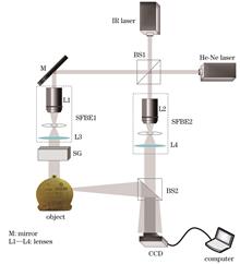
ObjectiveIn recent years, holography has developed rapidly, and has been applied to many scientific and technical fields. It has become a widely used experimental device and light source in three-dimensional (3D) imaging and display. After years of research and development, digital holography in visible wavelengths has become a crucial observation and detection method in the imaging field. However, the limitations of traditional visible light digital holography are becoming more and more obvious in the industrial area, where specific environments with smoke and flame interference exist. Scholars found that the ability of infrared (IR) light to pass through high-density particle fields is significantly higher than that of visible light, and infrared holography can be imaged through smoke and flames. This opens up new applications for holographic technology. However, in the smoke environment, the infrared digital holographic reconstruction image has serious scattering noise and prominent shadow areas, which can no longer meet the requirements for imaging quality. In this study, we propose an algorithm that applies to the reconstructed image of an infrared hologram in the presence of smoke motion. This algorithm can effectively suppress the scattering noise and achieve the effect of brightness enhancement. Thus, high-quality infrared hologram reconstructed images can be obtained using this algorithm.MethodsThe optical path of this study is designed and built based on the Mach-Zehnder interferometric optical path (Fig. 1). The optical path consists of laser, beam splitter, reflector, collimated beam expansion system, smoke generation device, and light sensor. The hologram acquisition time interval is set to keep the experimental setup stable and acquire 15 samples of infrared holograms under a relatively complete smoke change cycle. The algorithm in this paper is divided into four main steps: image pre-processing, segmentation of the target object, segmentation of the shadow region, and brightness enhancement of the shadow region. The specific algorithm flow is shown in Fig. 4. First, the image is pre-processed using a bilateral filter to remove significant scattering noise. Next, the image is binarized, the image edge information is extracted for expansion and filling operations, and the target object is segmented by combining the maximum connected area algorithm. An edge extraction algorithm and expansion and filling operations are then used to segment the shadow region from the target object area. Finally, an optimized sparrow search algorithm is used to enhance the shaded areas, and the brightness-enhanced reconstructed infrared holographic image is output.Results and DiscussionsIn this paper, six infrared holograms with significant continuous smoke changes were selected for reconstruction. The brightness enhancement algorithm of infrared digital holograms through smoke was used to enhance the brightness of the shadow region. Finally, the comparison results were obtained between the reconstructed and enhanced images (Fig. 10). We can judge and analyze the enhancement effect from Fig. 10 that the proposed algorithm eliminates the speckle noise of the image and retains the texture details. The shadow region’s brightness enhancement effect is obvious. Taking three infrared holographic reconstructed images [Figs. 10(a)-10(c)] as examples, four algorithms are compared (Fig. 11). The comparison shows that although the other three algorithms have their advantages, the final image quality cannot meet the experimental requirements. The proposed algorithm gives the best results. Next, the evaluation parameters including peak signal-to-noise ratio (PSNR), mean square error (MSE), and feature similarity index measure (FSIM) are calculated separately, and the results of the four algorithms are compared (Table 1). The PSNR value of the proposed algorithm is better than those of the other three algorithms, the MSE value is the lowest among the four algorithms, and the calculated FSIM value is also the closest to 1. The results show that the proposed algorithm achieves good luminance enhancement in the shadow region. It can achieve the brightness enhancement effect while suppressing the noise and maintaining the original structure of the reconstructed infrared hologram image with smoke motion.ConclusionsThe through-smoke infrared holographic reconstruction image has many problems, such as heavy scattering noise, uneven brightness and lack of object detail information. We propose a new image brightness enhancement algorithm, which can effectively improve the image quality of the through-smoke infrared holographic reconstructed image, with significant effects in brightness enhancement and removal of scattering noise. The experimental results show that, compared with other algorithms, the brightness enhancement algorithm of the through-smoke infrared digital holographic image has a better image enhancement effect, suppressing the scattering noise and showing evident brightness enhancement of the shadow region. In addition, from the analysis of image evaluation indexes, it is seen that the PSNR values of the proposed algorithm are all greater than 21, and they are higher than those of the comparison algorithms, indicating that the proposed algorithm has a better noise suppression effect. The MSE values are all less than 411, the smallest among the comparison algorithms, indicating that the image quality after processing by the proposed algorithm is the best. The FSIM values are all greater than 0.9511, the closest to 1. Compared with other algorithms, the results processed by the proposed algorithm have the highest similarity with the reconstructed images without smoke, exhibiting the complete structural recovery and the minor distortion. In summary, the algorithm proposed in this paper has a noticeable brightness enhancement effect in the shadow region, can intelligently process the acquired holograms, and can effectively improve the image quality of infrared holographic imaging in smoke permeable environment.
Sep. 25, 2023Vol. 50 Issue 18 1809001 (2023)
Xiangping Li, Guoxing Zheng, Xiaodi Tan, Shumin Xiao, and Lingling Huang
Sep. 25, 2023Vol. 50 Issue 18 1800101 (2023)
Linlin Su, and Chengdong Yang
ObjectiveSiC avalanche photodiodes (APDs) have the merits of visible light blindness, low weight, and high gain, exhibiting obvious advantages in weak ultraviolet detection. SiC APDs are mostly designed as pn junction structures, which can be divided into pin and nip APDs, according to the distribution of the epitaxial layers. When the SiC APD is conducting weak light detection, the device works under the avalanche state; the SiC pin and nip APDs exhibit completely opposite carrier drift directions. Holes in the pin APD drift toward the p-type layer, that is, the device surface, whereas the electrons drift toward the n-type layer, that is, the substrate; the nip APD exhibits the opposite. Cha et al. estimated the absorption coefficient of SiC at room temperature, and the results showed that SiC has a higher absorption coefficient for high-energy photons. Therefore, for the SiC pin and nip APDs, owing to the difference of the carrier drift direction, the types of carriers that cause collision ionization may be different for different wavelength detections . Considering that the collision ionization coefficient of holes in SiC is larger than that of electrons, different types of collision ionization carriers will certainly affect the detection performance of APDs. In this work, SiC nip APDs are designed and fabricated with a higher single photon detection efficiency for short wavelength ultraviolet light, benefitting from the hole dominated collision ionization process. This work is conducive for the in-depth understanding of the working mechanism of SiC APD and provides theoretical guidance for its optimization in the future.MethodsThe SiC nip APD is fabricated on an n-type 4H-SiC substrate (Fig. 1). The epitaxial structure is a 10 μm thick p-type contact layer (acceptor doping concentration NA=3×1018 cm-3), a 0.05 μm thick transition layer, a 0.7 μm thick n-type avalanche multiplication layer (donor doping concentration ND=1×1015 cm-3), a 0.2 μm thick n-type transition layer (ND=1×1018 cm-3), and a 0.15 μm thick n-type contact layer (ND=1×1019 cm-3) from bottom to top. The first step of APD fabrication is mesa etching. To suppress the peak electric field at the edge of mesa, the device is designed to be a beveled mesa structure (beveled angle of ~5°), and the etching depth is 0.5 μm. The epitaxial wafer is then passivated by the thermal oxidation layer and the plasma-enhanced chemical vapor deposition SiO2 layer. Finally, both the front and back contact metals (Ni/Ti/Al/Au) are deposited by electron-beam evaporation and annealed by rapid thermal annealing at 850 ℃ for 3 min in N2 ambience.Results and DiscussionsTo study the avalanche mechanism of SiC nip APD, the gain curves of SiC nip APD are plotted (Fig. 3). When the wavelength of the incident ultraviolet light increases from 220 nm to 320 nm, the breakdown voltage of the nip APD increases by 1.3 V. When the over bias is 3 V, the dark count rate is 1.7 Hz/μm2, and the single photon detection efficiency of the SiC nip APD for 240 nm and 280 nm incident UV light is 11.4% and 6.5%, respectively (Fig. 5). In the same working conditions, the single photon detection efficiency of the SiC nip APD for short wavelength ultraviolet light is evidently higher. The quantum efficiency of the SiC nip APD under 240 nm and 280 nm incident UV light is 15% and 45%, respectively (Fig. 6). Assuming that the SiC nip APD operates at 3 V overbias, the estimated photon avalanche probability is 84% and 16% at 240 nm and 280 nm illumination, respectively. It can be observed that the high single photon detection efficiency of the SiC nip APD for high-energy ultraviolet light is mainly related to the large photon avalanche probability. When the 240 nm ultraviolet light is incident on the SiC nip APD surface, photogenerated carriers are generated on the device surface and enter the depletion region through diffusion. Under the avalanche state, when the hole enters the depletion region, it drifts towards the substrate under the strong electric field, and its acceleration distance and collision ionization process span the entire depletion region. When the electrons drift towards the device surface after entering the depletion region, the acceleration distance and collision ionization process can be ignored. Thus, at 240 nm illumination, the avalanche process of the SiC nip APD is dominated by holes. With the increase of the ultraviolet light wavelength, the contribution of the electrons gradually increases. The collision ionization coefficient of holes in SiC is larger than that of electrons; therefore, the hole-dominated collision ionization process exhibits a higher avalanche gain and higher single photon detection efficiency.ConclusionsIn this work, SiC nip APDs are designed, and their avalanche characteristics are studied in detail. Under high energy ultraviolet light illumination, the avalanche multiplication process of the SiC nip APD is dominated by holes. With the increase of the incident light wavelength, the contribution of the electrons gradually increases. As the collision ionization coefficient of holes in SiC is larger than that of electrons, the SiC nip APD exhibits a higher gain and higher single photon detection efficiency for high-energy ultraviolet light illumination. The essential characteristics of the SiC nip APD ensure that the device is more suitable for short wavelength ultraviolet detection.
Sep. 25, 2023Vol. 50 Issue 18 1801001 (2023)
Yuanyuan Song, De Song, Ye Li, Weijun Chen, and Chunyang Liu
ObjectiveCurrently, in the information age, the realization of low light level digital night vision technology that can satisfy the remote transmission requirements of image information is urgently needed. The electron bombardment-type low light level imaging devices, namely, electron bombarded charge-coupled devices (EBCCDs) and electron bombarded complementary metal-oxide semiconductors (EBCMOSs), are used to package the back thinned charge-coupled devices (CCDs) and complementary metal-oxide semiconductor (CMOS) devices into an electric vacuum device. Accordingly, the chip replaces the microchannel plate and fluorescent screen to form a close proximity focusing system with the photocathode. Photoelectrons generated by the photocathode are accelerated by a high-voltage electric field and bombarded on the surface of the imaging device for direct imaging, which has many advantages, such as small size, high sensitivity, and ultra-low illumination. The processing steps in such imaging devices can be described as core making, back support, thinning, back processing, and tube sealing. Compared with EBCCDs, EBCMOSs, which are low light level imaging devices based on electron bombarded active pixel sensors (EBAPSs), have smaller size, faster imaging speed, low power consumption, and strong radiation resistance. Therefore, EBCMOS-based low light level night vision technology has become a popular research topic in the industry. Obtaining a high-gain EBCMOS electron multiplier layer is one of the key challenges in the development of EBCMOS low-light-level imaging devices. However, few relevant theoretical studies have been conducted to date. Therefore, this study focuses on the factors affecting the charge collection efficiency of electron multipliers in EBAPS imaging devices and builds a theoretical and technical foundation for constructing a high-gain EBCMOS electron multiplier.MethodsBased on the carrier transport theory and Monte Carlo simulation algorithm, a calculation model of the electron transport process in the passivation and electron multiplication layers of EBAPSs is established; moreover, the influence of structural parameters on the distribution and collection of secondary electrons is analyzed. First, the influences of SiO2 and Al2O3 passivation layers on the distribution and collection of secondary electrons are compared. Second, when the passivation layer material is SiO2, the influence of changing passivation layer thickness, incident electron energy, and P-type base thickness on the distribution and collection of secondary electrons is analyzed. Finally, the influence of changing doping concentration of the P-type base on the distribution and collection of secondary electrons is discussed. The simulation results provide a theoretical basis for device fabrication.Results and DiscussionsWhen the passivity layer material is SiO2, the charge collection efficiency is 42.5%, and the maximum incident depth and scattering radius of the incident electrons in the electron multiplication layer are 450 nm and 380 nm, respectively. With an increase in the incident depth, the distribution probability of the secondary electrons first increases and then decreases (Figs. 1 and 2). As the dead-layer thickness increases from 25 nm to 100 nm, the charge collection efficiency decreases. With an increase in the incident depth, the distribution probability of the secondary electrons first increases and then decreases. The probability trend of the secondary electron distribution with incident depth remains the same (Figs. 3 and 4). An increase in the incident photoelectron energy can improve the charge collection efficiency to some extent. With an increase in the incident depth, the probability of the secondary electron distribution first increases and then decreases. The greater the energy level, the greater the incident depth (Figs. 5 and 6). When the thickness of the P-type base increases from 5 μm to 20 μm, the charge collection efficiency decreases from 42.5% to 27.8% and collection efficiency of the center pixel decreases. In other words, the diffusion radius of the multiplier electron in the collection area increases, which is not conducive to constructing high-resolution imaging devices. With an increase in the incident depth, the distribution probability of the secondary electrons first increases and then decreases. The probability trend of the secondary electron distribution with depth remains the same (Figs. 7 and 8). The charge collection efficiency at different doping concentrations, ranging from 1015 cm-3 to 1019 cm-3, is simulated. It can be observed that the charge collection efficiency decreases as the doping concentration increases (Fig. 9).ConclusionsIn this study, the factors affecting the charge collection efficiency of the electron multiplier in EBAPS imaging devices are studied. When silicon dioxide with a low passivation layer density is used as the passivation layer, the incident depth of the incident photoelectrons improves; subsequently, the charge collection efficiency improves. Reducing the passivation layer thickness and increasing the energy of the incident electrons are beneficial for reducing the recombination of the secondary electrons in the dead layer, which improves the charge collection efficiency. Reducing the thickness and doping concentration of the P-type base is conducive to reducing the recombination of carriers while multiplying electron diffusion, thus improving the charge collection efficiency. The charge collection efficiency of the device after simulation optimization can reach 42.5%, which can provide theoretical support for the development of domestic EBCMOS devices.
Sep. 25, 2023Vol. 50 Issue 18 1803001 (2023)
Xing Zhou, Shumin Wang, Shucheng Xu, Jianqiu Ma, Lihua Lei, Zhishan Gao, and Qun Yuan
ObjectiveMorphological inspection is a significant step in the manufacturing process of precision machinery, integrated circuits, micro-optical devices, etc. Typical representatives are internal combustion engine fuel injectors, etched patterns on semiconductor silicon wafers, and micro-gratings. The presence of step-type structures on the surface of these components achieves certain special functions, which place nanometer-level requirements on the high measurement resolution of surface 3D morphology. Interferometric testing is a high-precision non-destructive measurement method for surface 3D morphology, which is combined with microscopic imaging technology to achieve microscopic morphology measurements. Depending on the magnification of the microscope, the lateral resolution varies from a few microns to hundreds of nanometers, and the field-of-view covers ~0.1 mm×0.1 mm to ~10 mm×10 mm. When the size of the part to be measured is large, the three-dimensional morphology measurement should be completed using stitching test. For some larger size parts to be measured, the lateral scale of the step-type structure is often larger, and the lateral resolution requirement of the measurement is reduced, which is no longer limited to the microscopic imaging method, and the reduced imaging scheme can be used to achieve direct measurement in a large field-of-view range. The goal of this study is to design and build a broadband optical interferometer with a large field-of-view to meet the inspection needs of large-size and step-type structure samples.MethodsFor the detection needs of special samples, this study selects a 1 inch detector and sets an imaging magnification target of 0.25×. According to this setting, we determine the field-of-view, numerical aperture, system focal length, and other system parameters of the entire system. After comprehensive consideration of the system's interferometric needs, this study uses the Köhler illumination system, double telecentric imaging structure, and sets a double flat tilted form of interference, which retains the characteristics of the Mirau-type structure with an equal light range and achieves a similar unobstructed effect as the Fizeau structure [Fig.1 (c)]. Subsequently, we select the appropriate initial structure using Zemax for the system design. After the system is built, the resolution plate and standard stage are selected for test verification and evaluation of the system.Results and DiscussionsThe large-field broadband optical interferometer designed and built in this study operates in the 480‒750 nm band and uses a 1 inch detector to form a measurement field-of-view of 47.60 mm×35.76 mm. This system consists of an illumination collimator, an interferometric cavity, and an imaging lens. The illumination collimator adopts the Köhler illumination, providing a uniform illumination object field-of-view with NA=0.015 and Φ=59.6 mm; the interferometer cavity retains the advantages of the Mirau-type equal-range interference and the Fizeau-type no-center-obstruction feature, and consists of a spectroscopic plate tilted at 1.5° and a reference plate tilted at 3° (Fig. 2); the imaging lens and collimator form a double telecentric imaging optical path with an imaging magnification of 0.25×, and the aberration correction reaches 0.24% in the wide spectral range (Fig. 8). The completed broadband optical interferometer was used to test the USAF1951 resolution plate with a system resolution of up to 14 lp/mm(Fig.12), and step plates with calibration heights of 7.805 μm and 46.554 μm were tested with the results of 7.833 μm and 46.552 μm, respectively. The height deviation for the step-type structure measurement was better than 0.4% (Figs.13‒14).ConclusionsTo address the problem that the existing interferometric inspection system is difficult to meet the efficient measurement of three-dimensional morphology of large-size step-type structures, this study begins with the basic optical path selection, then determines the optical structure form of double telecentric and Köhler illumination, and adopts a new interferometric cavity structure form that retains the advantages of the Mirau-type equal-range interference and the Fizeau-type no-center-obstruction feature. After designing the system using Zemax, the broadband optical interferometer system with a large field-of-view was obtained. The interferometer works in the wavelength range of 480‒750 nm and uses a 1 inch detector to achieve an imaging magnification of 0.25×, a measurement field-of-view of 47.60 mm×35.76 mm, and an aberration correction of 0.24% over a wide spectral range. The completed broadband optical interferometer was used to test the USAF1951 resolution plate, consisting of two step plates whose calibration heights were 7.805 μm and 46.554 μm. The test results show that the system’s measurement resolution can up to 14 lp/mm, and the height deviation of the step-type structure measurement is better than 0.4%. This broadband optical interferometer can achieve both larger field-of-view measurement and step-type structure measurements while retaining very high vertical resolution. It avoids the problem of low measurement efficiency caused by stitching when using the traditional interferometer to detect large-size step-type structure samples, which has a greater application prospect in the precision measurement of precision machinery, integrated circuits, and micro-optical devices.
Sep. 25, 2023Vol. 50 Issue 18 1804001 (2023)
Chanjuan Wu, Kaining Ying, Lunan Dai, Junfu Tan, Zhonghua Shen, and Chenyin Ni
ObjectiveWith the continuous emergence of various materials and the improvement of the quality requirements of modern industry for mechanical parts, non-destructive testing technology has been rapidly developed. Ultrasonic non-destructive testing has been widely used because of its high sensitivity, penetrability and other advantages; it has become an indispensable tool in aerospace, railway, oil pipeline, and other industrial testing. As a hot spot in the field of industrial non-destructive testing in recent years, phased array testing technology exhibits the characteristic of flexibility in focusing. However, all ultrasonic sub beams are focused at a constant depth, and reflectors outside the focus area cannot be detected sensitively. Synthetic aperture focusing technology (SAFT) can synthesize multiple small numerical aperture transducers into large numerical aperture transducers, which can obtain higher resolution reconstructed images and provide a more reliable basis for the qualitative analysis of defects. The total focusing method (TFM) is developed by combining phased array detection technology and synthetic aperture focusing technology. The total focusing method uses all the transceiver combinations in the phased array elements to detect defects and performs image post-processing on the obtained full matrix data. It uses all the information of the data to recover the detection signal to the maximum extent, and obtains imaging results with a stronger defect characterization ability and higher resolution. However, it has many limitations such as a large data demand, complex calculations, and the need for a substantial amount of time. To address these issues, the laser ultrasonic total focusing imaging method based on ZYNQ acceleration is studied in conjunction with laser ultrasonic testing technology.MethodsFirst, the total focusing imaging method based on laser ultrasound is established, and the laser ultrasound directivity coefficient is then introduced to optimize the algorithm by analyzing the imaging principle. Furthermore, a laser ultrasonic scanning detection device is built for experimental verification. The ultrasonic signal is excited by a linear laser source and the echo signal is detected by a Doppler vibrometer. The laser ultrasonic total focusing imaging method is then used to detect and locate the internal defects, and the results are compared with those obtained by synthetic aperture focusing technology. Finally, the personal computer (PC) is connected to the ZYNQ-7000 development board to test the data received by the PC. The total focusing imaging method is accelerated based on the loop expansion and pipeline principles of the ZYNQ programmable logic (PL) part and the dual core design principle of the processing system (PS) part, and the results are analyzed.Results and DiscussionsBefore and after the introduction of the laser ultrasonic directivity coefficient, the imaging results reflect the defect location (Fig. 10). In contrast, in the results obtained by the original total focusing method, the high amplitude signals are scattered around the defects. In the results obtained by introducing the laser ultrasonic directivity coefficient, the high amplitude signals are mainly concentrated at the defects, and the image signal-to-noise ratio is higher. Therefore, the introduction of the excitation directivity coefficient can effectively suppress noise and improve the image signal-to-noise ratio. Moreover, compared with the SAFT image (Fig. 11), the laser ultrasonic total focusing imaging method has a smaller defect position error, a higher signal-to-noise ratio of the defect image, and a stronger defect characterization ability. The algorithm is then transplanted to the ZYNQ platform for acceleration. Compared with the PC based imaging results, the imaging effects of the two are essentially the same (Fig. 12); however, ZYNQ has the advantages of time and cost (Table 2). The time consumption is reduced to 317/1000 that of the PC, and the cost is reduced to 3/10 that of the PC. This shows that ZYNQ has a higher cost performance ratio.ConclusionsAn algorithm of the laser ultrasonic total focusing imaging method based on ZYNQ is investigated in this study. The results indicate that the signal-to-noise ratio of the full focus image is improved significantly after the introduction of the laser ultrasonic directivity coefficient. Upon comparing the imaging results of synthetic aperture focusing technology and the total focusing imaging method, it is noted that the total focusing imaging method image has a smaller error and higher signal-to-noise ratio. The laser ultrasonic total focusing imaging method has a stronger defect characterization ability and higher signal-to-noise ratio, which further verifies the feasibility of the laser ultrasonic total focusing imaging method. After using ZYNQ to optimize the laser ultrasonic total focusing imaging method, it is deduced that the final imaging effect based on the ZYNQ calculation is essentially the same as that based on the PC calculation. However, the calculation time of ZYNQ is reduced by 86%, and the cost is reduced by 68.5%; this further confirms the feasibility of the laser ultrasonic total focusing imaging method based on ZYNQ.
Sep. 25, 2023Vol. 50 Issue 18 1804002 (2023)
Xingzhi Min, Yaxuan Duan, Zhengzhou Wang, Xiaoyi Chen, Zhiyuan Tang, Pu Wang, and Yao Fan
ObjectiveThe accuracy of a quadri-wave lateral shearing interferometer is directly affected by the accuracy of the wavefront reconstruction. Traditional wavefront-reconstruction methods include modal and zonal methods. The modal method expands the wavefront into a set of primary functions to be measured, then fits the coefficients corresponding to the primary functions to reconstruct the measured wavefront. The zonal method discretizes the measured wavefront to establish a mapping relationship between the measured and differential wavefronts for reconstruction. Alternatively, the wavefront can be reconstructed by direct integration in the shearing direction. However, the modal method always uses finite terms to fit the measured wavefront, which directly ignores high-frequency information, reducing the estimated accuracy of the quadri-wave lateral shearing interferometer. The zonal method has a high spatial resolution, but the noise error accumulates along the integrated path during the reconstruction process, forming noise lines, thus, affecting the accuracy of the reconstructed wavefront. To solve this problem, a quadri-wave lateral shearing interferometric wavefront reconstruction method is proposed based on path guidance, which has both high accuracy and spatial resolution.MethodsIn this study, a theoretical analysis of the drawbacks of noise error accumulation in wavefront reconstruction using the zonal method without integral-path guidance under noisy environments is carried out. An integral-path evaluation-map model is established based on the deviation of differential phase derivatives, and a flowchart of the wavefront reconstruction algorithm is provided based on integral-path guidance. The proposed method consists of two steps. First, the evaluation model of the differential-phase-derivative deviation is used to count the variational characteristics of the differential phase, identify the noise error, and generate an integral path to avoid noise error. Second, the generated path is used to guide the wavefront reconstruction integral of the Southwell model. Using theoretical simulations, the proposed method could effectively prevent the propagation and accumulation of noise errors compared to the zonal method without integral-path guidance under noisy environments for different signal-to-noise ratios (SNRs). In addition, a verification device having a pure-phase liquid-crystal spatial light modulator (SLM) was set up to experimentally verify the effectiveness of the proposed method. The experimental results of the proposed method were also compared with those of the zonal method without integral-path guidance.Results and DiscussionsIn the simulation, interferograms with a sinusoidal phase distribution are generated (Fig. 4). When the SNR increases from 10 dB to 50 dB, the root-mean-square (RMS) between the wavefront reconstructed by the zonal method without integral-path guidance and the theoretical wavefront decreases from 0.0152λ to 0.0094λ. However, the RMS between the wavefront reconstructed by the proposed method and the theoretical wavefront decreases from 0.0139λ to 0.0041λ. Moreover, the proposed method reduces the RMS of the reconstructed and theoretical wavefronts by a maximum of 55.6% compared to the zonal method without integral-path guidance (Fig. 7). Thus, the proposed method is more robust than the zonal method without integral-path guidance under the Gaussian noise environment with different SNRs (Fig. 6). In the experiment, we measure the random phase generated by the spatial light modulator using the proposed method and zonal method without integral-path guidance (Fig. 10). The results show that the PV value (peak-valley value) of the wavefront reconstructed by the proposed method is 0.7283λ, whereas that of the wavefront reconstructed by the zonal method without integral-path guidance is 2.966λ. The deviation between the PV value of the wavefront reconstructed by the proposed method and that of the theoretical wavefront is 1.6943λ, which is less than the deviation between the wavefront PV value reconstructed by the zonal method without integral-path guidance and the theoretical wavefront PV value (Fig. 13). In addition, the RMS between the wavefront reconstructed by the proposed method and the theoretical wavefront is reduced by 39.7% compared with the RMS between the wavefront reconstructed by the zonal method without integral-path guidance and the theoretical wavefront. In addition, the zonal method without integral-path guidance is used to reconstruct the wavefront, which propagates and accumulates noise points along the shearing direction by forming noise lines. However, the proposed method prevents the propagation of noise points and improves wavefront reconstruction accuracy.ConclusionsThis paper proposes a quadri-wave lateral shearing interference wavefront reconstruction method based on integral-path guidance. The effectiveness of the proposed method is verified through theoretical simulations and experiments. The theoretical simulation results show that the proposed method prevents the propagation of noise errors and improves the wavefront reconstruction accuracy compared to the zonal method without integral-path guidance under noisy environments with different SNRs. The RMS between the reconstructed wavefronts of the proposed method and the theoretical wavefront is smaller than that between the zonal method without integral-path guidance and the theoretical wavefront under the same conditions. Moreover, the experimental results show that the proposed method can effectively prevent the propagation and accumulation of differential phase noise points when measuring the random phase generated by the pure-phase liquid crystal spatial light modulator and reconstructing the wavefront of the random phase. However, the wavefront of the random phase reconstructed using the zonal method without integral-path guidance cannot be accurately reconstructed because of the noise line generated by the accumulation of noise. Therefore, the proposed method has higher accuracy and robustness than the zonal method without integral-path guidance in reconstructing the wavefront in a noisy environment.
Sep. 25, 2023Vol. 50 Issue 18 1804003 (2023)
Renfang Geng, Zhibo Wu, Yong Huang, Haisheng Lin, Rongzong Yu, Kai Tang, Haifeng Zhang, and Zhongping Zhang
ObjectiveSatellite Laser Ranging (SLR) has contributed a new prospect to clock comparison and monitoring with higher precision and accuracy. Several laser time transfer projects, such as Time Transfer by Laser Link (T2L2), and Laser Time Transfer in China’s Space Station (CLT), have been conducted over the past 20 years. However, the traditional laser time transfer is limited because of incident light intensity and ambient temperature on onboard hardware. Alternatively, Forward Laser Time Transfer (FLTT) based on curved mirrors is a new type of laser time transfer technology with great application potential, which has the advantages of zero-time delay in the forward process, high reliability, long service life, and high measurement accuracy. However, due to the lack of suitable satellite experimental platforms, experimental data and performance evaluation results of the FLTT have not been obtained. The current research is only limited to theoretical analysis. In this study, we investigated the FLTT with two adjacent SLR systems as the test station and the retroreflectors on the cooperative target satellite as the forward payload. Our research should provide some technical reserves for the curved mirror based FLTT and evaluate the feasibility and performance of FLTT technology.MethodsFirst, we briefly introduced the basic principles and difficulties of FLTT, including one-way and two-way FLTT modes. Furthermore, the clock difference extraction algorithm of a one-way FLTT was improved to make it suitable for laser time transfer scenarios with high precision and accuracy. Then, two sets of FLTT test systems were built through the adaptive transformation of the SLR systems of the Shanghai Astronomical Observatory (SHAO). Among them, we added the precise control circuit of the laser emission epoch, the calibration device of the FLTT system time delay, and the clock difference extraction module. Depending on the two FLTT systems, we carried out one-way and two-way FLTT experiments, homologous clock FLTT experiments for BDS45 and BDS22 satellites, and non-homologous clock FLTT experiments for BDS21 and Galileo206 satellites. In addition, we obtained the real clock difference of the two FLTT systems with a DG645 delay signal generator, which is the clock difference obtained by the electrical signals, and then the reliability of the clock difference of one-way and two-way FLTT experiments was demonstrated. Finally, we analyzed the FLTT results and studied the main factors that affect the performance of this technology.Results and DiscussionsBased on BDS45, BDS22, and other satellites, the FLTT experiments in one-way and two-way modes were carried out, and both obtained a precision better than 100 ps (Fig. 8, Fig. 9, Fig. 10, Fig. 11). There are two critical issues to realize FLTT using curved mirrors. One is the limited hitting probability at the right time and another issue is the weak strength of reflected signals. Therefore, the one-way FLTT mode will have better applicability in the future. The results of the one-way FLTT were similar to those of the two-way FLTT (Fig. 10 vs Fig. 11, Fig. 11 vs Fig. 12), which verified the reliability of the improved clock difference extraction algorithm in this study. Compared the FLTT experiment results and the clock difference obtained by the DG645 electrical signals, the absolute accuracy was better than 2 ns, demonstrating the reliability of the FLTT experiments (Fig. 12). However, there was plenty of room for improvement. In the FLTT with the homologous clock, the clock difference jump phenomenon was caused by the synchronization of the event timer and clock. In the FLTT with non-homologous clocks, the clock difference fluctuated greatly due to the poor stability of the End-run clock.ConclusionsThe curved mirror-based FLTT has been considered a more accurate and stable time transfer technique than existing methods, which is a popular scheme for the next generation of laser time transfer. However, there is a lack of suitable test platforms for validation purposes, and the current research interests in FLTT remain in theoretical simulation. In this study, we selected satellite reflectors instead of curved mirrors as a forwarding payload for the FLTT experiments, demonstrating the feasibility and performance of this technique. We improved the clock difference extraction algorithm of the one-way FLTT and proposed a high-precision interpolation model. It was shown from the results that the precision was better than 100 ps with an absolute accuracy of 2 ns, and the one-way FLTT was feasible. Of course, the FLTT will probably face other challenges in practical application, such as weak laser echo signal recognition, and the probability of success is affected by the attitude and rotation period of satellites. This study provides significant support for FLTT development, such as in laser emission timing control, data processing, and more.
Sep. 25, 2023Vol. 50 Issue 18 1804004 (2023)
Dahuai Zheng, Shuolin Wang, Junkun Chen, Yuqi Zhang, Hongde Liu, Mengxin Ren, Yongfa Kong, and Jingjun Xu
SignificanceLithium niobate (LN) crystal is a kind of multi-function and multi-purpose artificial crystal material, which has the advantages of good temperature stability, easy optical cold processing, and properties control. As a typical photorefractive (PR) crystal, LN is widely used in research and applications in high-density optical storage, laser physics, information processing, computing, etc. With the rapid development of information science and technology, magnetic tape, disk, and optical disc cannot meet the increasing demand for data storage. The theoretical limit of holographic three-dimensional (3D) storage capacity can reach 1012 bit/cm3, which is much higher than the traditional one-dimensional (1D) and two-dimensional (2D) memory. Meanwhile, real immersion experience makes 3D display a huge market demand. The dreamed 3D display in the future should be viewed without auxiliary wearing devices. Holographic display is one of the techniques to realize 3D display. Then, with the enormous demand and rapid development of massive storage and dynamic holographic display, 3D optical storage and dynamic display based on LN crystals have once again become a research hotspot.ProgressHere, we present an overview of the principles, history, and recent advances in holographic data storage and display based on LN crystal. Compared with the commonly used liquid crystal display materials, LN crystals present many advantages, such as good temperature and chemical stability, high diffraction efficiency, and no need to apply high voltage. The photorefractive response of LN crystal is significantly improved by the doping of cations containing lone-pair electron, and the response time of bismuth and magnesium co-doped LN crystal is reduced to 7.2 ms under the activation of 442 nm laser, which meets the requirements of real-time dynamic holographic display. The crystal has been used to demonstrate a real-time holographic display with a refresh rate of 60 Hz, as that of the high-definition television. It seems that LN∶Bi,Mg is a suitable candidate material for holographic 3D display. Meanwhile, a reasonable calculation is carried out to understand the mechanism of its fast response. The results indicate that the electron mobility while Bi occupying Nb-site is significantly greater than that in Li-site, which directly induces the fast response of LN∶Bi,Mg crystals when the concentration of Mg is beyond its doping threshold. This work provides an ideal candidate material for holographic 3D display and expands the technique for performance control of LN crystals. In addition, doping high valence ions (vanadium and molybdenum) can significantly affect the photorefractive performance of LN crystals. Molybdenum and magnesium co-doped LN crystal can exhibit excellent photorefractive performance in all visible light bands, bringing hopes for real-time refreshable color holographic displays.Conclusion and ProspectsDue to its excellent photorefractive properties, LN has become a major candidate material for holographic 3D storage and display. With the rapid development of Internet technology, such as cloud computing, high-density and large-capacity optical holographic 3D storage based on LN crystals provides a solution to the increasingly urgent demand for massive data throughput. However, the improvement of information loading and extraction speed and the extension of fixed and storage life still need further study. With the rise of virtual reality (VR), augmented reality (AR), meta-universe, and other concepts, 3D display has shown great application prospects and economic benefits. Photorefractive holographic display that can be written and read in real time is an important technology for realizing 3D dynamic display. Therefore, it is necessary to continue to carry out in-depth research on the improvement of the response of LN crystal in red, green, and blue bands and to arrange dynamic holographic display devices and technology research in advance.In addition, thanks to the sub-micron LN single crystal thin film preparation as well as the industrialization of mature semiconductor micro-nano processing technology in preparation of LN micro-nano devices, just after a few years, the research on the new effect of LN on insulator (LNOI) and micro-nano optics has made remarkable achievements. High-performance electro-optical modulators, lasers, amplifiers, waveguides, and other functional devices and transmission devices on the LN chips have been successfully fabricated, and LNOI has become one of the new generations of excellent integrated photonics platforms. With the in-depth research of LNOI-based integrated optics and new effects, photorefractive effect is also shown in the research of on-chip micro and nanodevices. Like bulk LN crystals, photorefractive effect is also a double-edged sword for applying micro and nanodevices of submicron LN films. On the one hand, photorefractive effect can adversely affect the performance of frequency comb and microwave photonics devices, but some micro and nanodevices, on the other hand, also show fast photorefractive response, which provides an opportunity for the research of editable photonics devices. Therefore, the photorefractive effects and applications of LNOI-based micro-nano systems and related integrated optical systems are also worthy of attention.
Sep. 25, 2023Vol. 50 Issue 18 1813001 (2023)
Jiajia Wu, Kai Gao, Chenduan Chen, Zhiqiang Wang, Jianrong Qiu, and Dezhi Tan
SignificanceInformation storage is an important means of human civilization inheritance and a necessary link for social and economic development. With the advent of the era of big data, the amount of data generated by various industries is increasing explosively, presenting mankind with an unprecedented flood of data. According to International Data Corporation (IDC), the global data volume will reach 175 ZB by 2025. Therefore, achieving low energy consumption and long-term secure data storage is an urgent task for the construction of digital society. At present, widely used data storage devices, such as magnetic tapes, hard disks, and solid-state drives, generally face the problems of high energy consumption and short life. In contrast, although optical storage has slow read-write speed and small capacity, it has unique advantages in terms of cost, energy consumption, reliability, and service life, and is considered likely to be one of the most important directions of development in the field of information storage in the future. As an ideal optical storage medium, glass has excellent thermal, optical, and chemical stability, and its data storage life can even reach hundreds of millions of years. Therefore, new optical storage technology using glass as the storage medium provides an effective solution for the permanent storage of large-scale warm and cold data, which is of great significance for alleviating the pressure of big data storage and ensuring the safe and efficient development of China’s digital economy.In recent decades, researchers have continuously explored the relevant mechanisms and technical means for optical storage in glass, making significant progress. However, from the perspective of practical application and industrialization, glass optical storage still faces certain challenges. Therefore, a summary and prospect of current research are of important reference value for the future development of this field, which is also necessary.ProgressWe review the research progress and dimension multiplexing of glass optical storage in recent years. First, we introduce femtosecond laser-induced multi-dimensional optical storage technologies based on refractive index change, anisotropic periodic nanostructure formation, ion valence change, metal nanocluster/particle formation, and quantum dot/nanocrystal precipitation, including their formation mechanism and performance parameters, such as storage density and storage life. We then discuss some challenges in the field and analyze the potential of light field modulation technology and deep learning technology to improve the performance of optical storage.Conclusions and ProspectsGlass optical storage technology provides an effective solution for the permanent storage of information in the big data era. In summary, current glass optical storage technology is developing toward ultra-high density, multi-dimensional multiplexing, ultra-fast reading and writing, erasable rewriting, and ultra-long life. Its practicality and industrialization merit further exploration. We firmly believe that in the near future, the realization of glass optical storage technology with large storage capacity, ultra-fast reading and writing speed, and ultra-high reading and writing precision will open new opportunities for the innovation of data storage systems.
Sep. 25, 2023Vol. 50 Issue 18 1813002 (2023)
Dejiao Hu, Zhen Wang, Tiewei Luo, Qifan Xia, Diqin Zhang, Yuxia Zhao, Mu Zheng, Xiangping Li, and Yaoyu Cao
SignificanceWith the explosive growth of global data in the information age, the amount of data to be stored is increasing exponentially. The secure, stable, and long-term storage of vast amount of data generated by the internet in various scenarios has become the foundation for the sustainable development of future information technology. The capacity of a single hard disk drive (HDD) can be as large as 20 TB, which plays an important role in many applications. An HDD is a typical magnetic data storage technique. However, the rapidly developing technology of solid-state disks (SSD), which employ electronic circuits to store and retrieve data, is superior in terms of a high transfer rate and favors applications requiring frequent data exchange. However, both magnetic- and electronic-circuit-based data storage have the disadvantages of high energy consumption, short lifetime, low safety, and poor stability. These issues become increasingly obvious for the storage requirement of “cold data,” which have large size and needs to be accessed less frequently. Optical data storage (ODS) has the advantages of low energy consumption, long lifetime (as long as 50 years), high safety, and high stability. Consequently, the utilization of the ODS technology in the field of large data storage has attracted considerable attention.The conventional ODS technique employs a focused laser spot to record and read data, and the data density depends on the lateral size of the laser spot. Based on this concept, the ODS industry developed compact discs (CD), digital video discs (DVD), blue-ray discs (BD), and archival discs (AD). In 2019, Sony released a second-generation AD with a capacity of 500 GB per disc. The minimum size of the data bit on the disc was approximately 68 nm, which is close to the physical limit of this technique. Further increase in the capacity requires an increase in the number of recording layers, which causes serious interlayer interference and limits the maximum number of layers. Inorganic glass was used as the recording medium to further increase the archive lifetime. Microsoft reported their silica-based compact discs in 2019, where data was recorded inside silica disc in the format of multi-layered 3-dimensional (3D) data bit called “voxel.” This technique is based on the interaction between a focused femtosecond laser and quartz that generates micro-gratings for data encoding. However, it exhibits drawbacks, such as a relatively low transfer rate, large physical size, and high cost.Holographic data storage (HDS) records data in photosensitive media in the form of holograms by utilizing the coherence of the laser beam, where the recorded data are represented by the amplitude, phase, or polarization of the light wave. In a parallel storage scheme, the data are scribed into 3D volume space, which makes full use of the thickness of the media and increases the storage capacity. The data is recorded and read as a 2-dimensional (2D) coded data page, which enables a high transfer rate of up to several hundred million bits per second (GBPS). Its predominant performance potential makes HDS the best candidate for next-generation optical data storage technology.ProgressThe foundation of the HDS technology lies in its multiplexing recording method, which guarantees a large storage capacity. HDS techniques can be categorized into two classes according to the relationship between the reference and signal beams: coaxial and off-axis. Coaxial HDS has an axially symmetric record and read beam, where the reference and signal beams share the same optical axis. Whereas, in an off-axis HDS system, the reference and signal beams are directed onto the media at a nonzero angle of incidence. Multiplexing techniques, such as orthogonal coding, phase-coding, and shift, can be employed in coaxial HDS systems. Commonly used multiplexing techniques for off-axis HDS systems include angular, peristrophic, and spherical reference wave-shift multiplexing. The HDS encompasses the practical implementation of various techniques, including optical, servo, signal processing, and coding systems. In 2000, Stanford University demonstrated a coaxial HDS prototype with a transfer rate of 1 GBPS using a pulsed laser as the light source. Subsequently, Sony designed an image-stabilizing technique for a coaxial holographic disk system to increase the transfer rate using a low-peak-power continuous laser. Around 2006, Optware and Sony demonstrated their prototype with a capacity of about 200 GB to 1 TB. During the same period, InPhase released its HDS drive, Tapestry, which employed an angular multiplexing method to increase data density. It has a capacity of 300 GB and a transfer rate of 20 MBPS. After 2017, Tokyo University of Science and Amethystum Storage Technology Co,. Ltd. developed an HDS system based on spherical reference wave cross-shift multiplexing, which combines shift and peristrophic multiplexing techniques. The shift interval can be as small as 5 μm, which enables a high multiplexing density (Fig. 3). Furthermore, the prototype was provided with a single-arm architecture, in which the reference and signal beams pass through the same relay lens system and split into two beams immediately before the recording media. This design reduces the path along which the reference and signal beams are separated, leading to a compact size and stable performance (Fig. 4).Another core foundation for HDS is the recording media. Photopolymer materials are regarded as the best candidates to date. Dynamic range, photosensitivity, shrinkage rate, scattering, and lifetime are used to characterize the performance of the media. The dynamic range is the largest amplitude of refractive index modulation that the media can achieve, restricting the maximum multiplexing density from the media aspect. A larger dynamic range allows for a higher multiplexing density and capacity. However, a large dynamic range is always accompanied by a large shrinkage rate, which is induced by the polymerization of monomers and can result in the complete deterioration of the hologram. To guarantee a high signal-to-noise ratio (SNR) for the readout data page, the shrinkage rate is typically required to be less than 0.1%. Photosensitivity is the main factor influencing the recording rate. Larger photosensitivity reduces the requirement of high laser power and complexity of the mechanism; however, it may decrease the lifetime owing to high chemical activity. Materials with superior comprehensive performance have been developed by Aprilis, InPhase, Akonia Holographics, and Mitsubishi Chemical (Table 1).Conclusions and ProspectsHDS is a prominent candidate for next-generation optical data storage owing to its high storage density and potentially high transfer rate. The main obstacle for HDS to enter practical applications is the recording medium. Intensive studies on photochemical kinetics, particularly on the interaction between two multiplexed holograms during the recording process, are required. In addition to its applications in the field of big data, HDS has great potential in the field of artificial intelligence. Specifically, it offers promising prospects for storing the weight matrices of neural networks in holographic media, thereby enabling fast parallel calculations.
Sep. 25, 2023Vol. 50 Issue 18 1813003 (2023)
Rui Wei, and Yanjun Bao
SignificanceOptical encryption is a technique that uses light as a multidimensional carrier of information to encode and decode plaintext images through optical transformations. It has advantages over traditional encryption methods in terms of complexity, security, robustness, and reliability. However, conventional optical encryption schemes often rely on complex and bulky optical components that limit their efficiency and portability. Metasurfaces are artificial structures that can manipulate light at subwavelength scales and control its amplitude, phase, and polarization. They provide a flexible and efficient platform for optical encryption by using different metasurface structures to modulate the incident light and generate encrypted images. The basic principle of metasurface optical encryption is to use the structure to control the input and output keys of the light, the optical parameters modulating the incident light and encrypted image respectively. Only by knowing the correct input and output keys can one decrypt the image and recover the original information. The metasurface structures can utilize different dimensions of light at the input and output ports, such as wavelength, polarization, incident angle, and distance, to achieve single- or dual-port encryption. This study summarizes and discusses three types of metasurface optical encryption schemes, namely, single-input port, single-output port, and input-output port combination, as shown in Fig. 1.ProgressMetasurface-based optical encryption can utilize the multiple dimensions of light at the input and output ports. For any light beam, all of its parameter dimensions at the input and output ports have definite values, and identifying the dimensions that are used for encryption when information for only one image exists is difficult. Therefore, we focus on the optical encryption that changes at least one or more dimensions to encrypt multiple image signals. The optical encryption based on a single-input port is first discussed, where the analyzed parameters at the output port are fixed. For optical encryption at an input port, we discuss the use of only one parameter dimension, such as wavelength, polarization, and incident angles, to encrypt image signals (Fig. 2). The multiple optical parameter dimensions at the input port can be combined to encrypt different image signals to provide more independent encryption information channels (Fig. 3). At the output port, the dimensions of light can be used for optical encryption, whereas those at the input port are fixed (Fig. 4). Finally, input-output port joint optical encryption schemes are discussed, where different combinations of optical parameter dimensions at the input and output ports are used to encrypt and decrypt the image signals. These include polarization dimension input-polarization dimension output (Fig. 5), polarization dimension input-multiple dimension output (Fig. 6), wavelength dimension input-other dimension output (Fig. 7), incidence angle dimension input-diffraction distance dimension output (Fig. 8), and multiple dimension input-other dimension output (Fig. 9).Conclusions and ProspectsWe discuss the recent progress and challenges of metasurface optical encryption. Various optical-field manipulation mechanisms have been previously proposed based on metasurfaces, which can achieve different degrees of freedom of the Jones matrix from one to eight, the highest possible in nature. This multiple-degree-of-freedom optical-field manipulation and new mechanisms lay the foundation for enhancing the complexity and security of optical information encryption. However, challenges remain in the field of metasurface optical encryption, such as the crosstalk phenomenon, limited utilization of light dimensions, lack of integration with other physical signals, and absence of dynamic control capabilities. We suggest that further research can be conducted to optimize and improve the performance and reliability of metasurface optical encryption and storage.
Sep. 25, 2023Vol. 50 Issue 18 1813004 (2023)
Ziting Liu, Yiming Yuan, Ziyue Li, Wei Gong, Xu Zhang, Xinjing Zhao, Yi Wang, Zhenze Li, and Lei Wang
SignificanceSince the beginning of the 21st century, with the rise of the internet, artificial intelligence, cloud computing, and cloud storage, the amount of data generated has grown exponentially, thus leading to a sharp increase in the demand for data storage. According to the International Data Corporation (IDC), by 2025, the world is expected to produce a total of 175 ZB (1 ZB=1012 GB) of data, of which approximately 10%‒15% is expected to eventually evolve into cold data, which does not require frequent access but needs to be stored for a long time. Such data include the National Archives Center data, human civilization events, and scientific achievements.Cold data can be stored in several ways, including in mechanical hard drives, solid-state drives, and tape storage. Among these, magnetic storage has problems, such as vulnerability to damage and high environmental requirements. In comparison, optical storage technology is durable, lighter, more energy-efficient, and has lower environmental requirements. Optical disk storage uses lasers to modify and engrave 0 and 1 on the surface of photosensitive materials to achieve storage. However, further reducing the point size of optical storage is challenging owing to the diffraction limit; consequently, increasing the capacity of optical disks is challenging.A possible solution for increasing the storage capacity and reducing the refresh rate involves shifting from 2D storage to 3D storage, and from organic storage to inorganic optical storage. Femtosecond laser optical storage, which uses ultrafast lasers with extremely high peak powers to store data inside hard materials such as glass, sapphire, and diamond, has become a potential solution. Since 2003, several research institutions, including Kyoto University in Japan; the University of Southampton in the UK; and Tsinghua University, Huazhong University of Science and Technology, and Jilin University in China have introduced five-dimensional optical storage technology. Hitachi and Microsoft Research in Cambridge have also introduced unique ultrafast laser optical storage solutions.However, femtosecond laser-based optical storage cannot meet industrial demands in terms of writing speed and storage capacity because of the complexity of the ultrafast action mechanism. Different powers, pulse numbers, and pulse widths produce different types of phase changes, thus affecting the optical properties of storage units and resulting in complex refractive index changes in the spatial distributions and birefringence properties. This correspondingly requires dozens or even hundreds of pulses, with pulse energies of tens to hundreds of nanojoules. Additionally, it prohibits both further reduction in the point spacing and interlayer spacing for high-density storage, and efficient processing through beam splitting with limited ultrafast laser energy, thus increasing the difficulty of industrialization. A study on the formation mechanism can offer ideas for accelerating the introduction of nanograting. Therefore, the formation mechanisms of the laser-induced modifications must be summarized.ProgressHerein, we reviewed nearly 20 years of ultrafast mechanisms of interaction between lasers and transparent hard materials. First, we analyzed the physical process of the interaction between the femtosecond laser and transparent hard materials on a timescale. To specify the interaction between the femtosecond laser and transparent materials, the modification process and influencing factors induced by the femtosecond laser were investigated in detail. Based on the different types of structures induced by the femtosecond laser, the structures were divided into positive refractive index changes (Type Ⅰ), negative refractive index changes (Type Ⅱ), and scattering-based modification types (Types Ⅲ and Ⅳ). The formation mechanism and applications of each modified structure were discussed, and the application of nanogratings to 5D optical storage, including the principles, progress, and prospects, was explained in detail.However, some problems remain in optical data storage based on nanogratings, such as low storage capacity and slow data-writing speed, must be overcome. To compensate for the deficiencies of this technology, new types of structures, namely Types X and S, were proposed herein. Type X nanopores are randomly distributed and generated by laser pulse width modulation, and are transient states between Types I and Ⅱ. These structures have very high transmittance, which is key for improving the storage capacity. Type S is an anisotropic nanolamella-like structure produced by fast pulse energy modulation, which can minimize unnecessary thermal effects caused by femtosecond pulses. These structures can improve the data writing speed.Finally, we presented the challenges of 5D eternal optical storage as well as feasible solutions. Combined with the theory of far-field-induced near-field breakdown, the development of new materials is a promising research direction.Conclusions and ProspectsEternal optical storage is a feasible solution for the demands of the big data era. However, the capacity and the writing speed both limit the practical use of this technology. Many researchers are attempting to overcome these problems and have made progress. We believe that external optical storage will be practical in the future.
Sep. 25, 2023Vol. 50 Issue 18 1813005 (2023)
Chen Zhu, Zhenglong Shao, Yingjie Zhou, Jiaqi Ren, Fan Fan, and Dongliang Tang
SignificanceAs a class of soft functional materials that exhibit both liquid and solid-like properties, liquid crystals can simultaneously show fluidity and crystal anisotropy, and have been widely applied in the fields of image display, integrated optoelectronics, optical communication, and others. In the past decades, with the development of the liquid crystal theory and processing technology, the research on liquid crystals has gradually matured from the conventional display to advanced liquid crystal photonics, which is of great significance for the realization of integrated, intelligent, and miniaturized optical systems. Liquid crystals can exhibit abundant phase states, including smectic, nematic, cholesteric, and blue phases. Each phase state has its unique properties and can be applied in different fields, including tunable optical devices and polarization converters. Therefore, the light modulation characteristics of liquid crystals, including their amplitude, phase, and polarization, are investigated. Based on these properties, a variety of liquid crystal devices can be designed to replace the conventional refraction optical elements, such as gratings, focusing lenses, spiral phase plates, beam steering devices, and holographic imaging devices. For the successful fabrication of devices, liquid crystal molecules should be controlled precisely in terms of the friction orientation, tilt evaporation orientation, and photoalignment. Each technology has its unique advantages from the perspective of different applications. In addition, liquid crystals can be dynamically controlled by varying the electric field, magnetic field, or temperature. The use of liquid crystals in the field of lasers and metasurfaces is of great significance to prepare tunable liquid crystal micro-laser and liquid crystal metasurface composite devices. Therefore, it is extremely important and necessary to summarize the liquid crystal modulation techniques to guide the future development of this field.ProgressThis paper summarizes the research progress in multi-dimensional light modulation enabled by liquid crystals. The light modulation characteristics of liquid crystals are derived from their birefringence properties through the Jones matrix (Fig. 2). A variety of photoalignment technologies, including mask exposure, interference exposure, direct write exposure, plasma mask exposure, and dynamic mask exposure, are presented (Fig. 3). According to the light modulation characteristics of liquid crystals, liquid crystal devices are classified into amplitude, phase, and complex amplitude types. Amplitude-type liquid crystal devices include liquid crystal displays, amplitude-type spatial light modulators, and liquid crystal smart windows (Figs. 5-7). Phase-type liquid crystal devices include phase-type spatial light modulators and geometric phase-type liquid crystal devices. The researchers developed an orbital angular momentum holographic encryption system based on a phase-type spatial light modulator. For geometric-phase liquid crystal devices, some geometric-phase nematic liquid crystal devices are first introduced. In order to overcome the low polarization conversion efficiency of nematic liquid crystals, the researchers from Nanjing University obtained a chiral flip controllable self-assembled spiral superstructure by mixing a photosensitive molecular machine with a chiral agent with opposite chirality. An optically controlled transformable optical device with a continuously adjustable working band and geometrically conjugate phase was realized (Fig. 10). By introducing the extension of Marius' law to the orientation arrangement of liquid crystal molecules, the researchers from Wuhan University realized the independent regulation of the amplitude and phase of light waves, realizing a breakthrough in ultra-compact multifunctional liquid crystal devices (Fig. 12). Based on the Jones matrix, the researchers from Hunan University found that binary phase modulation also contributes to continuous amplitude modulation and realized a complex amplitude liquid crystal device (Figs. 13 and 14). The concept of metasurface has attracted considerable attention in recent years. However, once the structure of the metasurface is determined, it is difficult to realize dynamic modulation. To overcome this situation, researchers have combined metasurfaces with liquid crystals to achieve dynamic control of the optical properties of the integrated system (Figs. 15 and 16). Benefiting from the liquid, self-assembling, and tunable properties of liquid crystals, researchers have developed liquid crystal-based micro-lasers (Fig. 17). In addition, other light modulation applications enabled by liquid crystals, including nonlinear optical effects and optical angular momentum modulation, have been discovered (Figs. 18 and 19).Conclusions and ProspectsWith the development of the liquid crystal research theory and fabrication/processing technologies, different light-modulation technologies based on liquid crystals have been developed for various optical applications ranging from conventional display amplitude modulation to geometric phase modulation, and complex amplitude modulation, static to dynamic modulation, and single-function to multi-function integration. This paper outlines the recent research progress of multi-dimensional light modulation based on liquid crystals, especially the design and processing of multifunctional liquid crystal devices. At the same time, combining a dynamically controllable liquid crystal with a metasurface to form a composite structure can integrate more functions in a single device. The field of liquid crystals also faces certain issues in aspects ranging from structural design to device fabrication, such as how to achieve multifunctional multilayer integrated liquid crystal devices, broadband achromatic liquid crystal devices, polarization-independent liquid crystal devices, vertical chromatic aberration correction of liquid crystal devices, and zoom liquid crystal lenses. Therefore, it is necessary to focus on the above areas, and we believe that optical devices based on liquid crystals will play an increasingly important role in optical encryption, image display, optical communication, and data storage.
Sep. 25, 2023Vol. 50 Issue 18 1813006 (2023)
Sihua Su, Kaiyang Wang, Can Huang, Limin Jin, Shumin Xiao, and Qifeng Ruan
SignificanceStructural color arises from the interaction between light and structures. Compared with the colors produced by traditional dyes, structural colors are usually environmentally friendly and resistant to fading. The two-photon polymerization-based three-dimensional (3D) printing technology provides sufficient freedom for the structural design and control of the full three-dimensional space and possesses higher resolution than traditional 3D printing technologies. Therefore, it has been widely used in the preparation of high-resolution structural colors in recent years. This review first briefly describes the principle and characteristics of two-photon polymerization 3D printing technology. We then introduce representative structural color schemes such as 3D printed diffraction gratings, photonic crystals, biomimetic structures, and single nanopillars. We also review 3D and dynamic structural colors for optical anti-counterfeiting, information storage, and optical sensing. Finally, the research status, existing problems, and future research directions of two-photon polymerization 3D printing technology are discussed.ProgressThe emergence of two-photon polymerization lithography (TPL) has successfully improved 3D printing resolution to submicron and nanometer levels. In 1997, Maruo et al. used TPL to fabricate micron-scale helical 3D polymer structures for the first time, and the field of two-photon processing was launched. In 2001, Kawata et al. used a near-infrared femtosecond pulsed laser to induce two-photon polymerization of photoresist to manufacture “micro-bull” sculptures. Its spatial resolution reaches 120 nm, which can be regarded as a milestone of progress in TPL, demonstrating that TPL can break the limit of classical optical diffraction and it can be used to fabricate high-resolution nanoscale 3D structures. Since then, research and applications of TPL have proliferated greatly. Although TPL cannot compete with planar manufacturing technologies such as electron beam lithography in terms of fabrication resolution, its key advantage lies in its ability to generate complex structures with arbitrary 3D geometries (Fig. 1). Moreover, stimulated emission depletion and diffusion assistant techniques have been employed to improve the resolution of TPL. In addition, TPL has been extended to active materials, such as liquid crystals, shape memory polymers, flexible elastomers, and hydrogels. By combining active photoresists that can respond to external stimuli, TPL can produce 4D micro/nanostructures whose shape and properties change with time. This further promotes the application of TPL in the preparation of micro/nanoscale functional structures.The interaction between light and micro/nanostructures produces structural colors. By controlling the geometric parameters of the structures, their optical response in the visible spectrum can be adjusted, and rich colors can be produced even with a single material. So far, structural colors have been produced by light interference in thin films and interfaces, diffraction effects in photonic crystals, surface plasmon resonance in metal micro/nanostructures, and Mie resonances in high-refractive-index nanostructures. Owing to their anti-fading property and unprecedented printing resolution, structural colors have become one of the research hotspots of micro/nano-optics. TPL-based nanoscale 3D/4D printing technology provides great design freedom for micro/nano fabrication and has been widely used in research on structural colors in recent years. Vivid structural colors have been produced by TPL printed gratings (Fig. 2), photonic crystals (Fig. 3), biomimetic structures (Fig. 4), and single micro/nanostructures (Fig. 5). Just as people try to use angle information to realize stereo imaging after storing two-dimensional information in photos, researchers have explored the display and storage of stereoscopic structural color information through TPL 3D printing (Fig. 6). Dynamic structural colors (Fig. 7) have also been demonstrated in TPL-printed active devices and used for optical anti-counterfeiting and encryption.Conclusions and ProspectsThis study presents the progress of structural color research based on two-photon polymerization 3D printing technology. The principle of TPL 3D printing technology and its characteristics are introduced. By preparing different photonic structures and tuning their geometrical parameters, vivid 2D and 3D structural colors can be achieved in polymer nanopillars, diffraction gratings, woodpile structures, and similar structures. Most of the produced structural colors are strongly angle-dependent, while angle-independent structural colors can be realized in some biomimetic structures. Dynamic modulation of structural colors can be achieved by combining TPL with responsive stimulating materials. Although TPL-based 3D structural color printing has been used in various optical applications, its potential has not been fully explored. It is necessary to further increase the fabrication speed while maintaining or further improving the printing accuracy. The pursuit of 3D-printed devices with better structural precision, surface smoothness, and optical performance has never stopped. These demands impose stronger requirements for the development of novel TPL functional materials and manufacturing technologies. Follow-up research on dynamic structural color should develop novel methods to rapidly and actively control the morphology and optical properties of structures. Future research work could further explore the TPL technique to manipulate more degrees of freedom of light, such as orbital angular momentum, to attain greater achievement in the fields of optical communication, optical encryption, and data storage. With its further development in various applications, TPL constitutes a powerful tool for studying light-matter interactions that could lead us to a revolution in optics and photonics research.
Sep. 25, 2023Vol. 50 Issue 18 1813007 (2023)
Jiancai Xue, Changda Zhou, Guoli He, Siyang Li, and Zhangkai Zhou
SignificanceInformation security is crucial for human society owing to its important role in protecting the properties and security of individuals, companies, governments, and other organizations, and thus, it has been a great concern for societies since ancient times. Among the technologies in this field, physical information security technologies possess a very high security level owing to the diversity and concealment of physical carriers and implementation principles. Currently, despite its security level, information capacity is a crucial aspect of information security technology owing to the rapid growth of information data in our society. Under these circumstances, photonic nanostructures have been introduced into physical information-security technologies. Apart from the high information capacity despite their small size, photonic nanostructures enable flexible nanoscale light-field manipulations using optical interference, plasmonic resonance, and Mie resonance, etc., providing a versatile platform for constructing various new physical information security techniques. In photonic nanostructure-based information technology, private information can be encrypted in various ways owing to the enhanced light-matter interactions and multiple degrees of freedom of light. For example, information can be encoded using light amplitude, wavelength, polarization, propagation direction, or their combinations. In addition, since the encoded information is interpreted differently from the directly perceived forms of its physical carriers, camouflages can be designed using photonic nanostructure-based information security technology to further improve concealment and security levels. A comprehensive review of this promising field can help us obtain an overview of its design principles, better understand its development trends, and develop new strategies for securing information.ProgressWe briefly review the background and development of physical information security technology based on photonic nanostructures and then illustrate its basic principles and recent progress. Three main types of physical information security technologies are introduced in detail: those based on surface structural color images, metasurface holography, and orbital angular momentum (OAM).Regarding information security technology based on structural color images, private information can be hidden on a cover image, such that it cannot be identified without designed keys. This is implemented mainly by two mechanisms: one utilizing phase modulation inside nanostructures (Fig. 1) and the other utilizing the structural anisotropy of nanostructures (Fig. 2). The former hides information by modulating phases to control spectral shifts or spectrum regions, whereas the latter exploits the polarization-dependent response of anisotropic nanostructures, with the capability to construct multi-channel information encryptions. In addition, this type of technology can be realized by many other mechanisms (Fig. 3), such as the utilization of angle-dependent optical responses, reversible chemical reactions, and photoluminescence.In information security technology based on metasurface holography, private information is encrypted into hologram images off the surfaces of physical carriers. Four typical strategies exist for realizing information encoding (Fig. 4): utilization of the resonance phase, geometric phase, propagation phase, and light amplitude. In metasurface holography-based technology, different freedoms of light, such as wavelengths, polarizations, and incident angles, can be designed as keys for information decryption in a single or combined manner to enable multi-channel information encryption (Fig. 5). In addition, tunable metasurfaces can be used in this type of information security technology to further improve security levels (Fig. 6). Furthermore, such holography-based technology can be combined with that based on structural color images, with the images on the surface working as camouflages and conveying real information encoded into the hologram images (Fig. 7).In information security technology based on OAM, private information is encrypted using OAM, which theoretically possesses an infinite number of orthogonal charges, indicating unprecedented advantages for building super-multi-channel systems. An important aspect of this OAM-based technology is the design of photonic nanostructures that responds to OAM light with different charges, which can be realized using grating-based nanostructures, three-dimensional nanoparticle aggregates, or planar metasurfaces (Fig. 8). In particular, by applying the OAM to holography, a variety of highly secure encryption systems can be developed. For example, by exploiting a sampling array algorithm, multi-channel OAM encryption systems working in both linear and nonlinear regions have been achieved, and an OAM-encoded quantum holographic encryption system has also been developed (Fig. 9).Conclusions and ProspectsInformation security technologies based on photonic nanostructures have provided numerous ways to construct high-security information systems and have generated enormous possibilities for the development of new information security techniques. These three types of nanostructure-based technologies exhibit both common and unique characteristics. For example, in both the technologies based on structural color and metasurface holograms, private information is interpreted in images. The former shows information on a physical surface and is easy to implement without complex optical systems, whereas the latter depicts information off the surface and is more flexible for designing complex keys involving different degrees of freedom of light. In the technology based on OAM, private information can be interpreted either in images or in a non-image manner, and in theory, its information capacity is extremely high owing to the infinite nature of the OAM charges.The three types of security technologies involve various techniques and working mechanisms, the multiplexing of which is promising for developing new types of high-security information techniques. However, for the further development of photonic nanostructure-based technologies in real-world industries, some issues still need to be addressed, such as the complexity of implementation, concealment of information, and cost. Accordingly, lowering the complexity of implementation without sacrificing security can make the techniques more applicable in more scenarios, and improving the concealment of private information using the principle of steganography is valuable for protecting information from scrutiny. Regarding the issue of cost, it is of great importance to develop feasible low-cost fabrication techniques, such as nanoimprinting, self-assembling, high-resolution photolithography and the multiplexing of these techniques, other than high-cost techniques including electron beam lithography and focused ion beam etching. With the rapid development of modern nanoscience and nanotechnology, the reviewed technologies will eliminate the barriers hindering real-world scalable applications in the future and benefit the peace and prosperity of our society.
Sep. 25, 2023Vol. 50 Issue 18 1813008 (2023)
Dakui Lin, Haiyang Song, Jianan Li, Kun Wang, Xiao Lin, and Xiaodi Tan
SignificanceThe era of big data has presented new demands for mass data storage, and data storage security is critical to social stability and development. Holographic optical storage has not only become a powerful solution for mass data storage because of its high storage density, fast reading speed, and long storage life, but also provides an effective encryption means to ensure data storage security by utilizing the multi-dimensional modulated characteristics of light. Holographic encrypted optical storage has many advantages, including multiple adjustable parameters, a large key space, and a complex storage state in material. By modulating reference or information light, it can prevent unauthorized users from obtaining data and thus can provide a sufficient guarantee for safe data storage.ProgressSince double-random phase encoding was first used in optical encryption in the early 1990s, holographic encrypted optical storage has developed rapidly. In general, encrypted optical storage can be divided into four categories. First, as shown in Fig. 2, holographic encrypted optical storage can be realized by amplitude modulation. Specific reference and information light encoded with different amplitudes are recorded in the same position of the material. Only the correct amplitude reference light can reconstruct the stored information when reading, whereas the wrong amplitude reference light will reproduce only a portion of the information of multiple data pages and interfere with each other, and thus the correct information will not be obtained. Second, as shown in Fig. 3, holographic encrypted optical storage is realized through phase modulation. Specifically, a random phase plate can be placed on the image plane and Fourier plane of the information light to realize phase encryption. Only by mastering the mask in the optical path can the information be accurately reproduced. Here, the same encryption process can be implemented for reference light. In addition, phase modulation can be extended to the Fresnel and fractional Fourier transform domains to increase the security of the encryption system. Third, as shown in Fig. 4, holographic encrypted optical storage can be achieved through polarization modulation. The polarization data page is used to represent the original data, and the polarization state modulation is performed on the polarization data page with the polarization mask to realize polarization encryption. The encrypted polarization information is then stored in the polarization response recording medium. Decryption requires using an inverse polarization mask to reconstruct the original data. Fourth, as shown in Fig. 5, encrypted optical storage can be realized through geometric attitude modulation of the optical path, specifically by changing the location, angle, and other parameters of the mask. To increase the security of encrypted storage systems, simultaneous encryption of multi-dimensional modulation parameters has become a trend and shown great potential.Conclusions and ProspectsHolographic encryption optical storage technology implements encryption at the physical storage level and has natural advantages in terms of data encryption. Currently, research on holographic encryption optical storage technology using phase modulation and geometric attitude has achieved fruitful results. However, the research on polarization holographic encryption optical storage and multi-dimensional integrated encryption optical storage technology remains insufficient. In addition, security analyses of holographic encrypted optical storage systems are scarce. Therefore, obtaining methods for reasonably evaluating the performance of holographic encrypted optical storage systems is of great significance.
Sep. 25, 2023Vol. 50 Issue 18 1813009 (2023)
Mengxia Hu, Zhiqiang Wang, Xiangping Li, and Zilan Deng
SignificanceSince the successful demonstration of versatile wavefront shaping on metasurfaces by F. Capasso et al. at Harvard University in 2011, metasurfaces as a two-dimensional artificial electromagnetic material composed of an array of lightweight nano-scatters at the subwavelength scale have garnered significant attention as an ultra-compact planar optics platform for light-field manipulation. The original metasurfaces utilize the plasmonic resonance effect demonstrated by metals to manipulate the phase of electromagnetic waves, enabling phenomena such as anomalous refraction, reflection, planar focusing, and shaping of special light beams. Subsequently, metasurfaces based on all-dielectric micro-nanostructures with Mie-type resonances are proposed, which significantly improves their efficiency and lays the foundation for the practical applications of planar optical elements. By altering the material and structural parameters of the unit cell of the a metasurface, various physical properties such as phase, amplitude, polarization, and frequency of light waves can be flexibly modulated, resulting in precise control over the diffraction and polarization properties of light.Metasurfaces are significant in both academic and industrial communities. They exhibit broad application prospects in various fields, including VR/AR near-eye displays, multidimensional computational imaging, autonomous driving, in-vehicle photography/displays, information coding, and encryption.According to their functionalities, metasurface optical elements can be classified into two major categories: metasurface diffraction optical elements and metasurface polarization optical elements. Metasurface imaging lenses, metasurface beam shapers, and metasurface holographic elements are examples of diffractive optical elements. These elements achieve wavefront shaping by primarily modulating the phase of the incident light by spatially varying meta-atoms. With the continuous advancement of metasurfaces, the metasurface polarization optical elements have emerged as another prominent class of metasurface optical elements. Metasurface polarization optical elements are thin film optical elements comprising micro-nanostructured metallic or dielectric meta-atoms with local polarization responses. Such meta-atoms typically possess strong anisotropy and circular dichroism, allowing them to perform polarization conversion and projection operations at nanoscale. Unlike traditional polarization optical elements such as waveplates and polarizers, metasurface polarization optical elements manipulate the phase or amplitude of light of different polarization components through the anisotropy in its structure, rather than the anisotropic material. Consequently, they possess more precise and flexible characteristics, allowing for pixelated encoding of the polarization state of light at subwavelength scales.In recent years, owing to the extension of its applications and the advent of the big data, there is an increase in demand for information security and capacity. In this context, the use of metasurfaces in conjunction with polarization information for precise control of optical field information has garnered significant research interest, particularly in high-density image information coding and anti-counterfeiting encryption. Therefore, we conducted a comprehensive review of recent research articles on metasurface polarization optical elements and particularly focused on polarization information encoding, with the aim of providing valuable insights into the future developments in this field.ProgressFirst, we explain the various types of metasurface polarization optical elements, such as metasurface waveplates (Fig. 1), metasurface polarizers (Fig. 2), and metasurface polarizing beam splitters (Fig. 3), thus highlighting their exceptional performance in polarization control. Next, we delve into the applications of micro-metasurface polarization optical elements for pixelated polarization information encoding. These applications use the Malus metasurface (Fig. 4) that enables point-by-point encoding of the near-field polarization state spatial distribution: the Malus metasurface (Fig. 5) combined with other degrees of freedom for enhanced control and some applications based on Malus metasurfaces (Fig. 6). Subsequently, we introduce polarization holography and vector holography metasurfaces for spatially encoding far-field polarization states, which encompass metasurface polarization multiplexing holography (Fig. 7), metasurface vectorial holography (Fig. 8), metasurface full-color vectorial holography (Fig. 9), and metasurface Jones matrix vectorial holography (Fig. 10). On the metasurface platform, the highly controllable polarization response of meta-atoms provides a universal method to manipulate the polarization state of the far-field wavefront, thereby achieving multifunctional and high-performance holographic applications and particularly demonstrating significant capabilities in information encryption. Last, we briefly discuss the current challenges in the further development of metasurface polarization optical elements. While metasurface polarization optics has shown immense potential in information multiplexing, storage, hiding, encryption, and anti-counterfeiting, its application for advancements in the large-scale production, industrialization, and practical usability of metasurface information encoding and encryption technologies in everyday life requires intensive research.Conclusions and ProspectsIn conclusion, metasurface polarization optical elements offer new avenues for efficient, secure, and flexible optical information coding and transmission. Compared to traditional polarization optical elements relying on anisotropic crystal materials, metasurface polarization optical elements require only isotropic materials for their construction. Through the anisotropic characteristics of the meta-atoms at the subwavelength scale, they achieve flexible, diverse, and integrated control of light polarization states. The metasurface polarization information encoding technology has significant value for application in the fields of information encryption, optical imaging, and display, and it contributes to the advancement of optical devices and systems.
Sep. 25, 2023Vol. 50 Issue 18 1813010 (2023)
Xinyue Gao, and Qinghua Song
SignificanceOrbital angular momentum (OAM), which is manifested by the helical wavefront of light, has emerged as a new degree of freedom of light that can significantly enhance both the optical and quantum information capacities. Holography is an intriguing technique that can be used to reconstruct the three-dimensional (3D) light fields of an object. Because the helical-mode index of OAM beams is theoretically unlimited, numerous OAM-dependent information channels can be multiplexed in a single hologram, indicating that it has tremendous potential for achieving ultrahigh capacities in holographic devices and systems. Traditional OAM holograms rely on spatial light modulators (SLM) to modulate the wavefront. However, their low resolution and bulky size limit their practical applications. Metasurfaces, which are artificially engineered materials and are composed of optical thin films and subwavelength structure arrays, can be used to flexibly and accurately modulate optical fields, making them ideal candidates for high-performance optical applications. By designing the metasurface structure, it is possible to adjust the phase as well as independently and simultaneously adjust other physical dimensions such as the amplitude, polarization, angle, and frequency. A combination of these physical dimensions and OAM can be used to create independent information channels for high-capacity holographic multichannel multiplexing. The development of new degrees of freedom and improvement in the image quality open up new opportunities for future research in OAM holography, which can lead to the creation of safer and more integrated optical components.ProgressThe recent progress in OAM multiplexed holography is reviewed based on optical metasurfaces, from the basic concepts to the practical implementation. The OAM is divided into two categories according to its multiplexing form and other optical degrees of freedom (Fig.1): extrinsic degree of freedom multiplexed OAM holography, and intrinsic degree of freedom multiplexed OAM holography. Extrinsic degrees of freedom multiplexed OAM holography mainly includes polarization multiplexed OAM holography (Fig.3), frequency-multiplexed OAM holography (Fig.4), space-time multiplexed OAM holography (Fig.5), and chiro-optical field multiplexed OAM holography (Fig.6). Intrinsic degree of freedom multiplexed OAM holography includes phase jump gradient factor-multiplexed OAM holography, angle-multiplexed OAM holography (Fig.7), ellipticity-multiplexed OAM holography, and radial-angle-multiplexed OAM holography (Fig.8).Conclusions and ProspectsOAM holography can achieve an infinite number of orthogonal and independent channels, which significantly increases the information capacity for various applications. This can be achieved using a compact metasurface to miniaturize the device and improve the imaging quality by eliminating unnecessary diffraction. Furthermore, metasurfaces provide an excellent platform for combining OAM holography with other optical degrees of freedom, resulting in an enriched information capacity for potential applications in optical communications and information encryption. However, some pressing issues still require immediate resolution. First, as the topological charge of the OAM increases, the image resolution and information capacity of the OAM holography deteriorates because of the increased discrete sampling interval. Second, the current dynamic OAM holography primarily employs switchable metasurfaces; however, to achieve real-time and continuously tunable OAM holographic displays, adjustable materials should be utilized to design metasurface structures. Finally, further exploration of new optical degrees of freedom is imperative for achieving greater information capacity.
Sep. 25, 2023Vol. 50 Issue 18 1813011 (2023)
Pengcheng Zheng, Xiangsheng Xie, Haowen Liang, and Jianying Zhou
SignificanceThe big data era has witnessed a significant increase in data volume, necessitating additional storage devices to handle the continuous growth in information. High-density optical storage technology offers advantages such as non-contact operation, resistance to electromagnetic interference, and high storage density, suggesting an excellent solution for storing, processing, and analyzing big data. However, traditional optical storage technologies encounter limitations regarding storage density improvement owing to the diffraction limit, which restricts the size of recording points.ProgressAdvancements on the diffraction limit to improve optical storage density represent an important research topic. However, the reported near-field optical storage techniques require evanescent wave detection, which requires precise motion control during optical writing. Additionally, it is difficult to form multi-layer structures, which limits the increase in storage capacity. Recently, the development of multi-parameter optical field modulation technology has enabled the creation of novel small light field structures under the tightly focusing of high numerical aperture objectives. This advancement can be used to generate small sized recording points, which provides new possibilities for achieving high-density optical storage. This study focuses on the latest advancements in optical field modulation technology, particularly in tight focusing. It includes theoretical designs, simulations, experiments, efficient generation devices, and spatial tighter focal field applications.The study highlights the significance of small-sized sub-diffraction focal spots for improving optical storage density. It discusses light field modulation theory, including mathematical descriptions of optical diffraction and the focal spot size limit. Diffraction depictions such as scalar and vectorial diffraction theories, along with the concept of optical super-oscillation, are explored to address the diffraction limit and achieve super-resolution focal spots. Scalar diffraction theory is a simplified form of vectorial diffraction theory. The latter has further applicability and provides higher precision in optical calculations. In contrast to scalar beams, vector beams consist of more complex light field distributions and are better suited to address the diffraction limit to generate smaller focal spots. This study also examines the sidelobe size variation concerning the main lobe size. Generally, as the main lobe size decreases, the strength of the sidelobe increases. When the size of the main lobe meets the super-oscillation criterion (0.38 λ/NA), the sidelobe ratio is 16.2%. At this point, the intensity of the sidelobe maintains a good balance with the main lobe size, and its effect on the actual focused spot is negligible, which is acceptable for practical application.Furthermore, new optical field structures and modulation technologies are introduced, featuring the excellent focusing performance of cylindrical vector, non-diffraction (Bessel beams), and nonparaxial abruptly autofocusing beams. Moreover, the distinct optical field distributions produce unique characteristics for tight focusing. Cylindrical vector beams featuring radially polarized components, particularly radially polarized light, generate smaller focal spots owing to their stronger longitudinal component during focusing. Non-diffracting beams (Bessel) are capable of elongating focal spots and enhancing the focus depth. Nonparaxial abruptly autofocusing beams concentrate more energy within a shorter distance to produce a tightly focused spot. These advancements enable greater freedom for customizing the structural light field in the focal plane and are compatible for additional application scenarios.A discussion is presented on focusing devices based on new optical field modulation technology, such as binary lenses, photon sieves, and metalenses. This research highlights that super resolution focusing can be achieved and additional functions can be realized by combining new light fields, such as modulating Bessel beams to achieve a super resolution optical needle. Furthermore, each method has distinct advantages. For instance, binary lenses have a simple structure with straightforward processing, photon sieves effectively suppress high-order diffraction and the sidelobe effect with a wide range of spectral responses. Metalenses, with subwavelength characteristic sizes, demonstrate significant potential in light field modulations owing to their high accuracy and multiple dimensions.Conclusions and ProspectsIn summary, this study emphasizes the importance of super-resolution focal spots in achieving high-density optical storage that surpasses the shortcomings imposed by the diffraction limit. The results provide effective solutions for reducing recording point size and improving storage density. Different focusing devices are evaluated for their unique characteristics, and their application in high-density optical storage is discussed. These advancements address the diffraction limit restriction and offer a variety of options for the development and application of new high-density optical storage technologies.
Sep. 25, 2023Vol. 50 Issue 18 1813012 (2023)
Xinhao Fan, Xuanguang Wu, Liang Zhou, Sheng Liu, Jianlin Zhao, and Peng Li
ObjectiveFree-space optical communication, which uses a laser as an information carrier, is a wireless communication technology that is widely used in various communication systems. Owing to sufficient parametric dimensions, a series of new technologies have been developed to enhance optical communication capacity based on light field modulation. However, in recent years, with the exhaustion of these traditional dimensional resources and the advent of the big data era, optical communication is once again facing the challenge of a capacity crisis. In response, spatial structures (modes) of light fields are gradually being developed to address the growing capacity bottlenecks. For example, vortex beams carrying orbital angular momentum (OAM) have become an important breakthrough for sustainable capacity expansion of optical communications because their spatial modes are a new degree of freedom in constructing a high-dimensional Hilbert space. Consequently, various methods have emerged to encode information using the azimuthal order of OAM modes. Besides the azimuthal order multiplexing of OAM modes, the radial index and the vector modes are also used to achieve further information capacity enhancement. Although the spatial modes obtained based on the transverse modulation of light fields have fully demonstrated their feasibility in classical and quantum communications, another important spatial dimension of the light field, that is, the longitudinal dimension, has not been exploited for information encoding and decoding. Herein, we propose a dielectric metasurface for longitudinally modulating the superposition state of OAM modes and demonstrate the capability of these modulated light fields in information-encoding scenarios. The metasurface consists of tetratomic macropixels, which enable spin-dependent complex amplitude modulation of the transmitted field because of polarization-dependent interference and can produce a 5×5 light beam array with each beam channel presenting longitudinally variant superposition states of 0 to 15 orders. By introducing longitudinal modulation, the mode capacity of individual channels can be increased exponentially, depending on the number of longitudinal segments in the superposition state of the OAM modes.MethodsThe longitudinal encoding and decoding principles are shown in Fig. 1(a). The information from Bob at the transmitter is compiled into multiple superposition states composed of two OAM modes with topological charges of l1 and l2 according to the American Standard Code for Information Interchange (ASCII). As the superposition state presents the intensity distribution as the shape of |l1-l2| petals, it is characterized by the azimuthal order |l1-l2|. These superposition states are then loaded into light beams with longitudinal on-demand transformations for spatial transmission. Alice at the receiver side can obtain the correct information by measuring the superposition modes in different transmission planes, such as z1, z2, and z3, and by decoding the correct sequence of operations. Figure 1(b) shows the codec table corresponding to the ASCII codes and the superposition states with azimuthal orders varying from 0 to 15. Moreover, a spatial array structure can be introduced to increase the parallel transmission rate of information.An optical frozen wave was used to realize the longitudinal modulation of the OAM modes, and a tetratomic macro-pixel dielectric metasurface was designed to experimentally generate such a light field array with encoded information. The tetratomic macro-pixel is shown in Fig. 2(a), which considers the intrinsic relationship and interaction between the optical responses of rectangular meta-atoms and can achieve complex amplitude modulation because of polarization-dependent interference. According to this principle, the transmission phases φ0A and φ0B and rotation angles θA and θB of the meta-atoms A and B in a tetratomic pixel can be obtained by combining equations (3) and (8). The transmission fields of rectangular nanopillars with different lengths and widths were scanned under the conditions of height H0=590 nm and period P0=400 nm to find 17 different geometries, of which the transmitted phases φ0 linearly increased as shown in Fig. 2(b).Results and DiscussionsAs an example, the message Northwestern Polytechnical University is used to demonstrate the longitudinally encoding capability of this specially structured light field. According to the ASCII hexadecimal code elements, the letters and spaces in the message are transformed into 74 superposition states, which are then divided into a 5×5 beam array. The longitudinal variation of each beam channel contains three segments, which are located at propagation distances of z=0-0.4 mm, 0.4-0.8 mm, and 0.8-1.2 mm, respectively. Because the superposition state in each beam channel can change three times along the longitudinal dimension, the total mode capacity of the beam array is expanded to 163. The simulated and measured intensity distributions of beam arrays in z1=0.1 mm, z2=0.5 mm, and z3=0.9 mm planes are shown in Fig. 3. The experimental measurements are consistent with that of the simulations. Therefore, the correct message can be obtained by decoding two hexadecimal digits in a Z-shaped sequence starting from the first line in z1. It should be noted that this method requires the measurement of the light field modes in three different planes for decoding. In this study, a longitudinal scanning method is used. However, to improve the decoding efficiency, a split-plane imaging approach can also be used to obtain the light-field distribution in three longitudinal planes simultaneously by splitting the light twice and then imaging different longitudinal planes. In addition, according to the propagation characteristics of light waves, if the complex amplitude information of the light field is measured in a single plane, the complex amplitude distributions of other planes can be obtained by numerical calculations, and the light field patterns of multiple longitudinal planes can then be obtained.ConclusionsIn this study, a dielectric metasurface that can independently control the amplitude and phase of two light fields is proposed. Flexible modulation of the OAM modes of the beam array in the longitudinal dimension is achieved using the spectral modulation principle of frozen waves. Using these longitudinally modulated light fields, exponential expansion of the mode capacity is experimentally realized to enhance the mode capacity of free-space optical communication. The longitudinal dimensional coding and decoding functionality verified in this study is expected to be a breakthrough in the capacity improvement of free-space optical communication.
Sep. 25, 2023Vol. 50 Issue 18 1813013 (2023)
Xinger Wang, Ke Xu, Xuhao Fan, Yuncheng Liu, Xuan Yu, Hui Gao, and Wei Xiong
ObjectiveSpectral information is among the most essential characteristics of a substance and can be detected and analyzed to obtain multidimensional information, such as composition, density, and shape. Spectral separation imaging technology based on this technology can obtain the spectral and spatial position information of the detected object simultaneously, for which reason it is widely used in earth science, environmental monitoring, intelligent agriculture, biomedicine, and other fields. Traditional methods are usually based on a mechanical turntable that rotates multiple filters to achieve spectral separation. This requires the use of multiple serial imaging methods to collect the desired spectral information, which entails the disadvantages of high system complexity and inconvenient operation. Although considerable research has been conducted on simplifying device complexity, integration remains a problem to be solved.MethodsIn this study, a transversely dispersive multi-focus metalens based on a selective spectral response structure is proposed. Three sets of unit structures are designed to independently respond to circularly polarized light with wavelengths of 473, 532, and 633 nm. The focusing phase maps corresponding to the red, green, and blue (RGB) wavebands are calculated using a transversely dispersive mechanism. Furthermore, the three groups of unit structures are combined with three focusing phase maps using a binary matrix coding method. Spectral information from different locations can then be collected using a single device, which simplifies the process of obtaining optical information and avoids the shortcomings of traditional spectral imaging devices that require switching bulky optical splitting devices. In addition, owing to the shared aperture design characteristics of transversely dispersive multi-foci metalenses, it has a larger numerical aperture (NA) than the metalens array, showing better imaging performance.Results and DiscussionsFigure 1 shows the design concept of a transversely dispersive multi-foci metalens that linearly superimposes three sub-metalenses to achieve multi-focus focusing on the three wave bands of the RGB without sacrificing NA. The basic unit structure is shown in Fig.2(a). For the unit structure with a high polarization conversion efficiency at the designed wavelength and a low polarization conversion efficiency at the other two wavelengths, as shown in Fig.2(b), three groups of unit structures, RectB, RectG, and RectR, are obtained. They have the same period (P=400 nm) and height (H=700 nm). Figure 2(c) shows the relationship between the polarization conversion efficiencies of RectB, RectG, and RectR in independent modulation and the wavelength of the incident light. Figure 2(d) shows the phase modulation function of the designed cell structure using RectB as an example. Figures 2(e)-(g) show that the Hadamard product is calculated by multiplying the binary matrix corresponding to the three wavebands of the RGB and the focusing phase maps, and the final phase map of the transversely dispersive multi-foci metalens can be obtained by linear superposition. The axial light field distributions of the metalens are shown in Figs.3(a), (d), and (g). The focal lengths are 49.75 (blue), 49.71 (green) and 49.73 μm (red), respectively, which are very close to the design values, demonstrating that the designed metalens can achieve the function of multi wave band focusing at the target position. Figures 3(b), (e), and (h) show the cross-sectional light field distributions shown by the white dotted lines in Figs.3(a), (d), and (g), respectively, showing the excellent symmetry of the focus. Figures 3(c), (f), and (i) show the one-dimensional horizontal transversals at the peak of the focus shown in Figs.3(b), (e), and (h), respectively. The results show that the full width at half maximum (FWHM) at each focus position is 502 (blue), 573 (green), and 670 nm (red), and the theoretical value is very close to the simulation value, indicating good focusing performance. Furthermore, crosstalk analysis between each waveband of the metalens is performed. The geometric phase-unit structure exhibits wideband response characteristics. Although the unit structure is avoided as much as possible in the previous design to modulate light beyond the working waveband, there is still some modulation that causes the metalens to focus outside the target position, as shown in Fig.4. The analysis shows that although crosstalk is inevitable, the target focus intensity is significantly stronger than that of the crosstalk focus. Therefore, this crosstalk only slightly reduces the focusing efficiency and does not affect the spectral separation function during actual use.ConclusionsIn this paper, a spectral separation device is implemented. When the incident light is blue (473 nm), green (532 nm), and red (633 nm), the FWHM of the planarization device is 502, 573, and 670 nm, respectively, which can realize multi-wavelength focusing close to the diffraction limit. Although crosstalk exists in the transversely dispersive multi-foci metalens, it does not affect the actual spectral separation function. The spectral response characteristics can be further optimized by changing the geometric size, material, arrangement, and other parameters of the unit structure to reduce crosstalk and improve spectral separation performance. On the basis of the realization of the basic functions, metalenses have the characteristics of planarization, miniaturization, and integration, which provides a new solution for reducing the complexity of spectral separation imaging equipment and further promotes the practical application of metasurfaces. Meanwhile, the spectral separation method proposed in this paper is not limited to the three wavebands of RGB, but can be extended to more bands through the design of the unit structure and the calculation of the phase map to achieve multispectral imaging and even hyperspectral imaging.
Sep. 25, 2023Vol. 50 Issue 18 1813014 (2023)
Tian Xia, Zhenwei Xie, and Xiaocong Yuan
ObjectiveMetasurfaces have flexible polarization manipulation functions; however, a lens must be added to obtain the desired far-field-polarized holographic images. This study demonstrates a novel far-field polarization holographic encryption method using flexible polarization manipulation and the focusing capabilities of metasurface zone plates. Two spin-multiplexed metasurface zone plates are integrated into a single metasurface device, where the amplitude (right-handed circular polarization conversion rate) of the metasurface is used to encode the odd and even annular regions of the zone plates, and its phase modulation is utilized to encode two holograms of the transmitted right and left circularly polarized light. Additionally, QR codes and amplitude-only/phase-only holograms are used to hide encrypted information and improve data security. The proposed encryption technology is expected to enhance data security and privacy protection and promote the development of optical information encryption and high-density data storage.MethodsThe metasurface consisted of odd and even zones of a metasurface zone plate. When left-handed circularly polarized light is incident on the surface, the odd and even zones transform the light into right- and left-handed circularly polarized light, respectively. The polarization conversion efficiencies are 100% and 0% for the odd and even zones, respectively. For the odd zones, the amplitude of the transformed right-handed circularly polarized light is equal to one. For the even zones, the amplitude of the transformed left-handed circularly polarized light is also one. Therefore, the amplitudes of the odd and even zones can be considered amplitude-only odd and even Fresnel zone plates, respectively. In addition, the phases of the odd and even zones were designed as holograms corresponding to right- and left-handed circularly polarized light, respectively (Fig. 2). Thus, the two types of holograms have their respective holographic images in the same focal plane of the amplitude-only odd and even Fresnel zone plates. However, because the images overlapped, the desired encrypted holographic images could not be identified. Therefore, filtering out the right- or left-handed circular polarization can decrypt the corresponding encrypted holographic images.Results and DiscussionsWe use a QR code-generating website to create QR codes that correspond to amplitude-only and phase-only holograms. We then apply the GS algorithm, based on the Fourier transform relationship, to generate either an amplitude-only or a phase-only hologram. Subsequently, the amplitude-only hologram and phase-only hologram undergo Fourier transform to produce an encrypted intensity profile and an encrypted intensity distribution, respectively (Fig. 3). The odd and even zones refer to the designed holograms corresponding to the output right- and left-handed circular polarization components, respectively. Although transmitted phases exist for the left and right circular-polarization components in the odd and even zones, respectively, the amplitudes of these phases are essentially zero and can be disregarded (Fig. 4). To simulate the diffraction light field distribution of actual metasurfaces, we match the phase and amplitude of a single pixel in the annular region in Figs. 4(c1) and (d1) and Figs. 4(c2) and (d2) to the transmitted phase and transmission rate of all corresponding positions of the metasurface using the phase and transmission rate databases of differently sized meta-atoms in Figs. 2(b)-(e). The complex amplitudes of the left- and right-circularly polarized light transformed by the metasurface are calculated using the transmitted phases and geometric phases in Figs. 4(e1) and (e2). Finally, the diffraction light field distribution at the focal plane is calculated using the x- and y-polarization components of the actual complex amplitude of the circularly polarized light and diffraction formula (3) and (4). Because the transmission rate and phase of the meta-atoms differ from the expected amplitude and phase, the center of the Fourier hologram focal plane may have a high-intensity bright spot, making it impossible to display the hologram image. To eliminate the disturbance of the bright spot in the hologram image of the transmitted left-circularly polarized light, we set all values in the central area of the actual light intensity distribution with a size of 16.5 μm×16.5 μm to 0, which is equivalent to physically blocking the central zero-order with an opaque square screen, thus obtaining the QR code image represented in Fig. 5. Figure 5 shows the simulation results representing the hologram image at a simulated distance of z=14.1 mm. The transmitted QR code intensity profile could not be recognized by the phone camera when the left-handed circularly polarized incident light is used. However, when the transmitted right-handed circularly polarized light is filtered out, the calculated QR code intensity profile can be identified using a phone camera. The decrypted information corresponds to the amplitude-only hologram, and we obtain the final decryption information by performing a Fourier transform on the amplitude-only hologram transmittance function. Moreover, by filtering out the transmitted left-circularly polarized light, the calculated QR code intensity profile can be identified using a phone camera. In this case, the decrypted information corresponds to a phase-only hologram, and we obtain the final decryption information using the Fourier transform of the phase-only hologram transmittance function (Fig. 5).ConclusionsWe introduce a novel approach for achieving far-field polarized holography encryption by integrating two types of metasurface zone plates into a single dielectric spin-multiplexed metasurface. Specifically, we utilized amplitude-only odd- and even-zone plates for their amplitudes and phase holograms of the transmitted right- and left-circularly polarized light for their phases. Our results demonstrate that encrypted information can only be decrypted when a single circularly polarized state is filtered. The use of QR codes and amplitude-only/phase-only holograms further improves information security. The proposed metasurface technology has potential applications in the fields of data storage and information encryption.
Sep. 25, 2023Vol. 50 Issue 18 1813015 (2023)
Liang Liu, Shaolin Zhou, Haiyang Quan, Junbo Liu, jian Wang, and Song Hu
ObjectiveRecently,emerging ultracompact planar photonic devices have been developed using a plurality of metasurfaces with excellent performance in light manipulation. In particular,the versatility of metasurfaces in pixel-level high-resolution phase control has prompted the emergence of single-channel metasurface holograms that simplify the computer-generated hologram (CGH) production procedure. Subsequently,the progressive advancement of multi-channel metasurface holograms with polarization-multiplexed control opens a new direction for potential applications such as optical encryption and storage. However,most optical holographic or storage metasurfaces are currently static and lack mechanisms for active regulation or dynamic anticounterfeiting. In this scenario,to further strengthen the applicability and security level of optical encryption and storage devices,this study proposes a type of actively switchable or “erasable” metasurface hologram with multi-channel polarization-dependent multiplex control. Although diverse mechanisms for active control are available,such as liquid crystals,semiconductors,conductive oxides,varactors,and device architecture design based on micro-electromechanical system,the phase change materials integrating scheme transpires to be a solution with a practical trade-off owing to its advantages of nonvolatile and high-speed switching control,and a significant number of reversible phase transitions.MethodIn this study,by introducing the phase-change dielectrics of GeSbSeTe with almost no loss into the multi-channel holographic metasurface architecture,a type of phase-change dielectric meta-hologram concurrently with actively “erasable” control is achieved for the incidence of circularly-polarized (CP) waves. In order to achieve the two-dimensional (2D) isotropic phase encoding with “erasable” control,the GeSbSeTe elliptical pillars with varied diameters are screened out initially via a rigorous process of numerical calculations to produce a phase map that covers the full range of 0-2π. Subsequently,according to the near-field phase profile immediately behind the meta-hologram to be designed for the far-field holographic images,all GeSbSeTe elliptical pillars are determined to construct the metasurface hologram once their diameters are customized by fully retrieving the phase map. To enable multi-channel polarization-dependent phase control for CP incidence herein,both the geometrical and propagation phases along one axis are treated in the phase profile coding process for holographic imaging.Results and DiscussionsAfter numerical simulations,a group of pillars with optimized copolarized transmittance and cross-polarization efficiency are selected for as-required phase profile encoding. For efficient phase encoding,a series of 36 pillars are screened in the 36-level phase sampling process to construct the metasurface hologram. Consequently,when the phase-change coupling layer or GeSbSeTe pillar is in an amorphous state,well-defined metasurfaces exhibit multi-channel polarization-independent phase control,assuming different holographic images or focal points under different CP inputs. When the phase-change layer becomes crystalline,the cross-polarization that determines the phase modulation is turned off such that the corresponding phase encoding is deactivated and the far-field images disappear,i.e. they are “erased”. The erasable polarization-multiplexing holographic metasurface proposed in this study provides a new degree of freedom in potential applications,such as optical anti-counterfeiting,encryption,and storage.ConclusionsIn summary,this study introduces a new degree of freedom for actively switchable control into recent multi-channel polarization-multiplexed metasurface holograms,and a scheme for the erasable meta-hologram is demonstrated by integrating the phase-change material GeSbSeTe into the metasurface design. Elliptical GeSbSeTe or silicon pillars are customized to construct a metasurface with the intended near-field phase profile for holographic imaging. Finally,the numerical results confirm that at the CP wave incidence with opposite helicities,different far-field images can be created in the GeSbSeTe amorphous state. However,upon the GeSbSeTe phase transition to the crystalline state,the cross-polarization efficiency is minimized,the geometrical phase deactivates,and the far-field images in both channels are erased. As verified by the numerical results,a 36-level phase-sampling procedure completes phase-profile encoding to efficiently construct the intended erasable meta-hologram,which feasibly poses a new degree of freedom for applications such as optical anti-counterfeiting and encryption.
Sep. 25, 2023Vol. 50 Issue 18 1813016 (2023)
Haiyang Song, Jianan Li, Linlin Fan, Dakui Lin, Kun Wang, Xiao Lin, and Xiaodi Tan
ObjectiveHolographic data storage (HDS) has the characteristics of large storage capacity and fast data transmission rate, which makes it a sustainable development technology in the era of big data. Phase-coded holographic data storage systems have attracted great attention because of such advantages as the high efficiency of light energy, stable structure, and easy modulation by a phase spatial light modulator (SLM). An orthogonal-phase cryptographic collinear holographic storage system is a new optical encryption technique that uses the optical interference principle of laser beams to write and read data and orthogonal phase encryption to ensure data security. Currently, orthogonal phase encryption techniques are often used in off-axis holography. Off-axis holographic storage systems are less resistant to environmental interference, whereby the jitter of the system causes the positions of the phase-key pixels used for encryption and decryption to fail to match properly, leading to information leakage. Therefore, in this study, we attempt to apply and explore the possibility of using orthogonal phase encryption with collinear holographic storage systems. Orthogonal phase encryption can protect the stored data from illegal access and theft to ensure data security. This is critical for maintaining the confidentiality of sensitive information involving personal privacy, trade secrets, and similar information.MethodsBased on Kogelnik’s coupled wave theory, the propagation of phase during the formation and reproduction of holograms is accurately described by analyzing the propagation process of light. The recording key and the reading key are in an orthogonal state, that is, the number of units with phase difference of 0 is equal to the number of units with phase difference of π, so that the reconstruction intensity of the two parts of the signal light is cancelled through the phase orthogonality. In the system investigated in this study, the collinear system stores the signal light in the pagination encryption by modulating the reference wave with different encoding units. In this study, we propose two encryption modes for reference wave coding. The sector orthogonal phase-coding reference wave mode (SOPCR) divides the reference wave into eight units per sector, while the random orthogonal phase-coding reference wave mode (ROPCR) divides the reference wave into eight units randomly. The orthogonal phase code is generated from the Hadamard matrix and uploaded to the reference wave unit via the SLM in the form of phase keys. The feasibility of orthogonal phase encryption in a collinear holographic storage system is verified by recording and reading the encrypted images. The safety of SOPCR and ROPCR is evaluated by correlation coefficient (Corr) and mean square error (MSE) analyses.Results and DiscussionsExperimental results show that both methods can complete the encryption and decryption process using orthogonal phase coding. As shown in Fig. 8, the designed signal light [Fig.6(a)] is stored in the material and can be read out by the orthogonal phase key to complete the encryption and decryption function of the phase key. Due to the presence of crosstalk noise between pages, the reconstructed hologram [Fig.8(a)] cannot achieve the ideal reconstruction effect, and there is a crosstalk hologram. Because the diffraction efficiency of the material itself cannot reach 100%, the reconstructed hologram [Fig.8(b)] cannot achieve the ideal contrast and reconstruction effect. The correlation coefficient and mean-square error are used to evaluate the encryption performance of the two methods. The original reconstructed holograms of SOPCR and ROPCR are used as references for correlation coefficient and MSE since neither hologram achieves 100% diffraction efficiency. The correlation coefficients (Table 2) of SOPCR and ROPCR are 0.57 and 0.02, and the mean square errors (Table 3) of SOPCR and ROPCR are 537 and 1872, respectively. The correlation coefficients obtained by SOPCR are all higher than those obtained by ROPCR, while the mean square errors are all lower than those obtained by ROPCR. The crosstalk of the reconstructed holograms obtained by SOPCR is larger and the security of ROPCR is higher.ConclusionsOrthogonal phase coding can perform the basic functions of encryption and decryption in collinear holographic storage. Systems with random orthogonal reference wave modes are more secure, as shown by correlation coefficient and mean square error tables. Orthogonal phase coding techniques have certain security properties and can enable information encryption. It has been shown that orthogonal phase encryption can be applied in collinear holographic storage systems. Moreover, there is a crosstalk problem in the sector orthogonal phase-coding mode and a low contrast problem in the random orthogonal phase-coding mode. Future work will also focus on the causes of these problems to improve the security and stability of orthogonal phase encrypted holographic storage systems.
Sep. 25, 2023Vol. 50 Issue 18 1813017 (2023)
© Copyright 2018-2021 | Chinese Laser Press.
All Rights Reserved 沪ICP备15018463号-20