


Please enter the answer below before you can view the full text.

Xiaosheng Yang, Peining Li, and Xinliang Zhang
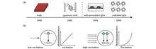
For a long time, physicists and chemists have dreamed of experimentally imaging molecular orbitals, which contain information on the spatial distribution of the electrons at a certain energy. To date, experimental methods for this purpose include femtosecond laser spectroscopy and scanning probe microscopy, which have gained widespread interest but also have some limitations. For example, high-order harmonic generation process based on ultrashort laser pulses is limited to the study of simple gas-phase molecules, and methods based on scanning probe microscopy require extremely low temperature to prevent molecular diffusion. In comparison, photoemission orbital tomography (POT) is based on angle-resolved photoemission spectroscopy (ARPES) at room temperature with less restricted experimental conditions. As a combined experimental and theoretical technique, POT focuses on establishing a direct link between the photoelectron angular distribution and the initial-state molecular orbital structure. By using a relatively simple plane-wave approximation, one can perform accurate analysis of the angle-resolved photoemission spectra for π-conjugated molecules on surface to study their respective properties.Progress Since POT deals with the photoemission experimental data, the correct description should be Dyson orbitals. Because of the fact that Dyson orbitals closely resemble one-electron Kohn-Sham orbitals calculated from density functional theory (DFT), the simple one-electron picture is often used. By approximating the final state of photoelectrons by a plane wave, it can be shown that the photocurrent arising from one particular initial state, appearing as an intensity map (so-called k-map) in momentum space, is proportional to the Fourier transform (FT) of the initial state wave function (Fig. 1). This tomographic relationship can be refined by taking two additional aspects into consideration: the first is to treat the final state with a damped plane wave in the z direction (Fig. 2), and the second is to include a modulating term of polarization-dependent geometry factor (Fig. 3). Experimentally, it is favorable to obtain a large detectable momentum-space range for the applications of POT. Suitable ARPES apparatuses include photoemission electron microscope, NanoESCA, toroidal electron analyzer, and time-of-flight momentum microscope.The accuracy and precision of the POT method have been proved by accumulating results in the past decade and several applications are introduced. Agreement between experimental ARPES results and calculated k-maps can be well utilized to determine the molecular orientation, if all orientation domains are properly considered. On the other hand, one could also infer the molecular orientations by comparing the measured k-maps with the theoretical ones based on the single molecule (Fig. 4). POT, being capable of mapping the angular distribution of the wave function for each peak in conventional photoemission spectra, is an ideal technique to unambiguously identify the energy levels of molecular orbitals (Fig. 5). If multiple molecular orbitals coexist in a small energy window, POT can provide an orbital-by-orbital characterization via deconvolution and create benchmark for ab initio electronic structure theory (Fig. 6). Efforts have also been made to regain the lost phase information of orbital in the FT process (Fig. 7) and even reconstruct the orbital in real space (Fig. 8). Quantitative studies using POT have covered topics such as intra- and intermolecular band dispersion (Fig. 9), delocalized π-states and localized σ-states, nonplanar molecules, electron-phonon coupling (Fig. 10), aromaticity, and the list continues.Conclusions and Prospects The overall experimental simplicity of POT and the convenience to approach molecular orbital and its Fourier transform under the plane-wave final state approximation are key reasons for the wide application of the technique. Albeit not applicable to some data from photoelectron diffraction and circular dichroism experiments, this approximation can provide a new perspective to study physical processes such as orbital hybridization by analyzing the discrepancy between theory and experiment. Future research on POT will improve the theoretical basis of the technique by implementing the time-dependent density functional theory (TDDFT), providing more accurate predictions of the photoelectrons’ momentum distribution. In combination with ultrafast lasers, POT has great potential to be extended into the time domain. For example, real-time observation of molecular orbitals in momentum space during excitation processes (Fig. 11) or chemical reactions will greatly improve the understanding of ultrafast dynamics. With the help of advanced momentum microscopy, such as spin-resolved ARPES and NanoARPES, it is likely to further enhance the characterization capabilities of POT in momentum and real spaces and expand its application in materials science, physical chemistry, and nanophotonics.SignificanceDevelopment of nanotechnology in the last few decades have witnessed the miniaturization of semiconductor devices and new challenges such as building a quantum computer using novel physical phenomena. On the fundamental level, however, many aspects in the understanding of physical properties at interfaces between materials are still in the exploration stage, and precise experimental and theoretical descriptions of complex surface structures are always difficult but crucial for practical applications. In the subfield of organic electronics that studies the solid-molecule interfaces, such as in organic light-emitting diode (OLED) displays or organic solar cells, the frontier orbitals of molecules are prime determinants of chemical, optical and electronic properties in the devices.
Jan. 10, 2023Vol. 50 Issue 1 0113001 (2023)
Peng Huang, Yongyou Zhang, and Haizheng Zhong
Significance Biexcitons are exciton pairs which interact via Coulomb interactions and recombine to emit two photons. Compared with single excitons, biexcitons are achieved under a high excitation intensity. The physical model of the biexciton can be simplified as two electrons at the bottom of the conduction band and two holes at the top of the valence band. The luminescence process of biexcitons involves the cascade recombination of two excitons, and the intensity of the biexcitons shows a quadratic scale as a function of the excitation intensity.Biexcitons were first observed in CuCl by Mysyrowicz et al. in 1968 and then extended to other semiconductor materials, including II-VI (ZnSe and CdS) and III-V (GaAs). In the 1980s, the study of biexcitons spread to low-dimensional semiconductors, such as quantum wells or quantum dots (QDs), resulting in the discovery of entangled photon pairs as well as predicted advances as a laser gain medium. In the last 40 years, QDs have been widely studied owing to their size-dependent optical properties and potential applications in photonics and optoelectronics. Owing to their well-known quantum confinement effects, QDs offer strong light absorption and a discrete electronic state structure. Therefore, biexcitons in QDs have unique features, including the large binding energy, correlated polarization of the emitted photons, low threshold,and enhanced temperature stability in lasing. These properties provide the advantages of realizing an on-demand entangled photon source and laser diodes.Progress The entangled photons can be generated by biexciton-exciton cascade emission or Hong-Ou-Mandel (HOM) interference from indistinguishable photons in QDs (Fig. 5). The degenerate exciton state is a superposition state and emits an exciton photon with opposite circular polarization with respect to the polarization of previously emitted biexciton photons. In 2006, Stevenson et al. demonstrated entangled photon pairs from a single InAs QD. Subsequently, InAs QDs were optimized to achieve high-quality entangled photons with reduced exciton polarization splitting. In 2019, Pan et al. performed a Boson sampling experiment using 20 pure single photons generated by a single InAs/GaAs QD. These results are significant breakthroughs in the field of quantum information and have inspired increased efforts to explore QD-based quantum light sources.In addition to the progress in self-assembled QDs, colloidal QDs have also received considerable attention because of their solution processability and easier spectral tunability. Because of the atom-like discrete structure of the electronic states in QDs, the population inversion is realized only when a fraction of QDs is excited with biexcitons (Fig. 7). The presence of biexcitons leads to an intrinsic nonradiative Auger recombination (Fig. 6). Owing to the efforts of Klimov et al., several strategies have been successfully developed to suppress Auger recombination by controlling the electronic structure of QDs. Recently, Sargent et al. used the long Auger lifetime of thick-shell CdSe/CdS QDs to realize continuous wave (CW) lasing. The observed thresholds were 6.4-8.4 kW/cm2. Klimov et al. used alloyed CdSe/CdxZn1-xSe/ZnSe0.5S0.5 QDs to fabricate a light-emitting diode architecture with a high-current focusing. This electrical pumping device shows a population inversion of the band-edge states in the absorption spectrum.Conclusions and Prospects Because biexcitons in QDs exhibit unique advantages in achieving entangled photon sources and quantum-dot lasers, exploring the photophysics of biexcitons in QDs is of great interest. Although significant progress has been made in recent years, there are still many challenges, such as increasing the number of entangled photons to enhance the quantum advantage, maintaining the high fidelity of entangled photons in long-distance transmission, and exploring new methods to suppress Auger recombination more effectively to realize electrically pumped colloid-quantum-dot lasers.
Jan. 10, 2023Vol. 50 Issue 1 0113002 (2023)
Aiwei Wang, Chi Li, and Qing Dai
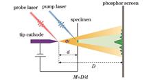
Ultrafast electron microscopy is required to realize the high temporal-spatial resolution characterization of ultrafast dynamic processes. The ultrafast transmission electron microscope (TEM) and the ultrafast scanning electron microscope (SEM) have realized the real space observation of ultrafast dynamic processes at the nanoscale and atomic levels. These processes include atomic diffusion, chemical reaction, phase change, and biological macromolecular dynamics. Ultrafast TEM and ultrafast SEM typically use high-energy (>20 keV) electron beams for imaging. However, owing to the small scattering cross-section of high-energy electrons, the detection sensitivity to the weak local electric or optical field of the sample is low. Therefore, the transient charge transport process is challenging to characterize. In contrast, low-energy electrons with energy less than 500 eV have large scattering cross-section and scattering deflection angle for the weak local electric field in the sample and transient light field on the surface of nanostructures. Moreover, characterization with spatial resolution in the order of 10-10 m can be achieved via electron holography. Therefore, when combined with ultrafast temporal-resolution technology, the low-energy electron holography is expected to characterize the local electromagnetic field distribution and charge transport at the atomic level.Point electron source projection microscope (referred to as point projection ) is the simplest device to realize low-energy electron holography. By employing the laser-pumped ultrafast electron source, ultrafast low-energy electron holography can be achieved. Because matching the complex electron optical system is not needed, there is no aberration. The spatial resolution mainly depends on the electron source coherence. Therefore, an ultrafast coherent electron source is required to achieve ultrafast high spatial-resolution holography. In the past few years, many mechanisms to generate ultrafast electrons are discovered, including photon-assisted field emission (PFE), multiphoton photoemission (MPP), above-threshold photoemission (ATP), and optical field emission (OFE). Based on these mechanisms, ultrafast coherent electron sources have been built, and high temporal-spatial resolution holography has been achieved. Therefore, the current research is essential to guide the future development of this field more rationally.Progress First, the fundamental mechanism of ultrafast electron sources is described in detail, and their coherence is discussed. The ultrafast electron source can be realized via laser pulse-modulated field emission. Photoelectron-emission mechanisms, including PFE, MPP, ATP, and OFE, generate ultrafast electron emission, which can achieve femtosecond or even up to sub-femtosecond temporal resolution. Among these mechanisms, the electrons emitted under the PFE mechanism have a low-energy dispersion equivalent to the static field emission (Table 1), resulting to high coherence. Second, low-dimensional materials, such as one-dimension carbon nanotubes (Fig. 5) and zero-dimension quantum dots, have atomic-scale curvature radii and discrete energy levels induced via quantum confinement effect, enabling the high-coherent emitted electrons. Then, the influence of laser power, laser wavelength, radius of curvature, and discrete energy levels on electron source coherence is summarized, as shown in Table 2. Lastly, the development of static and ultrafast low-energy electron holography is introduced. Furthermore, based on high-coherent tungsten tip electron sources, static holographic imaging of single protein molecule, single DNA molecule, graphene lattice, and sub-nanometer scale charge state can be achieved. Using ultrafast electron sources, the sub-10 fs temporal resolution characterization of the ultrafast dynamic process of photogenerated carriers and nanogap charge transfer in semiconductor nanowires can be realized. However, the spatial resolution of electron holography can only reach several nanometers, as shown in Fig. 10, much larger than that in the static cases. The main reason is that the thermal effect, photon energy mismatch, and strong light field acceleration caused by femtosecond laser weaken the electron source coherence, reducing the spatial resolution of the ultrafast holography.Conclusions and Prospects In conclusion, further improvement of ultrafast electron source coherence based on traditional metal nanotip is challenging owing to its physical property limitation. In contrast, low-dimensional nanomaterial electron sources, such as electron source based on carbon nanotubes, have atomic-scale emission sites and quantized discrete energy levels, which is an important basis for breaking the coherence bottleneck. Additionally, carbon nanotubes have rich carbon-chiral structures and cutting-edge quantum structures, bringing more regulatory dimensions for the optimal design of high-performance electronic sources. In the future, we will develop the optimal carbon tube emission structure by combining the atomic-scale material design based on the first principle and the bottom-up atomic manufacturing technology. This structure is expected to achieve an ultrafast electron source close to the uncertainty principle limit and promote the development of the atomic resolution of ultrafast electron holographic imaging technology.SignificanceSolar energy utilization is crucial for all life on earth. For example, photosynthesis in green plants, which is vital for humans and other living creatures to have access to food, depends on solar energy. Furthermore, solar energy is the cleanest energy source and has various other applications, including solar-electric energy conversion through photovoltaics and solar-chemical energy through photosynthesis and photocatalysis. However, the conversion efficiency is currently low and needs to be improved. Therefore, the study of ultrafast dynamic processes at the atomic scale, such as carrier excitation, photoinduced charge separation, charge transfer, and energy transfer, is crucial for revealing the underlying physical mechanisms of photosynthesis, photovoltaic, and photocatalysis, which is significant for improving the conversion efficiency of solar energy.
Jan. 10, 2023Vol. 50 Issue 1 0113003 (2023)
Zhiqiang Guan, Wei Dai, Xiuping Chen, and Hongxing Xu
The photothermoelectric effect is a photoelectric detection mechanism that uses the thermal effect generated by light and combines the thermoelectric response properties of materials to generate electrical signals. It has the advantages of zero external-bias operation, broadband optical response, and no bandgap limitation. Thus, the photothermoelectric effect has potential applications in infrared and terahertz photodetection. With the potential impact on the efficient utilization of hot carriers in nanomaterials and the demand for long-wave detection at room temperature, research on the photothermoelectric effect has rapidly advanced in recent years, with new materials and novel device designs emerging in this field. However, the mechanism, simulation, measurement methods of relevant material parameters, design guidelines, and detection performance of photodetectors based on the photothermoelectric effect still urgently need to be clarified and summarized in this field to deepen our understanding and enrich research tools.Progress Starting from the physical mechanism of the photothermoelectric effect, we systematically examined the factors influencing the photothermoelectric effect, such as the Seebeck coefficient, carrier mobility, optical absorption efficiency, and thermal properties. We reviewed the conductivity and Seebeck coefficient improvement method by adjusting the bandgap and effective mass of the carrier density of states through energy band engineering. We presented a theoretical formula and experimental method for optimizing the thermoelectric figure of merit by regulating the material selection, nanostructures, phonon spectrum, and thermal conductivity. The physical mechanism of the photogenerated carrier process was also discussed. We presented experimental differentiation methods for the photothermoelectric and photovoltaic effects (Fig. 2), clarifying the different electromotive forces and photocurrent origins. We introduced a detailed multiphysical simulation model of the photothermoelectric effect using COMSOL finite-element simulation software and discussed the critical parameters for improving the photothermoelectric response. We summarized the experimental methods for measuring the material conductivity, Seebeck coefficient, thermal conductivity, thermoelectric merit, bandgap, carrier mobility, concentration, effective mass, and carrier scattering mechanism. We reviewed the research progress in photodetectors under the photothermoelectric effect in the past three years, particularly in one-dimensional carbon nanotubes, Ⅲ-Ⅴ semiconductor nanowires, two-dimensional materials, and materials with phonon-polariton characteristics. The performance of the photodetectors based on the photothermoelectric effect is summarized in Table 1. We introduced the optical, electrical, and thermal design guidelines, critical performance parameters, and recent applications of photothermoelectric effect photodetectors.Conclusions and Prospects Photothermoelectric effect photodetectors exhibit advantages of broadband optical response, nonexternal bias, and room-temperature operating conditions. Thus, they have promising applications in the visible, infrared, and terahertz photodetector regions. The photothermoelectric effect can also be applied to photovoltaics, material characterization, spintronics, and valleytronics. Before the bright application prospect, several vital problems remain to be solved for the photothermoelectric effect, such as the response speed, synergy effect of the photothermoelectric/photovoltaic effect, and optimization of thermoelectric materials with high carrier mobility. With continual research efforts in photothermoelectric effect photodetectors, extended applications based on the photothermoelectric effect are expected.SignificancePhotodetection is essential for obtaining optical information and computation. Photothermal and photoelectric detectors are two types of detectors that are widely used because of their different utilization advantages. The advantages of photothermal detectors include their broad spectral response and the ability to function at room temperature. The disadvantages of photothermal detectors include their relatively low detection speed and efficiency compared to photoelectric detectors. Photoelectric detectors exhibit high sensitivity and rapid response, but their material bandgap limits the detectable wavelength and typically requires operation under cryogenic conditions for small photon energy. The key scientific and technological demand is to overcome the bandgap limitation of materials and achieve room-temperature light detection in mid- and far-infrared and even terahertz bands. Therefore, investigations of related materials, mechanisms, and device design principles are urgent.
Jan. 10, 2023Vol. 50 Issue 1 0113004 (2023)
Zeyu Deng, Xiaohan Yang, Jinwen Zhang, Haoran Zhao, Yihang Han, Hao Dong, and Jie Shen
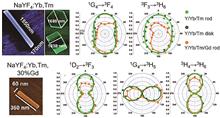
Super-resolution microscopy aims to visualize subcellular details beyond the photon diffraction limit in non-invasive and real-time ways. Rare-earth-doped upconverting nanoparticles, characterized by high photostability and large anti-Stokes shifts, have shown excellent performance in microscopy probing. So the developments in upconverting super-resolution microscopy based on recent progress in chemical synthesis and microscopy photophysics are summarized next. Jin et al. realized low-power stimulated emission depletion (STED) of highly-doped Tm3+ in a single upconverting nanoparticle and obtained an imaging resolution of 28 nm. Zhan et al. reported a multi-color upconverting super-resolution method by depleting the excitation state of upconverting sensitizer Nd3+ ions. Zhan et al. also improved the fluorescence emission difference (FED) method by using multi-core/shell upconverting nanoparticles with orthogonal excitation and emission bands. The one-scan microscopy image had a resolution of 54 nm. Schuck et al. demonstrated room-temperature photon-avalanching of a single upconverting nanoparticle pumped by a continuous wave (CW) laser for the first time. The 26th-power nonlinearity of photon-avalanching resulted in a sub-70-nm resolution under single-beam confocal scanning. Zhan et al. introduced an upconverting energy migration process into the photon-avalanching of lanthanide-doped nanoparticles, which improved avalanching nonlinearity and imaging resolution to 46th-power and 62 nm, respectively.Microlasers are promising reinforcements for integrated optical circuits, quantum physics, and bio-sensing. The major challenge of microlasers comes from energy losses in miniaturized optical cavities, which induce increasing pumping powers to reach the lasing threshold. The progress made with whispering-gallery mode micro-resonators for upconverting microlasers is summarized thirdly. Schuck et al. coupled energy-looping upconversion of Tm3+-doped nanoparticles to whispering-gallery modes of polystyrene microspheres. The coupled microsphere resonator realized CW upconverted lasing under excitation power as low as 14 kW·cm-2. Yan et al. further decreased the pumping threshold power of microsphere upconverting lasers to 4 W·cm-2. They successfully coupled the same whispering-gallery mode microsphere cavity to Yb3+/Tm3+, Yb3+/Er3+, Yb3+/Ho3+, and Yb3+/Tm3+ doped nanoparticles for multi-band lasing spanning the full visible spectrum.SignificanceRare earth (RE) doped luminescent materials are essentially important for application and research purposes due to their diverse optical properties. Rare-earth-doped upconverting materials, in particular, have piqued the majority of research interest from physics, chemistry, material engineering, biomedicine, and related fields. Photon upconversion refers to a nonlinear optical mechanism that converts two or more low-energy photons into one high-energy photon. The ladder-like energy levels rising from 4f electron configurations of lanthanide ions could stabilize both intermediate and high excited states for photon upconversion. Thus, the upconverting luminescent efficiency of lanthanide compounds could be several orders of magnitude higher than that of two-photon absorption and second harmonic generation mechanisms. Distinct from common phosphors with Stokes-shift photoluminescence, rare-earth-doped upconverting materials exhibit intrinsic anti-Stokes shifts between emission and excitation bands. It means that upconverting photon signals and background noises have little overlap in luminescent spectra. Taking advantage of sophisticated nanochemistry methods, people have prepared various rare-earth-based upconverting nanoparticles and developed upconverting luminescent probes for biomedical imaging applications. Many systematic review articles have discussed upconverting nanomaterials in aspects of structural design, chemical preparation, surface modification, biomolecular labeling, and imaging settings. The general merits of upconverting nanoparticles and related bio-probes, such as low autofluorescence and large imaging depth, are well known to multidisciplinary researchers. However, pioneer applications of upconverting materials face some new challenges, including single nanoparticle detection, multi-dimensional signal coding, novel micro-device conception, and so on. To meet these challenges, researchers need to thoroughly understand and rationally engineer the photophysics properties of nano- and micro-sized upconverting materials. Herein, we attempt to archive recent upconversion photophysics studies on rare-earth-doped materials below the micron scale. More specifically, this review article focuses on luminescent polarization, super-resolution luminescent imaging, and microcavity coupling of rare-earth-doped upconverting materials. These photophysical achievements could help our readers expand the frontier of photon upconversion applications.ProgressThe intrinsic characteristics of photon upconversion include excitation and emission wavelengths, intensity ratios of multi-bands, excited state lifetimes, and polarization. However, luminescent polarization is rarely studied, because it necessitates the use of single particle spectroscopy or collective particles in uniform self-assembly. The research achievements on upconverting polarization properties are summarized firstly. In 2013, Qiu et al. reported the polarized emission behavior of a single NaYF4∶RE nanorod. They demonstrated that the emissive polarization characteristics were determined by crystal local symmetry rather than the aspect ratio of the nanorod. Later, Qiu et al. discovered that the polarized orientation of the photoexcitation beam had a key effect on the upconverting emission intensity of a single particle. These studies established the paradigm of single particle polarized spectroscopy for upconverting materials. Researchers used polarized spectroscopy to identify the spatial orientations of upconverting particles, control their orientations via dipolar interactions, and sense local environment motions. Thus, luminescent polarization should be recognized as an important signal channel to increase the informational dimensions of upconverting materials.Conclusions and ProspectsIn this review, we discussed the photophysics studies on nano- and micro-sized upconversion materials. These photophysical discoveries in rare-earth-doped upconverting materials, such as crystal field-dependent polarization, photon-avalanching nonlinearity, and microcavity-coupled lasing, lay the groundwork for the development of new applications. However, the photon upconversion of lanthanide phosphors has not been fully unraveled at the nanoscale and beyond. We still lack tools and methods to investigate the upconversion polarization of a single nanocrystal and upconversion lasing in a nanocavity. We hope that more interdisciplinary researchers will join us to advance the related research.
Jan. 10, 2023Vol. 50 Issue 1 0113005 (2023)
Fan Yin, Jianbo De, Qing Liao, and Hongbing Fu
This review summarizes the recent research advances of biphenyl derivatives with charge transport properties and high luminescence efficiency. Approximately 20 biphenyl derivatives are introduced, including molecular design strategies and related optoelectronic properties and their application in optoelectronic devices. This review on organic conductive materials based on biphenyl derivatives with high luminous efficiency provides meaningful guidance and a material foundation for the development of organic electrically pumped lasers. This paper also briefly reviews challenges, development directions, and opportunities for the future development of the field.Progress Organic electroluminescence is a process of directly converting electrical energy into light. It occurs in organic materials where they emit light under the action of an applied electric field or current. Organic electroluminescent devices are mainly divided into two categories: organic light-emitting diodes (OLEDs) and organic light-emitting transistors (OLETs). In 1963, Pope et al. reported the preparation of the first OLED using anthracene single crystals; however, electroluminescence was only observed in anthracene single crystals with a thicknesses of 10-20 μm when the driving voltage was as high as 400 V.The construction of high-performance devices requires light-emitting materials with high mobility. In numerous literature reports, we have found that biphenyl derivatives serve as classical charge transport layers and have excellent light-emitting properties and large optical gain at the same time. In 2010, Adachi et al. reported a new type of non-heterostructure OLED device, in which BSBCz molecules are used as the emission layer (its HOMO and LUMO energy levels were 3.1 eV and 5.8 eV, respectively). They introduced two buffer layers at the ends of the emission layer with MoO3 and the metal cesium-doped BSBCz film acts as hole and electron transport interlayers. The addition of the buffer layers effectively reduces the carrier injection barrier, thereby suppressing the roll-off of electroluminescence efficiency at high current density.OLET is an integrated device that has both the switching function of an organic field effect transistor (OFET) and the light-emitting function of OLED, which can avoid complex OFET gate voltage switching to drive OLED. This can greatly simplify device fabrication and be easily integrated into display circuits. Recently, Yin et al. develop a novel 4,4'-bis (2-dibenzothiophenylvinyl)-bipheny (DBTVB) molecule based on extending the biphenyl skeleton. The introduction of dibenzothiophene groups not only extends the conjugated chain but also provides the space for the rotation of the molecular conformation to ensure the planarity of the molecule. The single crystal of this molecule exhibits a fluorescence quantum yield of up to 85% and excellent bipolar transport properties with hole and electron mobilities of 3.55 and 2.37 cm2‧V-1‧s-1. Simultaneously, this single crystal also exhibits excellent laser properties. A DBTVB-based OLET was fabricated with Au/MoO3-Ca/CsF as an asymmetric electrode. The external quantum efficiency of the device is as high as 4.03%, which is the best OLET device reported so far.Because of the rod-shaped molecular structure, the molecules tend to form a herringbone arrangement during the self-assembly process, which can effectively reduce the fluorescence quenching caused by the intermolecular π—π interaction and ensure the efficient transport of carriers. Biphenyl derivatives usually have a large Stokes shift, large transition dipole moment, and excited state oscillator strength, which ensure their good luminescence properties. Therefore, biphenyl derivatives have inherent advantages as laser gain materials. As a typical biphenyl derivative, the 4,4'-bis [(N-carbazole) styryl] biphenyl (BSBCz) molecule has very low intersystem crossing efficiency. Therefore, in the presence of oxygen, the triplet excitons generated by optical pumping are completely quenched and the triplet excited state absorption (TA) in the laser gain wavelength range is almost negligible. These advantages make it a strong candidate for realizing a continuous-wave optically pumped laser. Ren et al. reported an exciton-polariton laser based on the optical microcavity consisting of a 4,4'-bis [4-(di-p-tolylamino)styryl] biphenyl (DPAVBi) single-crystal sandwich in two layers of silver films. Such exciton polaritons can form stable macroscopic condensations at room temperature and generate lasing emission with good spatial coherence.Conclusions and Prospects The pursuit of organic electrically pumped lasers is a long-term goal that requires the joint effort of scientists in the fields of chemistry, materials science, device physics, and engineering. From the perspective of materials science, developing materials with high mobility and high luminescence properties is important for realizing organic electric pumped lasers. In this review, we summarize the reported applications of biphenyl derivatives in photoelectric devices, including OLEDs, OLETs, organic micro/nano-lasers, organic polariton laser, and organic electrically pumped lasers. The excellent photoelectric properties of these materials make them potential candidates for electrically pumped lasers.We believe that organic electrically pumped laser will be realized soon, following more and more breakthroughs in this field. The organic electrically pumped lasers can bridge the gap between current microelectronic and nanophotonic circuits to revolutionize laser displays, precision medicine, wearable devices, and information and communication technologies.SignificanceOrganic semiconductors, which combine high-efficiency light-emission and charge-transport properties, are ideal candidates for realizing organic electrically pumped lasers. However, there are still many challenges in the design and synthesis of materials with such properties. This is because of the intrinsic contradiction between high carrier transport and efficient solid-state emission efficiency in organic solids. High carrier transport requires intense molecular packing and strong intermolecular interactions; however, such interactions can significantly reduce solid-state luminescence efficiency.
Jan. 10, 2023Vol. 50 Issue 1 0113006 (2023)
Qirui Liu, Yuxiang Tang, Ke Wei, and Tian Jiang
Antiferromagnets, magnetic materials with the internal magnetic moment offset to zero, exhibit fascinating physical properties and have high application potential. First, the spin precession frequency resonant at the terahertz band of antiferromagnets has a higher spin storage density than that of ferromagnets. Second, the stray field of antiferromagnets is almost zero, which provides a strong ability to resist external interference. Third, antiferromagnets are often accompanied by many complex electronic states that give rise to some novel effects. However, owing to the characteristics of weak or zero net magnetic moments, the detection and regulation of antiferromagnetic materials have been challenging for a long time.In recent years, ultrathin and monolayer-exfoliated two-dimensional materials have provided new opportunities for research on antiferromagnets. The low-dimensional scale has improved the interaction among the lattice, electronic spin, and charge, which not only gives rise to complex and rich magnetic states but also paves the way for exploring low-dimensional magnetism and its applications by using interdisciplinary research fields such as optoelectronics. Research based on optical means has many advantages such as enabling microscopic-level, high-speed, noncontact, high-sensitivity analyses with a high space-time and high-energy resolution. In addition, it is conducive to the observation of various magnetic responses of antiferromagnets under extreme physical conditions. The developments of magneto-optical principles and optical detection technology have resulted in the use of various laser spectrum and polarization detection schemes to solve the challenges presented by antiferromagnetic material research. Therefore, it is necessary to summarize research advances on two-dimensional antiferromagnets in the existing magneto-optical field.After a brief introduction in Section 1, the basic structure, properties, and classification of typical van der Waals antiferromagnets, including chromium trihalide and transition metal phosphorus sulfide (Fig. 2), are introduced in Section 2, along with some other common materials (Table 1). Starting from different magnetic coupling characteristics (interlayer or intralayer antiferromagnetic coupling), the magnetic ordering of these antiferromagnetic materials in combination with the molecular configuration and chemical composition are reviewed.In Section 3, multiple magneto-optical effects are discussed for magnetic thin films (Fig. 3). In addition to the well-known Faraday effect, magneto-optical Kerr effect, Zeeman effect, magnetic dichroism, and Viogt and Cotton-Mouton effects, various specific magnetic changes in matters resulting from the interactions between light and matters are also included. For example, two-dimensional FePS3 exhibits giant linear dichroism because the destruction of the rotational symmetry by the antiferromagnetic order renders the electron energy band anisotropic (Fig. 4). The spin photovoltaic effect is demonstrated in multilayer CrI3, the interlayer magnetic order directly affects the magnitudes of the photocurrent and tunneling current in the direction vertical to the heterojunction. The circular polarization of the photocurrent also reveals a correlation between the magnetic state and the photon energy (Fig. 5). In terms of spectral detection, the second-harmonic emission and scattering spectra that are closely related to the magnetic order are also reviewed (Fig. 6). Subsequently, the ability of the magneto-optical effect to clearly reflect the regulation of two-dimensional antiferromagnets by means of magnetic field, electric field, temperature field, stress regulation (Fig. 7), passive regulation, and ultrafast lasers is discussed (Fig. 8).In the spectral research presented in Section 4, as a link between macro- and micro-quantum phenomena, elementary excitation quasiparticles are shown to greatly facilitate related research on low-dimensional condensed matter physics. Under antiferromagnetic conditions, the disturbance of the magnetic order may affect the properties and mutual coupling of various quasiparticles in the material. The magnons produced by the collective excitation of the laser to the spintronic system facilitate the loading of electrical information, and their frequency determines the switching speed of the spintronic devices. For applications, the energy of the magnons can be adjusted using an all-optical method and an electrostatic doping method controlled by the gate voltage (Fig. 9). On the other hand, research on the transport of magnons in two-dimensional antiferromagnetic materials has also been conducted and these transport phenomena could potentially be studied by all-optical imaging. Research on the same Bosonic excitons in two-dimensional antiferromagnets is another important research topic. The Frenkel-like excitons in CrI3 have circular-polarized and polaronic characteristics (Fig. 10), while the Wannier-like excitons in NiPS3 prefer linear polarization and high coherence in the emission spectra (Fig. 11). For another low-energy excited Bosonic phonon, strong coupling magnon-phonon states are formed through the tuning effect of a large magnetic field (Fig. 12). The dispersive anti-cross feature of this polaron state is clearly reflected in the spectra, which can provide a new research platform for the magneto-optical control of antiferromagnetic materials.Section 5 summarizes the prospects for further research and the application of two-dimensional antiferromagnets in magneto-optical and related fields.SignificanceSemiconductor microelectronics, which are based on the charge properties of electrons, have brought about revolutionary advancements to modern information technology. However, necessary improvements in the computing and information-processing capabilities of devices cannot only be achieved by manipulating and optimizing the charge properties of electrons. The manipulation of electronic spins, one of the most basic characteristics of magnetic materials, has enabled magnetic devices to become considerably successful, resulting in a series of cutting-edge applications with the advantages of nonvolatility and low-calorie requirements.ProgressThis paper reviews the progress in the field of magneto-optical research pertaining to antiferromagnets from the perspectives of optical characterization and regulation. After introduction of the basic principles, the main research objects of the interactions between laser and two-dimensional antiferromagnets are extended to the forms of the macroscopic magneto-optical effect and microscopic elementary excitation quasiparticle, respectively.Conclusions and ProspectsCompared with ferromagnets, the unique advantages of antiferromagnets in magneto-optical research are undoubtedly expected to accelerate research in spintronics-related fields. Research on antiferromagnets based on the magneto-optical effect is foreseen to focus on more complex and extreme systems in non-collinear, helical, topological, multiferroic, spin-liquid magnetic states, etc. The control of these magnetic states would enable interlayer electronic coupling to be effectively adjusted to facilitate the detection, manipulation, emission, and tracking of spin information through optical means. This approach could introduce huge optical nonlinearity, efficient spin filtering, high conversion efficiency between charge current and spin current, high electron mobility, long spin diffusion length, and other characteristics, and expand the research scope of magnetism, photonics, and other interdisciplinary disciplines. Although the ability to conduct antiferromagnetic writing and reading under two-dimensional conditions would also need to be fundamentally improved, future breakthroughs in two-dimensional antiferromagnetic opto-spintronics can certainly be anticipated.
Jan. 10, 2023Vol. 50 Issue 1 0113007 (2023)
Yuxuan Ke, Yingqian Cen, Dianyu Qi, Wenjing Zhang, and Qing Zhang
Emerging two-dimensional (2D) materials, including graphene, transition metal dichalcogenides, black phosphorus, and perovskites, have attracted considerable attention owing to their extraordinary physical and chemical properties. They are atomically thin, with no surface dangling bonds, good electrostatic tunability of carrier concentration, and strong light-matter interactions. These advantages make them promising materials for high-efficiency nanoscale photodetectors for optical chips. For instance, monolayer molybdenum disulfide (MoS2) can absorb 10% of light due to a large absorption coefficient of 107 m-1. Platinum diselenide (PtSe2) possesses high mobility of over 103 cm2·V-1·s-1 and a bandgap of 0.3-2.0 eV, which is promising for wide-band optical communication photodetectors. Meanwhile, the non-dangling surfaces of 2D materials enable van der Waals (vdWs) integration for various heterostructures without the constraint of crystal lattice mismatching.2D material photodetectors for optical communication, including single-element 2D materials, double-element 2D materials, and 2D heterostructures, have been extensively explored. They have demonstrated excellent performance, including high responsivity and detectivity, fast response time, and wide bandwidth. Despite the realization of these great successes, 2D photodetectors operating in optical communication bands still face many application challenges. Therefore, it is necessary to summarize the research progress and discuss the challenges of this important field.For double-element 2D material photodetectors, higher responsivities were achieved than those of single-element photodetectors. For instance, Leuthold's group fabricated few-layer MoTe2 waveguide photodetectors with high responsivity (0.4 A/W), broad bandwidth (1 GHz), and fast data transmission rate (1 Gbit/s) using a graphene/MoTe2/Au structure. Zhai's group achieved Bi2Se3 photodetectors with high responsivity (2.7 A/W) and detectivity (3.3×1010 cm·Hz1/2·W-1) at the C-band. For 2D heterostructures, Park's group demonstrated ReS2/ReSe2 photodetectors with ultrahigh responsivity of 1.58×10⁵ A/W at the O-band. Zhang's group demonstrated GaTe/InSe photodetectors with a broad detection range (400-1600 nm) and high responsivity (2 A/W). Furthermore, Miao's group fabricated photodetectors with a broad detection range (400-1600 nm), high detectivity (11.7 A/W), and rapid response time (30.3 μs) using MoS2/graphene/WSe2 heterostructures. Finally, the challenges and ongoing research in this field are discussed, including scalable synthesis, low Schottky barriers for electrical contact, and high absorption.SignificancePhotodetectors that convert a light signal into an electrical signal play an important role in optical communications, displays, and other such applications. Nanoscale photodetectors operating in the optical communication band are one of the most important research objects in optical chip technology. Optical communication bands contain two spectral ranges. One is called the 850 nm band from 770 nm to 910 nm; the photodetectors in this band mainly use technologically important Si semiconductors as photoactive materials. The other range includes the original (1260-1360 nm, O), extended-wavelength (1360-1460 nm, E), short-wavelength (1460-1530 nm, S), conventional (1530-1565 nm, C), long-wavelength (1565-1625 nm, L), and ultra-long-wavelength (1625-1675 nm, U) bands. The photodetectors in these bands use indium gallium arsenide (InGaAs) and mercury cadmium telluride (HgCdTe) as photoactive materials. However, they still suffer from complex and high-cost growth processes, low detection efficiency, and low operation temperature.ProgressWe first introduced the working principles and important characteristic parameters of photodetectors. The working principles include the effects of photoconductive, photovoltaic, photogating, and photo-thermoelectric properties. The characteristic parameters include the photocurrent, ON/OFF ratio, external quantum efficiency (EQE), and detectivity. Next, we discussed the research progress in photodetectors based on the 2D materials (single-element and double-element) and their heterostructures in optical communication bands (Table 1). For example, Avouris's group demonstrated a graphene photodetector with a 10 Gbit/s data transmission rate using the asymmetric metal contact technique. Xu's group demonstrated a graphene photodetector on silicon with high responsivity owing to the prolongation of the photon-generated carrier lifetime induced by the built-in field at the heterointerface between graphene and silicon. Mueller et al. demonstrated a graphene photodetector with ultrashort intrinsic response time of 2.1 ps using metal-graphene-metal structures. Javey's group designed optical cavity-enhanced tellurium photodetectors exhibiting a high responsivity (>2.5 A/W) within the entire optical communication bands (Fig. 4). Similarly, Song et al. fabricated bismuth-based photodetectors with high responsivity (0.62 A/W) and EQE (50%) at C band using photonic crystal-enhanced structures (Fig. 5).Conclusion and prospects2D material photodetectors have shown high responsivity and detectivity, fast response time, and wide bandwidth. This provides an effective strategy for the development of high-efficiency nanoscale photodetectors for next-generation optical chips and interconnections. We reviewed the recent progress made in 2D material photodetectors for optical communications. We focused on two types of material platforms: 1) 2D materials, including single- and double-element 2D materials, and 2) 2D heterostructures. Despite great progress, some challenges still exist for our ongoing exploration.
Jan. 10, 2023Vol. 50 Issue 1 0113008 (2023)
Yuexing Xia, Shuai Zhang, Keming Wu, Yiyang Gong, Shuai Yue, and Xinfeng Liu
In recent years, two-dimensional (2D) materials have attracted extensive interests due to the large exciton binding energy different from bulk materials. Many peculiar properties have been discovered that have far-reaching perspectives in the next generation of optoelectronic devices. In this review, we introduce the forms of exciton existence in 2D materials and several promising 2D materials with good applications at first. Then, we summarize relevant contemporary tools for probing exciton dynamics and methods of regulating 2D exciton transport, for instance, electrical regulation, stress/surface wave regulation and moiré potential regulation, etc. Finally, we conclude the general development of regulation in 2D materials and propose several possible opportunities of application prospect.In recent years, two-dimensional (2D) materials have attracted extensive interests due to the large exciton binding energy different from bulk materials. Many peculiar properties have been discovered that have far-reaching perspectives in the next generation of optoelectronic devices. In this review, we introduce the forms of exciton existence in 2D materials and several promising 2D materials with good applications at first. Then, we summarize relevant contemporary tools for probing exciton dynamics and methods of regulating 2D exciton transport, for instance, electrical regulation, stress/surface wave regulation and moiré potential regulation, etc. Finally, we conclude the general development of regulation in 2D materials and propose several possible opportunities of application prospect.
Jan. 10, 2023Vol. 50 Issue 1 0113009 (2023)
Yuanfei Hu, Junrong Zheng, Enming You, and Songyuan Ding
Progress We first introduce the dielectric function of UTMFs to understand their optical properties. The dielectric function of the UTMFs can be described by the Drude model; however, the intrinsic plasmon frequency and inelastic scattering rate need to be corrected.Conclusions and Prospects The key point in preparing continuous UTMFs is to suppress the island growth of the metal films on the substrate in order to reduce the percolation threshold. Current developments have achieved 1.84 nm thick continuous ultrathin gold films. Further efforts are required to improve the scalability of large-scale UTMFs. Moreover, the relationship between the processing and the corresponding properties is a fundamental scientific issue that requires further investigation.It would be interesting to prepare nanotailored UTMFs for further study of nano-optical properties in the infrared region. Moreover, the ultrathin nature of UTMFs makes it possible to integrate with nanophotonic waveguides for chip-scale applications of integrated nonlinear optics. As an emerging quasi-two-dimensional material, it has a broad scope in terms of preparation, properties, and applications. With continuous advances in the preparation process, thinner, flatter, and larger-scale UTMFs are expected to be prepared in the future. The unique properties of ultrathin metal films and their applications are also worthy of investigation.SignificanceWhen the thickness of the metallic film is reduced to the nanoscale level, ultrathin metal films (UTMFs) exhibit properties that are remarkably different from those of bulk metals, such as stronger surface plasmons and nonlinear optical responses. However, research progress in this field is slow because of the difficulties in preparing continuous UTMFs owing to the dominant island growth mode of metal thin films at the early stage of growth. With the methods proposed in recent years, such as the seed layer method, organic modification method, co-deposition method, and cryogenic deposition method, researchers have prepared continuous metal films with thicknesses of a few nanometers and found that they have many novel optical properties, such as broadband absorption in the infrared, electrically tuned surface plasmon, and strong nonlinear optical response.Four growth methods for the preparation of continuous UTMFs are highlighted and comparedthe seed layer method, organic modification method, co-deposition method, and cryogenic deposition method. The seed layer method involves pre-depositing a layer of material (usually using transition metals such as titanium and chromium) with a thickness of 1-2 nm on the substrate as an adhesion layer, which can improve the wettability of the metal on the substrate. The organic modification method usually modifies a layer of silane with specific groups on the substrate, thus increasing the adhesion between the metal and substrate and inhibiting island growth. The co-deposition method involves the preparation of metal films by depositing small amounts of metals such as Al, Ni, Cu, Ti, and Cr on the substrate in a doping-like manner with the target metal at the same time. In contrast, the cryogenic deposition method uses a low-temperature substrate to limit the migration of metal atoms, enabling the preparation of ultrathin metal films without seed layers.UTMFs have many unique optical properties and applications1) The resonant wavelength of the surface plasmon red-shifts as metal films become thinner. Moreover, the surface plasmon frequency of ultrathin metal films can also be electrically tuned, as its body charge density is significantly lower than that of its thick metal film counterpart. 2) The real and imaginary parts of the refractive index of the UTMFs are approximately equal in the mid- and far-IR regions. When its impedance is 188, the impedance matching condition is satisfied, resulting in wavelength-independent broadband absorption (50%). 3) The confining effect in UTMFs quantizes the free electrons of the metal into multiple subbands. Further, the dipole transit moment between the subbands is the individual electron charge multiplied by several nanometers, which is much larger than that of traditional nonlinear crystals. 4) UTMFs have excellent electrical conductivity and mechanical flexibility as well as high transmittance in the visible band, making them suitable for replacing ITO as a flexible transparent conductive material.
Jan. 10, 2023Vol. 50 Issue 1 0113010 (2023)
Lu Liu, Yupeng Wang, Yunxiu Ma, Guogang Li, and Zhigao Dai
Progress In this paper, firstly, the theory for hyperbolic PhPs is described. In the equation of dispersion and dielectric constant, it can be concluded that the hyperbolic propagation originates from the different dielectric constant. In addition, the angle between the edge orientation and the crystallographic direction significantly affects the optical response, and serves as a key tuning parameter in tailoring the polaritonic patterns. Secondly, the hyperbolic PhPs propagation characteristics including the focusing, tunability, and optical topological transformation, are discussed. These exotic properties pave the way for the nanophotonic device. Thirdly, we conclude and outlook the development of in-plane hyperbolic PhPs. With the ability of locally controlling light at the nanoscale, it can be expected that the in-plane hyperbolic PhPs have a broad prospect in nanophotonics.Conclusions and Prospects In this work, we summarize the propagation characteristics of in-plane hyperbolic PhPs based on natural metamaterials. We demonstrate that the relationship between the dielectric constant and dispersion of in-plane hyperbolic PhPs and the angle between the edge orientation and the crystallographic direction are key parameters for achieving in-plane hyperbolic PhPs. The methods to realize reflection, diffraction, focusing, optical field enhancement, and optical topological transformation of in-plane hyperbolic PhPs are summarized. This work can promote the theory and technology development of PhPs in nanophotonics.The research of in-plane hyperbolic PhPs based on natural metamaterials is still in its infancy. At present, the tunable propagation of in-plane hyperbolic PhPs has made some progress. Some optical devices such as focusing lenses, prisms, and gratings have been realized. However, it is still at the beginning stage of a single optical device function. More complex and multi-functional optical systems are required. In addition, the currently reported natural in-plane hyperbolic metamaterials are mainly α-V2O5 and α-MoO3, in which the PhPs spectra are in the infrared band. The in-plane hyperbolic PhPs in other bands are needed. Therefore, more natural metamaterials need to be discovered to realize the application of multi-band in-plane hyperbolic PhPs and nanophotonics.SignificancePhonon polaritons (PhPs) can strongly confine the free-space light field deeply below the incidence wavelength. In comparison with the well-documented metallic plasmon polaritons, PhPs can achieve improved light confinements, significantly reduced optical losses, and much higher quality factors. These characteristics enable a wealth of potential applications, such as sensing, thermal management, and ultramicroscopy. Recently, hyperbolic PhPs in thin slabs of the van der Waals materials have been intensively investigated as they exhibit extreme field confinement and exotic ray-like propagation, with potential for hyperlensing and focusing of mid-infrared light at the nanoscale. However, hyperbolic PhPs exhibiting out-of-plane hyperbolic propagation limits the development of hyperbolic nano-optics compatible with on-chip optical devices. In this regard, hyperbolic PhPs with in-plane propagation have recently been demonstrated in artificial metasurfaces and in the natural van der Waals crystals α-V2O5 and α-MoO3. Compared with the complex photolithography technology from artificial metasurfaces, the natural metamaterials have great prospects in planar configuration nanophotonic devices. Hence, this work reviewed the research progress of in-plane hyperbolic PhPs based on natural layered metamaterials in recent years.
Jan. 10, 2023Vol. 50 Issue 1 0113011 (2023)
Siyuan Wang, Hongyao Liu, Xinchao Lu, and Chengjun Huang
Nanopores provide a sensing volume comparable to the size of single molecules, which is conducive to realize single-molecule detection. Early nanopore-based sensors mainly depend on electrical measurements, single-molecule detection in nanopores using optical methods has recently emerged as an alternative approach. In this context, plasmonic nanopores have been proposed and extensively investigated. Plasmonic nanopores combine plasmonic nanoantennas with nanopores, which confine and enhance optical excitation near the nanopores, forming hotspots that have significant advantages for single-molecule sensing. First, the strong electromagnetic field enhances the interaction between the field and the single molecule in the hotspot, while reduces the noise generated by molecules at other locations. Second, the gradient electric field in the plasmonic nanopore attracts nearby molecules, increasing the molecular translocation time. Third, the refractive index distribution of the plasmonic nanopore directly affects the resonance conditions, which constitutes the molecular information in the hotspot. Therefore, plasmonic nanopores have been increasingly explored for single-molecule detection in recent years.With the development of single-molecule optical detection based on plasmonic nanopores, diverse plasmonic nanopore structures and measurement schemes have been proposed to detect a variety of single molecules, which renders a review of the existing studies necessary.Progress In this review, the typical structures of plasmonic nanopores and their mechanisms of field enhancement, the mostly used detection strategies, the application progress, and typical achievements in single-molecule detection are described.Section 2 summarizes the classification and typical structures of plasmonic nanopores. Plasmonic nanopore structures can be divided into three types: plasmonic nanopores based on metal micro/nanostructures (including plasmonic nanowell-nanopore, plasmonic nanoslit cavity, and plasmonic bullseye structures), plasmonic nanopores based on nanogaps (including bowtie nanoantennas, double nanoholes, and nanoparticle dimers), and plasmonic nanopores based on glass nanopipettes (including gold nanoporous spheres and thin-film-modified single nanopores). The structure characteristics and field enhancement mechanisms of each plasmonic nanopore structures are discussed.Section 3 describes the four mostly used detection strategies for plasmonic nanopores and their characteristics, including fluorescence detection, surface-enhanced Raman spectroscopy (SERS), surface plasmon resonance displacement sensing, and combined optical and electrical sensing. Fluorescence detection is one of the most widely used methods for the detection of single molecules in solution. Plasmonic nanopores significantly amplify the fluorescence signal and decrease background noise. However, the introduction of fluorescent dyes may affect the molecular state of single molecules, increasing the experimental complexity. The development of label-free single-molecule detection strategies such as SERS and plasmonic resonance displacement sensing is highly desired. Meanwhile, combined optical and electrical sensing is expected to break the current bottleneck of electrical signal detection in solid nanopores, enabling single-molecule sensing with high signal-to-noise ratio and high resolution.Section 4 provides a brief review of the application progress and typical achievements of plasmonic nanopores in the detection of single molecules including DNA, proteins, peptides, and other bioparticles. The detection of DNA molecules mainly includes DNA molecular translocation, DNA identification, and gene sequencing. Plasmonic structures such as bowtie nanoantennas, bullseyes, and plasmonic nanowells-nanoholes have been used for the translocation detection of single DNA molecules, and the optical label-free detection of single DNA molecules has been achieved using plasmon resonance displacement sensing. DNA identification and sequencing processes are mainly based on SERS signals. Due to the weak spectral signals of single DNA molecules, plasmonic nanopores providing larger field enhancement are preferred for SERS detection. The detection of proteins and peptides involves capture, identification, and structural characterization. In addition to the detection of biological single molecules, plasmonic nanopores are used for the detection of bioparticles such as bacteria and viruses.Section 5 summarizes the opportunities and challenges for further research and application of plasmonic nanopores.Conclusions and Prospects Plasmonic nanopores realize nanometer-sized hotspot fields near the nanopores, enhance the interaction between the field and matter, and achieve highly sensitive detection with high spatial resolution. In recent years, plasmonic nanopores have been increasingly explored for the optical detection of single molecules. Optical detection offers many advantages over electrical sensing strategies, such as decoupling of the driving voltage and buffer conditions from the signal strength and big-bandwidth data acquisition. As one of the most promising optical strategies, SERS based on plasmonic nanopores provides compositional information on the detected substance. Extending the residence time of the detected substance near the nanopores is the main challenge to realize plasmonic-nanopore-based SERS. This is currently achieved through the optical force of plasmonic nanopores. Although some progress has been reported, it is still necessary to develop multiphysics coupling models to achieve a more controllable and stable three-dimensional manipulation of molecules. Combining optical and electrical sensing strategies in plasmonic nanopores has also great potential for superior single-molecule detection. Plasmonic nanoantennas optimize the performance of electrical measurements by increasing the molecular translocation time and enhancing electrical signals. Further development of the above technologies will promote the plasmonic nanopore technology for single-molecule detection and identification and realize the single-molecule sequencing technology.SignificanceSingle-molecule detection promotes the development of biological research because it reveals details that remain concealed to ensemble measurements. However, the detection and analysis of single molecules confront great challenges. On the one hand, single molecules produce very weak signals, requiring extremely sensitive detection methods. On the other hand, the sizes of single molecules are mainly confined to the nanoscale and they move with the naturally random state. It is necessary to isolate the detected signal of the target molecule and exclude interferences from other molecules. Therefore, the development of single-molecule detection methods attracts considerable researchers attention.
Jan. 10, 2023Vol. 50 Issue 1 0113012 (2023)
Fengsheng Sun, Zebo Zheng, Wuchao Huang, Ningsheng Xu, Ximiao Wang, Tianwu Wang, Huanjun Chen, and Shaozhi Deng
Results and Discussions In the theoretical model, the vdW heterostructure is modeled as a 2D infinite waveguide (Fig. 1). The thicknesses of top (ε^[1]) and bottom layers (ε^[2]) are d1 and d2, respectively. It is sandwiched between two semi-infinite plates, which act as the substrate (εs=ε[3]) and cover layer (εc=ε[0]). The electromagnetic modes [Eqs. (S8)-(S10), Supporting materials] and the associated polariton dispersions [Eq. (4)] are obtained by solving the Maxwell’s equations upon the continuities of the electric and magnetic fields at interfaces. With the input of dielectric functions of monolayer graphene [Eq. (2)] and α-MoO3 [Eq. (1)], the calculated polariton dispersions and contours of the α-MoO3/Gr heterostructure are shown in Fig. 1 and Fig. S4 in the Supporting materials. In comparison with the pristine monolayer graphene and α-MoO3 lamina, due to the isotropic plasmon polariton in the graphene, the dispersion contours of the heterostructure are more complex and distorted along the [100] and [001] directions. Therefore, the hybridized plasmon-phonon polaritons can propagate along these directions that are forbidden respectively for the phonon polaritons in Restrahlen Band 1 and Band 2 in α-MoO3 lamina (Fig. 2). The theoretical results are further corroborated by numerical simulations using FEM (Figs. 1 and 2) and experimental nano-imaging measurements (Figs. 3 and 4). Moreover, the influence of the thickness of α-MoO3 lamina on the polariton hybridizations in α-MoO3/Gr heterostructure is also investigated. Because the polariton fields are of evanescent nature, by reducing the α-MoO3 thickness, the hybridized polaritons converge to the plasmon polariton in monolayer graphene, while with the increase in the α-MoO3 thickness, the polaritons in the heterostructure evolve into the phonon polaritons in the pristine α-MoO3 (Fig. 4). The results are also corroborated by the nano-imaging measurements (Fig. 4).ObjectiveTwo-dimensional (2D) van der Waals (vdW) crystals like graphene and α-MoO3 can support polaritons in the spectral range from terahertz to mid-/far-infrared regime, enabling nanoscale confining, focusing, and controlling of the electromagnetic fields. The hybridization between different polaritons can further enrich the properties of polaritons and bring more degrees of freedom for the regulation of electromagnetic fields at the nanoscale. In this paper, we studied the hybridization of plasmon polaritons and phonon polaritons in a heterostructure composed of an α-MoO3 vdW thin lamina stacking onto a monolayer graphene. An analytical waveguide model was developed to calculate the polariton propagation characteristics in the vdW heterostructure. The dispersion contours, dispersion relations, and localized electromagnetic field distributions of the hybridized polariton waveguide modes were derived. The theoretical results were then verified by real-space optical nano-imaging and numerical simulations. Our study can provide a quantitative model for the calculation of the hybridized polariton waveguide modes in vdW heterostructures, which can help further exploring the interactions between different types of polaritons in 2D vdW crystals.MethodsIn our theoretical model, the vdW heterostructure is treated as a 2D infinite waveguide supported onto SiO2 substrate, which consists of a monolayer graphene of 0.5-nm thickness and an α-MoO3 lamina of 115-nm thickness (Fig. 1). The dielectric functions of the graphene and α-MoO3 are described using the Drude model and Lorentz model, respectively. Because in α-MoO3 the polaritons can approximately be treated as transverse magnetic (TM) mode, the electromagnetic modes and the associated dispersion relations of the heterostructure can then be obtained by solving the Maxwell’s equations upon the continuities of the electric and magnetic fields at interfaces. Monolayer graphene was grown by the chemical vapor deposition (CVD) method. Microfabrication technique combining electron beam lithography (EBL) and reactive ion etching (RIE) was employed to pattern the graphene into microstructures. The vdW α-MoO3 laminas were grown using a physical vapor deposition method. Dry transfer method was utilized to prepare the α-MoO3/graphene (α-MoO3/Gr) heterostructures, where the monolayer graphene microstructures were covered with α-MoO3 laminas of different thicknesses. Real-space nano-imaging was conducted using a scattering-type scanning near-field optical microscope (NeaSNOM, Neaspec GmbH, Germany). In a specific measurement, a metal-coated tip (Arrow-IrPt, Nanoworld, Switzerland) was illuminated using a mid-infrared laser (Access Laser, USA) with a wavelength range of 9.20-10.70 μm (934.5-1087.0 cm-1). The tip was vibrated vertically with a frequency of about 280 kHz. The backscattered light from the tip was detected in a pseudo-heterodyne interferometric manner, where the scattered light was demodulated at the fourth harmonic of the tip vibration frequency. The optical and morphological images of the sample can be simultaneously obtained by scanning the heterostructure underneath the tip. For the numerical study, the real-space polariton waves were manifested as the real-part of the z-component of the electric field, Re(Ez), on the surface of the SiO2 substrate. They were calculated using the finite element method (FEM) simulations (COMSOL Multiphysics). A vertically-polarized electric dipole source was fixed above the α-MoO3 with a separation of 50 nm (Fig. S5, Supporting materials). The thicknesses of the air, α-MoO3, graphene and SiO2 layers were 500 nm, 115 nm, 0.5 nm and 500 nm, respectively. The permittivities along the three principle axes were calculated according to Eq. (1). The anisotropic dielectric tensors of the α-MoO3 layer are written as ε^=[εx, 0, 0; 0, εy, 0; 0, 0, εz] and ε^=[εxx, εxy, 0; εyx, εyy, 0; 0, 0, εzz]. These tensors were imported into the COMSOL package to solve the Maxwell’s equations. For the monolayer graphene and α-MoO3 lamina, the Re(Ez) was monitored respectively on the planes 5 nm away from their upper surfaces, while for the α-MoO3/Gr heterostructure, the Re(Ez) was monitored on the plane 4 nm away from the graphene upper surface.ConclusionsIn conclusion, we have established a theoretical model to investigate the hybridizations of plasmon polaritons and phonon polaritons in a heterostructure consisting of an α-MoO3 lamina covering a monolayer graphene. The propagation characteristics, including the polariton dispersion relation, in-plane dispersion contour, and localized electromagnetic field distribution, were calculated and studied. It is revealed that due to the hybridization effect, the α-MoO3/Gr heterostructure is able to support polariton propagation along the directions that are forbidden for the phonon polaritons in pristine α-MoO3 lamina. Additionally, the influence of the α-MoO3 thickness on the polariton hybridization in the heterostructure was also investigated, indicating that when the α-MoO3 lamina was thinner/thicker, the hybridized polaritons became more plasmon/phonon polariton-like. The theoretical results were corroborated respectively by the numerical simulations and experimental nano-imaging measurements. We strongly believe that the results obtained in our study can on one hand provide a theoretical model for analytically studying the polariton hybridizations in vdW heterostructures, and on the other hand help further our understanding on the polaritonic physics in low-dimensional materials.
Jan. 10, 2023Vol. 50 Issue 1 0113013 (2023)
Yuanyuan Li, Longkun Yang, and Zhipeng Li
Results and Discussion The experimental results show different polarization correlations between the excitation and emission of the nanowire-triangular plate coupled structure. The emission polarization follows the direction of the excitation polarization. Meanwhile, the emission polarization is maintained at 160°, regardless of the incident polarization. In the simulation, we recorded the local near-field distribution and obtained the corresponding far-field emission using the FDTD method. When the triangular plate-nanowire coupling exhibits a “line” connection, the emission polarization increases monotonically with the incident polarization. However, when the coupling type exhibits a “point” connection, the emission polarization remains at 160°, regardless of the incident light. These experimental and simulation results show that the emission behaviors can be effectively modulated by the wire-triangular plate coupling type. To elucidate the modulation mechanism, we analyzed the plasmon modes excited in the nanowire-triangular plate junction. The three modes contribute to the emission from the junction: hybridized wire modes m=0 and m= 1 and the nanowire-triangular plate coupling mode P (Fig. 5). Based on antenna radiation theory and the volume integration of the free current density, we calculate the emission contributed by the triangular plate and nanowire. The results show that the light emitted from the triangular plate is always polarized at 160°, regardless of the incident polarization. It can be understood by the fact that the orientation of induced dipole oscillation is 160°. In addition, the emission polarization from the wire part is the same as the incident polarization. Hence, when the triangular plate-nanowire exhibits “wire” coupling, the junction serves as a Fabry-Perot cavity and the wire modes dominate the emission polarization rotating with the incident polarization. When the triangular plate-nanowire exhibits a “point” connection, the near-field is mainly localized on the triangular plate, in which the emitted light dominated by coupling mode P with polarization remains in the 160° orientation.ObjectiveSurface plasmon polaritons (SPPs) supported by metallic nanostructures can confine electromagnetic fields at the nanoscale and overcome the diffraction limit. Compared with conventional electronic devices, integrated subwavelength optical devices with high data transmission rates and wide bandwidths provide a promising platform for the development of nanophotonics. In recent decades, various plasmon-based optical elements have been developed, including waveguides, resonators, nanoantennas, multiplexers, and switchers. Polarization-controllable optical elements are important in chip-to-chip interconnects, sensors, and quantum cryptography. Chemically synthesized nanowires have been reported to function as polarization-controllable plasmonic waveguides, where the emission of different SPPs modes relies on the shape of the wire end. Additionally, optical properties sensitive to incident polarization have been observed in coupled nanostructures composed of wires or nanoparticles. For example, the near-field enhancement and far-field emission polarization of coupled junctions can be modulated via incident polarization, through which polarization-dependent routers, modulators, and logic gates have been achieved. Hence, further optimization of coupled waveguides can provide additional flexibility for controlling light polarization at the nanoscale. In this study, we investigated the correlations between the emission and incident polarization of a nanowire-triangular plate coupled structure. The results indicate that the polarization dependence can be modulated by the wire-triangular plate coupling type. The response of the emission polarization to the incident polarization is verified using the finite-difference time-domain (FDTD) method. In theory, by calculating the volume integration of the free current density, the conversion of propagating SPP modes and wire-triangular plate coupled mode can be revealed. The emission mechanism of the coupled structures can be elucidated based on the superposition of different SPP modes. The findings provide a new degree of freedom for manipulating light polarization at the nanoscale, and are beneficial to the development of plasmonic nanophotonics.MethodsIn this study, we fabricated silver nanowire-triangular plate coupled structures using a typical chemical method. A dilute ethanol suspension comprising nanowires and triangular plates was drop-cast onto an indium tin oxide-coated glass slide, where the coupled structures were self-assembled after drying under ambient conditions. Scanning electron microscopy was used to distinguish the different coupled structures, as shown in Figs. 2(a) and 3(a). Subsequently, the samples were immersed promptly in an index-matched oil with n=1.518 to protect the samples against oxidization or sulfuration in air. Next, optical measurements were performed, where He-Ne laser with a wavelength of 633 nm was focused onto the nanowire end through an oil objective. The response of the emission polarization to the incident polarization was obtained by rotating the half-wave plate and polarizer. The experimental data were verified via simulation using the FDTD method, and the emission mechanism was determined by calculating the volume integration of the free current density.ConclusionsWe fabricated silver nanowire-triangular plate coupled structures via wet chemical synthesis and investigated their polarization correlations between incident light and emission. The results showed that the incidence-emission polarization correlation depended on the coupling type of the nanowire-triangular plate. When the triangular plate-nanowire exhibited a “line” connection, a Fabry-Perot cavity was formed in the junction. The polarization of the emitted light followed with the excitation polarization.However, for the “point” coupling type, the emission polarization remained at 160°, regardless of the incident polarization. The emission mechanism can be interpreted by the superposition of propagating SPP modes and the localized mode of the coupled nanowire-triangular plate structure. Hence, the emission polarization at the junction can be manipulated by the nanowire-triangular plate coupling type. These findings can be used to develop more sophisticated polarization-controllable devices and are beneficial to the development of integrated nanophotonics.
Jan. 10, 2023Vol. 50 Issue 1 0113014 (2023)
Haoran Long, Yuan Gao, Hao Liu, Kaiyao Xin, Yali Yu, Juehan Yan, and Zhongming Wei
ObjectiveUltraviolet (UV) detectors are a new detection technology developed after infrared and laser detection technologies. Compared with infrared detectors, UV detectors have a higher signal-to-noise ratio because they are not affected by environmental heat sources. Thus, UV detectors have potential value and development prospects in many fields, including optical communication, medical treatment, electronics, and fire warning. Two-dimensional materials have been widely studied in the field of photodetectors in recent years owing to the absence of dangling bonds on the surface, interlayers linked by van der Waals forces, and no lattice mismatch when constructing heterojunctions. However, research on UV photodetectors based on two-dimensional materials is faced with the problems of few wide-bandgap two-dimensional materials and poor detector performance, particularly slow response speed. This work reports the energy band structure and optical absorption characteristics of a novel wide-bandgap two-dimensional semiconductor, TlGaS2. A UV photodetector based on a TlGaS2 nanosheet is fabricated. The detector exhibits a clear response from the UV to solar-blind UV spectral regions, lower dark currents, and faster response speeds. We hope that our research can broaden the wide-bandgap two-dimensional material system, and provide new ideas and methods for the realization of high-performance two-dimensional material UV photodetectors.MethodsIn this study, tapes are used to mechanically exfoliate TlGaS2 single crystals into nanosheets, which are dry-transferred onto SiO2/Si substrates using polydimethylsiloxane (PDMS). The structure and chemical composition of the nanosheets are determined via Raman spectroscopy and X-ray photoelectron spectroscopy (XPS). The morphology and thickness of the nanosheets are characterized using atomic force microscopy, and the spectral absorption range of the material is determined using an absorption spectrum test. The energy band structure and density of states of the TlGaS2 material are calculated by first principles to determine its energy band structure, which uses density functional theory (DFT) theory with projector augmented-wave (PAW) pseudopotentials and a hybrid functional. The obtained TlGaS2 nanosheets are fabricated into devices via a lift-off process using electron beam lithography and electron beam evaporation to obtain patterned two-terminal electrodes. The optoelectronic properties of the fabricated detector devices are tested using a semiconductor tester under laser irradiation or a mercury lamp with an added filter.Results and DiscussionsAccording to the first-principle calculation [Fig. 2(a)], TlGaS2 is an indirect bandgap semiconductor, and the valence band maximum is located at the Γ point. The bandgap width is 2.59 eV, and there is also a direct bandgap of 2.76 eV at the Γ point. The calculated results are consistent with the absorption spectrum test results for the material [Fig. 2(c)]. The TlGaS2 nanosheets absorb energy near 480 nm (2.6 eV) through an indirect transition, and there is a transition from indirect to direct near 430 nm (4.85 eV), which shows a steep absorption edge. At the same time, the absorption spectra show that TlGaS2 has high absorption in the UV region, even in the solar-blind UV region. The UV photodetector based on mechanically exfoliated TlGaS2 nanosheets forms a good ohmic contact with the Ti/Au electrode. The photoelectric test (Fig. 3) shows that the detector s dark current is on the order of 10-13 A. It has a certain response to optical signals smaller than 480 nm, and the steep increase in the photocurrent from 430 nm is consistent with the change trend of the absorption spectrum of the material. The detector exhibits an obvious photoresponse in the entire UV band. The best performance is achieved at 360 nm, with a responsivity of 57 mA/W and a detection rate of 2.69×1010 cm·Hz1/2·W-1. A transient test shows that the detector has a relatively fast response speed. After testing [Fig. 4(a)], the TlGaS2 detector shows the on-state response time of 51.8 μs and the off-state response time of 45.1 μs. In addition, the detector exhibits a good low-frequency noise performance [Fig. 4(b)] and air stability [Fig. 4(c)]. Finally, a photocurrent-mapping test reveals the working principle of the detector. The material is excited by UV light to separate electrons and holes. They are affected by the potential difference between the two ends of the detector and move to both ends of the electrode to form the photocurrent, thus realizing conversion from an optical signal to an electrical signal.ConclusionsIn this study, the crystal structure and chemical composition of mechanically exfoliated TlGaS2 nanosheets are examined, and Tl and Ga are found to exist in the form of +1 and +3 valences, respectively. The energy band structure and density of states of TlGaS2 are calculated using DFT, and the calculated bandgap value is almost consistent with the optical bandgap measured by the absorption spectrum experiment. Meanwhile, the absorption spectrum test shows that the TlGaS2 material has high absorption in UV, even solar-blind UV, and a transition occurs from indirect bandgap to direct bandgap at 440 nm. Photodetectors based on TlGaS2 nanosheets are successfully fabricated, and the working principle is that the photogenerated carriers generated by the photoconductive effect form the photocurrent under an external electric field. The working wavelength range of the detector is consistent with that of the absorption spectrum, which is less than 480 nm. In particular, for UV and solar-blind UV signals, the detector exhibits a distinct response. The detector has the best responsivity and detection rate under the 360 nm signal, and at the same time shows the very low dark current (~10-13 A) and the very fast response time (51.8 μs for on-state and 45.1 μs for off-state), which is better than most wide-bandgap 2D material photodetectors. This work provides a new material choice for studying high response speed two-dimensional material UV photodetectors or for suppressing the dark current of the detectors.
Jan. 10, 2023Vol. 50 Issue 1 0113015 (2023)
Xi Wang, and Hongyan Liang
Results and Discussions The prepared NUs possessed an ultrahigh density of sharp tips and abundant nanogaps. This superior structure exhibits broad absorption from 500 to 1000 nm, which facilitates the utilization of broadband solar energy (Fig. 1). To utilize the hot carrier generated by surface plasmon excitation better, the second step of the design is to construct a plasmonic-semiconductor nanoarchitecture that enables the hot carrier to be injected efficiently into the semiconductor before relaxation. The TiO2 thin film prepared by the sol-gel method is a good electron acceptor, and it only displays distinct absorption below a wavelength of 450 nm; the absorption in the visible region is negligible. Compared with those of TiO2, the steady-state optical spectra of NU-TiO2 show that the addition of NUs can broaden the absorption spectral range to the visible region—see Fig. 2(f). As a result, the nanoarchitecture could achieve light absorption over a broad wavelength range. To investigate the physical or chemical processes driven by hot carriers further, the photocurrent response from the microscale reaction region on the photoanode was investigated. The results show that the prepared NU-TiO2 nanoarchitecture has excellent photocatalytic activity—see Fig. 4(a). The superior performance is ascribed to the multiple hot spots between the spikes of the NUs that boost the generation efficiency of hot carriers, the abundant interface between metal and semiconductor that increases the chances of hot carrier injection, and the formation of a Schottky barrier that facilitates charge separation. Other factors affecting the hot carrier transfer efficiency were investigated, including the applied bias and excitation source power. The photocurrent increases significantly when the applied bias increases from 0 to 0.04 V—see Fig. 4(b). This drastic change can be attributed to the lowering of the Schottky barrier when a reverse bias is applied, benefiting the hot electron transfer. Meanwhile, the photocurrent response increases significantly with increase in excitation source power—see Fig. 4(c). With a higher kinetic energy of electrons at a higher power density, more hot carriers can cross the Schottky barrier to reach the conduction bands of TiO2, which further improves the efficiency of hot carrier generation and injection. Under the combined action of the above factors, the hot carrier generation and injection efficiency can be further improved.ObjectiveHot carriers induced by surface plasmon excitation can trigger chemical reactions, realizing efficient utilization of solar energy. The rational design of plasmonic metal nanostructures is considered an effective strategy for improving the efficiency of hot carrier generation and injection for ultrabroadband light absorption and efficient energy conversion. In this study, plasmonic nanourchins (NUs) with high-density tips were synthesized, and plasmonic-semiconductor nanoarchitectures were constructed as photoanodes. The photocurrent response in the microscale reaction region on the photoanode was used to evaluate the hot carrier generation and injection efficiency. The excellent performance of plasmonic NUs is ascribed to the multiple hot spots between the spikes, boosting the generation efficiency of the hot carrier, and the abundant interface between the metal and semiconductor increases the hot carrier injection opportunities. These results may pave the way for efficient excitation and extraction of hot carriers.MethodsIn this study, NUs with ultrahigh-density sharp tips were synthesized through a seed-mediated growth route using L-Dopa as a reduction agent. Nanocrystalline TiO2 thin films were prepared using sol-gel and spin-coating methods. Then, the metal-semiconductor nanoarchitecture was constructed using a simple drop-casting method as a photoanode for photoelectrochemical (PEC) reactions. Subsequently, the photocurrent response in the microscale reaction region of the photoanode was measured in a homemade PEC cell to assess the transfer efficiency of the hot carrier. The photocurrent-time curves were measured under periodically switched laser illumination by focusing a 514 nm laser with a micrometer-sized light spot closely on the sample particles through a water immersion objective. In addition, photocurrent measurements at different applied biases and excitation source powers were performed for the prepared NU-TiO2 samples to investigate other factors affecting the hot carrier generation and injection efficiency. The morphologies of the NUs and NU-TiO2 were characterized by scanning electron microscopy (SEM) and transmission electron microscopy (TEM). The ensemble extinction spectra of the NUs and steady-state optical spectra of NU-TiO2 were acquired using a Perkin-Elmer Lambda 750 spectrometer equipped with an integrating sphere. The crystal structure of NU-TiO2 was studied by X-ray diffraction (XRD) using a Bruker D8 Advanced diffractometer.ConclusionsNUs with high-density tips and broad-spectrum absorption properties were prepared through seed-mediated growth. An NU-TiO2 nanoarchitecture was designed to steer the migration of hot carriers to the conduction bands of TiO2, making it possible to fully use plasmonic hot carriers to realize broad-spectrum photocatalysis. The photocurrent response in the microscale reaction region on the photoanode was used to evaluate the hot carrier generation and injection efficiency. The “lightning rod effect” at the tips of the NUs makes a large number of randomly distributed hot spots possible, which significantly increases the efficiency of hot carrier generation. The abundant interface between the metal and semiconductor also increases the chances of hot carrier injection. Other factors affecting energy efficiency were investigated, including the applied bias and excitation source power. This study advances the understanding of the hot carrier transfer mechanism for promoting the utilization of solar energy in diverse photochemistry.
Jan. 10, 2023Vol. 50 Issue 1 0113016 (2023)
Ziru Cui, Siyu Zhou, Yang Xiao, Yucheng Zhang, Chucai Guo, Ken Liu, Fang Luo, and Mengjian Zhu
Results and Discussions Analysis of the Raman spectrum of graphene measured at different temperatures (Fig. 2) reveals that when the temperature increases, the G peak frequency of graphene decreases. By contrast, when the temperature decreases, the G peak frequency increases. The 2D peak shows the same trend and widens when the temperature increases. The G peak frequency (Fig. 4) of the few-layer suspended graphene also differs under different bias voltages. With an increase in the bias voltage, the Joule heat of graphene increases, the temperature of suspended graphene increases, the frequency of the G peak decreases, and a red shift occurs. Consider a situation in which the laser power remains unchanged while the applied bias voltage is altered. Combined with the temperature coefficient of the G peak, the changes in the Raman spectrum at the central position of the suspended graphene under different voltages can be extracted. This allows us to determine the relationship between the G peak frequency of the suspended graphene under different applied bias voltages. The temperature at the central position of the suspended graphene under different bias voltages can then be calculated.ObjectiveWith the rapid development of semiconductor preparation technology and the discovery of new two-dimensional materials, the sizes of semiconductor devices continue to shrink to the micro-nano scale, and devices are being increasingly integrated. However, the heat generation of devices isconcentrated in a smaller range, and the thermal energy density is doubled. The problem of heat dissipation restricts the further reduction in size of nanodevices, and the thermal management in nanodevices cannot be ignored. As a major thermal property of materials, thermal conductivity is critical in optimizing the thermal management of nanodevices. For example, for block materials, the 3ω method is generally used; whereas for nanomaterials, Raman spectroscopy, the suspended thermal bridge method, and the time-domain thermal reflection method are often used. As a typical low-dimensional material, graphene has a high thermal conductivity, unique electron-phonon interaction mechanism, and potential application in the field of thermal management at micro and nano scales. Graphene has thus attracted considerable attention from many researchers. Several studies have been conducted on the thermal conductivity of graphene at different temperatures using theoretical and experimental methods. However, accurate measurements of the thermal conductivity of electrically biased suspended graphene are extremely challenging. In this study, the thermal conductivity of few-layer suspended graphene at different voltages is investigated using Raman spectroscopy.MethodsThe device structure is shown in Fig. 1(a). The manufacturing process can be divided into three steps: 1) electrode production; 2) channel etching; 3) graphene transfer. The temperature of graphene changes with the bias voltage. In our study, the bias voltage was fixed, the laser power was changed, and the Raman spectrum of graphene was measured, with the absorption of the laser by graphene causing a local temperature rise and a change in the lattice structure of graphene. The temperature at the center of the device can be estimated from the frequency shift of the G or 2D peak. In our experiment, the laser was aimed at the center of the suspended graphene, where the laser wavelength was 532 nm, and a low laser power (0.5 mW) was used to avoid the thermal effect of the laser. Raman spectroscopy can be used to measure the thermal conductivity of few-layer suspended graphene in two steps: 1) vary the environmental temperature, determine the relationship between temperature and the Raman spectrum (Fig. 2), and obtain the first-order temperature coefficient; 2) fix the bias voltage, change the laser power, determine the relationship between the laser power and characteristic peak frequency (Fig. 4), and calculate the thermal conductivity using the heat flow equation.ConclusionsBased on Raman spectroscopy, we study the changes in the thermal conductivity of few-layer suspended graphene under different bias voltages. The experimental study shows that when the bias voltage increases from 0 V to 1.5 V, the temperature range is 300-779 K, and the thermal conductivity changes correspondingly, ranging from 2390 to 3000 W/(m·K). This study provides a reference for the study of the heat conduction characteristics of suspended graphene in practical applications.
Jan. 10, 2023Vol. 50 Issue 1 0113017 (2023)
Huishi Tang, Zhili Chen, Li Tang, Yingxue Hui, and Weiguo Liu
Results and Discussion The transmissivity curves obtained from COMSOL are consistent with experimental data, and both show a significant increase in the surface transmissivity of lithium niobate with increasing nanostructure height. Upon comparing the experimental data with the simulations, the results for the transmissivity of the lithium niobate primary wafer are found to be consistent (Fig. 11), and the height and RMS roughness of the conical subwavelength structure on the lithium niobate surface increase with an increase in the incident energy, etching time, and ion beam current. When the incident energy is 1000 eV, ion beam cuttent is 40 mA, incident angle is 70°, and etching time is 120 min, the prepared structure appears to have a tapered geometry with a longitudinal height of 143.5 nm (Fig. 7). The peak transmissivity of this lithium niobate crystal sample is 83.5% in the visible wavelength range, which is approximately 12.5 percentage points higher than that of unmodified lithium niobate (Fig. 9).ObjectiveSubwavelength structures have been at the forefront of recent research as they can facilitate the miniaturization and reduce the cost of optical devices. Optical devices based on the special electromagnetic properties of subwavelength structures can performs functions that cannot be achieved using ordinary optical devices. Moreover, with high integration, they have remarkably broad application prospects in the field of integrated optics. Lithium niobate (LiNbO3) is an artificial ferroelectric crystal that exhibits remarkable photoelectricity, optical refraction, and nonlinear optical effects. It also has desirable material properties such as a high refractive index, good high-temperature resistance, good corrosion resistance, and a wide transparency window, making it a material of choice for integrated optical circuit applications. To realize the excellent functionality of lithium niobate optics and achieve efficient integration, preparing subwavelength structures on the surface of lithium niobate is an ideal way to showcase the potential of their optical properties. However, preparing subwavelength lithium niobate structures by using methods such as focused ion beam etching, laser etching, and wet etching is not simple, economical, or efficient. A micro- or nanoprocessing technique that does not require the use of templates offers a simple and economic method to prepare subwavelength structures on a large scale. The development of such a method can play an important role in research on the application of lithium niobate optical devices.MethodsIn this study, the subwavelength structure on a lithium niobate surface was designed and prepared using simulation and experiment. Finite element method-based simulations were performed using COMSOL software, while the subwavelength structure on the lithium niobate surface was prepared using a low-energy ion-beam etching method. The transmissivity, roughness, longitudinal height of the nanostructures, and surface morphology of the etched lithium niobate samples were analyzed using a Lambda950 spectrophotometer and atomic force microscope, respectively. By simulating and analyzing the optical properties of the fabricated lithium niobate surface, the influence of the subwavelength conical structure and structural parameters on the optical properties of lithium niobate was analyzed.ConclusionsThe transmissivity of nanostructures generated on the lithium niobate surface at an incident angle of 70°, incident energy of 1000 eV, ion beam current of 40 mA, and different etching time were simulated using COMSOL. The simulated transmissivity curves are consistent with the measured curves, and as the nanostructure height increases, the surface transmissivity of lithium niobate increases significantly. When the ion beam incident angle is 70°, the incident energy of the ion beam is greater than 600 eV, ion beam current is greater than 40 mA, and etching time is greater than 60 min, a large number of conical nanostructures can be formed on the surface of lithium niobate, and the height and RMS roughness of the conical nanostructure increase with the increase in incident energy, etching time, and ion beam current. The transmissivity measurements of lithium niobate crystals etched with different ion beam parameters were performed separately via spectrophotometry. The results show that the higher the nanostructure on the surface of lithium niobate, the more evident the effect of increasing transmittance in the visible band; when the incident energy is 1000 eV, ion beam current is 40 mA, incident angle is 70°, etching time is 120 min, longitudinal height of 143.5 nm appears on the surface of lithium niobate. At this time, the peak transmissivity of the lithium niobate crystal sample is 83.5% in the visible wavelength range, which is approximately 12.5 percentage points higher than that of the original lithium niobate.
Jan. 10, 2023Vol. 50 Issue 1 0113018 (2023)
Xiuyang Pang, Xinxin Zhao, Qiang Yu, Haiqin Deng, Fangqi Liu, Yan Zhang, Bowang Shu, Tianhao Xian, Sicong Zhu, Jian Wu, Yifeng Hou, Kai Zhang, and Zongfu Jiang
Results and Discussions Tellurene nanoflakes were prepared using a bottom-up approach and then comprehensively characterized. The thickness of the as-grown tellurene nanoflakes was about tens of nanometers and the maximum transverse size was 80 μm. The E1 (transverse to mode), A1, and E2 active Raman phonon modes of tellurium were found consistent with their typical characteristic peaks reported previously. The characteristic crystal plane is consistent with the PDF card (JCPDS # 36-1452). Furthermore, the high-resolution transmission electron microscopy image showed a clear atomic image. The prepared tellurene nanoflakes have high elemental purity. All characterization methods confirmed that the tellurene nanoflakes have high crystalline quality. The saturated absorption characteristic was studied with a double arm detection system. By fitting the saturable absorption curve to the data, the modulation depth, saturation strength, and unsaturated loss were found to be 0.5%, 0.66 GW/cm2, and 99.16%, respectively. Benefiting from the excellent nonlinear saturation absorption property of tellurene, a stable passively Q-switched laser was realized. The Q-switched pulses are achieved at a communication band with a center wavelength of ~1558 nm and pulse duration of 1.44 μs, and the repetition frequency is adjustable from 87 to 133 kHz. Additionally, the signal-to-noise ratio is ~53.96 dB, indicating good pulse stability. The reported results point out a potential way to achieve tunable pulsed lasers.ObjectiveIn recent years, low-dimensional materials have received significant attention in optics and demonstrated excellent application prospects. In the previous studies, numerous carbon, nitrogen, and oxygen group single element films, such as arsenic, antimony, and tellurium, have been obtained. Tellurene is a basic material of the oxygen group with a helical chain structure. It may form various morphologies, such as nanowires, nanorods, nanotubes, or nanoribbons. On the one hand, preparing a thin layer of single tellurene crystal remains a challenge. On the other hand, as one of the chalcogenide elements (group Ⅵ materials), tellurene is a promising material for infrared optical applications because of its wideband absorption, high mobility, and unique topological properties. The electrical and topological properties of tellurene single crystals have been systematically studied. A second harmonic property in the optical nonlinear characteristics has also been observed. However, nonlinear applications, especially an ultrafast pulsed fiber laser based on the saturable absorption of tellurene, require further studies. In the present study, tellurene nanoflakes with high crystallinity were prepared by adopting the chemical vapor transport method. Using the precise transfer technology, the tellurium nanoflakes were integrated into the tip of the optical fiber as fiber-compatible saturable absorbers. The nonlinear saturation absorption property enabled achieving stable passively Q-switched laser pulses. It is envisaged that the present work will extend the range of applications of novel tellurene nanomaterials and provide a potential means of obtaining tunable pulsed lasers.MethodsA tellurene-based saturable absorber was prepared using a bottom-up approach and then used for laser pulse generation. Firstly, tellurium powder and mica substrate were placed on each side of the middle-necked quartz tube. The quartz tube was sealed under vacuum and then placed in a double temperature zone furnace. By executing an appropriate temperature program, the source material was vaporized, transported, and recrystallized. The as-grown nanoflakes were characterized using optical microscope, atomic force microscope, electron microscope, and a Raman spectrometer. Then, the tellurium nanoflakes were integrated into the tip of the optical fiber as fiber-compatible saturable absorbers using our polydimethylsiloxane (PDMS)-assisted accurate transfer method. Finally, the fiber-compatible saturable absorbers were integrated into an in-house erbium-doped fiber laser ring cavity for laser pulse generation.ConclusionsTellurene nanoflakes have been prepared using a bottom-up approach adopting chemical vapor transport. After comprehensive physical and chemical characterization, it was confirmed that the tellurene nanoflakes had a high crystallinity and environmental stability. The nanoflakes were transferred using the PDMS-assisted dry transfer method onto the end cap of the optical fiber with a high coverage over the core area. Benefiting from the nonlinear saturation absorption property of tellurene, stable passive Q-switched laser pulses were achieved in the communication band with a center wavelength of 1558 nm and pulse duration of 1.44 μs. The repetition frequency was adjustable from 87 to 133 kHz. The results extend the application scenarios of novel tellurene nanomaterials and provide a potential pathway to obtaining tunable pulsed lasers.
Jan. 10, 2023Vol. 50 Issue 1 0113019 (2023)
Zhiqi Lu, Ruimin Dong, and Changning Liu
ObjectiveTemperature and relative humidity sensors play an important role in various processes. Compared with traditional sensors, optical fiber sensors have the advantages of simple structure, strong corrosion resistance, and strong anti-electromagnetic interference capability. Functional sensors reduce manufacturing difficulty and cost compared to non-functional sensors because they do not require other sensitive components. Among them, interferometric sensors have become a topic of interest in recent years because of their simple manufacturing process and low cost. In particular, the Mach-Zehnder interferometer (MZI) plays an indispensable role in the measurement of basic physical quantities, such as temperature, relative humidity, refractive index, and stress. However, indicators such as the sensitivity and stability of MZI sensors need to be improved. To further improve the sensitivity and stability of such sensors, we propose and demonstrate a temperature and relative humidity sensor based on a tapered thin-core fiber coated with a graphene quantum dots-polyvinyl alcohol (GQDs-PVA) solution. The sensor consists of a 2 cm segment of tapered thin-core fiber and two 2 mm multi-mode fibers. The two multimode fibers are located between two single-mode fibers, in which the thin-core fiber constitutes the sensor cone after distributed taper processing. When the external temperature, relative humidity, and other physical quantities vary, the effective refractive index difference between the cladding and core layers changes, resulting in the movement of the central wavelength of the spectral line, which can be monitored in real time on the spectrometer. Therefore, this optical fiber sensor can monitor changes in these external physical quantities. The proposed sensor exhibits higher temperature sensitivity after coating with the GQDs-PVA solution than traditional sensors. In addition, owing to the unique properties of PVA, the sensor exhibits high sensitivity to relative humidity. Compared to other sensors intended to measure these quantities, this sensor is more effective and less expensive. The sensor is characterized by high sensitivity and stability, and thus, it is a suitable candidate for research and practical applications.MethodsFirst, two segments of multi-mode fiber (MMF) with a length of 2 mm were spliced onto both sides of a 2 cm segment of thin-core fiber (TCF) using a fiber fusion machine. Single-mode fibers (SMFs) were then fused to both sides of the TCF. The thin-core fiber was then placed in the special optical fiber fusion machine (FSM-100P +), the taper mode was selected to provide a distributed taper, the center position of the thin-core fiber was aligned with the center of the special optical fiber fusion machine, and the diameter of the thin-core fiber was initially tapered from 125 μm to 100 μm and finally to 70 μm; discharge amounts were -20, -50, and -70 bits. Finally, graphene quantum dots (GQDs) and polyvinyl alcohol (PVA) were thoroughly mixed and the GQDs-PVA solution was evenly applied to the sensor cone. The sensor was placed horizontally in a vacuum oven and heated at 80 °C for 30 min. After the heating process, the GQDs-PVA mixed solution adhered to the sensor surface in the form of a film. The particle size and distribution of the GQDs were examined using scanning electron microscopy (SEM). The structure was placed in a programmable constant temperature and relative humidity experimental chamber before and after taper pulling to test the effect of temperature and relative humidity on the sensor spectra. The stability and repeatability of the structure were also tested, and its sensitivity and linearity, based on several experiments, were evaluated.Results and DiscussionsFirst, we performed temperature experiments on the experimental samples before and after tapering the thin-core fiber, and the temperature sensitivity of the sensor was measured to be 31 pm/℃ and 72.7 pm/℃, respectively (Fig. 5). The GQDs-PVA mixture solution was then evenly applied to the sensor cone, and the temperature sensitivity increased to 288.3 pm/°C after application of the solution (Fig. 6). In addition, the refractive index of the PVA solution changed according to the ambient relative humidity, and the sensitivity of the sensor to ambient relative humidity was 131.7 pm/% after coating with the GQDs-PVA solution (Fig. 8). We also tested the repeatability and stability of the sensor after coating. As the temperature (Fig. 6) and relative humidity (Fig. 8) varied, the sensitivity showed little deviation and the sensor exhibits good repeatability. When the temperature was 48 ℃, the peak at 1515.5 nm of the central wavelength of the sensor exhibited minimal shift (Fig. 7). When the relative humidity was 52% and 58%, the center wavelength of the sensor drifted (1442.2 nm and 1445.2 nm, respectively), indicating that the sensor was sensitive and exhibited good stability and repeatability with respect to both temperature and relative humidity.ConclusionsIn summary, we propose and demonstrate a temperature and relative humidity sensor based on tapered thin-core fibers coated with GQDs-PVA. The experimental results indicate that the temperature sensitivity of tapered thin-core fibers can be increased to 72.7 pm/°C, and it can be further increased to 288.3 pm/°C after surface application of the GQDs-PVA mixed solution, which makes the sensor 9.3 times more sensitive than the uncoated device. The relative humidity sensitivity of the proposed sensor is also higher than that of other types of Mach-Zehnder interferometer (MZI) sensors. Because PVA absorbs water and changes its refractive index when the ambient relative humidity changes, it changes the effective refractive index difference between the cladding and the core, which in turn causes a beneficial spectrum drift. Therefore, the coated sensor exhibites an ambient relative humidity sensitivity of 131.7 pm/% instead of the complete insensitivity at the beginning. The GQDs-PVA sensor has a simple structure, good stability, high sensitivity, and is a good candidate in the field of temperature and relative humidity sensing.
Jan. 10, 2023Vol. 50 Issue 1 0113020 (2023)
Hongxing Xu, Qing Dai, Zhipeng Li, and Qing Zhang
Jan. 10, 2023Vol. 50 Issue 1 0100000 (2023)
© Copyright 2018-2021 | Chinese Laser Press.
All Rights Reserved 沪ICP备15018463号-20