


Please enter the answer below before you can view the full text.
Chengjuan Yang, Xue Yang, Meng Wang, Fujun Wang, Beichao Shi, and Xinyao Zhu
ObjectiveA microgripper is an essential part of the micromanipulation system. As the end effector of the microoperating system, the jaw end face of the microgripper is prone to wear, adsorption of impurities, ice, or frost during operation. Most traditional microgrippers are integrally machined, and the overall replacement will result in wasted resources. This study reports a detachable microgripper with superhydrophobic properties. First, a rough microstructure was machined on the end face of the jaws where the operation is performed using a nanosecond laser with a central wavelength of 1064 nm. Then, they are modified by immersing them in a nontoxic stearic acid solution. Thus, a bionic superhydrophobic surface is obtained. This surface has excellent corrosion resistance, self-cleaning, antiicing, and antibacterial properties. X-ray photoelectron spectroscopy (XPS) technique is employed to analyze the chemical composition of the pristine aluminum (Al-Ⅰ) and superhydrophobic aluminum (Al-Ⅱ) surfaces; the corrosion resistance of both surfaces in acid, salt, and alkali environments is tested using electrochemical experiments. Further, the antifouling, antifreezing, and antibacterial properties of both surfaces are tested using self-cleaning, antiicing, and antibacterial experiments. We expect that our basic strategies and findings will enhance the performance and extend the service life of the microgrippers.MethodsBecause the microgripper is made of 7075 space aluminum used to facilitate later observation, testing, and analysis, a 7075 aluminum sample with size and thickness of 10 mm×10 mm and 1 mm, respectively, is used for the test instead of the end face of the jaws. First, a nanosecond laser is used to etch a grid-like microstructure on the surface of the sample, and then it is immersed in a nontoxic stearic acid solution with a concentration of 0.05 mol/L for 30 min to reduce the surface free energy. Further, it is removed and placed in a drying oven at 60 ℃ for 1 h. The sample surface will acquire the expected superhydrophobic properties using this procedure. According to the functional requirements of the microgripper, the prepared superhydrophobic sample surfaces are analyzed for surface composition and tested for corrosion resistance, self-cleaning, antiicing, and antibacterial properties. The chemical composition of Al-Ⅰ and Al-Ⅱ surfaces is detected using the XPS technique. Further, the morphology of the sample surfaces before and after corrosion by acid, salt, and alkali is characterized using scanning electron microscopy. The antiicing and self-cleaning performance of the sample surfaces are evaluated using an environmental test chamber and self-designed self-cleaning experiments. The bacterial distribution and survival status of the sample surfaces are characterized using laser confocal microscopy, and the antibacterial performance is characterized using plate coating experiments to calculate the bacterial inhibition rate.Results and DiscussionsThe lattice-like microstructures obtained from the sample surface preparation have high superhydrophobicity with average contact and rolling angles of 156.7° and 1.088°, respectively. The XPS test results show that the surface of both samples mainly contains C, O, and Al elements. After laser irradiation, the generated Al2O3 on the surface caused the O atomic number fraction to increase by 24.51%. The C 1s high-resolution spectra of the superhydrophobic samples exhibit a significant increase in C atomic number fraction following the stearic acid modification treatment, indicating that stearic acid reacted with the surface Al to form low surface energy aluminum stearate during the chemical modification process. The C—C (H) content is as high as 82.81%, occupying the strongest peak, which indicates that the long-chain molecules of stearic acid have successfully adhered to the surface of the Al-Ⅱ sample in the form of aluminum stearate (Fig. 5). Electrochemical experiments and SEM results show that the corrosion resistance of the superhydrophobic surface in a salt solution is better than its resistance to acids and bases; the total impedance modulus of superhydrophobic Al-Ⅱ sample is better than that of pristine Al-Ⅰ sample. This implies that the superhydrophobic surface with a rough microstructure can significantly enhance the corrosion inhibition of aluminum materials (Figs. 68, Table 1). The self-cleaning test results show that the droplets can effectively remove the impurities from the surface of the Al-Ⅱ sample, indicating that the superhydrophobic surface has a good self-cleaning ability (Fig. 10). The results of the twenty-minute antiicing experiments show that the Al-Ⅱ sample has excellent superhydrophobicity with low adhesion ability and no significant icing occurred during the test, whereas the adhering ice layer on the surface of the Al-Ⅰ sample has a mass of 1.283 g and shows poor antiicing performance in the cryogenic environment (Fig. 11). The results of laser confocal microscope characterization in the antibacterial experiment show that the number of strains adhering to the surface of the Al-Ⅱ sample is significantly lower than that of the Al-Ⅰ sample, indicating that the prepared superhydrophobic sample has a strong resistance to bacterial adhesion (Fig. 12). Further, the results of the plate-coating experiment show that the antibacterial rate of the Al-Ⅱ sample is 3.8 times higher than that of the original Al-Ⅰ sample, which proves that the aluminum-based superhydrophobic surface with lattice-like microstructure has certain bactericidal properties (Table 2).ConclusionsIn this study, we design and construct a detachable microgripper with a bionic superhydrophobic structure in the jaw end of the gripper body, which addresses several problems of the traditional microgripper. The main research contents and innovations are as follows: 1)the microgripper’s base body and the left and right clamping bodies are designed separately and connected by bolts. This design increases the flexibility of the microgripper, which can replace the corresponding body based on different clamping objects and working conditions. When the jaw end face is damaged by repeated use, it is unnecessary to replace the whole microgripper; however, only the body part can be replaced. 2)The laser-textured jaw end faces are soaked in a low surface energy stearic acid solution to obtain superhydrophobic properties. The surface obtained through this method has a rough microstructure and low surface energy, thus forming an air layer between the material and the liquid; it effectively prevents the contact of the material surface with corrosive solutions, common water droplets, and bacterial solutions inhibiting the adhesion of droplets. This enables the jaw end faces to acquire self-cleaning, anticorrosion, antiicing, and antifrost properties, thus effectively enhancing the clamping performance of the microgripper.
May. 01, 2022Vol. 49 Issue 10 1002602 (2022)
Fabrication and Cell-Adhesion Evaluation of Laser-Ablated Microprotrusion or Microgroove on Titanium
Wanying He, Peng Yao, Dongkai Chu, Huiqiang Sun, Qingguo Lai, Qingwei Wang, Pengfei Wang, Shuoshuo Qu, and Chuanzhen Huang
ObjectiveTitanium is widely used as an implant material owing to its excellent mechanical properties and good biocompatibility. It is often used in the manufacturing of artificial joints, bone plates, dental implants, etc. To improve the stability, antibacterial resistance, and abrasion resistance of titanium implants in organisms, their surface must be modified. An ultrafast laser can actively control the surface processing area and afford oxide layers, promoting cell adhesion. Currently, some researchers have realized many functions of titanium. However, the processes of such functions are complex and fewer types of structures are realized. Therefore, this study investigates the direct writing of microprotrusion and microgroove on titanium by modifying the processing parameters of femtosecond and picosecond lasers, systematically analyzes the difference in the microtexture, and explores a post-treatment method for regulating wettability. Finally, cell adhesion and proliferation experiments are performed to evaluate the biological properties of different microtextured surfaces.MethodsTitanium samples with a size of 10 mm were mechanically ground and polished. The samples were cleaned two times using ethanol for 10 min each time and then dried in air. Herein, both femtosecond laser (Spectra Physics Spitfire Ace; pulse width: 35 fs, wavelength: 800 nm, and repetition frequency: 1 kHz) and picosecond laser (BGL-1064-50B; pulse width: 15 ps, wavelength: 1064 nm, and repetition frequency: 10-1000 kHz) were used to ablate the titanium surface. For a comparison of hydrophilicity stability, the samples were separately stored in air, vacuum, and a 0.9% NaCl solution. The modified samples were immersed in a 1% fluoroalkylsilane solution (in ethanol) for one day to reduce the surface energy and then dried naturally. The ablated samples were loaded with rat bone marrow mesenchymal stem cells (rBMSCs) in a 24-well plate and cultured for 48 h. After immersing the cells with a 4% paraformaldehyde solution, dehydrating the cells with ethanol, and drying naturally, the samples were sprayed with gold to observe their morphology. The loaded samples were cultured for one, three, and five days and then mixed with a CCK-8 solution to measure their absorbance. The surface morphology and elemental content of the samples were characterized using scanning electron microscopy (JSM-6610LV) and energy dispersive spectroscopy (EDS). The surface profiles of the samples were observed using a VK-X200 confocal laser microscope. The surface wettability was evaluated using a contact angle measurement device (SDC-200S). The absorbance at 450 nm was measured using a M200 PRO NanoQuant microplate reader.Results and DiscussionsHerein, both femtosecond and picosecond lasers were used to prepare microprotrusions and microgrooves on titanium surfaces. When the spot diameter of the femtosecond laser increased and the laser influence decreased, the microgroove width gradually increased while the depth decreased and both the width and height of the microprotrusion increased. As the overlapping rate decreased, the microgroove approached a U shape and the top of the microprotrusion became sharp (Fig. 3). The size of the microprotrusion ablated by the picosecond laser was considerably larger than that of the microgroove. When the laser influence or overlapping rate increased, the width and height of the microprotrusion increased. The EDS results revealed that the oxygen content in the picosecond laser-ablated surface was higher than that in the femtosecond laser-ablated surface (Fig. 5). After modifying using the femtosecond and picosecond lasers, the contact angle of the titanium surfaces reduced from 40.25° to 9.88° and 0°, respectively. When the samples were stored in vacuum and the 0.9% NaCl solution, the picosecond laser-ablated arrays could maintain good superhydrophilicity. The silanization could reduce the surface energy of the sample without laser modification, femtosecond laser-ablated sample, and picosecond laser-ablated sample, yielding contact angles of 113.63°, 152.80°, and 146.38°, respectively (Fig. 6). The cells were mostly adhered along the top and edge strips of the microprotrusion and inside the microgroove processed using the femtosecond laser (Fig. 7). The cell proliferation results were consistent with the cell adhesion results (Fig. 8). Although the number of cells adhering to the picosecond laser-ablated surface was relatively small to the femtosecond laser-ablated surface, the picosecond laser-ablated surface could still afford more pseudopodia and then improved the cells spread on the top of the microprotrusion and the edge of the microgroove (Fig. 9).ConclusionsHerein, femtosecond and picosecond lasers were used to prepare a conventional microgroove and a special microprotrusion structure on titanium. The size of the structures ablated using both the lasers was mainly affected by the laser influence, while their shape was influenced by the overlapping rate. The oxygen contents in the femtosecond laser- and picosecond laser-ablated surfaces could reach 20.22% and 38.32%, respectively. Because the surface wettability was mainly affected by different microtexture morphologies, the contact angle of the titanium surface after femtosecond laser ablation decreased from the 40.25° to 9.88°, while that of the picosecond laser-ablated surface reached 0°. When the samples were stored in vacuum or a 0.9% NaCl solution for three days, the picosecond laser-ablated surface could maintain stable superhydrophilicity. Combined with silanization, the femtosecond laser-ablated surface became superhydrophobic at a contact angle of 152.80°, while the contact angle of the picosecond laser-ablated surface was 146.38°. Furthermore, the microprotrusion or microgroove arrays processed using the femtosecond laser were conducive to cell adhesion and arrangement, while those prepared using the picosecond laser promoted the growth of the pseudopodia of cells, thereby facilitating cell spreading and migration. The cell proliferation results were consistent with the cell adhesion results, showing that femtosecond laser processing could likely promote osteogenic differentiation. The combination of ultrafast laser-based micro/nano processing and hydrophilic/hydrophobic surface preparation technology can enhance the surface activity of titanium implants.
May. 01, 2022Vol. 49 Issue 10 1002605 (2022)
Lie Chen, Qilu Nie, Fei Guo, Tao Hu, Yutao Wang, and Dun Liu
ObjectiveDue to its excellent electrical insulation and hydrophobicity, silicone rubber has been widely used in outdoor power transmission lines. The superhydrophobic silicone rubber surface can be etched by a femtosecond pulse laser, which makes it possess an excellent self-cleaning effect. However, in practical applications, the performance and aging resistance of the superhydrophobic silicone rubber surfaces are still unclear due to the long-term exposure to the natural environments such as sunshine, rain, and high and low temperatures. Therefore, it is necessary to further study the aging resistance of the surface. In this paper, an artificially accelerated aging chamber is used to study the hydrophobicity stability of the superhydrophobic silicone rubber processed by a femtosecond laser. In order to understand the aging phenomenon of the superhydrophobic silicone rubber surfaces, the physical and chemical changes of the sample surface are detected by the analytical techniques. A simple and effective heat treatment method is adopted to quickly recover the hydrophobicity of the silicone rubber surface. This study has good guiding significance for the preparation of anti-aging silicone rubber surfaces and explains the change of surface hydrophobicity of superhydrophobic silicone rubbers after aging.MethodsThe silicone rubber surface sample is etched with a femtosecond laser at wavelength of 1030 nm and pulse duration of 480 fs. To evaluate the long-term performance of the superhydrophobic silicone rubber in the outdoor environment, the samples are tested in an artificial accelerated aging chamber equipped with two xenon lamps. A vacuum drying oven at 200 ℃ is used for the heat treatment of aged samples. The wettability of the surface is characterized by measuring the contact angle and rolling-angle of the sample surface with a contact angle measurement system. The morphology of the sample surface is detected by an optical interferometer and the scanning electron microscope (SEM). The chemical compositions of the sample surfaces are investigated by the attenuated total reflection-Fourier transform infrared spectroscopy (ATR-FTIR).Results and DiscussionsThe superhydrophobic silicone rubber surface can be obtained by the femtosecond laser treatment. After aging for 700 h, the contact angle decreases to ~150°, and the water droplets on the surface cannot roll. From the change of the contact angle, the silicone rubber sample with a 5.0 J·cm-2 laser has the best hydrophobicity after aging for 700 h (Fig. 5). The experimental results show that the surface microstructure of the sample aggregates and gradually deteriorates, which may be due to the decomposition of the polymer chain triggered by the experimental irradiation (Fig. 8). The formation of more photoinduced hydrophilic species on the surface increases the adhesion of water droplets, which is what triggers the surface transition from the Cassie state to the Wenzel state. The microstructure of the sample with a 5.0 J·cm-2 laser has little change and the surface deterioration is not obvious. As a result of rain and sun exposure, the carbonyl degradation products appear on the surface (Fig. 9). The loss of hydrophobicity of the silicone rubber surface is caused by the increase of —OH groups. The silicone rubber with a 5.0 J·cm-2 laser produces the least carbonyl degradation products, which is the reason for the best hydrophobicity of silicone rubber samples under this laser fluence after aging. The hydrophobicity of the aged silicone rubber surface is recovered after the heat treatment (Fig. 11). The reduction of hydrophilic —OH groups on the surface of the silicone rubber and the change of microstructure are the reasons for the recovery of hydrophobicity of the silicone rubber surface.ConclusionsThe superhydrophobic surface is obtained by etching the silicone rubber with a femtosecond laser, and the contact angle increases from 110° to 160°. After the accelerated aging test for 700 h, the surface contact angles of superhydrophobic samples decrease from 160° to 150°, indicating that it has excellent aging resistance. The wettability of the silicone rubber is mainly related to the surface microstructure and chemical element compositions. Therefore, in order to analyze the reasons for the decrease of hydrophobicity, the white light interferometer is used to find that the roughness of the silicone rubber sample increases at the initial stage. However, after the further accelerated aging, the surface roughness of samples decreases and becomes stable after 210 h. The analysis of the surface microstructural morphology shows that the microstructure of the sample surface aggregates and deteriorates gradually when the accelerated aging experimental time reaches 700 h. The polymer chain may have been broken down by experimental irradiation. Fourier transform attenuated total reflection infrared spectroscopy is used to identify the chemical changes on the surfaces of silicone rubber samples before and after aging. It is found that some —CH3 groups are destroyed under the action of the radiation energy. The chemical groups on the surface of aging samples change obviously, and the increase of hydrophilic —OH groups on the surface causes the loss of hydrophobicity of silicone rubber surfaces. At the same time, the hydrophobicity of the aged silicone rubber surface is recovered quickly after heat treatment. Therefore, this study has good guiding significance for the preparation of anti-aging performance of silicone rubber surfaces, and provides a simple and effective heat treatment method that can quickly improve the hydrophobicity of aged surfaces.
May. 01, 2022Vol. 49 Issue 10 1002606 (2022)
Mengnan Wu, Xiaowei Li, Zhikun Xiang, Leyi Zhang, Yanpei Yang, Zhipeng Wang, and Yang Liu
SignificanceMicro-optical devices have the characteristics of miniaturization and integration compared with ordinary optical devices owing to their extremely small size. Therefore, they have irreplaceable application value and importance in optical communication, optical display, optical processing, and optical information storage.Femtosecond laser processing is flexible, efficient, and has several materials to use. As the laser is compressed for a short time, it produces a very high-power density. Furthermore, the interaction between the laser and material is nonlinear and nonequilibrium. Therefore, controlling the interaction process between laser and electrons, especially the local electron dynamics, is necessary for quality optimization of laser processing. Jiang et al. proposed a new electronic dynamic control (EDC) technique, whose core idea is to control the local transient electron dynamics by controlling the amplitude, phase, and polarization of the femtosecond laser in space and time. This will regulate the local transient electron dynamics of the material, and change the morphology and properties of the material. Based on EDC technology, laser processing quality and processing efficiency can be effectively optimized, which is of great significance in the processing of micro-optical devices.ProgressThe main methods of femtosecond laser processing of micro-nano-optical components include both laser-controlled material properties and morphology. Laser-controlled material properties alter the local refractive index of the material to fabricate microlenses, as shown in Figure 2(d). Notably, etching assistance can be further used. In Figure 1(a), Huang et al. obtain vibrantly colored gratings by using laser-induced nonablative periodic modification and etching of silicon. Figure 2(a) shows the method of laser-controlled material morphology in which two-photon polymerization is used to process a multilayer microlens group, or as shown in Figure 3(f), where direct writing subtraction is used.The main methods used in EDC technology to improve processing efficiency and processing quality include temporal and spatial shaping of the laser. Time shaping controls the distribution of the laser field intensity in time so that the free electron density on the material surface can be controlled near the critical electron density, which not only increases the proportion of linear absorption, such as avalanche ionization, but also preventing high free electron density on material surface. It makes nonthermal phase transformation a crucial part of the main processing, considerably reducing the recast layer in material processing, and increasing the number of excited electrons and absorbed energy under the same energy. Spatial shaping achieves locally controllable selective removal of materials by controlling the spatial distribution of various laser parameters. For example, shaping the laser into two adjacent spots with a phase difference, processing on a gold film with only a wavelength of 1/14 width nanowires.The devices for time-shaping laser mainly include the pulse sequence generating device, time-domain shaping system using 4f system, Michael interferometer for generating pulse sequence and its cascade, birefringent crystal for generating pulse sequence and its cascade (Figure 4). The devices for spatial shaping of the laser include dynamic shaping devices and static shaping devices based on SLM and axicons, cylindrical mirrors, and masks. By temporally shaping the laser, the etching efficiency improves the microlens processing and controls the size parameters of the obtained microlens, as shown in Fig. 5. Using a cylindrical mirror to perform static spatial shaping of the laser can efficiently process micro-optics, such as gratings. More flexible machining results can be obtained using dynamic spatial shaping, for example, simulating multibeam interference to improve machining efficiency or shaping the laser into multispot light, processing several two-dimensional graphics at a time, on-site material lattice processing or parallel processing can greatly improve the processing efficiency.Conclusion and ProspectIn this paper, we reviewed the methods for femtosecond laser processing of optical components. The technical methods for femtosecond laser processing of micro-optical components, including laser direct writing removal, laser three-dimensional printing, laser modification, and wet etching assisted laser processing methods were introduced for gratings, microlenses, and zone plates. We observed irreconcilable contradictions in the processing accuracy and efficiency of the unshaped laser. By shaping the femtosecond laser in temporal and spatial, the light field is not limited to the Gaussian distribution in time and space, which effectively controls the electronic dynamics of the processing and improves the processing accuracy and efficiency. The temporal shaping of the femtosecond laser effectively improves the energy deposition efficiency of the laser and enriches the application scenarios of the femtosecond laser. Furthermore, the spatial shaping of the femtosecond laser is an important way to improve the processing accuracy beyond the diffraction limit and improve the processing efficiency to achieve large-area processing. Therefore, the appropriate use of spatial-temporal shaping methods is an important method for improving the precision, efficiency, and application scope of femtosecond laser processing of micro-nano-optical components. Presently, the femtosecond laser electronic dynamic control and processing of optical components with spatial-temporal shaping is still faced by the relatively single-time shaping technology, which is yet to fully combine the spatial shaping method. The next step is to further develop the temporal and spatial shaping technologies and to combine spatial-temporal shaping in the fabrication of micro-nano-optical components through a deep understanding of the electronic dynamic regulation mechanism.
May. 01, 2022Vol. 49 Issue 10 1002501 (2022)
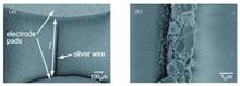
Xiaoyan Sun, Chang Liang, Wei Zhang, Dejian Kong, Yuting Feng, Youwang Hu, and Ji’an Duan
ObjectiveSignificance electronic and information devices are becoming increasingly miniaturized and portable with technological advancements. These advancements require high-density distribution of device function units. This introduces new challenges to the electrical and optical interconnection technology among function units. Some techniques such as photolithography and electron beam have been developed for fabricating microelectrical and micro-optical devices. Although these methods have high resolution, they are inflexible for three-dimensional (3D) fabrication. Ultrafast pulse lasers are a versatile tool for fabricating microelectrical/optical devices owing to their high resolution, minimal thermal effect, and flexibility. In this study, we briefly introduce the basic mechanism of ultrashort pulse lasers for microelectrical/optical interconnection, including multiphoton-induced reduction, surface plasmon resonant, and two-photon photopolymerization. Furthermore, this study focuses on the application of ultrafast laser manufacturing in microelectrical/optical interconnection.ProgressAccording to different applications, femtosecond laser interconnect technology can be categorized into electrical and optical interconnections. Between them, electrical interconnection technology can be used to connect zero-, one-, and two-dimensional nanomaterials.For zero-dimensional nanomaterials, ultrafast laser-induced interconnection mechanisms include multiphoton reduction, photodynamic assembly, and selective laser sintering. Multiphoton reduction is a high-resolution approach for 3D electrical interconnection owing to the multiple absorptions induced in the metal-ion precursor (Fig. 1). To improve the quality of electrical structures, surfactant (Fig. 2) or polymeric matrix (Fig. 3) is added to the precursor to avoid the diffusion of ions. In addition, photodynamic assembly for electrical interconnection is developed to address the diffusion of metal ions in the precursor. This method uses laser-driven force to capture and connect nanoparticles (Fig. 4). Furthermore, selective laser sintering can be used to fabricate patterned electrodes in the atmosphere using surface plasma resonance (Fig. 5).In nanowire electrical interconnection, femtosecond laser-induced local plasma resonance can be used to weld homogeneous nanowires or nanowires and substrate. Studies have shown that local-field enhancement appears at the ends of nanowires or coupled gap regions during femtosecond laser irradiation, inducing localized plasmon resonance to generate localized high temperatures, which can be used for nanowire joining, cutting, or reshaping. For example, silver nanowire networks will have local plasma resonance at junctions during femtosecond laser irradiation, resulting in a localized high temperature, to realize nanowire welding and reduce the sheet resistance of silver nanowire transparent conductive films (Figs. 7 and 8). The welding between heterogeneous material interfaces can also be realized to form electrical interconnection using local plasmon resonance induced via femtosecond lasers, such as Ag-TiO2 nanowire welding and TiO2 nanowire-Au electrode welding (Fig. 12). In two-dimensional material electrical interconnection, femtosecond laser direct writing induced reduction of graphene oxide can be used for electrode repairing or adjustment. To realize one- and two-dimensional material electrical interconnection, femtosecond laser has the advantages of small thermal impact, almost no thermal damage occurs to substrates, and high processing resolution. Therefore, the method of welding nanomaterials using femtosecond laser irradiation has important application prospects in developing flexible electronic devices and functional micro-nano devices.In optical interconnection, femtosecond laser modification processing can often induce refractive index changes in glass and crystalline materials. Two-photon polymerization can be used for additive manufacturing outside the base material, which can process complex 3D structures compared with femtosecond laser modification(Fig. 13). The annealing treatment after modification processing can effectively reduce the transmission loss of a waveguide; beam shaping technology can improve the processing efficiency of the waveguide. However, efforts are still required to improve the compatibility of waveguide manufacturing. Among discrete components, relatively simple couplers, beam splitters, and microlenses have been extensively studied. However, further research is required to fabricate complex devices such as on-chip light source, modulator, and detector component.Conclusion and ProspectElectrical/optical interconnection can be realized via femtosecond laser irradiation primarily through the principles of photon reduction, photodynamic assembly, laser-induced surface plasmon resonance, two-photon polymerization, or material phase transition. The interconnection process is complex, involving photon absorption, energy transfer or transformation, material phase transformation, etc. Laser processing involves the interaction between light, heat and materials. The welding of materials is usually the result of a combination of various mechanisms; therefore, further research is required. In addition, the smallest structure size can reach the submicron level. However, further reducing the characteristic size, reducing resistivity or transmission loss, and improving oxidation resistance and processing efficiency are still the challenges faced by the electrical/optical interconnection. With more understanding of ultrashort pulse laser processing, related technologies will play a more important role in the field of microelectrical/optical interconnection.
May. 01, 2022Vol. 49 Issue 10 1002502 (2022)
Weigao Sun, Lingfei Ji, Jincan Zheng, Yanan Wen, and Guanqiang Wang
ObjectiveLithium niobate crystals with deep microhole structures are excellent photonic-crystal devices with modulation properties of wavelength selection. However, current fabrication methods, such as focused ion beam etching, chemical etching, or conventional laser drilling, remain a considerable challenge for obtaining microholes with high-aspect-ratios in lithium niobate crystals. This paper presents a strategy for the one-step fabrication of uniform deep microhole arrays with a 700∶1 aspect ratio within lithium niobate crystals using the ultrafast laser temporal Bessel shaping technique. This efficient and high-quality strategy for fabricating deep microhole arrays has excellent process stability. The prepared lithium niobate microhole array has remarkable selective beam transmittance, and we hope that this strategy can be used as a promising method for fabricating lithium niobate photonic-crystals.MethodsIn this study, the original femtosecond Gaussian beam was transformed into a zero-order Bessel beam using a series of beam shaping units and the energy distribution of the femtosecond Bessel beam was calculated via COMSOL simulations. The one-step fabrication of deep microholes was realized using the high peak power of the femtosecond laser and by adjusting the spatial energy distribution of the Bessel beam. By matching the pulse frequency and the speed of the moving stage, stable and uniform fabrication of large-area deep microhole arrays could be achieved by varying beam energy and the relative focal position. The resulting microhole morphology and aspect ratio were evaluated using scanning electron microscope, confocal laser scanning microscope, and optical microscope. Additionally, the beam transmission test was performed on the microhole arrays, verifying the structure’s excellent selective beam transmission ability.Results and DiscussionsThe femtosecond Bessel beam obtained after beam shaping successfully realized the fabrication of microhole arrays with a 700∶1 aspect ratio. Varying the laser power can effectively adjust the morphology and aspect ratio of the fabricated microhole. With an increase in laser power, the diameter and depth of the microhole become larger but the aspect ratio gradually decreases. At the same time, an increase in laser power can lead to a side lobe etching effect on the sample surface, resulting in degradation of the device performance or even its damage. Variation in the relative focal position slightly changes the microhole diameter but considerably affects the depth of the microhole. Furthermore, maximum utilization of the Bessel beam energy can be achieved when the Bessel beam is focused at the center of the sample, and a complete through-hole of a 500 μm thick lithium niobate crystal is realized. This high-aspect-ratio microhole array demonstrates excellent selective transmission of light beams in the 450510 nm range.ConclusionsIn this study, a femtosecond Bessel beam is successfully used to rapidly produce a uniform array of microholes with an aspect ratio of 700∶1 inside a lithium niobate crystal. The effects of laser output power and relative focal position on the microhole’s morphology, depth, and aspect ratio are systematically studied and summarized. The laser power range for inhibiting the side lobe etching effect and the design principles of the microhole array are presented. The high-aspect-ratio lithium niobate photonic-crystal filter is fabricated based on the optimization of the processing parameters, and the wavelength-selective transmission of the structure for beams in the range of 450510 nm is demonstrated through the transmission spectrum measurements. The efficient and reliable processing of high-aspect-ratio microhole structures provides a new pathway that is worth exploring for the fabrication of lithium-niobate-based photonic-crystal devices.
May. 01, 2022Vol. 49 Issue 10 1002503 (2022)
Lei Wang, Xu Zhang, Yi Wang, Lin Wang, Qing Wang, Xue Zang, Ruifan Li, Yishi Xu, Zhenze Li, and Qidai Chen
SignificanceNowadays, the using of big data is reshaping our lives via artificial intelligence (AI) and internet of things (IoT) by penetrating education medical care, business, entertainment, and so on. Industrial companies around the world are sparing no effort to collect much data to obtain market conditions, competitors, and logistics information for profits and have long created TB- or even PB-scale information. Meanwhile, consumers are integrating social media, entertainment, and real-time personalized services on mobile devices to connect with friends and shop online. According to the International Data Corporation (IDC), there is an explosive growth in global data, which is estimated to reach 175 zettabytes (ZBs) by 2025. However, the disparity between the amount of digital data and the available storage capacities is enlarging. Most importantly, data storage accounts for 1% of global electricity consumption and exert enormous pressure on resources and environments. However, none of the current medium is capable to meet the requirements. In especial, the cold data storage that is for culture, history, scientific research and these important but infrequently used data is urgently calling for long-term and high capacity medium.Therefore, we are challenged with the arduous task of developing next-generation data storage technologies, where femtosecond laser direct writing for eternal data storage offers a practical solution with low energy consumption, long lifetime, and high capacity. With multiplexing degrees of freedom, this technology’s achievable limit capacity could reach 360 TB/disc. Furthermore, accelerated aging measurements show that nanograting has unprecedentedly high stability, including thermal stability up to 1000 ℃ and a practically unlimited lifetime.ProgressWe reviewed the research progress of femtosecond laser direct writing for eternal data storage. At first, we introduce the interaction between femtosecond laser and materials by reviewing three types of modification. On this basis, the concept and basic physical mechanism of femtosecond laser permanent optical storage were introduced. Then, we reviewed the development of 3D optical storage and 5D optical storage, as well as the structure formation mechanism in detail. Next, we introduced the high-density storage of over 100 layers and fast data recording at a speed of 100 kB/s via a single channel (potential MB/s via multichannel). At the final, based on electronic field continuity conditions at the nanoscale, we calculated the theoretical bottleneck and physical limit of optical storage by femtosecond laser direct writing.Conclusion and ProspectFemtosecond laser direct writing inside hard materials for permanent optical storage provides an unexceptionable solution for cold data storage to meet the demands of big data era. However, there are still some significant scientific and technical problems that must be addressed between the laboratory and the industrial application. For instance, volumes of nanograting must be minimized, and the dot and layer spacing must be reduced to increase the storage density. Moreover, fast writing with fewer pulses and new data readout algorithms for accurate and fast data readout are required. We firmly believe this technology will support every aspect of our lives and bring huge economic benefits to society in the future.
May. 01, 2022Vol. 49 Issue 10 1002504 (2022)
Haoyu Li, Chengjun Zhang, Qing Yang, Xun Hou, and Feng Chen
SignificanceAs the next big trend in the development of the electronic industry, flexible electronics is a brand technology that can revolutionize the future. At present, the application research of flexible electronic devices mainly focuses on human health detection, flexible robot, and human-computer interaction. Flexible electronic devices are realized by combining soft materials and flexible electrode materials to achieve high flexibility. Conventional flexible electrode materials, such as structured metal films, metal nanoparticles/wires, and conductive polymers, cannot meet high stretchability and high conductivity simultaneously. As a new kind of flexible electrode material, gallium-based liquid metal (Ga-LM) with high electrical conductivity and unlimited stretchability has become a research hotspot in recent years. Ga-LM has a melting point below 30 ℃ and the almost negligible vapor pressure. It is non-toxic to the human body and has the excellent conductivity/thermal property, making it an ideal flexible electrode material. Ga-LM based flexible devices are fully flexible compared to traditional electrode materials, which can maintain their electronic performances even under large elastic deformation. This will lead to dramatic improvements in the performance of wearable electronics. The Ga-LM circuits are crucial for the preparation of flexible electronic devices. Although researchers have proposed many methods to prepare the Ga-LM flexible circuits such as screen printing, injection, and spray painting, there still remain problems of limited resolution and integration of Ga-LM circuits. Therefore, to develop a way for the preparation of miniaturized, high-integration, and multifunctional Ga-LM flexible devices is of great interest. Ga-LM patterning is a necessary step in the preparation of Ga-LM based flexible electronic devices. However, there exists a major challenge in Ga-LM patterning due to its fluidity. Hence, the patterning method by tuning the wettability of Ga-LM has been extensively explored in recent years.As a precision machining method, the laser has good processing advantages in preparing various functional surfaces. Due to its high-power density, the laser can induce micro/nano-structures on the surfaces of various materials and realize the preparation of functional surfaces. Ga-LM is found to show extremely high adhesion on the smooth material surfaces, and show ultra-low adhesion on rough surfaces. Selective adhesion of Ga-LM can be realized by constructing rough structures on the initially smooth material surface, so as to realize the printing of Ga-LM circuits. Laser machining technology has advantages of non-contact, high-precision, and high-controllability processing, which can realize the preparation of high-resolution and high-integration LM circuits. The combination of laser manufacturing technology and newly flexible electrode materials can achieve high-performance flexible electronic devices. This field is growing rapidly, and it is necessary to review and analyze all these efforts to guide its future development more rationally.ProgressThe recent efforts in the field of Ga-LM based flexible electronic devices fabricated by a laser are reviewed and the future research directions are indicated. First, this paper introduces the patterning method by tuning the wettability of Ga-LM. The wettability model of Ga-LM is analyzed in-depth (Fig. 2). Then, the characteristics and advantages of laser micromachining are summarized according to previously reported studies. As a precision machining method, the laser is used to prepare various functional surfaces and is one of the main methods to tune the wettability of liquids. Subsequently, recent advances of the Ga-LM-based flexible electronics fabricated by a laser are comprehensively summarized. The research group from the Southern University of Science and Technology has realized the tenability of the wettability of Ga-LM by laser ablation of nanoparticles (Fig. 3). The research group from Xi’an Jiaotong University has reported a method for inducing rough structures directly on the surface of the substrate by a femtosecond laser to change the wettability of Ga-LM on the original smooth surface from the original high adhesion to ultra-low adhesion (Fig. 4). Combining the high precision machining capability of the laser with the excellent electrical properties of Ga-LM, one can fabricate ultra-flexible electronic devices with high-resolution, multi-function, and high-integration. In the end, the applications of Ga-LM based flexible electronics in human health monitoring, human-computer interaction, and soft robots are elaborated.Conclusion and ProspectAs a precision machining tool, the laser has good processing advantages in preparing various functional surfaces. Using a laser to tune the wettability of Ga-LM can realize the preparation of Ga-LM circuits with high resolution and high integration, thus greatly improving the performance of Ga-LM based flexible electronic devices. Ga-LM has intrinsic advantages in the field of flexible sensing, and the improvement of sensor performance is closely related to the preparation of microstructures. Using the advantages of laser precision preparation of microstructures to realize the significant improvement of the performance of Ga-LM sensor will become the key factor to promote the application of Ga-LM in the field of flexible sensing. The combination of laser precision machining with Ga-LM is believed to promote the rapid development of flexible electronics.
May. 01, 2022Vol. 49 Issue 10 1002505 (2022)
Han Liang, Shusen Zhao, Lu Jiang, Chen Zou, Jie Xu, Zhiyan Zhang, and Xuechun Lin
ObjectiveCarbon fiber reinforced plastics (CFRP) are widely used in aerospace, sports, medical, transportation and other fields due to their advantages of high specific strength and high specific modulus. Taking Boeing 787 aircraft as an example, the mass fraction of composites in the aircraft structure has reached more than 50%. Composite structures of the aircraft are vulnerable to be damaged in harsh environments during long-term service, and composite structure repairing is an important part in aviation equipment maintenance. The committed step of composite structure repairing is the damaged zone removal at a small angle, usually 2°6°, which is difficult for mechanical processing. At present, it mainly relies on manual grinding, which shows low efficiency and poor controllability. Laser beam machining (LBM) has the advantages of high precision, high efficiency, and high controllability. It is suitable for difficult-to-machine materials including CFRP, and has excellent performance in laser cutting, drilling, welding, cleaning, etching and other applications. The structural characteristics and thermal-physical properties of CFRP materials result in a more complex physical process for laser removal of CFRP than that for metal materials. The existing studies mainly focus on the thermal process of laser removal of CFRP and the surface state evolution mechanism, but little attention is paid to the thermal-mechanical couple ablation process based on the non-homogeneous characteristics of the CFRP. In this paper, a 1064 nm nanosecond pulsed laser is used for laser removal of CFRP, and the effects of process parameters on removal efficiency, quality as well as the process optimization methods are studied. Based on the anisotropic heat transfer mechanism, the effect of laser scanning angle on material removal rate (MRR) is investigated and the influence of laser spot overlapping rate on thermal-mechanical ablation of CFRP is also discussed.MethodsMultidirectional and unidirectional carbon fiber composite laminates are milled by a 1064 nm nanosecond laser. Fig. 1 shows the laser scanning area and path. The solid line represents the light-on state, and the dashed line represents the light-off state. The variations of ablation depth (h) with power (P), scanning speed (v), hatching distance (d), and scanning angle (θ) are tested, and the variations of the corresponding MRR with process parameters are also calculated. The macroscopic and microscopic morphologies of the sample surfaces are obtained by optical microscope and scanning electron microscope.Results and DiscussionsThe laser peak power density shows a significant effect on the removal quality. Since the transmittance of the epoxy resin matrix in CFRP to the 1064 nm wavelength laser is about 80%, most of the laser penetrates the surface resin and directly acts on the carbon fiber during laser processing of CFRP, causing the carbon fiber to heat up, oxidize, and vaporize. Under the action of heat conduction, the epoxy resin around the carbon fiber is heated, ablated, and vaporized. The surface morphologies under different peak power densities are shown in Fig. 3. Since the axial thermal conductivity of the carbon fiber is about ten times the radial thermal conductivity, the preheating effect is more significant when the scanning direction is along the carbon fiber axial direction which results in a decrease in MRR with the increase of scanning angle (Fig. 4). The scanning speed and hatching distance determine the spot overlapping rate (αA) along the scanning direction and the spot overlapping rate (αB) perpendicular to the scanning path, respectively. As shown in Figs. 7 and 9, at a specific overlapping rate, the MRR peaks, which is caused by the thermal-mechanical ablation effect (Figs. 8 and 10). Multi-layer stepped removal of multi-directional carbon fiber composite laminates is carried out, and it is found that the ablation depth decreases with the increase of defocusing distance (Fig. 13). When the defocusing distance is shorter than the Rayleigh length of the focused beam, the precision of the removal depth is controlled within ±20 μm (Fig. 12).ConclusionsIn this paper, the influences of process parameters such as peak power density, scanning angle, and spot overlapping rate on MRR and removal quality are investigated, and the physical mechanism is disclosed in the removal process of CFRP with a 1064 nm nanosecond pulsed laser. Based on the anisotropic heat transfer mechanism, the influence of laser scanning angle on the material removal rate is studied. The smaller the scanning angle, the more significant the preheating effect, and the larger the ablation depth, 220 μm at 0° and 150 μm at 90°. The physical mechanism of the effect of spot overlapping rate on the thermal-mechanical ablation of non-homogeneous materials is explored, and MRR is improved by using this mechanism. The 18-layer stepped removal of the multi-directional CFRP laminate is carried out, and the precision is controlled within ±20 μm. The influence of laser defocusing state on MRR is discussed. This research provides a process optimization strategy for practical processing applications and improves the processing efficiency and quality.
May. 01, 2022Vol. 49 Issue 10 1002405 (2022)
Research on Parameters Optimization of Diamond Microgrooves Processed by Ultravilot Nanosecond Laser
Xinyu Wei, Qiuling Wen, Jing Lu, Guoqin Huang, Changcai Cui, and Feng Jiang
ObjectiveDiamond has excellent properties such as extremely high hardness, good thermal conductivity, extremely high electron mobility, broadband transparency and high chemical stability, which makes diamond widely used in the fields of microelectronic components, field emitters, high-power semiconductor equipment and cutting tools. High-aspect-ratio diamond microgrooves have more usable area in the vertical dimension, so that they can meet the heat dissipation requirements of high-power microelectronics devices. However, due to the extremely high hardness and chemical stability of diamond, it is difficult to process diamond microstructures with traditional mechanical and chemical methods. As a result, the laser processing and ion beam etching have become mainstream methods for diamond machining. However, ion etching equipment has high cost, low etching efficiency, and requires a vacuum environment, which is not suitable for industrial production. Laser processing has been widely used in diamond processing because of its advantages of high processing efficiency, simple processing technology, low cost and easy automation. In this study, the influences of laser processing parameters such as laser pulse energy, scanning speed, scanning times, repetition frequency and defocus distance on diamond microgrooves are systematically studied. The research results in this paper can provide technical support for the fabrication of high-aspect-ratio diamond microstructures and diamond related devices.MethodsThe experimental material is chemical vapor deposition (CVD) single-crystal diamond. First, a series of microgrooves are directly processed on the surface of CVD diamond plates using an ultraviolet nanosecond laser. Then, a scanning electron microscope is used to observe the surface and internal microscopic morphologies of diamond microgrooves, the width and depth of diamond microgrooves are measured using a three-dimensional video microscope, and the ablation products of ultraviolet nanosecond laser processing of diamond are analyzed using a Raman spectrometer.Results and DiscussionsThe diamond microgrooves processed by ultraviolet nanosecond laser have no cracks and chippings, but a large number of ablation particles with diameters of 200-1000 nm are observed around and within the microgrooves (Fig. 2). Raman spectroscopy shows that the ablation products on the surface of diamond microgrooves are mainly graphite (Fig. 3), indicating that the diamond material removal is through surface graphitization of diamond induced by ultraviolet nanosecond laser. The width, depth, and ratio of depth-to-width of diamond microgrooves increase rapidly with the increase of pulse energy, and then stabilize (Fig. 5). The width(D), depth (H) and ratio of depth-to-width (S)of diamond microgrooves gradually decrease with the increase of laser scanning speed (Fig. 7). As the number of scannings increases, the depths of diamond microgrooves first increase rapidly and then gradually stabilize (Fig. 9). The laser repetition frequency has little effect on the width of diamond microgroove. With the increase of repetition frequency, the H and S of microgroove first increase and then tend to be stable (Fig. 11). The defocus distance also has a great influence on the width, depth and ratio of depth-to-width of the microgrooves processed by ultraviolet nanosecond laser. As the diamond sample moves upward, the defocus distance first decreases and then increases, resulting in the widths of diamond microgrooves first decrease and then increase, and the depths of the microgrooves first increase and then decreases. When the defocus distance is -1 mm, the ratio of depth-to-width of the microgrooves is the largest (Fig. 13). Microgrooves with ratio of depth-to-width of over 12 can be obtained by machining diamond with optimized parameters.ConclusionsIn this study, an ultraviolet nanosecond laser is used to process microgrooves on the diamond surface, and the effects of laser pulse energy, scanning speed, scanning times, repetition frequency and defocus distance on the width, depth and ratio of depth-to-width of diamond microgrooves are studied. With the increases of laser pulse energy and scanning times, the ratio of depth-to-width of the microgrooves increases rapidly and then tends to be saturated as the pulse energy increases to 200 μJ and the number of scannings reaches 30. As the scanning speed increases, the ratio of depth-to-width of the microgrooves gradually decreases. As the laser repetition frequency increases, the ratio of depth-to-width of the microgrooves gradually increases and then tends to be stabilized when the repetition frequency reaches 60 kHz. The ratio of depth-to-width of the microgrooves first increases with the decrease of negative defocus distance and then it decreases with the increase of positive defocus distance. When the negative defocus distance is -1 mm, the ratio of depth-to-width of diamond microgroove is maximum. Therefore, the laser parameters used for processing diamond microgrooves are as follows: the laser pulse energy is 200 μJ, the scanning speed is 5 mm/s, the number of scannings is 30, and the repetition frequency is 60 kHz, the defocus distance is -1 mm. The experimental results show that the ratio of depth-to-width of diamond microgrooves is greater than 12 and the diamond microgrooves have no cracks and chipping using the optimized processing parameters. Raman spectroscopy shows that the ablation products of diamond microgrooves are graphite, indicating that the laser processing of diamond is carried out by surface graphitization. There are obvious graphite residues in the microgrooves because it is difficult to remove the graphite from the bottom of diamond microgrooves with high aspect ratio.
May. 01, 2022Vol. 49 Issue 10 1002406 (2022)
Mingduo Zhang, Chunsan Deng, Xuhao Fan, Zexu Zhang, Ajun Chen, Yufeng Tao, Yuncheng Liu, Binzhang Jiao, Hui Gao, and Wei Xiong
SignificanceIn 1959, Feynman gave a talk titled "There’s Plenty of Room at the Bottom" , in which he addressed the issues of controlling and guiding things in the micro/nano scale, as well as the huge potential of this field. There has been an explosion of continuing and in-depth research on materials, manufacturing, manipulation, and characterization in the micro/nano scale since then. Using the micro/nano technologies, physicists and chemists can view the consequences and even the process of reactions in the microscale, biologists can handle a single cell, and engineers can construct integrated circuits with a resolution of several nanometers. However, static architecture is becoming more and more difficult to meet the future demands of complex environment adaptation and multi-functional integration in the micro/nano domain.4D printing was first proposed by Tibbits at a TED (technology, entertainment, and design) talk in 2013. Although there is no precise definition, 4D printing is often interpreted as "3D printing+ time, " which means that the qualities of a static object (shape, property, etc.) change in response to a specific external stimulus. From the macro-field to the micro/nano field, the reaction time of the micro/nano devices is substantially shortened, the response sensitivity is much enhanced, and the demand for actuation energy is much lowered. In view of the potential of the micro/nano 4D printing technologies as mentioned above, it is necessary to make a review of the recent research progress on the micro/nano 4D printing techniques.ProgressFirst of all, we summarize the commonly used micro/nanofabrication technologies, including direct ink writing, digital light processing, projection micro-stereolithography, and two-photon polymerization (Table 1). Among these various techniques, two-photon polymerization has become the most popular technology in the field of micro/nano 4D printing because of its excellent processing precision of tens of nanometers and true 3D processing ability. Second, we introduce the common material systems in the micro/nano 4D printing field, including intelligent hydrogel, liquid crystal elastomer, shape memory polymer, and biological-based materials (Fig. 2). The mechanisms of the stimuli-responsiveness of four kinds of intelligent materials are introduced. Third, we summarize the recent research in the micro/nano 4D printing field from the perspective of stimulus response. The first is the magnetic response and we summarize the recent works on how magnetic field changes the shape of one body. For example, the magnetic field drives the cilia to swing, which makes the "Paramecium" move. The varying magnetic field drives the complex deformed "bird" (Fig. 3). The solvent response is a direct mode of actuation. The opening and closing of stomata and the opening and closing of flowers are caused by the adsorption/desorption of water in the environment by the polymer (Fig. 4). The pH response is a widely used actuation method. At present, the pH response has been used to achieve certain complex deformation, such as the panda expression change (Fig. 5). The temperature response is also a widely used actuation mode. The temperature response can induce three different mechanisms, including hydrogel phase transition, liquid crystal phase transition, and material thermal expansion deformation. Figure 7 shows the work of the deformation caused by different principles. The light response is a more efficient mode of actuation, which can be precisely controlled by adjusting the power, position and duration time of a laser beam. Pure photothermal response is easiest to achieve (Fig. 8). More complicated motion control can be realized by the photothermal effect combined with the photochemical effect, Marangoni effect and others. Research based on the photoelectric effect has also been reported recently, by which the surface electrochemical effect is excited (Fig. 9). At the end of this section, we summarize the characteristics of the above-mentioned actuation methods (Table 2). Finally, we show some typical applications of 4D printing. In the field of biomedicine, the micro-helix can transport cells in a magnetic field, and the micro-drug-loaded fish can release drugs in a targeted way. In the field of micro-mechanics, the synthetic micro-walker can dynamically respond to the walking behavior of micro-devices, and the micro-gripper can accurately grasp and transport tiny particles. The micro/nano 4D printing technology can also be used in the micro-optical field to achieve focal length tunable diffraction gratings and artificial compound eyes.Conclusions and ProspectsMicro/nano 4D printing is the most advanced manufacturing technology for dynamic response of micro/nano devices, and it is expected to have great applications in many frontier fields such as biomedicine, microelectromechanical systems, flexible electronics, reconfigurable surfaces, and metamaterials. We believe that the future research can make breakthroughs in the following areas: 1) developing more accurate and efficient micro/nano processing methods; 2) developing high performance responsive materials with better response sensitivity, better actuation, and better biocompatibility; 3) developing and optimizing the control methods to achieve more efficient, more accurate individual control, and more intelligent cluster control; 4) enhancing the integration of scientific research with the application scenario. In the future, we believe that the micro/nano 4D printing technology should and must play a greater role in human cognitive exploration of the micro-world and make a greater contribution to improve human life.
May. 01, 2022Vol. 49 Issue 10 1002701 (2022)
Jiaji Cao, Siyu Xiu, Jinkai Xu, and Huadong Yu
SignificanceThe micro-nano structures in nature contain endless functions, which bring new opportunities for the innovation and development of material science and engineering technology. Inspired by biological functional surfaces, many new applications have been developed for biomimetic surfaces, such as structural colors, superhydrophobicity, self-cleaning, and optical performance improvement. Femtosecond laser direct writing technology is a processing method that can accurately control the material structures in the micro-nano scale. By adjusting the femtosecond laser processing parameters, 3D processing beyond the diffraction limit can be realized in a variety of material systems. The unique feature of the femtosecond laser direct writing technology is that it can realize the cross-scale modification of materials, and prepare more complex micro-nano structures through simulation and optimization. In this review, the characteristics and processing advantages of femtosecond laser are first introduced, and then the applications of femtosecond laser in the fields of structural colors, superhydrophobicity, anti-reflection, and bionic compound eyes are described in detail. In addition, the applications of the femtosecond laser fabrication of bionic functional micro-nano structures in other fields are briefly illustrated. Finally, the development of the femtosecond laser fabrication of bionic functional micro-nano structures is prospected.ProgressIn the long and brutal process of natural selection and biological evolution, various organisms have evolved their own unique functions to adapt to the environment. With the help of microscopic imaging, it has been found that the surfaces of many organisms are covered with many micro-nano structures. It is the different characteristics of these micro-nano structures that enable the organisms to adapt to extreme living environments. In line with the principle of learning from nature, researchers have carried out a lot of research on the micro-nano structures of biological surfaces, using different processing methods to imitate the structures of organisms in a variety of material systems, realizing the structural colors of material surfaces, superhydrophobicity, anti-reflection, large field of view angles and other functions. At present, nano-imprint printing, 3D printing, plasma etching, photolithography, ultra-fast laser processing, and other technologies have been used to achieve the preparation of bionic functional micro-nano structures. Among them, the femtosecond laser processing technology has the characteristics of high precision, cold processing, and diffraction limit breaking, and has an obvious technical complementarity with the traditional processing methods. Nature may be said to be the guide to the extreme manufacturing of modern industry. Therefore, the bionic design born from learning from nature presents unique functional characteristics due to the micro-nano structures of their unique surfaces widely used in radar, submarine, aircraft, corrosion resistant coating, and self-cleaning occasions. The femtosecond laser direct writing technology is widely used in the controllable fabrication of bionic micro-nano structures. A femtosecond laser has two obvious characteristics. One is that the duration of a femtosecond laser pulse is very short, which inhibits the formation of thermal action zones around the laser focus area. The other is that a femtosecond laser has a very high peak power, which far exceeds that of the Coulomb field in atoms. This kind of technology is highly accurate, simple, and efficient. Compared with other micro-nano manufacturing technologies, it also has the advantage of good compatibility with materials. Bioinspired micro-nano surfaces have been widely concerned in the industrial field and the academic circles due to their wide application background, such as self-cleaning, oil-water separation, and fog collection. This paper reviews the new progress in the preparation of biomimetic functional micro-nano structures by a femtosecond laser, and shows their properties in structural colors, surface wettability, optical performance regulation, and so on. The potential application prospects of the femtosecond laser preparation of biomimetic functional surfaces in present and future are discussed.Conclusion and ProspectDue to the limitation of the length of this article, other excellent femtosecond laser fabrication of bionic micro-nano functional structures and their applications cannot be introduced in detail. The femtosecond laser direct writing technology can be used to simulate and fabricate the surface micro-nano structures of lotus leaves, nepenthes plants, rice leaves, butterfly wings, and gecko fingerprints. These structures include micro-pores, micro-columns, periodic structures, and self-assembled structures. The microstructures can realize self-cleaning, anti-ice, oil-water separation, bubble manipulation, structure colors, fog collection, underwater bubble collection, droplet transport, shock resistance, adhesion, and other functions. In this paper, the applications of femtosecond laser direct writing to fabricate bionic functional micro-nano structures in structural colors, superhydrophobicity, and optical performance control are reviewed. The biological surface micro-nano structures have provided infinite inspiration for researchers and stimulated a large number of excellent works on the ultra-fast laser fabrication of bionic functional surfaces. However, there are still some problems, such as how to quickly and efficiently simulate complex natural surfaces and how to accurately reproduce cross-scale micro-nano structures. There is no doubt that the solution of these problems will further enhance the competitiveness of the femtosecond laser fabrication of bionic functional micro-nano structures. It is believed that with the improvement of femtosecond laser micro-nano manufacturing capability and the continuous new inspiration brought to us by nature, the bionic multi-functional surfaces should create more application value in biological, medical, environmental protection, and other fields in future. Finally, an example is given to illustrate the new application of the laser micro-nano fabrication of complex high-resolution structures.
May. 01, 2022Vol. 49 Issue 10 1002702 (2022)
Jiang Li, Xiaojun Gao, Zuoli Fu, Wenjun Wang, Xuesong Mei, and Yuxiang Huang
SignificanceCompared with single eyes, the compound eyes of natural insects are characterized by their microimaging, self-cleaning, wide-field-of-view, and high motion detection sensitivity properties due to their micro-nano multiscale structures and curved distribution of small optical units called "ommatidia" . The artificial implementation of such natural imaging systems has important application prospects in cutting-edge fields of robot visual navigation, unmanned driving, and microaircraft systems; therefore, it has recently become a research hotspot. Although several methods have been proposed for fabricating the artificial compound eye, they face challenges due to some limitations. To date, as an advanced manufacturing technology, ultrafast laser has become an ideal tool for fabricating artificial compound eyes with multiscale structures owing to their good flexibility, high fabrication accuracy, and true three-dimensional processing. In addition, the high transient intensity and high ultrafast laser power give the technology a high resolution beyond the optical diffraction limit, which is enough to fabricate various materials, both hard and soft materials. This article reviews the research progress of ultrafast laser processing of various types of artificial compound eyes, including the planar microlens arrays, superhydrophobic compound eye, and wide-field-of-view compound eye. The problems and development trends of the technology in the fabrication of artificial compound eyes are analyzed, thereby providing an effective reference for further research and development of the artificial-compound-eye-based systems.ProgressThis study analyzes the structural characteristics of insect compound eyes and presents the advantages of using insect compound eyes in optical imaging (Fig. 1). Based on these characteristics, various artificial compound eyes were designed and fabricated. Then, the research progress for fabricating three types of artificial compound eyes using an ultrafast laser was reported and the advantages and disadvantages of different methods were analyzed. (1) Planar microlens array: currently, the use of ultrafast laser for fabricating planar distributed microlens array through laser ablation (Figs. 2 and 3) and swelling (Figs. 5 and 6) has gradually increased. For laser ablation, the technology has the advantages of high processing efficiency and filling factor, whereas for swelling, the surface quality of microlenses is relatively high and its size has high controllability. In addition, by controlling the process, various forms of microlenses such as cylindrical, dual-focus or other microlens with irregular surfaces can be fabricated (Fig. 4). (2) Self-cleaning artificial compound eye (Figs. 7-10): in terms of the self-cleaning artificial compound eye, the nonwetting nanostructures could be fabricated at the interval or on the top of microlens arrays. Both the fabricated surfaces endow good self-cleaning property for carefully controlled structures. For the former, the outside droplets are directly in contact with the optical unit and cause pollution problems. For the latter, the fully covered nanostructures easily deteriorate the transmittance of the microlens array if it is over a certain size or has a narrow distribution. In addition, to obtain neatly arranged nanostructures, combining techniques such as imprinting is necessary because the nanostructures induced by the laser are not uniform. (3) Wide-field-of-view artificial compound eye (Figs. 11-14): for programmable direct laser writing, the structures have high fidelity and the artificial compound eye can be fabricated as designed. However, the single-point scanning procedure suffers from low efficiency and the prepared eyes are generally on the micron scale. To improve the fabrication efficiency, a planar microlens array was first fabricated using the laser-based method. Subsequently, using the air- or hydraulic-assisted deformation, the planar distributed microlens array was transformed into a curved architecture. However, during the deformation of a flexible film, the height of the microlenses decreased while the spacing increased, thereby affecting the functional consistency of the imaging unit. Finally, we analyze problems and development trends of the ultrafast laser processing technology in preparing artificial compound eyes to provide necessary references for developing this field.Conclusion and prospectsArtificial compound eye has several intriguing features and has been widely used in various fields. As the fabrication technology of artificial compound eyes continues to develop, ultrafast laser processing stands out because of its high processing resolution and programmable design. Thus, it allows the fabrication of artificial compound eyes with multiscale structures. With the deepening of the research, various artificial compound eyes with different shapes and arrangements have been proposed to achieve different functions and important progress has been made in laser processing technology. This article reviews the research process of three types of artificial compound eyes and comprehensively analyzes the advantages and disadvantages of the laser-based methods for preparing different compound eyes. Although several challenges hinder the fabrication of artificial compound eyes using ultrafast laser and the existing artificial compound eye vision system still has a big gap in terms of optical performance and self-cleaning ability compared with the natural one, we believe these problems will be resolved and with the continuous development of laser technology and ultrafast laser will become a powerful tool for preparing artificial-compound-eye-based vision system.
May. 01, 2022Vol. 49 Issue 10 1002704 (2022)
Qiang Liu, Jian Wang, Pengpeng Sun, Ming Li, Hui Wang, Zhenshuo Yin, Liuquan Wang, and Kunhang Li
ObjectiveAs a new pattern engraving method of chemical milling parts, laser engraving is one of the important processes in chemical milling for aeroengine casing. This technique can effectively improve the precision and the efficiency of chemical milling. Moreover, it is greatly significant in improving the thrust-weight ratio and the manufacturing efficiency of the aeroengine. In the laser engraving process, according to the numerical control (NC) machining program based on the geometric pattern information and the process parameters of chemical milling, the geometric pattern is engraved on the protective adhesive layer by laser ablation under the control of the optical electromechanical cooperative control system. Laser engraving combines laser processing with the NC technology and a digital manufacturing process that has high precision and efficiency, digitization, and flexibility. The method can also be used for primary/secondary engraving on complex surfaces to solve the engraving bottleneck problem of aerospace complex thin-walled structures. The laser engraving research in China is still in its initial stage and mainly focuses on investigating the primary laser engraving process parameters and the engineering application of foreign laser engraving machines. Less research has been conducted on the key technologies and equipment used for the laser engraving of three-dimensional (3D) complex structure parts, and many technical difficulties have not yet been overcome. This work investigates the key technologies of the engraving process parameters, including laser engraving trajectory planning, optical electromechanical collaborative optimization model, and adaptive matching mechanism. The six-axis, five-linkage NC laser engraving machine tool is developed to provide a new solution to the bottleneck problem of engraving in the chemical milling of the complex thin-walled structures of the aerospace.MethodsFirst, based on the laser multiple engraving process, a laser engraving trajectory planning algorithm considering the chemical milling evolution is proposed herein to solve the laser engraving problem of the complex surface on aeroengine casing. The basic processes of trajectory planning and automatic programming of the pattern features for multiple laser engraving are given. The multi-axis motion trajectory of the laser engraving position and direction is fitted by a complete B-spline curve and a segmented double B-spline curve. The number of control points and the fitting error of the curve are then analyzed. Second, an opto-mechatronics collaborative optimization model is established aiming at the minimum processing time and the minimum width of the heat-affected zone while the adhesive layer is etched through. In this model, the bow height error of the trajectory curve, speed, acceleration, and jerk of the feed axis are considered. Furthermore, the minimum processing time is equivalent to the maximum feed speed. Third, an adaptive matching optimization algorithm for the engraving process parameters is established to solve the optimization problem of the motion and laser process parameters. The laser process parameters that satisfy the constraints under different speed conditions are simulated and calculated, providing theoretical parameters for the optical electromechanical cooperative control of laser engraving. Finally, the structure of the six-axis, five-linkage NC laser engraving machine tool, the high-precision optical path flexible transmission and positioning, and the optical electromechanical cooperative control system are implemented. The six-axis, five-linkage NC laser engraving machine tool is developed to realize the application of primary/secondary laser engraving.Results and DiscussionsFirst, for the trajectory planning of the laser engraving position points, a complete B-spline curve and a segmented B-spline curve are used to generate the trajectory that meets the accuracy requirements. The fitting accuracy of each curve is less than 0.008 mm (Fig. 5). To ensure the fitting accuracy, the complete B-spline curve needs more control points, while the segmented B-spline curve needs less control points (Table 1). The segmented double B-spline curve is used to generate the trajectory for the engraving position and direction. The fitting accuracy of the segmented double B-spline curve of the laser engraving position and direction can reach 0.005 mm (Fig. 5). The maximum error of the direction vector angle by the segmented double B-spline curve is 0.0061 rad, which effectively meets the laser engraving process requirements. Second, the simulation results of the opto-mechatronics collaborative optimization model illustrate that the energy in the heat-affected zone exceeding the threshold is mainly considered in the low-speed movement section. In addition, the engraving speed is increased to ensure the engraving quality (Fig. 8). The kinematic constraints of the equipment are mainly considered to complete the engraving processing with the highest efficiency in the high-speed movement section. The comprehensive balance between the engraving quality and efficiency is realized in this model. Third, to optimize the motion and process parameters in the engraving process, the comprehensive optimization results under different weight conditions are given, and the corresponding process parameters of the laser energy density and the duty ratio under different speeds are calculated (Fig. 9). Different laser motion and laser parameters can be quickly selected through different weight settings. Fourth, the primary engraving/secondary engraving of the annular thin-walled milling cylinder parts of an aeroengine casing is realized. The accuracy error of the secondary laser engraving can reach 0.034 mm, meeting the process requirements of the secondary laser engraving accuracy that should be less than 0.05 mm.ConclusionsThis study investigates the key technologies of the laser engraving process, including laser engraving feature trajectory planning and automatic programming, collaborative optimization control of the laser engraving process, high-precision optical path flexible transmission and positioning, and optical electromechanical collaborative control system. The principle and engineering prototypes of the six-axis, five-linkage NC laser engraving machine tool are successfully developed, consequently providing the key technologies and the equipment support for solving the laser engraving problem of aerospace chemical milling structural parts. The key technologies of the laser engraving process and the six-axis, five-linkage NC laser engraving machine tool will not only solve the manufacturing problem of aerospace chemical milling parts, they can also be widely used in the fine manufacturing of 3D complex surfaces, which will effectively improve the performance and the manufacturing efficiency of major instruments and equipment.
May. 01, 2022Vol. 49 Issue 10 1002401 (2022)
Ting Huang, Weizhe Du, Kun Su, Jianchao Zhang, Jingyang Li, Junfeng Qi, Yongping Lei, Qiang Wu, and Rongshi Xiao
ObjectiveDeep-space exploration is important to innovate space technology and explore space resources. A collimator is a key component of a deep-space probe; however, producing a high spatial resolution collimator is challenging. Currently, the deep-space exploration collimator grid is mostly composed of frames. Casting or laser additive manufacturing is used to build the inner grid structure, which is quite thick, as well as the entire outside wall. The grid frame is then used to create the microgrooves. Finally, the collimator grid is formed by inserting tungsten or tantalum foils into the microgrooves. Furthermore, collimator grid manufacturing technologies include LIGA and electrical discharge wire-cutting. These approaches may result in thick walls, limiting the collimator’s duty ratio and efficiency, or result in a longer manufacturing period, higher cost, and a smaller grid height. The hard X-ray modulation telescope satellite (HXMT), which China developed independently, is used as an example to present our research progress on laser microwelding technology and equipment development for the cross-scale collimator grid, which is funded by the National Key Research and Development Program.MethodsThe laser spot welding experiment was conducted first to identify the welding parameters based on the structural features of the HXMT collimator. The grid deformation finite element analysis was then performed to provide laser welding guidance. Finally, laser welding equipment was designed and validated to meet the grid cell laser welding requirements.Results and DiscussionsThe HXMT collimator is composed of an aluminum alloy frame with many tantalum grid cells placed into it. Laser spot welding junction points formed by two orthogonal arrays of tantalum foils are used to create the grid cell. The fabrication of tantalum foils, grid cell assembly and welding, and grid cell insertion into the collimator frame are all part of the manufacturing process (Fig. 3). For laser welding grid cells, an IPG YLM-150/1500-QCW quasicontinuous fiber laser and a self-developed three-dimensional (3D) dynamic focusing galvanometer are employed. With a beam diameter of 40 μm, laser power of 180-220 W, and pulse width of 6-10 ms, a well-formed welding spot is created (Fig. 4). The results of the finite element analysis show that instability deformation is common during the laser welding of the collimator grid cell (Fig. 5). To address this issue, an integrated set combining tantalum foil assembly and collimator grid welding/insertion is developed (Fig. 6). The assembly error and welding deformation are well-controlled, resulting in the collimating hole’s dimensions accuracy being within ±20 μm. The self-designed laser microwelding equipment consists primarily of a quasicontinuous fiber laser, a self-developed 3D dynamic focusing galvanometer, an X/Y motion platform with a Z support frame and motion axis, a CCD vision inspection system, and a computer control system, among other components (Fig. 7). Before welding, the stage moves to the CCD field of view to locate the welding point; next, the stage moves to the galvanometer, which can quickly and accurately regulate the movement of the laser beam, allowing for the rapid and precise welding of each grid cell’s welding spot. After welding, the stage returns to the CCD field of view to detect and evaluate welding quality (Fig. 8).ConclusionsHigh-efficiency laser microwelding and detection of large depth and high spatial resolution collimator grid have been realized using linkage technology of online visual inspection, dynamic focusing galvanometer, and CNC machine as well as the development of an integrated set to combine tantalum foil assembly and collimator grid welding/insertion, as along with the development of laser microwelding equipment and welding process. The accuracy of collimating hole size can be controlled within ±20 μm for the tantalum collimator grid with 70 μm wall thickness, 1.17 mm×4.68 mm collimating hole size, and 67 mm depth.
May. 01, 2022Vol. 49 Issue 10 1002402 (2022)
Wanqin Zhao, Xuesong Mei, and Zixuan Yang
SignificanceCeramics substrates, Al2O3 and AlN, are commonly used as electronic packaging substrate materials, have many advantages such as small dielectric coefficient, small thermal expansion coefficient, high thermal conductivity, good insulation performance, and good corrosion resistance. In short, ceramics substrates can meet all the performance requirements of microelectronic device packaging and are widely used in the fields of aerospace and military engineering. However, due to the hard and brittle characteristics of ceramics materials, the traditional machining method is easy to cause damage to this kind of materials. Laser processing is an advanced processing technology with no contact processing, no tool wear, high precision, and high flexibility. It is the preferred method for hard and brittle materials processing. At present, there are many researches on the effect of characteristic dimension of laser ablated holes, but the study on the characteristic morphology of laser drilled holes is often ignored. Moreover, when a high energy laser is focused on the material, the strong thermal effect cannot be avoided, which leads to the recast layers, micro-cracks, and heat affected zones on the surface of the ceramics substrate, influencing the morphology of the holes and subsequently influencing the performance of the ceramics substrate. It must be pointed out that the thermal effect has a high correlation with the laser pulse duration. Specifically, the thermal effect of the long pulse laser represented by the millisecond laser is the most serious, and the holes ablated by them have serious spatters, recast layers and micro-cracks. The thermal effect of a short pulse laser represented by the nanosecond laser is relatively small, and the morphological quality of holes is improved greatly. The ultrafast laser (generally referred to the pulse duration ≤12 ps) has the characteristics of "cold ablating" , which can limit the influence of the thermal effect to the maximum, and thus can be used to process the holes with a high morphological quality. In this paper, the morphological characteristics of holes in the electronic ceramics substrate ablated by a millisecond long pulse, a nanosecond short pulse, and an ultrafast laser pulse are reviewed.ProgressAs for the hole circularity, it becomes worse when the scanning speed increases during the millisecond laser processing. During the nanosecond laser processing, the higher the repetition rate, the better the hole circularity. During the ultrafast laser processing, the circularity and machining efficiency can be ensured by selecting appropriate interpolation errors. For the spatters on the holes surfaces, the higher the laser energy, the higher the repetition rate, the wider the spattering range. During the millisecond laser processing, the larger the pulse duration, the more the surface spatters, the wider the spatters range. During the ultrafast laser processing, the faster the scanning speed, the wider the spattering range. The surface cracks of holes induced by laser ablating on the ceramics substrate are mainly caused by the surface stress concentration coming from the thermal effect. The radial cracks are generally induced by the tangential stress, and the ring cracks are by the radial stress. The cracks propagate to form the propagation path of the group hole cracks, which maybe cause the sample to fracture finally. The laser compound machining assisted by water and other liquids, the spatters and cracks on hole surfaces can be reduced and the surface morphologies of holes can be improved.The laser processed hole taper on ceramics substrate is related to laser energy, repetition rate, pulse duration, focus position, air pressure, and processing environment. The faster the scanning speed, the larger the hole taper. During the nanosecond laser processing, the wider the scanning filling circle’s interval, the larger the hole taper. For different hole diameters and depths, a smaller hole taper can be obtained by choosing the appropriate processing filling style. For the recast layer on the hole sidewall, even using an ultrafast laser with the "cold working" characteristics, it cannot be completely avoided. The hole recast layer processed by the millisecond laser is thicker. Under the optimized parameters, the thicknesses of the recast layer processed by the nanosecond and ultrafast lasers are almost the same. Furthermore, the thicknesses of the recast layer can be reduced effectively by the water jet assisted machining and the water environment assisted machining, and it can be completely removed by a post-treatment such as solution corrosion. It should also be pointed out that a large number of microcracks extending along the grain direction are generally distributed on the surface of the recast layer, especially for the millisecond laser processing.Conclusion and ProspectHigh quality holes have been required on the surface of a hard-brittle electronic ceramic substrate processed by a laser in order to achieve high quality and high density interconnection of electronic devices. Morphological features of holes drilled by a long pulse duration millisecond laser, a short pulse duration nanosecond laser and an ultrafast laser are reviewed, mainly including the hole surface morphological characteristics such as hole circularity, spatters, micro-cracks, and heat affected zones on the hole surfaces, and the hole side-wall morphological characteristics such as hole taper, recast layers and micro-cracks on the side-wall surface.
May. 01, 2022Vol. 49 Issue 10 1002403 (2022)
Shuiwang Wang, Ye Ding, Bai Cheng, Yuan Li, and Lijun Yang
SignificanceWith the rapid development of the national aviation, aerospace, communications, instrumentation, and medical fields, components such as fuel nozzles, solar silicon light panels, semiconductor chips, and heart stents tend to be miniaturized and sophisticated. The quality requirements for structures, such as holes and grooves processed on related materials are increasing, which correspondingly translates into higher processing technology requirements. At present, scholars have developed a variety of processing methods, including but not limited to mechanical machining, electrical discharge machining (EDM), electrochemical processing, and laser processing. During the mechanical machining process, the tool is in direct contact with the workpieces, resulting in significant stress. EDM is suitable for conductive materials. There is no obvious force during the machining process, but the machining efficiency is generally slow. Electrode loss exits, and the corner radius is limited. The electrochemical processing efficiency is relatively high, and cathode loss is absent. But the processing stability is poor, and the electrolysis product easily results in environmental pollution. Compared with the above processing methods, laser processing has obvious advantages. It has been widely used for drilling, grooving, and cutting operations in the aerospace, microelectronics, precision medical, instrumentation, and other industries. The continuous laser and the long-pulse laser have high processing efficiency. The continuous laser and the long-pulse laser have high processing efficiency. However, the generation of heat-affected zones and recast layers cannot be ignored. To achieve the eruption and removal of the material, the ultrashort pulse laser directly converts the material into a plasma state. The ultrashort pulse can theoretically achieve the effect of "cold processing" but the processing efficiency is low. Nanosecond-level short pulse lasers have lower acquisition costs and a higher material removal rate than ultrashort pulse lasers, but obvious defects such as heat-affected zones, recast layers, and micro-cracks still cannot be avoided. To overcome the thermal defects in the "dry laser" process, domestic and foreign researchers attempt to develop a composite system that combines laser and water. Compared with "dry laser" processing, water-jet guided laser (WJGL) has many advantages—large working distance; no obvious cone, neat cut, and no burrs; small heat-affected zone; almost no thermal deformation and thermal damage; and high processing quality. This work has provided a relatively complete overview of water-jet guided laser processing technology, allowing us to deeply understand the mechanism of water-jet guided laser processing technology, exert its processing advantages, and broaden its application fields.ProgressThe work first analyzes the water beam fiber’s formation mechanism, including the formation of a stable water jet, the influence of the nozzle on the water jet, and the water jet’s attenuation and divergence process. Then the influence of the coaxial gas on the stability of the water jet and the situation after the jet hits the surface of the workpiece are analyzed. This work systematically elaborates on the optical properties of water and the conditions of total reflection formation to interpret the coupling process of the laser and the water jet. The factors affecting the coupled energy beam’s stability, as well as the influence of the coupling error on energy distribution and jet stability, are explained. The status of water-jet guided laser applications in aerospace, semiconductor, medical, and other fields is reviewed. Based on the summary of the shortcomings of the current technology and the emergence of new requirements and challenges, the future development trend of water-jet guided laser processing technology has prospected.Conclusion and prospectThis work reviews a series of literature on water-jet guided laser and systematically expounds on its formation mechanism and its application potential.1) The formation of water jets is discussed. The "cone-down" nozzle makes it easy to form a stable "retracted flow" water jet. Factors, such as environment and nozzle geometry, are related to the breakage of the water jet. The introduction of an auxiliary atmosphere can increase the stable length of the jet, and the jet will form a liquid film after impacting the processing surface.2) The coupling process of the laser and water jet is discussed. The linear absorption of laser by water is an important factor in energy loss, and the laser energy exceeding the threshold causes stimulated Raman scattering. The laser transmission in the jet can be divided into two types: meridian transmission and oblique ray transmission. The coupling error determines the coupling efficiency and energy distribution, and together with the loss of energy, affects the stability of the coupled energy beam transmission.3) The excellent performance enables water-jet guided laser to be used in aerospace, chip manufacturing, precision medicine, and other fields to process various difficult-to-process materials such as metals, semiconductors, and composite materials. Modeling and simulation provide appropriate help for understanding the physical mechanisms involved in laser ablation and promote the conduct of related experiments and the extension of the application range of water-jet guided laser.A large number of studies on water-jet guided laser have strongly proved its application value. However, the processing capabilities of water-jet guided laser are still limited under processing conditions such as high-quality processing requirements and small working spaces. At the same time, the processing technology for difficult-to-process materials such as diamonds, sapphire, and super-hard ceramics still needs to be further explored. To meet these requirements, the possible research directions of water-jet guided laser in the future are as follows:1) Reduce water jet diameter and transmission energy loss of high-intensity input laser.2) Research on the law of focus movement due to the thermal interaction between the laser and water during the coupling process.3) A thorough examination of the interaction principle between laser, water jet, and material during water-jet guided laser processing.4) Research on the law between the energy distribution of the laser on the machined surface and the evolution of the surface topography.
May. 01, 2022Vol. 49 Issue 10 1002404 (2022)
Yimeng Wang, and Yingchun Guan
SignificanceDue to population aging and change in the modern lifestyle, tens of thousands of people are troubled by orthopedic, oral, and facial diseases. The demand for high-quality medical devices and implants in clinical medicine is increasing. Compared with traditional inorganic nonmetallic and polymer materials, metal materials have better biomechanical properties and processing ability. The surface state of medical devices and implants is an important factor in therapeutic schedules since it affects the complex biological behavior of nearby tissues, such as cell proliferation and differentiation, bone integration, immune response, neurotransmitter release and transport, bacterial infection, and so on. To promote innovation and development in the medical field, it is imperative to develop a simple, efficient, practical, and reliable preparation method for high-performance biological functional surfaces of typical medical devices and clinical implants.Recently, many methods for modifying surfaces of medical metal materials have been developed. Various research methods focus on regulating the corrosion resistance and degradation rate of implants, blocking the release of harmful elements, promoting the adaptation of mechanical properties between implants and biological tissues, increasing biocompatibility, and obtaining antibacterial surfaces. Common surface modification methods include anodic oxidation, micro-arc oxidation, plasma spraying, ion implantation, electrochemical deposition, sol-gel, friction stir treatment, etc.Laser surface modification controls the accuracy characteristics of the implanted surface with high efficiency, no pollution, and low material consumption. It is widely applied to preparing periodic micro/nanostructures on the surface of several materials, providing a new idea for the surface modification of metal materials. Unlike the thermal effect caused by molecular vibration induced by a long-wavelength laser, the femtosecond laser has a very low pulse width. Low pulse energy can obtain high peak power, trigger multiphoton absorption and achieve material removal. The thermal effect in femtosecond laser processing can be ignored and the spatial selective manipulation of microstructure can be realized. Femtosecond lasers are suitable for quasi three-dimensional machining of all materials with high machining resolution. Femtosecond lasers are widely used in the preparation of biological functional surfaces.ProgressBody fluid detection provides an early specific indicator for assessing the health status. It requires stable detection method, high sensitivity, and reproducibility. Researchers have prepared femtosecond laser-induced periodic micro-nanostructures on the surface of titanium alloy. Surface-enhanced Raman scattering (SERS) and surface-enhanced fluorescence (SEF) detection substrates (Figs. 6 and 8) were used for glucose detection and in vitro spectral monitoring of protein. The spectral peak intensity has good linearity with the ion concentration to be detected, and the limit of detection (LOD) concentration and sensitivity is good. Thus, the SERS-SEF double enhancement substrate was prepared using the femtosecond laser for urine glucose detection (Fig. 9). The Raman and fluorescence enhancement factors were 7.85×10⁵ and 14.32, respectively, and the LOD was 14.4 mol/L. Additionally, titanium alloy detection substrate was prepared using femtosecond laser-induced surface periodic micro/nanostructure, providing a new idea for body fluid spectral selection and multitarget recognition and detection.The surface morphology of materials is an important factor affecting the cell behavior on the surface of implants. It is directly related to the subsequent cell proliferation and osteogenic differentiation and is essential in the success or failure of the implant quality scheme. In the study of femtosecond laser-induced surface microstructure regulating the surface cell behavior of clinical implants, laser-induced periodic surface structure (LIPSS), nanopillars (NPs), microgroove, and micropore structure were studied more, among which LIPSS performs well. Femtosecond laser-induced LIPSS is conducive to cell adhesion and serves as a signal to regulate cell migration in a specific direction and stimulate cell proliferation and differentiation (Figs. 11 and 13). One-top femtosecond laser direct writing layered or composite periodic micro/nanostructure of degradable magnesium alloy realizes the increase of cell adhesion on the surface of degradable magnesium alloy, induces cell anisotropic migration and promotes osteoblast bone integration, which provides a new scheme for the clinical application of degradable magnesium alloy.Presently, the mechanism of microstructure realizing antibacterial function is that the contact/suspension interaction between bacteria and microstructure leads to cell body rupture (Fig. 15) and surface superhydrophobic inhibition of bacterial biofilm formation (Fig. 16). The femtosecond laser induced micro/nanostructured on the surface of titanium alloy not only realized the inhibition of bacteria, such as E.coli, S.aureus, P.gingivalis, which are common in the oral clinic, but also obtained the selective inhibition of colonies (Fig. 18). Furthermore, its surface is nontoxic to cells, which provides an effective method to avoid implant infection and inflammation.Conclusion and ProspectPresently, due to the lack of clear biomedical theoretical guidance in the early design of femtosecond laser surface micro/nanostructure technology, the functional effectiveness of micro/nanostructure depends on subsequent experimental verification. Additionally, the simulation and verification environment of the micro/nanostructure function surfaces is relatively single, such as for single-cell/bacterial behavior, signal transmission, and interaction between multiple cells/bacteria, monitoring and regulation of cell/bacterial behavior on a long time scale need to be further studied.
May. 01, 2022Vol. 49 Issue 10 1002601 (2022)
Meiyun Zhao, Fan Yang, Xiaolong Zhang, Yunhui Yin, Yan Zhao, and Xinze Zhao
ObjectiveSilicon rubber composite insulators have been widely used in high-voltage transmission, distribution lines, and some high-voltage transmission parts machinery due to their good electrical insulation, excellent antipollution characteristics, and low maintenance cost. Transmission lines often work in cold and heavily polluted conditions, and the anti-icing ability of insulators affects the safety of transmission lines. As a new anti-icing method, the superhydrophobic surface has the advantages of low energy consumption, light weight, and simple structure. It also shows a good application prospect in reducing ice-covered flashover, fouling flashover, and tower collapse accidents of high-voltage transmission lines. Many domestic and foreign researchers determined that the superhydrophobic surface has a great positive effect in reducing the adhesion strength of ice on the material surface and has a certain effect of delaying icing. The most widely used method for preparing superhydrophobic silicone rubber surfaces is the coating method due to the physical and chemical properties of silicone rubber. However, the coating in harsh environments can easily fail because of the poor mechanical stability and impact resistance of the coating. In previous studies, superhydrophobic surfaces were obtained using chemical reagents to reduce surface energy after laser processing of micro-nano structures. Herein, the silicone rubber composite insulators umbrella skirt material has the characteristics of low surface energy; thus, it requires no modification through chemical reagents. The laser engraving machine is used to process micron-scale texture to obtain a superhydrophobic surface, which has a higher processing efficiency than a nanoscale machine. Therefore, using a laser engraving machine to prepare a superhydrophobic surface to shorten the icing of the silicone rubber composite insulator has a certain application prospect.MethodsHerein, the D80M multifunctional laser engraving machine is used to process different types and dimensional parameter textures on the surface of the composite insulator silicone rubber samples. The surface morphology of the specimens is observed by a three-dimensional morphometer and scanning electron microscope, and the hydrophobicity principles of the specimens are analyzed. The contact angle of the samples with different complex texture surfaces is tested using a contact angle measuring instrument. Consequently, the optimal type and size parameters of complex texture with the best hydrophobicity are obtained. The freezing time of water droplets on the specimen surface is evaluated using a high and low temperature-humidity test chamber to test the freezing time of water droplets on different texture specimen surfaces at -10 ℃. The ice adhesion force on different texture surfaces is also investigated. Furthermore, the anti-icing durability of the specimens is examined by testing the change contact angle and freezing time after repeated icing and de-icing of the specimens.Results and DiscussionsThe textured surface of the specimens prepared by laser processing, without any chemical modification, has good hydrophobicity, and the contact angle of the square + circular texture (Sq+ Ci) surface with the size of 350 μm can reach 154.1° to realize superhydrophobicity (Fig. 4). The study on the anti-icing property shows that the freezing time of the droplet on different complex texture surfaces first increases and then decreases as the size increases. The longest freezing time is reached at the Sq+ Ci texture surface with the size of 350 μm, which is 144 s (Fig. 5). Compared to the original surface with an icing adhesion force of 4.54 N and a freezing time of 72 s, the adhesion forces of the droplet on the three textured surfaces with the optimal size are below 2 N in the same low-temperature condition (Fig. 7). When the environmental temperature change from -4 to -12 ℃, the freezing time of the droplet on the Sq+ Ci texture surface decreases from 355 to 129 s and becomes shorter by about two-thirds, demonstrating that the anti-icing performance of the specimens decreases sharply as the environmental temperature decreases (Fig. 9). Additionally, after 20 times of icing and de-icing, the freezing time of the droplet on the sample surface remains higher than 133 s, indicating that the surface of the silicone rubber processed by laser engraving has good anti-icing durability (Fig. 10).ConclusionsIn this study, the hydrophobicity of silicone rubber can be significantly improved by constructing rough complex microtextures on the surface via laser engraving. The hydrophobicity of the three different complex textures first increases and then decreases as the size increases, and the Sq+ Ci texture with the size of 350 μm has the best hydrophobicity and ice resistance. There is a linear relationship between hydrophobicity and anti-icing performance of different textures. The better the hydrophobicity of the textured surface, the longer the freezing time and better icing resistance due to the slower heat exchange. The surface wear resistance of the textured sample is good. After icing and de-icing, the ice resistance does not decrease too much, and the surface icing can still be delayed to a great extent. After the laser engraving, the textured surface wear resistance of the silicone rubber composite insulator is good, which can be seen from the change in the contact angle and freezing time after multiple icing and de-icing. The textured surface can still delay the surface icing to a large extent. This study has a certain reference value for the design of improving the anti-icing ability of equipment surfaces and provides new ideas for high-efficiency laser processing.
May. 01, 2022Vol. 49 Issue 10 1002603 (2022)
Yansheng Yao, Rui Chen, Zhangsen Ge, Yachao Zhang, Nianwei Dai, and Dong Wu
ObjectiveIn recent years, with the increasing aging of the social population and the rapid increase in the number of orthopedic patients, researchers have developed many orthopedic medical implants. Zirconium-based amorphous alloy is regarded as a new potential material in medical orthopedic implant surgery for its non-degradability and high corrosion resistance and wear resistance. Since the zirconium-based amorphous alloy is a non-biological material, it requires surface-active treatment before surgery when it is used as a medical implant. We can prepare hydroxyapatite (HA) coating on the surface of the implant to improve its biological activity. Studies have shown that the surface of human bone is covered by microgrooves with a width of 10-100 μm and finer nanostructures (such as grooves with a width and depth of several hundred nanometers, pits, and nanoparticles, etc.). Therefore, the researchers use the surface modification technique to prepare similar micro-nano structures on the implant surface to provide a suitable external environment for HA deposition. Traditional surface processing techniques such as machining, sandblasting, and acid etching have been widely used in common metal implant materials. However, when the techniques are used to process the material surface, they have great randomness and low accuracy, making it impossible to accurately prepare the expected micro-nano structure. Because of its non-contact processing and energy-controllable merits, laser surface processing technology can overcome these problems, and it has been widely used to prepare micro-nano structures such as grooves and pores on the surface of metal materials.MethodsIn this paper, a nanosecond laser and femtosecond laser composite processing method for efficiently processing micro-nano structures on the surface of metal implants is proposed. The micro-nano structures of the natural bone surface are prepared on the Zr55Cu30Ni5Al10 surface through laser composite processing technology. A short pulse nanosecond laser is used to fabricate microgroove structures with a width of tens of micrometers on the material surface, which can provide more room for the deposition of HA on the surface of the implant. The finer nanostructures are then prepared using acid etching and ultra-short pulse femtosecond laser processing, respectively. The finer nanostructures can accelerate the agglomeration of HA crystal nuclei and enhance the deposition speed of HA. The experiments are divided into four groups: unprocessed samples, nanosecond laser processed samples, nanosecond laser and acid etching treated samples, and nanosecond and femtosecond laser processed samples. To compare wetting properties, the surface contact angles of samples treated with different surface modification methods are measured. Different samples are immersed in simulated body fluid to deposit HA on the surface, and their deposition speed and mass of HA are compared.Results and DiscussionsThe morphology and water contact angle of the sample surface under different processing methods are shown in Fig.3. The water contact angle of an unprocessed sample is 62°. When the scanning time, scanning speed, laser pulse energy, pulse width, and repetition frequency of a nanosecond laser are 1, 100 mm/s, 0.12 mJ, 10 ns, and 150 kHz, respectively, the width and depth of the fabricated microgroove structure meet the requirements, and the contact angle is reduced to 53°. The water contact angle between the nanosecond laser and the acid-etched sample is 47°. When the scanning time, scanning speed, laser power, and repetition frequency of a femtosecond laser are 5, 20 mm/s, 100 mW, and 1 kHZ, respectively, the water contact angle is 26°. We can find that the hydrophilicity of the sample processed by the nanosecond laser and femtosecond laser is greatly improved. Four different samples are immersed in simulated body fluids, dried, and weighed every 3 days. Measurement of the mass growth of the different samples is shown in Fig. 4. We can find that samples processed by the nanosecond and femtosecond laser have the highest mass growth of HA throughout the soaking period. The distribution of the Ca elements can characterize the distribution of HA on the sample surface. Figure 5 shows the surface morphology of different samples and the distribution of Ca elements on the sample surface. We can find that the Ca element on the surface of the sample processed by the nanosecond laser and femtosecond laser is distributed uniformly.ConclusionsA method of nanosecond laser and femtosecond laser composite processing of zirconium-based amorphous alloy is proposed in this paper. The wettability and HA deposition characteristics of Zr55Cu30Ni5Al10 samples treated by different surface modification methods are studied. Compared with the results of these four groups of experiments, the processing effect of the nanosecond and femtosecond laser composite processing methods is the most excellent. Since the Zr55Cu30Ni5Al10 is intrinsically hydrophilic, in the conditions of nanosecond and femtosecond laser composite processing, the roughness of the sample surface increases, and the hydrophilicity increases accordingly. The composite processing method of the nanosecond laser and femtosecond laser not only improves the hydrophilicity of the Zr55Cu30Ni5Al10 surface but also greatly promotes the deposition speed and mass of HA on the surface.
May. 01, 2022Vol. 49 Issue 10 1002604 (2022)
Yuanyuan Zhao, Haichao Luo, Zixin Liang, Mingjie Deng, and Xuanming Duan
SignificanceAs a micro-nano additive manufacturing (AM) technology, micro-nano 3D printing based on photopolymerization has significant advantages in the manufacture of high-precision and complex micro-nanostructures. Traditional AM technology is essential in printing macroscale structures. However, its printing accuracy is limited, and the difficulty of meeting the demanding requirements for printing accuracy in many micro-nano manufacturing fields has grown tremendously. For example, the printing accuracy of microfluidic chips in the biological field is on a microscale. In micro-nano optics, the period of photonic crystals requires printing accuracy to reach hundreds of nanometers. Additionally, 3D printing technology can manufacture high-precision and complex three-dimensional structures and has huge industrial application needs in micro-nano electromechanical systems, micro-nano photonic devices, micro-fluidic devices, biomedicine and tissue engineering, and new materials. Thus, research on micro-nano 3D printing technology has received widespread attention.ProgressRecently, researchers have developed various types of micro-nano 3D printing technologies suitable for several materials (organic polymers, metals, glass, ceramics, biological materials, composite materials, etc.). Micro-stereolithography (single-photon absorption) and two-photon polymerization using photopolymerization are the most representative micro-nano-scale 3D printing technologies. Micro-nano 3D printing technology based on photopolymerization uses the continuous, pulsed laser or LED light as its energy source. The photopolymerization reaction process is controlled at the micro-nano scale to print and manufacture the micro-nano 3D structure. First, the optical micro-nano resolution of 3D printing mainly depends on the diffraction limit of the optical system, such as the Rayleigh criterion 0.61 λ/NA, where λ and NA are the wavelength of the light source and numerical aperture of the imaging system, respectively. Sub-micron resolution can be obtained using a light source with a shorter wavelength, such as the UV beam, and an objective lens with a higher NA. Additionally, the lithography resolution, which is far beyond the optical diffraction limit (below 100 nm) can be achieved using ultra-fast femtosecond pulse lasers to excite the nonlinear response of the material, such as two-photon or multiphoton absorption effect. Finally, most of the micro-nano 3D printing optical systems are sets of micro-imaging systems, and the lithography resolution is improved using the latest and frontier super-resolution micro-imaging technology. For example, by introducing super-resolution microscopy, stimulated emission depletion (STED), two-color non-degenerate two-photon absorption (ND-TPA), and other technologies, the lithography resolution can be increased to less than 10 nm.Currently, micro-nano 3D printing is one of the most frontier advanced manufacturing fields in the world. In 2014, micro-nano 3D printing was listed in the top 10 disruptive innovations of the year by the Massachusetts Institute of Technology MIT Technology Review. With the rapid improvement of prototyping technology for printing accuracy, efficiency, and other performance requirements, plane projection 3D printing has developed rapidly recently. Compared with traditional micro stereolithography, plane projection 3D printing has advantages including accuracy, efficiency, and equipment cost-efficiency. In 2015, researchers from Carbon 3D and the University of North Carolina proposed a layer scanning-based manufacturing method, known as the continuous liquid interface production (CLIP), which increased the printing rate by about 100 times. Recently, the most disruptive and transformative ultra-high-precision surface projection stereolithography (PμSL) and femtosecond projection two-photon lithography (FP-TPL) technologies have been undergoing rapid development. These technologies can break through the inherent contradiction between the printing precision and size and can achieve high-precision, high-efficiency, large-size, and low-cost manufacturing.Conclusions and ProspectThis paper present an up-to-date review of the development history, trends, and latest research progress in high-resolution, large-scale micro-nano 3D printing technology, achieved by different photochemical principles and optical methods. The rapid development of micro-nano 3D printing technology has completely changed the manufacturing of arbitrarily designable 3D structures from macro- to microscale. Projecting 3D printing has become the most important and rapidly developing micro-nano 3D printing method due to its performance and cost-effectiveness. We systematically reviewed different principles of optical 3D printing technology, from one-photon absorption, two-photon absorption, super-resolution imaging-assisted one/two-photon absorption principle. Furthermore, we reviewed the performance of different optical 3D printing systems, from single-focus serial scanning, multi-focus parallel scanning, surface projection, layer scanning, and volume manufacturing. We focused on the contradiction between print throughput and print resolution. Additionally, we discussed specific challenges in manufacturing structures with sub-diffraction limit feature size and large-scale area. The projection of 3D printing technology has been continuously developed and improved through the combination of advanced microscope imaging methods, such as STED, light-sheet imaging, random access scanning, and computed tomography. These methods have been successfully applied to various 3D printing systems, effectively improving the demand for high-resolution printing of macroscale 3D structures. Finally, some new and innovative methods in the field of optics are the main driving force for developing of micro-nano 3D printing. The photopolymerization micro-nano 3D printing technology will become an essential technique in laser precision micromachining in the future, and promote the development of intelligent manufacturing by leaps and bounds.
May. 01, 2022Vol. 49 Issue 10 1002703 (2022)
© Copyright 2018-2021 | Chinese Laser Press.
All Rights Reserved 沪ICP备15018463号-20