


Please enter the answer below before you can view the full text.

Qianqian Zhang, Bin Chen, and Linzhuang Xing
Objective Port wine stain is a congenital skin disease mainly in the face and neck, which seriously affects the physical and mental health of patients. aiming to thermally damage the malformed capillaries through laser energy absorption by hemoglobin, pulse dye laser and alexandrite laser with wavelengths of 585/595 and 755 nm, respectively, are used to treat port wine stains clinically. However, there is competitive absorption of laser energy between epidermal melanin and dermal hemoglobin, which limits the increase of laser energy with a wavelength of 585/595 nm and the alexandrite laser with 755 nm for Asians. The core-shell Au nanoparticle (NP) can be used to enhance the laser energy absorption by blood due to its adjustable absorption peak to a specific wavelength by changing its structural parameters and distinctive photothermal absorption. In this work, the effects of the structural parameters (particle radius, the thickness of the gold shell, and interparticle distance) on the photothermal properties of a single particle and the dimer were studied theoretically under 585 nm and 755 nm wavelengths, which could provide theoretical guidance in the laser surgery of vascular dermatosis in a clinic.Methods The core-shell Au NP is immersed in water for nanoscale heating. The simulation calculations of the electromagnetic field propagation and the heat transfer among different media are resolved by the finite element method (FEM). For the electromagnetic simulation, first, the basic properties of each domain, including the perfectly matched layer (PML) and scattering boundary condition, are strictly defined. Then, the properties of the electromagnetic waves in the domain are set, including the incident direction and intensity. The electric field vector solution of the core-shell NPs mediated by the plane wave is obtained by solving the Helmholtz equation of SiO2@Au core-shell NP. Based on the solved electric field vector solution, we could analyze the influence of structural parameter changes on the local electric field distribution. The light energy absorbed by NPs was converted into heat energy by the Joule heating effect. For the heat transfer simulation, by solving the three-dimensional steady-state heat conduction equation with the heat source supplied by light energy absorption under the third thermal boundary condition, we could obtain the effect of structural parameter changes on the temperature-rise distribution. Before calculation, the solved domains are meshed.Results and Discussions For the single NP, when the particle radius r is constant under λ=585 nm, with an increase in the thickness of the Au shell s, the maximum electric field intensity |E/E0|max and the temperature-rise DTmax, which are mainly affected by the number of internal free electrons and the average-free path, increase first and then decrease (Fig. 3); When the thickness of Au shell s is constant under λ=585 nm, as particle radius r increases, |E/E0|max and DTmax—which is mainly affected by the phase delay effect and the number of effective free electrons—have no obvious regular pattern. Meanwhile, for λ=585 nm, when r=32.5 nm, s=12 nm, |E/E0|max and DTmax are 12.4 and 106.5 K, respectively. For λ=755 nm, when r=35 nm, s=5 nm, |E/E0|maxand DTmax are 1.93 and 1.32 times of the corresponding value of the λ=585 nm case, respectively (Fig. 5). In addition, compared with the corresponding value of the λ=585 nm case, when the thickness of the Au shell is thinner, the photothermal properties of the particle are better. The effects of interparticle distance l= 0--100 nm on the electric field intensity |E/E0| and temperature-rise field DT distribution of the dimer are studied when λ=585 nm (setting each single particle as follows: r= 32.5 nm, s=12 nm). When l=0 nm, |E/E0|max and DTmax are in the central point, whereas for l=60 nm, |E/E0|max and DTmax are in a single particle surface and interior, respectively (Figs. 6 and 7). Besides, l has different effects on |E/E0|max and DTmax of the dimer. When lE/E0|max decreases sharply with the increase in l. When l>60 nm, as the optical properties of the dimer are similar to that of single NPs, |E/E0|max stops changing. For the temperature-rise field, when lE/E0|max with the increase in l, the absorption thermal power density Qr and DTmax decrease rapidly. When l>10 nm, although |E/E0|max decreases, the isobaric coupling effect of a single particle increases gradually, so DTmax increases continuously. When l>60 nm, the temperature-rise distribution is similar to that of a single particle and becomes stable (Fig. 8).Conclusions For a single core-shell Au NP, when the particle radius r is fixed under λ=585 nm, as the thickness of the gold shell increases, |E/E0|max and DTmax increase first and then decrease. In addition, for λ=585 nm, when r=32.5 nm and s=12 nm, |E/E0|maxand DTmax are 12.4 and 106.5 K, respectively. For λ=755 nm, when r=35 nm and s=5 nm, |E/E0|maxand DTmax are 1.93 and 1.32 times of the corresponding value of the λ=585 nm case, respectively. Besides, compared to the corresponding value of the λ=585 nm case, when the shell thickness is thinner, the photothermal properties of the particle are better. While for the dimer, l has different effects on |E/E0|max and DTmax; when lE/E0|max and DTmax decrease, while for l>10 nm, although |E/E0|max decreases, DTmax increases continuously and finally becomes stable.
May. 06, 2021Vol. 48 Issue 9 0907001 (2021)
Tongtong Mai, Liya Wei, Steve Yao X., Ya Su, Xiuli Wang, and Lijun Yang
Objective Embryonic development has attracted increasing attention in biological research. Monitoring the internal organs and tissues of an embryo is relevant to the study of embryonic development. Generally, two methods are employed to monitor tissues in the embryo: tissue section technology and stereomicroscope observation. Both methods need to kill the embryo and cannot monitor a single living embryo continuously. Therefore, noninvasive real-time monitoring of embryonic development is expected to understand the morphological evolution process. Optical coherence tomography (OCT) is a relatively novel imaging method in the 21st century and is based on the principle of low coherence interference. It uses near-infrared light to scan the sample noninvasively, and then a three-dimensional image reconstruction is performed. OCT can provide internal structure information with a depth of 1--12 mm below the sample surface. Several research groups have reported studies on the embryonic development of different animals, such as Xenopus, mice, and birds, using OCT. However, there are few reports on the application of OCT to insect embryonic development. The main reason is that insect embryos are usually wrapped with eggshells that protect the embryo from external damage. This morphology of the insect embryo significantly affects the real-time monitoring of its development. Therefore, a method that can automatically identify the edge and thickness of the eggshell and intelligently erase it is required.Methods An image processing method is proposed in this paper to eliminate the effect of eggshells on OCT imaging. This method can automatically identify and erase the area of the eggshells so that the clear three-dimensional image of the embryo inside the eggshell is presented. As shown in Fig.1, first, the three-dimensional image is filtered to reduce noise; second, local threshold segmentation and boundary recognition are performed; and then the position and thickness of eggshells can be extracted and erased in the original image. Afterward, the three-dimensional image of the embryo phenotype can be presented. Noise is often introduced during the real-time OCT image acquisition process, which can severely influence the effect of eggshell edge detection. Therefore, the original three-dimensional image denoising is an indispensable operation in image preprocessing. After comparing various image-denoising methods (Fig.2), the median filtering is selected. Figure 5(b) shows that the contrast is higher between the eggshell edge and the internal structure after noise reduction. However, the inner boundary of the eggshell is still connected with the yolk and embryo, which can cause measurement error when extracting the thickness of the eggshell. Therefore, local threshold segmentation is employed to solve the problem, and detailed procedures are shown in Fig. 4. Figure 5(c) shows the binary image in which the grey value of the eggshell is 255, whereas, other regions are 0 after local threshold segmentation. Hence, the first junction between 255 and 0 is the outer boundary of the eggshell, and the second is the inner boundary. Thus, the location and thickness of the outer and inner boundary of the eggshell can be obtained by counting the number of pixel points with a grey value of 255 between the two junctions in each A-scan image. Notably, the eggshell edge is non-smooth after local threshold segmentation. Consequently, the second filtering is used to smoothen the edge, which ensures accurate measurements.Results and Discussions Figure 6 shows the comparison of OCT imaging results before and after eggshell removal on the 11th day of locust egg development. As shown in Fig. 6 (a), the internal morphology of the embryo is covered by eggshell and is not visible. After using the eggshell removal method to process the image, the head, antennae, abdomen, and feet of the embryo are clearly seen in the three-dimensional projection of XY [Fig. 6(b)]. Figures 6 (c) and (d) are two-dimensional cross-sectional images of XY with depths of 0.67 and 0.88 mm, respectively. Although these cross-sectional images are not affected by the eggshell, they cannot reflect the overall changes of the embryonic development morphology and are significantly different from the three-dimensional image of Fig. 6(b). By contrast, Fig. 6(b) is a suitable three-dimensional image to study embryonic development. Therefore, this is the purpose and significance of the eggshell removal method proposed in this paper. Equipped with the eggshell removal method, Fig. 7 shows the embryonic development process observed on days 6 to 14 clearly.Conclusions Because the insect embryo is wrapped by an eggshell, the three-dimensional OCT image cannot directly show the whole morphology of the embryo inside the egg. Therefore, in this study, we propose an image processing method to eliminate the effect of eggshell on OCT imaging. This method can automatically determine the boundary and thickness of eggshell and erase it. Compared with traditional invasive detection methods that are complicated in operation, time-consuming, and cannot continuously monitor a single living embryo, OCT has the advantages of noninvasive, real-time, and high-speed nature to obtain more accurate monitoring results of embryonic development. This image processing method is helpful to the application of OCT in the study of insect embryonic development.
Apr. 26, 2021Vol. 48 Issue 9 0907002 (2021)
Li Mei, Yuhua Chong, Yupeng Zhu, Wei Peng, and Bing Wang
Objective The next-generation radar systems make increasing demands on receivers, such as large instantaneous bandwidth for increased resolution, wide operating frequency for multi-function, and high radio frequency (RF) isolation for large-scale phased array antenna systems. These demands are enormous for electronic receiver technologies. Owing to the advantages of large bandwidth, high isolation, and immunity to electromagnetic interference, photonic-assisted microwave processing techniques provide new solutions for radar receivers. A zero-intermediate-frequency (IF) in-phase and quadrature (I/Q) receiver using microwave photonic technology, exploiting the advantages of the ultrawideband photonic processing technology and agile electronic digital processing technology, has become a competitive solution for wideband radar systems. Recent studies on microwave photonic I/Q receivers obtain the 90° phase shift between I/Q signals by adjusting the phase of signals in optical frequency. Commonly employed optical phase shift methods, such as using an optical 90° hybrid or adjusting a polarization controller, experience disturbance of temperature and stress. In these methods, a narrow bandpass optical filter or complicate electronic-optical modulation is needed for carrier-suppressed single-sideband modulation, which restricts the operation frequency of photonic I/Q receivers. Besides, the amplitude and phase imbalances of the I/Q channels induced by the IF processing devices, such as photodiodes (PDs), low-pass filters, and analog-to-digital converters (ADCs) are rarely considered recently. Our research on a simple and stable microwave photonic I/Q receiver has potential in radar detection applications.Methods By converting input RF signal into zero IF signals with an I/Q mixer, the I/Q receiver can realize cancellation of image interference, thus doubling receiver's working bandwidth (Fig. 1). However, as it is hard for electronic devices to keep high amplitude and phase consistency in wide bandwidth, the image cancellation decreases in ultrawideband receiver. The image rejection ratio will fall to less than 20 dB with -0.3--0.7 dB amplitude imbalance and -5°--15° phase imbalance (Fig. 2). In our research, the I/Q mixer is realized with optical devices and the imbalance of devices following the optical mixer in I/Q channels is compensated with digital processing, thus realizing high image rejection in 4 GHz operation bandwidth. An optical delay line (ODL) is used for phase tuning of microwave signals carried by optical field (Fig. 3). Two continuous-wave lasers working at 1550.9 and 1550.1 nm separately are combined through a wavelength division multiplexer (WDM) and sent to a Mach-Zehnder modulator (MZM). A local oscillator (LO) signal is used as the optical carrier through the MZM. The output signal is then wavelength-demuxed and multiplexed by two WDMs. An equivalent 90° phase shift between the LO signals carried on the two optical wavelengths can be introduced by tuning the ODL on one of the wavelength channels between the two WDMs. An RF signal is applied to the combined optical signals through a second MZM. An erbium-doped fiber amplifier is used to compensate for the link loss, and then the two optical signals are separated through a WDM to obtain I/Q signals. The relative amplitude difference and transmission delay between the I/Q channels are adjusted through a tunable attenuator and another optical delay line on the two optical paths separately. After being detected by two PDs, the I/Q signals are filtered by 2 GHz low-pass microwave filters and then sampled by two ADCs working at 4-GSa/s sampling rate. We generate a series of RF signals with different frequencies from 10 to 14 GHz and set the LO signal frequency at 12 GHz. The I/Q signals are acquired twice to form the calibration and signal data groups. The amplitude and phase imbalances of the I/Q channels induced by the IF processing devices can be obtained by analyzing the calibration data group.Results and Discussions The input 1-dB compression powers of LO and RF signals are 8.8 and 10.8 dBm, respectively, and the conversion loss of the microwave photonic link is 31 dB (Fig. 4). In our receiver, the filters, PDs, and ADCs in I/Q channels induce larger amplitude and phase imbalances (Fig. 5). In the 4-GHz operation band, the maximum amplitude imbalance is calculated to be 4 dB, and the maximum phase imbalance is about 40° obtained by analyzing the I/Q signals in the calibration data group (Fig. 6). We chose 200 data in the calibration group with different frequencies and analyze the image rejection of the receiver. The minimum image rejection is only 18 dB with the I/Q imbalance induced by IF processing devices (Fig. 6). Frequency-dependent calibration parameters can be fitted with the amplitude and phase imbalances calculated from the calibration data group. We use the calibration parameters to calibrate the data in the signal data group and compensate for the residual I/Q imbalance using an impulse response filter as that used in Chi-Hao Cheng's work. After calibration, the maximum amplitude imbalance is less than 0.4 dB, and the maximum phase imbalance is less than 1.5° (Fig. 7). After I/Q imbalance calibration and compensation, the image rejection of the receiver is more than 45 dB in its 4-GHz operation bandwidth, and maximum image rejection can reach 79 dB.Conclusions In this study, an optical delay line-based microwave photonic I/Q mixer for zero-IF receivers is proposed and experimentally demonstrated. The 90° phase shift of the LO signal is realized by tuning the optical delay line to adjust the relative transmission delay. By tuning the 90° phase shift in the microwave frequency, we build a photonic zero-IF receiver which is more stable than that in commonly used microwave photonic methods. The amplitude and phase imbalances of the I/Q channels are also minimized using wavelength-multiplexing technology. In our microwave photonic zero-IF receiver, the amplitude and phase imbalances of the I/Q channels induced by the PDs, low-pass filters, and ADCs are calibrated and compensated. After digital I/Q imbalance compensation, the zero-IF receiver based on the proposed microwave photonic I/Q mixer achieved 0.4-dB amplitude imbalance and 1.5° phase imbalance within 4-GHz operation bandwidth centered at 12-GHz frequency, and the image rejection was more than 45 dB.
May. 06, 2021Vol. 48 Issue 9 0906001 (2021)
Xianying Xu, and Dianwu Yue
Objective The visible light communication (VLC) technology based on white light-emitting diode (LED) uses the modulation bandwidth of LED to transmit data. It has the advantages of high security, utmost privacy, and abundant spectrum. It can provide both lighting and communication and can achieve a high data rate. Orthogonal frequency division multiplexing (OFDM) is introduced into VLC systems to meet the requirement of high data rate, which can effectively resist the inter-symbol interference of optical wireless channels and distortion due to the nonlinear frequency response of LED. Using fast Hartley transform (FHT) instead of fast Fourier transform (FFT) to realize optical OFDM can reduce the computational complexity by almost half. However, the input symbols for FHT should be real to obtain real-time-domain signals for VLC. Some researchers have proposed adding complex-to-real transform (C2RT) before FHT to eliminate the limitation but still sacrifice some of the spectral or power efficiency. Meanwhile, some researchers have proposed using LEDs to distinguish the polarity of the time domain signals. This can improve the spectral and power efficiency but result in high computational complexity owing to using FFT. In this study, we propose a novel optical OFDM scheme based on FHT (NCH-OFDM) that combines the advantages of existing optical spatial modulation systems.Methods In NCH-OFDM, input symbols can be complex constellation-mapping symbols. The system employs FHT instead of FFT to reduce the computational complexity, and the C2RT function is used to convert complex symbols to real ones in the frequency domain. The limitation of real constellation mapping is mitigated, and the system flexibility is significantly increased. For transmitting the bipolar real signals, the system uses two LEDs to distinguish the positive and negative polarity of time-domain signals and transmits them separately to improve spectral and power efficiency. As for the receiver, the traditional detection method is zero-forcing (ZF). Despite its simplicity, ZF can enhance noise power during demodulation, thus causing the bit error rate (BER) performance loss. Therefore, this paper proposes two detection methods: a method based on the received power (RP) of each LED to distinguish signal polarity and a general polarity (GP) discrimination method for asymmetric placement of LEDs and photodiodes (PDs). Both detection methods can effectively improve BER performance compared with ZF detection.Results and Discussions In this study, the structure and principle of the NCH-OFDM system are illustrated (Fig.1). At the receiver, ZF detection is employed for LED index demodulation as the benchmark. The BER varies with the distance between LEDs or PDs, and the larger the distance, the weaker the channel correlation, and hence, the better BER performance (Fig.2). The proposed RP detection can improve the performance of the system, especially when PDs’ distance is small. At this point, the channel correlation is high, and the advantage of the RP detection method is more obvious (Fig.3). The GP detection can be applied to general situations where LEDs and PDs are placed randomly, without symmetrical placement requirement. The GP detection method can also effectively improve the system’s performance (Fig.4). For 64-bit quadrature amplitude modulation (64QAM) modulation with BER of 10 -4, the system performance improves by about 2.9 dB with each detection method. Compared with asymmetrically clipped optical orthogonal frequency division multiplexing (ACO-OFDM) or direct current optical orthogonal frequency division multiplexing (DCO-OFDM), NCH-OFDM can improve power and spectral efficiency (Fig.5). In addition, this paper compares the properties of the NCH-OFDM system with existing LED-based optical spatial modulation systems (Table 1) and simulates BER performance comparisons (Figs.6 and 7). The results show that NCH-OFDM can increase design flexibility and reduce the computational complexity without sacrificing reliability. Conclusions This paper proposes a new optical spatial modulation OFDM system (NCH-OFDM) for the high data rate requirement of VLC. The new scheme employs FHT to replace FFT, which drastically reduces the computational complexity, simplifies the hardware design, and saves the system cost. NCH-OFDM uses C2RT to convert complex constellation-mapping symbols into real ones to mitigate the limitation of real constellation mapping in FHT. Synchronously, two LEDs are used to transmit the positive part and the absolute value of the negative part, respectively, to meet the requirements of real and positive polarity for optical communication. The receiver takes advantage of LEDs’ spatial resources to distinguish the positive and negative polarity of signals. Compared with the traditional optical OFDM modulation scheme, NCH-OFDM can improve power and spectral efficiency. Compared with previous LED-based optical spatial modulation OFDM schemes, computational complexity can be significantly reduced, and system design can be more flexible without BER performance loss. In addition, a new detection method based on the received power to distinguish signal polarity and a general polarity discrimination method for the circumstance of asymmetric placement of LEDs and PDs, both of which can effectively improve the BER performance compared with traditional zero-forcing detection, are proposed.
May. 17, 2021Vol. 48 Issue 9 0906002 (2021)
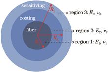
Peng Ding, Junbin Huang, Gaofei Yao, Hongcan Gu, Wen Liu, and Jinsong Tang
Objective A weak fiber Bragg grating(WFBG) array is fabricated online via wire drawing by a drawing tower, grating etching using a lithography platform, and primary coating by a ultra-violet(UV) curing device, wherein thousands of WFBGs are multiplexed. A WFBG array has the tensile strength of an ordinary fiber because of the array with no fusion point. It can be coated directly outside the UV-curable coating layer of the array to increase the underwater acoustic sensitivity and form hydrophones, which is expected to result in a towed line array with fine size, large aperture, and strong gain. There are two types of traditional theoretical analyses in case of a WFBG secondary coating. The first method is the two-layer model, which considers the fiber and the primary coating as the first layer and the second coating layer as the second layer. The two-layer model is considerably rough because of the small difference in fiber diameter, primary coating thickness, and secondary coating thickness. The second method is the three-layer model, which comprises an optical fiber layer, a primary coating layer, and a secondary coating layer. The stress values associated with the primary and secondary coating layers are directly equal to the external sound pressure, which exhibits a large error of fiber strain. In this study, a three-layer model according to the actual structure of the WFBG hydrophone with secondary coating is established. Further, the functional relation between the strain of the fiber layer and change in sound pressure can be established according to the boundary conditions of stress and displacement. The phase change law of optical pulse transmission in a fiber affected by sound pressure is studied, which provides the theoretical support required for the preparation of a WFBG hydrophone with secondary coating sensitization.Methods In this study, a three-layer model for a WFBG hydrophone is established according to the actual structure comprising an optical fiber layer, a primary coating layer, and a secondary coating layer. The undetermined coefficients are used to obtain the stress, strain, and radial displacement in the three-layer regions, which are obtained according to the boundary conditions of radial displacement, radial stress, and axial stress. Further, the law of fiber strain affected by acoustic pressure is obtained, and the phase change rule with respect to the optical pulse in an optical fiber can be understood. High-density polyethylene (HDPE) is considered to be the secondary coating material in the theoretical model simulation, and a 0.4-mm-diameter HDPE-coated WFBG hydrophone is prepared. A 50-m-long WFBG hydrophone is rolled into a 6-cm-diameter ring and placed in a vibrating liquid column. The phase-sound pressure sensitivities of the hydrophone are measured at frequencies of 5, 7.5, 10 Hz, which are compared with those of the bare WFBG array to verify the sensitization effect of the hydrophone.Results and Discussions The simulation results indicate that the phase-sound pressure sensitivity of the hydrophone increases with the increasing secondary coating thickness. The sensitivity remains unchanged when the radius of the hydrophone reaches 1 mm[Fig.2(a)]. The sensitivity decreases with the increasing elastic modulus of the secondary coating material [Fig.2(b)], indicating that the larger the elastic modulus, the smaller will be the axial strain caused by sound pressure change and the smaller will be the phase change. The sensitivity increases with the increasing Poisson’s ratio[Fig.2(c)], indicating that the larger the Poisson’s ratio, the greater will be the transverse strain caused by sound pressure change and the greater will be the phase change. Theoretical analysis shows that sensitivity can be increased by 19.8 dB with an HDPE coating (Fig.3). The sensitivities of a 50-m-length bare WFBG array are -176.26 dB (1 rad·μPa -1)@5 Hz(Fig.6), -170.53 dB@7.5 Hz(Fig.7), and -160.96@10 Hz(Fig.8), whereas those of a 50-m-long and 0.4-mm-diameter HDPE-coated WFBG hydrophone are -132.74 dB@5 Hz(Fig.9), -126.93 dB@7.5 Hz(Fig.10), and -126.04 dB@10 Hz (Fig.11). When compared with the sensitivities of the bare WFBG array, the comprehensive sensitivity of WFBG is greater by approximately 40 dB (Table 2). Conclusions Thus, a WFBG hydrophone with secondary coating sensitization is proposed in this study. The selection of secondary coating material and thickness of the WFBG array is guided by a three-layer composite stress model. Simulation results show that HDPE (elastic modulus is 0.84 and Poisson’s ratio is 0.38) as the coating material can increase sensitivity by 19.8 dB. The sensitivities of a 0.4-mm-diameter WFBG hydrophone under frequencies of 5, 7.5, 10 Hz are measured using a vibrating liquid column. The overall sensitization effect is approximately 40 dB. Simulation and experimental results show that a high-sensitivity hydrophone can be obtained by coating a WFBG array with 50-m grating spacing via HDPE. The sensitivities are -132.74 dB@5 Hz, -126.93 dB@7.5 Hz, and -126.04 dB@10 Hz, and the fluctuation in frequency response is 6.7 dB.
Apr. 26, 2021Vol. 48 Issue 9 0906003 (2021)
Jinsong Xiang, and Shaohua Zhang
Objective Because of the extremely long communication link in deep space, the detection signal is easily affected by channel characteristics such as background light noise and delay jitter, and the output signal-to-noise ratio (SNR) is very low, which leads to the poor synchronization performance of a receiver. Therefore, it is very important to achieve precise synchronization at low SNR. In general, pulse position modulation (PPM) slot synchronization is mainly in the form of closed-loop tracking, such as phase-locked loop and early-late gate, and the system design is complex. According to the estimation of timing error of the training sequence inserted periodically, the open-loop synchronization is realized, which will waste certain transmitting power. Using the maximum likelihood synchronization method of the guard slot, this method can reduce the computational complexity effectively, however, the bit error rate (BER) will be obvious when the signal power is high. The slot synchronization method of a photon detector array based on photon arrival time measurement requires complexity that is still high. The clock synchronization method based on the fast Fourier transform (FFT) has fast computing speed and the support of underlying hardware. It is suitable for real-time signal processing and has been widely used in wireless communication and optical fiber communication. However, the error of the signal parameters obtained directly from the FFT line spectrum is sometimes very large, which requires frequency correction. However, the single frequency correction method is not robust. We will apply the classical FFT algorithm to the photon-detected PPM communication system in slot synchronization. A method of PPM open-loop synchronization is proposed by selecting the optimal value from the Quinn, Jacobsen, and MacLeod algorithms. To solve the problem that the existing data recovery methods are inaccurate, a data recovery method based on correlation detection is proposed.Methods The optical PPM signal is sampled asynchronously more than twofold and passed through the FFT, but the error of the signal parameters obtained directly from the FFT line spectrum is sometimes very large, which requires refinement of the frequency estimation. The common frequency correction methods are Rife, Quinn, MacLeod, and Jacobsen. However, the robustness of a single frequency correction method is poor. In this paper, we estimate the initial frequency deviation of the PPM signal using Quinn, Jacobsen, and MacLeod algorithms, and then obtain the time delay deviation. According to the frequency deviation and time delay deviation estimators, the photon number of the PPM signal is recovered through a correlation operation, and then three sets of slot logarithmic likelihood ratio sequences are obtained. Finally, the sequence with the largest standard deviation is selected from these three sets of time slot logarithmic likelihood ratio sequences as the input of the error correction decoder.Results and Discussions The classical FFT method is applied to slot synchronization of a photon detection PPM communication system. Compared with existing PPM slot synchronization methods, the slot synchronization method proposed in this paper does not need to insert training series, is not limited by the number of guard slots, the system structure is simple, easy to implement by hardware, and the operation speed is fast, PPM slot synchronization can be achieved at very low optical power. The method estimates the initial frequency offset of the signal using the Quinn, Jacobsen, and MacLeod algorithms, and then obtains the time delay deviation of the signal, PPM open-loop synchronization is realized by selecting the optimal value from three ratio methods according to the maximum standard deviation criterion of logarithmic likelihood ratio of slots. Compared with the single ratio method, this method is more robust, and the calculation time is only 1.13 times that of the single ratio method. In this paper, the photon number recovery method based on correlation detection is proposed to verify the high-performance optical PPM experiment based on a multipixel photon counter (MPPC). For 64PPM and fourfold PPM slot frequency asynchronous sampling, the method in this paper only needs to detect 1.33 photons per signal pulse on average, which can make BER less than 10 -5. Conclusions In this paper, an experimental optical PPM communication system based on MPPC is established, and the classical FFT method is applied to the photon detection PPM communication system. Through the maximum standard deviation criterion of the logarithmic likelihood ratio of the slot, the optimal value is selected from the three ratio methods to realize the open-loop synchronization of the PPM slot. Compared with the existing PPM slot synchronization method, the PPM open-loop synchronization method proposed in this paper does not require the insertion of training series and is not limited by the number of guard slots. The system is simple in structure, easy to implement by hardware, and fast in operation speed. PPM slot synchronization can be achieved at extremely low optical power. Compared with the single ratio method, the slot synchronization method is more robust, and the operation time is only 1.13 times that of the single ratio method. In this paper, a photon number recovery method based on correlation detection is proposed to verify the high-performance optical PPM experiment based on MPPC. The experimental results show that the BER performance of the proposed correlation detection algorithm is 0.65 dB and 0.50 dB compared with the ideal simulation data, for the asynchronous sampling signals with twofold and fourfold PPM slot frequency, respectively. For 64PPM and fourfold PPM slot frequency asynchronous sampling, the proposed method in this paper only needs to detect 1.33 photons per signal pulse on average, which can make BER less than 10 -5.
Apr. 27, 2021Vol. 48 Issue 9 0906004 (2021)
Zufeng Chen, Faxing Zuo, Liang Hu, Yi Jin, Jianping Chen, and Guiling Wu
Objective Ultraprecise time synchronization plays an important role in scientific research and commercial applications. Owing to the advantages of optical fiber’s low transmission loss, high reliability, and stability, optical fiber time synchronization has been considered as a promising solution for high-precision time synchronization. This paper adopts a highly precise optical fiber time comparison scheme proposed by Shanghai Jiao Tong University, which uses bidirectional time-division multiplexing transmission over a single fiber with the same wavelength (BTDM-SFSW). The scheme can effectively suppress both effects of the Rayleigh backscattering and dispersion-induced bidirectional asymmetry simultaneously, whereas it does not achieve time synchronization. This study, which realizes time synchronization, adopts the scheme to obtain the time difference between two clocks and uses the clock servo technique to eliminate the time difference between two clocks.Methods A time synchronization experimental system is set up based on the BTDM-SFSW time comparison scheme and clock servo technique (Fig. 1). After using the BTDM-SFSW time comparison scheme to obtain the time difference between two clocks (Fig. 2), the difference between setpoint value and the time difference is used as error signal of proportion-integral-differential (PID) controller (Fig. 3), which is processed and summed by proportional, integral, and derivative units to obtain the output of the controller. The voltage-controlled crystal oscillators (VCXO's) frequency is adjusted according to the frequency correction algorithm and the controller’s output to change the phase of one pulse per second (1PPS) derived from the pulse per second (PPS) generator. New 1PPS is used by BTDM-SFSW time comparison to obtaining a new time difference between two clocks, which is treated as the feedback value of the controller. The above steps constitute a feedback control for the elimination of the time difference.The time synchronization system adopts the same optical fiber and wavelength, which fully guarantees delay symmetry of the bidirectional link. After the calibration of time-synchronized terminals, there is no need to calibrate the optical fiber link.Results and Discussions In an air-conditioned laboratory, time-synchronized terminals are connected by a 1 m optical fiber, and the calibration of terminals is completed by modifying the PID controller’s setpoint value to adjust the convergence position of the time difference so that the average value of time difference after synchronization is stabilized near zero. After calibration, the PID parameters such as setpoint value, proportional gain, integral time, and derivative time are no longer changed. The average value of time difference after time synchronization is less than 1.5 ps, 3 σ time difference is less than 228 ps (Fig. 4 (a)), and time deviation (TDEV ) of time difference is better than 15 ps/s and 1.5 ps/104 s respectively (Fig. 4 (b)). Compared with TDEV of time difference without synchronization, the long stability of time difference after synchronization is significantly improved.Time-synchronized terminals, which have been calibrated over a 1 m optical fiber, are connected by 30, 50, 80, and 100 km standard single-mode optical fibers respectively to perform experiments. The average value of time difference after synchronization is less than 10 ps (Fig. 5). Results of the experiment show that the system can achieve high-precision time synchronization over optical fiber links, that have different lengths by using a short optical fiber to complete calibration of terminals without calibration of the optical fiber link.The field test is conducted over a standard single-mode optical fiber link between Minhang and Xuhui campuses of Shanghai Jiao Tong University. The length of the optical fiber link is about 60 km, and the total attenuation of the link is about 24 dB. The average value of time difference after time synchronization is less than 9 ps, 3 σ time difference is less than 285 ps (Fig. 6 (a)), and TDEV of time difference is better than 16 ps/s and 7 ps/104 s respectively (Fig. 6 (b)). Compared with the TDEV of time difference after synchronization using a 1 m optical fiber to connect terminals, the short stability of the field test’s time difference does not change significantly, whereas the long stability worsened over the field optical fiber link. It is reasonable since the long-term stability is mainly related to the fluctuations of propagation delay asymmetry caused by variations in temperature and wavelength difference, which are proportional to optical fiber length. The “bump” of TDEV near 10 s is caused mainly by hysteresis of VCXO frequency adjustment. It indicates that the steering corrections are unable to compensate for the frequency drift completely at certain averaging times.Conclusions In this study, a time synchronization system is designed based on the BTDM-SFSW time comparison scheme and clock servo technique. The system takes advantage of the high bidirectional transmission delay symmetry of BTDM-SFSW time comparison without calibration of the optical fiber link. Laboratory and field optical fiber link tests are conducted, and results of the experiment show that after completing calibration of time-synchronized terminals, the average value of time difference after synchronization is less than 10 ps over different lengths of optical fiber links, and using a field optical fiber link of about 60 km, the average value of time differences after time synchronization is less than 9 ps, 3σ time difference are better than 285 ps, and TDEV is better than 16 ps/s and 7 ps/104 s respectively.
Apr. 26, 2021Vol. 48 Issue 9 0906005 (2021)
Cuiwei Liu, Jianjun Yu, Liangming Xiong, and Jie Luo
Objective With the advantages of large available bandwidth and minimum interference in existing wireless services, millimeter-wave (mm-wave) technology can be widely used in future space communication or wireless communication. In previous research, the generation schemes of photon-assisted mm waves have mainly included: direct modulation technology, external modulation technology, and optical heterodyne technology. In order to overcome the bandwidth limitation of devices and meet the requirements of low-cost, the generation of vector mm waves with low radio frequency (RF) signals and intensity modulators has become a research hotspot. However, this method suffers from two main drawbacks, namely the phase multiplication and the cost of the system. To improve the above-mentioned problems, we generate a carrier suppression mm-wave signal with an intensity modulator. We also consider the carrier suppression vector mm-wave signal for achieving four-wave mixing (FWM) in a highly non-linear dispersion-shifted fiber to increase the frequency of the mm-wave. We use a balanced precoding algorithm to demodulate the distortion of the signal during transmission. That is, the complex and expensive I/Q modulator, as well as the bandwidth requirements of the optoelectronic devices is avoided. Furthermore, a single side band (SSB) vector mm-wave signal that can be delivered over relatively long fiber transmission distances is generated. Based on our scheme, we propose and experimentally demonstrate a 2-Gbaud QPSK vector mm-wave signal generation at 72 GHz by six-fold frequency. A mm-wave signal transmission over a 15-km fiber and with 1-m wireless for a bit error rate (BER) below the hard decision-forward error correction (HD-FEC) threshold of 3.8×10 -3 is also realized. Methods We propose a new scheme to generate a six-fold requency vector mm-wave signal based on FWM and balanced precoding. To achieve six-fold frequency, we use carrier suppression modulation with a single intensity modulator and FWM with a 1-km highly non-linear dispersion-shifted fiber. Combined with balanced precoding, a 72-GHz carrier frequency quadrature phase shift keying (QPSK) vector mm-wave signal is generated. Maintaining the signal quality is essential for reducing the system cost. We demonstrate, via experiments, the generation of a 2-Gbaud 72-GHz QPSK vector mm-wave signal, and discuss the effects of baud rate and fiber transmission length of the QPSK signal on the signal.Results and Discussions The BER versus photodetector (PD) input power curves after back-to-back (BTB) and 15-km fiber transmission are almost the same (Fig. 7), indicating a lack of dispersion penalty after the 15-km fiber transmission. To further explore the transmission performance of the signal in the fiber, we determine (via experiments) the maximum receiver optical power required for achieving the BER at 3.8×10 -3 under different fiber lengths (Fig. 9). As shown in Fig.9, the optical power is remained at -6.3 dBm after -6.3 dBm and the QPSK signal baud rate is ≤2.5 Gbaud. Conclusions We demonstrate to the generation of a six-fold frequency vector mm-wave signal using precoding. In our scheme, we generate a 72-GHz V-band vector mm-wave signal with oscilloscope (OSC) and FWM using our designed electrical signals. We demonstrate (via experiments) the generation of a 72-GHz 2-Gbaud QPSK signal. After 15-km fiber transmission and 1-m wireless transmission, when the baud rate of the signal is ≤2.5 Gbaud, the HD-FEC algorithm can achieve error-free transmission. The results revealed that the vector mm-wave signal based on this scheme exhibits excellent transmission performance. As indicated above, this scheme overcomes the bandwidth limitation of devices, meets the requirements for low-cost devices, and reduces the frequency of the RF signal. Our proposed scheme with six-fold frequency combines the advantages of our two aforementioned categories of photonic vector mm-wave generation schemes. The authors believe that expensive electronics operating at high carrier frequencies with a bandwidth limitation can be avoided. That is, photonics-aided mm-wave technology has been widely applied to the generation and processing of mm waves. The millimeter ROF delivery based on highly efficient spectrum modulation will be a promising method of developing larger capacity links than currently available links.
May. 17, 2021Vol. 48 Issue 9 0906006 (2021)
Qinghe Yuan, Hongqi Jing, Suping Liu, Xiaoyu Ma, and Xiaohui Ma
Objective The high power and high beam quality of tapered semiconductor laser output have led to a recent increase in research conducted in this field. Two guided wave modes are mainly used in semiconductor lasers: refractive index and gain waveguides. Little attention is paid to the gain waveguide owing to its unstable mode; instead, refractive index waveguide structures are often used in tapered semiconductor lasers. Although a tapered semiconductor laser with a refractive index waveguide structure can output high power and high beam quality, the product is similar to that of a high-power wide-contact semiconductor laser. The beam is unstable at high power output and is prone to twisting and causing filamentation. This phenomenon occurs for two reasons. The first is that mode filtering is not ideal in the ridge waveguide part, and the beam injected into the tapered area is not the fundamental mode. The second is that the refractive index changes in the tapered amplification area owing to thermal induction or spatial hole burning, which causes the beam to self-focus. In present studies, the difference in the output characteristics of the gain and refractive index waveguide structures for a tapered semiconductor laser is analyzed. Although the output power of a laser with a gain waveguide structure shows a slight decrease, its beam quality is significantly improved. This study provides a reference for the design of tapered semiconductor lasers with high power and high beam quality.Methods In this study, the professional optical waveguide simulation software, RSoft, was used to compare and analyze the influences of the gain and refractive index waveguide structures on the output characteristics of a tapered semiconductor laser. First, the structural parameters of a tapered semiconductor laser including the length and width of the single-mode region as well as the length and angle of the tapered region were determined through the relevant theoretical analysis. Then, RSoft was applied to the model for simulation. The near- and far-field distributions, beam quality factor and power-current-voltage characteristics under different guided wave modes were finally determined. In addition, to verify the accuracy of the simulation results, tapered semiconductor lasers with gain and refractive index waveguide structures were fabricated separately, and the beam quality factor was measured using the knife-edge method.Results and Discussions In the analysis of the near-field distribution, the optical field distribution on the back cavity surface of the gain waveguide structure laser was relatively smooth with no high spikes. In contrast, that of the refractive index waveguide structure laser was relatively rough, with numerous small spikes appearing in the single-mode region (Fig. 2). Furthermore, the optical field distribution on the light-emitting surface of the gain waveguide structure laser was relatively uniform with no high-intensity spikes; that of the laser with a refractive index waveguide structure, however, showed two high-intensity spikes (Fig. 3). The far-field characteristic analysis showed a far-field divergence angle of about 2°×40° (slow axis × fast axis) in the gain waveguide structure, and for the refractive index waveguide structure, the angle was about 8°×40°. The far-field divergence angle of the refractive index waveguide structure laser in the direction parallel to the PN junction was larger than that of the gain waveguide structure laser, and the angle was relatively small. The far-field of the gain waveguide structure laser showed only one spot, whereas that of the refractive index waveguide structure laser exhibited two nearly identical spots (Fig. 4). In addition, the beam quality factor of our fabricated device was measured (Fig. 5). In the range of 0--1.5 W, the beam quality factor of the tapered laser with a gain waveguide structure was smaller than that with a refractive index waveguide structure when the output power was constant. Furthermore, the power-current-voltage analysis result indicated that under a voltage of 1.55 V, the output optical power of the tapered laser with a gain waveguide structure was 820 mW, whereas that with a refractive index waveguide structure was 890 mW. Therefore, the output optical power difference between these two lasers was 70 mW (Fig. 6). The slope efficiencies of the gain and refractive index waveguide structures were calculated to be 0.932 W/A and 1.07 W/A, respectively.Conclusions In this study, the influences of the gain and refractive index waveguide structures on the output characteristics of a tapered semiconductor laser are studied by simulation and experimentation. The results show that under the same voltage condition, the output power of the tapered laser with a gain waveguide structure is relatively lower than that with a refractive index waveguide structure. However, the light field distribution on the output facet is more uniform. The lower output power can effectively reduce the spatial hole burning effects and result in a better far-field distribution. The light confinement effect is stronger in the refractive index waveguide structure than that in the gain waveguide structure, which causes light reflected from the front cavity surface of the tapered laser to be limited to both sides of the single-mode region and prevents dissipation. The light reflected back again enters the tapered area for amplification, resulting in optical power with relatively high output. In the gain waveguide structure, however, the weak light confinement effect causes a large part of the light reflected from the front cavity surface to be lost. Because the light does not re-enter the tapered area for optical amplification, its output optical power is relatively low. Moreover, the strong confinement effect of the refractive index waveguide structure on the light causes most of the light reflected from the front cavity surface to propagate along the back cavity surface through scattering. This in turn causes a relatively messy distribution of the optical field on the back cavity surface. The light reaching the back cavity surface, which is a high-order transverse mode, is reflected from the back cavity surface and propagates along the front cavity surface outside the single-mode area. If its propagation angle is smaller than the tapered angle of the tapered laser, part of the light will likely re-enter the tapered part to strongly affect the beam quality of the device.
May. 06, 2021Vol. 48 Issue 9 0901001 (2021)
Hanzhao Li, Weiwen Qian, Lu Liu, Huilian Ma, and Zhonghe Jin
Objective A resonant fiber optic gyroscope (RFOG) is a rotation rate sensor based on the Sagnac effect. The rotation rate is measured by determining the resonant frequency difference between the clockwise and counterclockwise waves propagating in a multiturn fiber ring resonator. Since the Sagnac effect is very weak, signal modulation and demodulation techniques are indispensable for improving the detection accuracy of the RFOG. The sinusoidal wave-phase modulation and demodulation techniques are widely used in the RFOG, in which the modulation index is set as 2.405 to reduce the backscattering noise. The modulation frequency is conventionally optimized to maximize the demodulation slope at the resonant point, which yields the highest sensitivity. However, the shot-noise-limited theoretical sensitivity of the RFOG depends on the signal-to-noise ratio (SNR) rather than the most sensitive working point. Angle random walk (ARW) is one of the basic parameters of the RFOG, which is used to evaluate the shot-noise limit.Aiming at the optimum theoretical ARW, the influences of the modulation parameters, including the modulation index, modulation frequency, and demodulation phase, on the theoretical ARW are analyzed. This study provides insights into the optimization of the modulation parameters to improve the theoretical sensitivity of RFOGs. Our experiments verify the simulation results.Methods Here, we introduce the basic operating principle of the RFOG based on the sinusoidal phase modulation and demodulation techniques. Thereafter, the theoretical ARW is derived in detail. The relationship between the theoretical ARW and the modulation parameters is analyzed. We find that the modulation parameters for the optimum ARW are different from those for the most sensitive working point. Subsequently, we set up a practical RFOG system based on the sinusoidal phase modulation and demodulation techniques and determine the influences of the modulation parameters on the ARW. We employ the power spectral density (PSD) analysis method to calculate the ARW of the gyro output data.Results and Discussions In the practical RFOG system, the diameter of the fiber ring resonator is 12 cm and the total fiber length is 29 m. The measured fineness is 14.7. All the simulation results are obtained using the same fiber ring resonator as that in the practical RFOG system, and the peak output power of the resonator is 30 μW. Figure 5 shows the relationship between the amplitude of the demodulation output at a given rotation rate and the modulation-demodulation parameters. Two modulation indexes are calculated, i.e., 1.080 and 2.405. The relationship between the maximum demodulation output and the modulation parameters is further investigated, as shown in Fig. 6. When the modulation index is greater than 1, the maximum demodulation output remains almost unchanged with the variation of the modulation frequency. For example, when the modulation index is 1.1, the optimal modulation frequency is approximately 180 kHz and the maximum amplitude of the demodulation output corresponding to a rotation rate of 1 (°)/s is approximately 1.44×10 -3. When the modulation index is 2.2, the optimal modulation frequency is 80 kHz and the maximum amplitude is 1.5×10 -3. The difference is only approximately 4%. This is because when the modulation index is greater than 1, the maximum demodulation slope at the resonant point remains almost unchanged as the modulation index increases. The RFOG based on the sinusoidal modulation-demodulation technique can achieve the optimum theoretical sensitivity by resorting to match three parameters, including the modulation index, modulation frequency, and demodulation phase. The optimum sensitivity is related to the demodulation slope at the resonant point, as well as the output power of the fiber ring resonator. The relationship between the output power and the modulation parameters is shown in Fig. 7. It can be observed that the output power decreases as the modulation frequency or index increases. A set of optimal modulation-demodulation parameters (Figs. 8 and 9) related to the fiber ring resonator is observed, which enables the achievement of the best ARW. When the modulation frequencies are set as 1 MHz, 600 kHz, and 240 kHz, the calculated ARWs are 0.010 (°)/h, 0.007 (°)/h, and 0.005 (°)/h, respectively; for the practical RFOG system, the measured ARWs are 0.0124 (°)/h, 0.0072 (°)/h, and 0.0052 (°)/h (Fig. 10), respectively. Conclusions An RFOG based on the sinusoidal modulation and synchronous demodulation technique is optimized to improve its shot-noise-limited theoretical sensitivity. The optimal modulation parameters, including the modulation frequency, modulation index, and demodulation phase, corresponding to a certain fiber ring resonator are obtained. Thereafter, an experimental system is set up to verify the simulation results. When the peak output power of the fiber ring resonator is 30 μW, the measured ARW of the RFOG is 0.0052 (°)/h, which is close to the theoretical value.
May. 06, 2021Vol. 48 Issue 9 0901002 (2021)
Haiyue Pang, Zhaoyun Li, Huan Li, Zhiyong Tao, and Yaxian Fan
Objective Optical frequency combs (OFC) consist of a series of evenly spaced discrete spectral components that maintain high spectral coherence. It can be applied in many fields, such as metrology, spectroscopy, optical arbitrary waveform generation, THz generation, microwave photonics, and optical communications. Among the available optical comb technologies, OFC based on semiconductor lasers provides suitable combs with competitive costs and efficiency. Vertical-cavity surface-emitting laser (VCSEL) is a single-longitudinal mode semiconductor laser. Compared with an edge emitter, VCSEL has some advantages, such as on-wafe test capability, lower energy consumption, lower manufacturing cost, and circular output beam. VCSEL can emit in two orthogonal linear polarization modes. Polarization switching between these modes can be found when changing the temperature or bias current applied to the VCSEL. These properties make them appropriate for OFC generation. Dual-polarization OFC-based VCSEL can be generated due to the special polarization properties. Further efforts are required to improve OFC-based on VCSEL, especially to expand the optical span while maintaining the existing advantages. In this study, we proposed a scheme for generating broadband dual-polarization OFC based on a 1550-nm VCSEL under optoelectronic feedback, opening perspectives for polarization-sensitive sensing and multicarriers optical sources for polarization-division multiplexing optical communications.Methods We proposed and analyzed theoretically a scheme for generating a 500-GHz dual-polarization optical frequency comb based on a 1550-nm VCSEL under optoelectronic feedback. Besides, we numerically investigated the influences of optoelectronic feedback parameters on the performances of the generated optical frequency comb. The proposed model considered the optoelectronic feedback based on the rate equations of the spin-flip model of 1550-nm VCSEL. First, we proposed a schematic diagram of a broadband dual-polarization OFC generation based on a 1550-nm VCSEL under optoelectronic feedback. Then, we analyzed the output power versus normalized bias current curves of the two modes with orthogonal polarizations of the free-running 1550-nm VCSEL that is without optoelectronic feedback. After that, optoelectronic feedback effects on the polarization dynamics of 1550-nm VCSEL under different optoelectronic feedback parameters are theoretically investigated using the spin-flip model. In the next step, we analyzed the time series and optical spectra of the two linear polarization modes with orthogonal directions of 1550-nm VCSEL under a certain normalized bias current and optoelectronic feedback time with different optoelectronic feedback coefficient values. In addition, we analyzed the optical and power spectra of the two linear polarization mode outputs of 1550-nm VCSEL with different optoelectronic feedback coefficients.Results and Discussions The results showed that two linear polarization modes with orthogonal directions of the 1550-nm VCSEL under optoelectronic feedback can be controlled by adjusting the optoelectronic feedback parameters. When the bias current or optoelectronic feedback parameters are changed under 1550-nm VCSEL, the polarization conversion of the Y- and X-polarization occurs (Fig. 3). Besides, we obtained that the dual-polarization optical frequency comb with Y- and X-polarization can be achieved under certain conditions of optoelectronic feedback parameters (Fig. 4). Within a certain range of optoelectronic feedback parameters, the optical spectral bandwidth of the Y- and X-polarization optical frequency comb increases with an increase in optoelectronic feedback coefficient (Fig. 5), and the corresponding power spectrum becomes flatter with an increase in optoelectronic feedback coefficient (Fig. 6). By adjusting the optoelectronic feedback coefficient and time, we obtained broadband dual-polarization optical frequency comb with flat spectral lines, pure comb lines. The spectral widths of the Y- and X-polarization optical frequency combs were more than 250 and 500 GHz within the amplitude range of 10 dB, respectively (Fig. 5).Conclusions In this study, we proposed and analyzed theoretically a novel scheme for generating a 500-GHz dual-polarization optical frequency comb based on a 1550-nm VCSEL under optoelectronic feedback. It is shown that two orthogonal linear polarization optical frequency combs can be obtained and have comparable span and power under certain optoelectronic feedback conditions. The 10-dB spectral width of optical frequency combs of the Y- and X-polarization larger than 250 and 500 GHz can be achieved in the 1550-nm VCSEL subject to optoelectronic feedback under certain optoelectronic feedback parameter conditions, respectively. An appropriate increase in optoelectronic feedback coefficient in 1550-nm VCSEL can increase 10-dB spectral width. This increase is essential for enhancing the performance of OFCs generated by 1550-nm VCSEL under optoelectronic feedback for polarization-sensitive sensing and polarization-division multiplexing optical communications.
May. 17, 2021Vol. 48 Issue 9 0901003 (2021)
Zebin Feng, Yi Zhou, Rui Jiang, XiaoQuan Han, Xiangyu Xu, and Bin Liu
Objective Excimer lasers are widely used in industrial, medical, and scientific fields because of their short wavelength, high power, and narrow line width. Especially rare gas halogen excimer laser, because of its high peak output power, high single pulse energy, and ultraviolet wavelength, has become the main laser source in the semiconductor lithography industry. Its energy is one of the three key parameters (energy, linewidth, and wavelength) of excimer laser for photolithography, which directly determines the processing accuracy, yield, and key dimensions of semiconductor lithography. When studying the energy of an excimer laser, the closer the model approaches the actual law of light output energy, the more conducive to the study. The output energy model of an excimer laser is the basis for studying and controlling the energy characteristics of the laser. Discharge process of excimer laser is a complex nonlinear process, which leads to the accuracy of laser discharge energy model based on discharge dynamics is difficult to meet the needs of simulation research and control algorithm design. In this paper, the method based on deep learning was applied to identify the energy mode of excimer laser to avoid the inaccuracy of theoretical modeling.Methods The development of deep learning theory has become more and more complete. It has become a tool and has been widely applied. Among them, recurrent neural network (RNN) is an important branch in the field of deep learning. It has been widely used in language recognition, machine translation, text analysis and other fields. In recent years, circulating neural networks abroad, especially its variant gate recurrent unit (GRU), has been applied to model recognition, trend prediction and other fields. In this paper, the gated recurrent unit network was used to identify the discharge energy model of the excimer laser. Firstly, based on the characteristics of the excimer laser energy, the discharge voltage and discharge interval were selected as the input of the established gating recurrent unit network. Then, according to the characteristics of the gated recurrent unit network and the excimer laser energy, a neural network suitable for energy model identification of excimer laser was established. When using the GRU network to identify the laser light energy model, a burst pulse energy sequence was used as a time sequence. Finally, the back propagation through time (BPTT) was used to train the established GRU network.Results and Discussions Using GRU to learn the energy model of excimer laser requires a lot of data. The data was taken from a KrF excimer laser that produces laser of 248 nm, which worked at a repetition frequency of 4 kHz. Since the wavelength of the excimer laser also affects the energy data, in the course of the experiment, the wavelength was controlled at 248.327 nm using feedback technology. Energy data of the laser was collected under discharge high voltages of 1400 V, 1450 V, 1550 V, and 1600 V, respectively. In order to make full use of the data, at each training, the data under different discharge voltages was randomly selected to train GRU. The termination condition was set as 100000 trainings or the maximum error less than 0.15 mJ. The maximum error of model under each high voltage was less than 0.15 mJ (Fig. 6). Since the energy center value was 10 mJ, the relative error was less than 1.5%. The change of the maximum error in the training process indicates that the GRU neural network converges during the training process (Fig. 7). The data outside the training set was used to validate the model. The model obtained by training was used to calculate the laser light energy when the high voltage was 1550 V, and the comparison between the obtained energy value and the energy value collected on the actual laser after processing (1) is shown in Fig.8. The energy obtained through the GRU neural network has a good coincidence with the energy of the actual pulse. Another verification data set was collected at laser working with repetition frequency of 1, 2, 3, and 4 kHz. The maximum error between the model data and the actual laser data was less than 0.13 mJ under different repetition frequencies, that is, the relative error was less than 1.5% (Fig. 10).Conclusions The energy model of excimer laser is a complex nonlinear model, which is difficult to get an accurate model from the theory. However, the actual research and application work need an accurate laser output energy model. In this paper, through the method of deep learning, GRU neural network was to identify the energy model. The verification results show that the maximum error between the pulse energy generated by the laser energy model identified by GRU neural network and the actual energy was less than 1.5%. The maximum error 1.5% is less than 2.74% of the required energy stability in dose control, which meets the simulation requirements of the model control effect. This method can accurately identify the laser energy model. Using the identified model can be more convenient for the simulation of energy control algorithm, so as to improve the energy stability control and dose accuracy control of excimer laser.
May. 17, 2021Vol. 48 Issue 9 0901004 (2021)
Yanan Zhang, Junqing Meng, Mingjian Wang, Zhenzhen Yu, and Weibiao Chen
Objective As a space active photoelectric remote sensing technology, lidar is of great significance to high-precision three-dimensional imaging, ground detection with high vertical resolution, and deep space exploration with high spatio-temporal resolution. For traditional spaceborne and high-altitude airborne lidars, laser signals with low repetition rate and high pulse energy and linear photoelectric detection technology were mostly used, which had problems such as high power consumption, large size, and low surface resolution. The development of single-photon detection technology can simplify the lidar system, and improve the detection sensitivity and detection efficiency. However, it also requires laser signals with different performance parameters. Laser with high repetition rates can increase the sampling frequency and describe the sampling target more accurately. And the laser signal with a narrower pulse width can reduce the detection error and improve the detection accuracy of the lidar. And the narrower linewidth laser, combined with the corresponding narrowband filter, can reduce the influence of background noise on the detector and improve the sensitivity of the detection system. In this paper, we report a compact single-frequency laser with high repetition rate, high pulse energy, and narrow pulse width output. We hope that our laser will be helpful to space active detection lidar based on single-photon detection technology.Methods In order to achieve narrow pulse laser output, electro-optic Q-switch is selected to obtain narrow pulses under 10 ns and generate high peak power laser. According to the theory of electro-optic Q-switched laser, the factors affecting the pulse width are analyzed: Nd∶YVO4 crystal with higher σ21τ value is selected to obtain a higher small signal gain; the cavity length is shortened and the pump power is increased to obtain a narrower laser pulse. In order to achieve a narrow linewidth laser output, a volume Bragg grating mode selection method is used to build a solid single-frequency laser. The laser is end-pumped by a continuous-wave laser diode. The semiconductor laser with a pigtail output has a center wavelength of 808 nm, which can realize an adjustable continuous output with a power of 0--15 W. The core diameter and numerical aperture of the fiber are 200 μm and 0.22. The collimating and focusing system is a combination of two plano-convex lenses with focal lengths of 15 mm and 23 mm, respectively. The 808 nm pump light is focused on the gain crystal. The actual spot radius of the focal point is about 300 μm. The 0 ° total reflection plane mirror M1 coated with 808 nm high-transmittance film and 1064 nm high-reflection film forms a flat cavity structure with the coupling output element reflective volume Bragg grating (RBG), and the physical cavity length is 48 mm. The polarization beam splitting is used as a polarizing element. The rubidium titanyl phosphate (RTP) crystal pair is used as an electro-optic Q-switch. PBS, RTP and the 1/4 wave plate together constitute the Q-switch of the laser. It adopts a voltage-increased electro-optic Q-switched method, and is driven by a high-frequency and high-voltage signal to realize the on and off switch of the optical circuit, forming a Q-switched giant pulse output.Results and Discussions At a repetition frequency of 10 kHz, when the pump power is 9.67 W, a laser output with an average power of 1.68 W is obtained (Fig. 4). The power instability within 3 h is 0.32% (Fig. 5). The output laser pulse width is 1.3 ns, and the pulse waveform is smooth (Fig. 6). The output wavelength is 1064.355 nm, and the line width is 1.0 pm (Fig. 8). According to the longitudinal mode interval formula Δλ=λ02/(2l'), the longitudinal mode interval is 8.6 pm in the condition of 65.7 mm optical cavity length in this experiment, which is larger than line width of the output laser. So the laser realizes single longitudinal mode output. The beam quality factor of two directions is Mx2=1.22 and My2=1.18 (Fig. 9).Conclusions A single-frequency solid-state laser with high repetition rate and narrow pulse width is introduced in this paper. The laser is end-pumped by a continuous-wave laser diode, Nd∶YVO4 crystal as gain medium, the RTP crystal pair as the electro-optic Q-switch, and RBG as output mirror. In a resonant cavity with an optical cavity length of 65.7 mm, the single-frequency laser output with a wavelength of 1064.355 nm is locked. And at a repetition frequency of 10 kHz, the laser has a pulse width of 1.3 ns, an average power of 1.68 W, and the beam quality of Mx2=1.22 and My2=1.18. The laser has a compact structure and achieves a narrow pulse width, a narrow line width, and a large energy laser output at a high repetition rate. It can be used as a laser radar emission source for single-photon detection, and can also be used as a seed source of the main oscillation power amplification system for amplification to achieve more long-distance detection.
Apr. 26, 2021Vol. 48 Issue 9 0901005 (2021)
Shuai Zhang, Bojia Jin, Xiangfeng Wang, Xiangyang Lei, Jian Wang, and Qiao Xu
Objective Potassium Dihydrogen Phosphate (KH2PO4) (KDP) crystal is currently the only nonlinear optical material that can be grown into a large aperture. It is widely used in inertial confinement fusion large aperture laser drivers as the terminal element of the harmonic conversion unit. The angle phase matching method is generally used to obtain high harmonic conversion efficiency so that the KDP crystal axis angle (the angle between the crystal plane normal and the crystal optical axis) is equal to the phase matching angle. From the growth to use, KDP crystals have gone through the following stages: slicing, processing, chemical coating, assembly, and adjustment. The crystal axis angle orientation accuracy is poorly controlled in the slicing stage, resulting in the crystal axis error of the milliradian. If the crystal axis error is encountered in the adjustment stage, it takes a considerable amount of time to adjust the crystal pose to achieve the best phase matching condition. This will increase the difficulty in assembly and reduce the efficiency of assembly and adjustment. It is also not conducive for batch assembly and large-scale production. Therefore, large-aperture laser devices require high-precision crystal axis angle correction during the processing stage.Methods To solve the problems of a large correction angle and high precision requirements in the angle error correction of the crystal axis of the KDP crystal in the processing stage, a correction strategy of an in-site detection feedback combined with multiple adjustment approximations is proposed. The crystal element is clamped on an adjustable angle vacuum chuck, and the noncontact distance measuring unit is erected above the crystal surface. With the movement of the machine tool slide, the measuring unit moves at a uniform speed relative to the crystal. The distance between the crystal surface and the probe is recorded at a fixed sampling frequency. Combining this distance and the movement distance of the machine tool sliding table, the crystal surface inclination angle can be obtained by the straight-line fitting. This angle is subtracted from the crystal axis angle error detected offline as the suction cup's adjustment value. After adjusting the suction cup, the proposed method is employed to detect the crystal surface tilt angle again. The above steps are repeated until the tilt angle of the on-site inspection crystal surface gradually approaches and converges toward the crystal axis angle error. Cutting the crystal surface with a diamond tool can complete the correction of the surface crystal axis angle. The crystal axis angle on the other side is corrected by turning over and cutting. The advantage of this method is that the correction accuracy does not depend on advanced adjustment tools, small reclamping errors, and precise linear axes.Results and Discussions The crystal axis correction on the first side of the KDP crystal is a process of an in situ detection and repeated iterative adjustments. The relevant parameters of three crystal samples during the iteration (Table 4) show that they gradually approached the crystal axis error angle after three rounds of adjustments. After the cutting is completed by the machine tool, the in situ detection result of 1#, 2#, and 3# crystal surface angles are -0.12 μrad, +0.76 μrad, and +0.82 μrad, respectively. In other words, the surface angle after cutting is controlled within 1 μrad [Fig. 8(b)]. The results show that the angle of in situ detection before cutting is equal to the change in the crystal surface angle before and after cutting. After cutting the other side of the KDP crystal, use a large-diameter interferometer to detect the crystal wedge angle. The angle of both sides is 0.2″(0.93 μrad) (Fig. 9), indicating that the crystal axis angles on both sides are the same after the second surface is cut. After completing the crystal axis angle correction of the three samples, the off-line precision crystal axis inspection equipment is used to detect the crystal axis angle error of the crystal. The results showed that the angle errors of the three crystal axes are +11.4 μrad, -9.0 μrad, and 0.59 μrad, respectively (Fig.10 and Table 5).Conclusions The proposed crystal axis error correction strategy of KDP crystal in the processing stage is based on the on-site detection feedback and multiple adjustment convergence. The correction requirements of the milliradian angle and microradian accuracy can be achieved using the proposed method. Results suggest that the roposed method can meet large-scale laser devices' requirements for KDP crystal axis use. The verification experiment results showed that only three rounds of iterative adjustment, the proposed method can quickly converge the angle error of the crystal axis from several millimeters to 20 μrad or less. Further analysis shows that the correction accuracy of the strategy is only determined by the length of the probe movement and the test accuracy. The larger the element diameter and higher the measurement accuracy, the higher the correction accuracy, which is particularly suitable for the crystal axis angle correction of the large-diameter KDP crystal element. Although the correction accuracy is unrelated with the suction cup adjustment accuracy, the correction efficiency is proportional to it. The higher the adjustment accuracy, the fewer the number of iterations and the higher the correction efficiency.
Apr. 26, 2021Vol. 48 Issue 9 0901006 (2021)
Weili Zhang, Cao Feng, Jian Sun, Rui Zhu, Jianguo Wang, Xuefeng Shen, Kui Yi, Meiping Zhu, and Jianda Shao
Objective The use of large steep lenses is an effective method of increasing the numerical aperture, which has an important impact on the resolution of the lithographic system. Because to the unique geometry of the large steep lens, the distance between the steep lens surface and the evaporation source varies depending on their relative position, and uneven distribution of the film thickness will inevitably occur in the radial direction of the lens. To meet the high demands of a lithographic system with a complex optical system, a steep lens must have a high transmittance over a wide range of incident angles. As a result, controlling the homogeneity of the film on a large steep lens has become a critical issue.As the planetary fixture rotates, the deposition angle will also change during the deposition. In this deposition, the growth state, packing density, and the roughness of film change accordingly, which leads to an uneven refractive index of the film. To investigate the deposition characteristics of the film on a steep convex lens, the mechanism of change of the deposition angle at different positions of the steep convex lens during the rotation of the planetary fixture was studied by computer simulation. The influences of the evolution of the deposition angle and the changes in the substrate temperature on the refractive index of the film were also studied. The results of experimental studies presented in this manuscript provided theoretical and practical guidance on the correction of the refractive index of the film on a steep lens.Methods Magnesium fluoride (MgF2), a commonly used coating material for deep ultraviolet optical thin films, was selected as the object of study. A single-layer film of magnesium fluoride was prepared by electron beam evaporation technology. The refractive index of the sample was obtained by spectral reflectance/transmittance envelope curve fitting method and the ellipsometer test method. The crystalline properties and morphology of the film were analyzed by X-ray diffraction and scanning electron microscopy, respectively. The evolution of the deposition angle during the rotation of the planetary fixture was obtained using software simulation.Results and Discussions According to the results of computer simulation, the average deposition angle of the film gradually increases from the center of the lens to the edge, and the range of distribution of the deposition angle gradually increases too. The influence of structural characteristics becomes more obvious. When the substrate temperature is 25 ℃, the deposition angle significantly affects the refractive index of the MgF2 film. As the deposition angle increases, the refractive index of the film gradually decreases. When the deposition angle increases from 0° to 85°, the refractive index of the MgF2 film at 200 nm decreases from 1.42 to 1.28, the change in the refractive index is 0.14, and the non-uniformity of the refractive index is 10.22%. When the substrate temperature is 200 ℃, the refractive index of the MgF2 film at 200 nm decreases from 1.45 to 1.39 with increasing deposition angle from 0° to 85°, the change in refractive index is 0.06 and the non-uniformity of refractive index is 4.51% (Fig.13). For the MgF2 film deposited at a substrate temperature of 25 ℃, the non-uniformity of the refractive index strongly affects the residual reflectivity of the 193 nm AR coating, increasing from 0.04% to 4.72%, whereas for the MgF2 deposited under high substrate temperature, the non-uniformity of the refractive index of the film layer increases the residual reflectivity of the 193 nm AR coating from 0.08% to 0.32% (Fig.13 and Fig.14).Conclusions The influence of the deposition angle on the uniformity of refractive index of the film was systematically studied. For the convex lens close to a hemispherical shape, the occlusion effect will be more significant with an increase in the deposition angle from 1.41° to 90°, as a result of some parts of the substrate cannot be covered with a film. For the MgF2 film, the non-uniformity of refractive index of the film at different deposition angles is 10.22% at 25 ℃, which significantly affects the optical properties of the 193 nm AR coating. When the substrate temperature increased to 200 ℃, the non-uniformity of refractive index of the film at different deposition angles decreased to 4.51%, while the effect of the deposition angle on the optical properties of the 193 nm AR coating dramatically decreased. It is shown that increasing the substrate temperature in a certain range can effectively increase the uniformity of refractive index distribution. The results of the experimental studies presented in this manuscript provided theoretical and practical guidance on the correction of the refractive index of the film on steep lens.
Apr. 30, 2021Vol. 48 Issue 9 0903001 (2021)
Xiuhua Fu, Xiaomin Lin, Gong Zhang, Ye Wang, and Jing Zhang
Objective This study introduces a new type of metal wire grid polarization element with high transmittance for transverse magnetic (TM) waves and a high extinction ratio. This polarization element has the ability to transmit incident light TM waves and to achieve the polarization effect of transverse electric (TE) wave reflection, which indicates an important application in stealth recognition and feature detection. Commonly used metal wire grid elements can be manufactured with single- or double-layer metal wire grid structures. The single-layer wire grid has high TM wave transmittance, although the extinction ratio is affected by the period, duty cycle, height, and other parameters. Although the double-layer metal wire grid structure has a higher extinction ratio, it suppresses the transmission of TM waves and causes a sharp drop in transmittance. In 2014, TM wave transmittance of more than 60% and the maximum extinction ratio of 22.2 dB were realized in a single-layer metal wire grid polarizer produced in Japan. In 2018, a single-layer metal wire grid polarization element manufactured by Shanghai Institute of Technical Physics of Chinese Academy of Sciences achieved TM wave transmittance of 83.3% and an extinction ratio of 10 dB. Presently, metal wire grid polarization elements reported at home and abroad cannot simultaneously meet the performance requirements of high TM wave transmittance and a high extinction ratio. Therefore, it is necessary to further study the structural design and preparation technology of these elements. In this study, a single-layer metal wire grid structure in the mid-infrared 3--5 μm band is developed, and the design and the preparation process of a polarization element are studied to improve the TM wave transmittance and the extinction ratio.Methods Effective medium theory (EMT) and rigorous coupled wave analysis (RCWA) were used to design the metal wire grid structure. According to the design theory of optical thin films, a multilayer anti-reflection film was designed to reduce the residual anti-reflection rate of the Si substrate and to further increase the transmittance of the TM waves. The finite difference time domain (FDTD) method was used to simulate the TM wave transmittance and the extinction ratio of the new grating structure. The polarization component structure was manufactured by electron beam evaporation and interference lithography. The surface quality of the film was improved by optimizing the deposition process of thin film materials, and the intermittent coating method was used to prepare the high-performance metal wire grid polarization element and to reduce the radiation temperature of the photoresist. The results were tested by the Fourier-transform infrared spectrometry and the finite difference time domain method.Results and Discussions A new type of polarization element structure is designed by combining a multilayer anti-reflection film with a metal wire grid to solve the requirements of high TM wave transmittance and high extinction ratios of a polarization element. In the mid-infrared 3--5 μm band, the average TM wave transmittance is 89.1% and the average extinction ratio is 21.9 dB. According to the design theory of optical film, the oxygen partial pressure is optimized during the SiO film deposition. At the center wavelength of 4 μm, the refractive index is 1.64, which reduces the refractive index of the SiO and improves the transmittance of the multilayer anti-reflection film. By changing the speed of the homogenizer to manufacture photoresists with different thicknesses and using the lift-off method to strip the metal wire grid, the thickness of the photoresist that can be completely stripped is determined. When using the intermittent coating method to vaporize metal Al with a certain thickness for several times at an interval of 10 min, the photoresist deformation and the shape error of the photoresist grid caused by radiant heat are both reduced, and the polarization performance of the manufactured metal wire grid element is improved.Conclusions A new type of polarization element is designed by combining a multilayer optical anti-reflection film with a metal wire grid, which reduces the residual reflectivity of the substrate and improves the transmittance of TM waves. The application of this film reduces the resonance effect between the substrate and the metal film. Thus, the energy enhancement caused by multiple reflection of TE waves is reduced, resulting in reduced transmittance of TE waves and an improved the extinction ratio. According to the experiment results, the influence of radiant heat from film deposition on the deformation of the photoresist during the preparation process is analyzed, and the deposition process parameters of the film are optimized. The preparation accuracy is improved, and a new type of metal wire grid polarization element is developed. After testing, the average TM wave transmittance and the average extinction ratio of the manufactured polarization device is 89.1% and 21.9 dB in the 3--5 μm band, respectively.
Apr. 29, 2021Vol. 48 Issue 9 0903002 (2021)
Huiyu Chen, Min Qian, Jingping Tang, Jimeng Cheng, Xin Wan, Junjiang Hu, Tao Meng, Yujing Shen, Shubin Chen, Lili Hu, and Wei Chen
Objective Inertial Confinement Fusion (ICF) is one of the technical approaches to realize controllable nuclear energies. The key to ICF is the high-peak power solid-state laser system. A large-sized, Nd-doped phosphate laser glass disk is the core gain material of the high-peak power solid-state laser system. In the gain media, the amplified spontaneous emission (ASE) and parasitic oscillation (PO) are generated, which can affect the energy storage efficiency and laser output capability of the high-peak power solid-state laser system. Now, the main method to absorb ASE and suppress PO is to clad the Cu 2+-doped glass at the peripheral edge of the Nd-doped phosphate laser glass. The edge-cladded Cu 2+-doped glass can absorb the reflected or scattered light at 1 μm and suppress the onset of parasitic oscillation. At first,the sealing edge-cladding method was applied to the elliptical slab of N21 Nd-doped phosphate laser glass and the N21 rectangular Nd-doped phosphate laser glass, immersed in the organic cooling medium in the high-power laser system. The sealing edge-cladding process involves first mixing a low melting temperature glass powder with a dispersant to form a slurry, then coating the slurry on the edge of the Nd-doped phosphate laser glass, and finally heat-treating the coated glass at below a temperature at which the Nd-doped phosphate laser glass is softened and deformed to bond the low melting temperature glass to the edge of the Nd-doped phosphate laser glass. However, this cladding method can create lots of defects such as bubbles, pits, and carbide at the cladding interface. These defects can increase the residual reflection (0.1 × 10⁻²-25 × 10-2), which can lead to a considerable increase in ASE and PO. With a rapid advancement in the laser technologies, the Nd-doped phosphate laser glass with better performance is obtained, such as the types of N31 and N41. They have relatively low soften temperatures. Also, the temperature for heat-treating coated glass is much lower than that of N21, which can result in more defects at the cladding interface. Therefore, the sealing edge-cladding method is not suitable for new types of laser glass. The monolithic edge-cladding method is developed which involves pouring the melted edge-cladding glass around the edge of the Nd-doped phosphate laser glass preheated in the mold. Now, we studied the monolithic edge-cladding of the N31 Nd-doped phosphate laser glass. The residual stress is a very important parameter of monolithic edge-cladding for engineering applications. In this paper, we discussed the residual stress in the monolithic edge-cladding of the Nd-doped phosphate laser glass.Methods We studied the influence factors on the residual stress in the monolithic edge-cladding of the Nd-doped phosphate laser glass with the simulation and experimental methods. The finite element analysis software of COMSOL Multiphysics 5.5 was used to simulate the melt bonding process of monolithic edge-cladding. We did some experiments on the cladding for various cladding temperatures and different thermal expansion coefficients of edge-cladding glass. Stress distributions of these cladded samples were measured with the high-precision imaging polarimeter, and the stress distributions were studied.Results and Discussions By simulation, the residual stress distributions between the Nd-doped phosphate laser glass and edge-cladding glass for different thermal expansion coefficients are shown in Figs. 4 and 5. They indicated that a mismatch between the thermal expansion coefficients of the Nd-doped phosphate laser glass and the edge-cladding glass can cause residual stress. Higher difference in the thermal expansion coefficients can give rise to higher residual stress. The residual stress distributions are similar but different in magnitude. The Nd-doped phosphate laser glass cladded with glass with a thermal expansion coefficient of α2 is chosen to demonstrate the characteristics of residual stress distribution, as shown in Figs. 6, 7, and 8. The residual stress distributions for different cladding temperatures are shown in Figs. 9, 10, 12, and 13. They indicated that the cladding temperature can also lead to residual stress. Higher cladding temperature can give rise to higher residual stress. The residual stress distributions are also similar but different in magnitude. The Nd-doped phosphate laser glass cladded with T=1273.15 K is chosen as a representative to demonstrate the characteristics of residual stress distribution shown in Figs. 14, 15, and 16. By experiment, the residual stress distributions for cladding with different thermal expansion coefficients are shown in Fig. 18 for α1, Fig. 20 for α2, and Fig. 22 for α3. They demonstrated that the larger mismatch of thermal expansion coefficients between these two glasses can give rise to the higher residual stress. The residual stress distributions for cladding with different temperatures are shown in Fig. 23 for T=1073 K, Fig. 24 for T=1173 K, Fig. 25 for T=1273 K, Fig. 26 for T=1373 K. They demonstrated that the higher cladding temperature can give rise to the higher residual stress. The experimental results are consistent with the simulation results. So, the best strategy to minimize the residual stress of monolithic edge-cladding includes two aspects: the thermal expansion coefficient of the Nd-doped phosphate laser glass and the edge-cladding glass should be approximately equal and the cladding temperature should be as low as possible.Conclusions The residual stress mainly comes from the melt bonding process of monolithic edge-cladding involving three aspects: the transformation of cladding glass from liquid to solid on the Nd-doped phosphate laser glass surface produces compressive stress, the high temperature of cladding glass on the Nd-doped phosphate laser glass surface creates a temperature gradient from the edge to the center, which can produce residual stress, and the difference in the thermal expansion coefficients between the edge-cladding glass and the Nd-doped phosphate laser glass can give rise to residual stress. The experimental data and simulated data indicated that the matched thermal expansion coefficients of the Nd-doped phosphate laser glass and the edge-cladding as well as the appropriate cladding temperature can reduce residual stress. However, a fine annealing treatment is needed for the monolithic edge-cladding of the Nd-doped phosphate laser glass to further reduce residual stress for an engineering application.
Apr. 26, 2021Vol. 48 Issue 9 0903003 (2021)
Dongmei Liu, Yunfeng Luo, Xiuhua Fu, Ganghua Bao, Jing Zhang, and Cheng Lu
Objective The scattering loss of optical thin film is an important index to evaluate the performance of optical thin films. With the development of sophisticated laser test systems and high-precision optical systems, the optical industry has established high requirements for the performance of low-loss optical thin films. The scattering of thin films mainly arises from two aspects: bulk scattering and interface scattering, and the amount of interface scattering is much greater than that of bulk scattering. The scattering of single-layer films has been studied in detail by many scholars in China and other countries, but the scattering of multilayer films is more complex and difficult to study. The 1064 nm Nd∶YAG solid laser has been used widely in laser medical treatment, laser beauty, and distance measurement. Because the 1064 nm bandpass filter is an important part of the laser, it is particularly important to study the scattering of a 1064 nm multilayer film bandpass filter. Alternating evaporation of high- and low-refractive-index materials is usually accompanied by a change in vacuum degree, and this change may aggravate the scattering of thin films and affect the spectral characteristics of multilayer films. In this study, we deposited a 1064 nm bandpass filter film by two different vacuum control methods, tested the effects of two different processes on the film scattering and spectrum, and analyzed the influence mechanism of scattering under two different processes. By analyzing the process and scattering, we hope to present a manufacturing method for depositing low-scattering-loss bandpass filter films.Methods First, we designed a 1064 nm bandpass filter by using the theory of film design with scattering. Second, on K9 substrate with the same roughness, the 1064 nm bandpass filter film was deposited via ion-assisted deposition with TiO2 and SiO2, which were deposited under the same oxygen partial pressures and different oxygen partial pressures. Third, the film's spectrum was characterized using a spectrophotometer, which showed that the transmittance of the film deposited at the same oxygen partial pressure was better. Then, the effects of material parameters and random errors were eliminated by fitting. After that, by profilometer, scanning electron microscope, and integrating sphere, we concluded that the spectral difference mainly comes from scattering. Finally, the scattering formulas of the multilayer films under the model of complete and incomplete correlation were derived from scalar scattering theory, and the formulas were used to fit the transmittance curve with scattering under the two manufacturing methods, thus verifying the conclusion.Results and Discussions The influences of various manufacturing factors on the scattering of multilayer films of 1064 nm bandpass filters and their spectral properties are the main focus of this work. First, we calculated the angular resolution scattering of two films with different permutation stacks (Fig. 5), which can provide guidance for the design of the less-scattering film (Fig. 6). Second, a 1064 nm bandpass filter film was deposited by two different methods of oxygen partial pressure control (Table 4), leading to the conclusion that the spectrum of films at the same oxygen partial pressure is better than that of films at different oxygen partial pressures (Fig. 7). Then, we analyzed the influence factors and mechanism of transmittance under two manufacturing methods, excluding the influences of the material's optical constant (Figs. 3--4) and film thickness control error (Figs. 8--10) and regarding the interface roughness and light scattering as the main causes of the transmittance reduction, and verified the accuracy of judgment through a roughness test (Fig. 11, Table 5), scanning electron microscope test (Fig. 12) and integral scattering test (Fig. 13). Third, based on the single-interface scalar scattering theory, we derived a model to calculate the total scattering loss and transmittance of multilayer films with complete and incomplete correlation, and used the roughness and spectral data of the films prepared under two different processes to verify the accuracy of the calculation model (Figs. 14--15).Conclusions Based on the scalar scattering theory, we designed a low-scattering-loss 1064 nm bandpass filter film, which was deposited using fixed and alternating oxygen partial pressures for TiO2 and SiO2 materials on K9 substrates with the same roughness. The spectra of the films deposited under a fixed oxygen partial pressure were better than those of films deposited under alternating oxygen partial pressures. According to the profilometer test, scanning electron microscope test, and integrating sphere test, the main reason for this situation was that the change of the oxygen partial pressure caused instability of the gas distribution within the ionization chamber of the Kaufman ion source, causing an unstable ion beam. The unstable ion beam produced an uneven structure in the initial thin-film deposition and increased the film-interface roughness, both of which induced the scattering that affected the film's transmittance. Finally, the transmittance curves of the films deposited under the two manufacturing methods were fitted by the spectral calculation formula with scattering, which fit well with the actual transmittance test curves.
May. 17, 2021Vol. 48 Issue 9 0903004 (2021)
Jiarui Lin, Jizhu Yu, Linghui Yang, Rao Zhang, and Jigui Zhu
Objective With the advantage of the characteristic of parallel multitask and space expandability, a large-scale distributed measurement system is widely used in mechanical manufacturing. Based on the intersection-positioning mechanism of multisource observations, large-scale distributed measurement system constructs an integrated measurement network. The positioning of the system determines the performance and applicability of the whole network. The precision and quantity of orientation constraints are easily restricted by on-site conditions and environment. Represented by the angle intersection measurement system, typical distributed measurement systems consist of multiple vision measurement systems, theodolite measurement system, and workshop Measurement-Positioning System (wMPS). Considering the relative position and postural relationship among the measurement units as the optimization parameters, the objective function of the orientation process is established through redundant geometric constraints and the intersection relation between measurement units and the measured points. The final orientation parameters are obtained by the optimization method. In the conventional method, geometric constraints are constructed by auxiliary equipment, which is disadvantageous to use in complex occlusion environment.Methods Solving the under-constraint problem for the distributed measurement system, an orientation method based on angle and length constraints is presented. It combines a high-precision dual-axis inclinometer with measurement units of distributed measurement systems. The proposed orientation method is deduced based on the wMPS. First, the general orientation principle of the distributed measurement system is established. The proposed orientation method is developed based on the general orientation principle. Second, a new orientation method is built by an dual-axis inclinometer and length constraints supported by the scalar bar. A relative postural orientation model is established according to the horizontal constraints supported by an inclinometer. The proposed method depends on the relative posture between the inclinometer and wMPS transmitter, which can be obtained by precalibration. Using internal angle constraints provided by a high-precision angle measuring instrument, the orientation parameters are processed by the multihierarchical stage, and the number of length constraints for the orientation is decreased, which can improve the orientation efficiency. Considering wMPS as the experimental platform, the combined system prototype is developed to investigate the influence of the number and distribution of orientation conditions on the orientation accuracy and robustness of the orientation method.Results and Discussions To analyze the influence of the measuring error of inclinometer on the orientation method, some simulations are performed. In the simulation, a space of 10 m×2 m×2 m away from wMPS transmitter is used as orientation and measurement space. The measuring error of inclinometer set in simulation is 2″. The point measuring error is less than 0.1 mm (Fig.6), and length measuring error is less than 0.2 mm (Fig.7). A series of experiments are conducted. The angle resolution of high-precision dual-axis inclinometer used in the experiment is 0.0001°. The angle measurement accuracy is greater than 2″. The experimental site consists of several wMPS transmitters using a built-in inclinometer and a scalar bar. The two ends of the scalar bar are compatible with the same size spherically-mounted retroreflector and wMPS receiver. The length of the scalar bar is calibrated by the laser tracker. To analyze the influence of the horizontal constraints on the orientation result, the number of length constraints used in orientation is gradually increased from 2 to 12, and the orientation method based and not based on horizontal constraints are used to implement the orientation process, respectively. The same scalar bar is used to verify the accuracy of different positions in the measurement space 10 times. Besides, the average length measuring error is used as the evaluation index. Using two positions for orientation, the length measuring error of the conventional method (not based on horizontal constraints) is greater than 9 mm and unstable. However, the proposed method length measuring error is 0.56 mm, which is consistent with the conventional method using five positions. With the increase in the number of length constraints, the length measuring error of the two methods decreases and tends to be stable. When the number of length constraints exceeds eight, the conventional method length measuring error is close to that of the proposed method that is less than 0.2 mm (Fig.9). To verify the robustness of the proposed method, keeping the number of length constraints used in the orientation unchanged as 2, change the placement form of the scalar bar, and perform the orientation experiment based on the proposed method. After orientation, the same scalar bar is measured to test the accuracy of the system. The standard deviation of the length measuring error with 10 positions is better than 0.3 mm (Fig.10), indicating the orientation method robustness.Conclusions In this study, an orientation method of a distributed measurement system based on hierarchical geometric constraints is investigated. Using the horizontal geometric and length constraints, the number of constraints required by the orientation model is effectively decreased. Finally, the effectiveness and adaptability of the proposed method are verified using wMPS as an experimental platform. In a complex environment, when the orientation conditions are limited, a new method can meet the measurement needs of the industrial field and has a certain application prospect.
May. 17, 2021Vol. 48 Issue 9 0904001 (2021)
Peng Feng, Feng Tang, Xiangzhao Wang, Yunjun Lu, Jinghao Xu, Fudong Guo, and Guoxian Zhang
Objective Wavefront aberration describes the properties of a small-aberration imaging optical system. In a high-quality microscope objective lens and space telescope, the wavefront errors should be within λ/14 RMS (where λ is the operational wavelength and RMS is the root mean square value). To meet required wavefront quality of the optical systems for extreme ultraviolet lithography, the error must be less than 0.45 nm RMS. Therefore, wavefront measurements are highly demanded. At present, wavefronts are typically measured by Hartmann sensors, Fizeau interferometers, Twyman-Green interferometers, shearing interferometry, or point-diffraction interferometry. The Shark-Hartmann sensor covers a large measurement range and can quickly measure the wavefront, but with lower resolution than interferometry. The Fizeau and Twyman-Green interferometers cannot measure to higher accuracy than their standard lenses, and cannot be installed in systems with limited space.In the present study, we report a phase-shifting point-diffraction interferometer with several advantages: high optical field uniformity, high measurable numerical aperture, and a quasi-common optical path. The optical signals are transmitted through single-mode fibers that improve the flexibility of the interferometer system. Our results are anticipated to assist wavefront-aberration detection in high-precision photolithographic projection lenses.Methods We developed a dual-hole point diffraction interferometer (DHPDI) based on a dual-fiber optical path. First, we designed the measuring principle of the interferometer. The interferometer uses a diode-pumped solid-state laser with multi-longitudinal modes. The laser operating wavelength is 532 nm and the coherence length is several centimeters. The two laser beams form a quasi-common optical path interferometer structure. The intensities of the beams are controlled by interference arms connected with adjustable attenuators, one of which is connected to a phase shifter. The two single-mode optical fibers of the object surface output two beams of coherent light. The end faces are imaged by the lens at two pinholes of the object surface mask, and are filtered by the pinholes to form two standard spherical-wavefront illumination imaging systems. One wavefront becomes the measurement wavefront and the other becomes the reference wavefront through the imaging system to be measured. The two beams overlap and produce an interference pattern at a charge-coupled device camera. The wavefront phase map is measured using a phase-shifting method. In the experiments, a DHPDI and a dual-fiber point-diffraction interferometer (DFPDI) were set up to detect the same projection objective lens. The experimental results were analyzed and the measurement results of both interferometers were compared to verify the effectiveness of the DHPDI.Results and Discussions This paper proposes our DHPDI for measuring wavefront aberrations of imaging systems. Its advantages are high optical field uniformity, a high measurable numerical aperture, a quasi-common optical path, and a phase-shift element besides the imaging optical path of the system (Fig. 1). The DHPDI is designed with two measurement modes: point-diffraction measurement mode and system-errors measurement mode (Fig. 2). In point-diffraction mode, the DHPDI measures the geometric optical path error and detector tilt error of the test light and point-diffraction light, which mainly appear as coma aberration and astigmatism, respectively. These geometric optical path differences can be quickly and conveniently calibrated in system-errors mode. Both measurement modes can be used together for high-precision detection of wave aberrations in the imaging system. We constructed a DHPDI system that measures the wavefront aberration of a 5× demagnification projection objective lens with a numerical aperture of 0.3, and supplied it with a 532 nm laser (see Methods for laser details). The DHPDI was verified in experiments (Figs. 3 and 4), and its results were compared with those of the DFPDI (Figs. 5--7). The experimental results confirmed the theoretical deviation. When detecting the wavefront aberrations of the same projection objective lens, both measurement methods gave nearly consistent wavefront distributions, with a relative error of 0.07 nm RMS.Conclusions We have demonstrated an advanced DHPDI. With a pinhole diameter of 700 nm, the deviation of the diffracted wavefront from spherical meets the requirements of wave aberration detection in high-precision imaging systems. The optical signals are transmitted through single-mode fibers, enabling a flexible interferometer system. The DHPDI also allows convenient adjustment of the interference contrast and phase-shifting outside the imaging optical path.We then constructed DHPDI and DFPDI systems for measuring the wavefront aberration of a 5× projection objective lens with a numerical aperture of 0.3. In both modes, the contrast in the interferogram exceeded 65%. Moreover, the intensity uniformity of the interferogram in DHPDI was approximately twice that in DFPDI. Such uniform intensity can improve the accuracy of pupil-edge detection. The relative error of the wavefront distribution of the two detection results is less than 0.1 nm RMS , and the theoretical deviation was verified in the experiments.
May. 06, 2021Vol. 48 Issue 9 0904002 (2021)
Yining Bao, Xiuhong Liu, Jinhua Hu, Haiyan Han, Qiaofen Zhu, Sixing Xi, and Jiuzhou Yu
Objective High-performance micro-nano integrated optical sensors are widely used for various applications including biomedical sensing. These sensors have several advantages, such as no need of fluorescent labeling, ease of integration, and real-time detection capability. Integrated optical sensors usually include several fundamental components: micro-ring waveguide resonator, photonic crystal waveguide, and guided mode resonance (GMR) grating. Design and implementation of integrated sensors with high figure of merit (FOM) in waveguide-type resonators seem to be complicated due to relatively higher mode volume and mode mismatch. Leaky resonant grating mode can be excited with an input light-wave under certain conditions. The major problem is a trade-off between the quality factor (Q) and sensitivity (S) of optical biosensors integrated with resonant gratings. To tackle this problem, we designed and implemented concave grating micro-structure. The structure was introduced in each unit of periodic gratings and allowed to enhance interaction between light field and test liquid. Moreover, it improved the quality factor and had no negative effect on sensitivity. Thus, a high-performance integrated sensor with high FOM was obtained using concave resonant grating.Methods In this study, the proposed integrated sensor was composed of Si3N4 grating and SiO2 layer (Fig.1). In order to design this structure, we calculated transmission spectrum of the concave resonant grating using rigorous coupled-wave analysis (RCWA) algorithm. Both reflection spectrum of concave grating and distribution of electric field at resonance were observed (Fig.2). To clarify resonant mechanism of the structure, we investigated its single unit using finite element method (FEM). According to the simulation results, the eigenmode of the structure varied with depth Dr. The sensitivity and full width at half maximum(FWHM) of the structure were both described as the functions of Dr. Eigen mode numerical values agreed well with the RCWA results. Additionally, we analyzed the relationship between other structural parameters (e.g., grating depth Dr and groove width coefficient fb).Results and Discussions Reflection spectrum and electric field distribution at resonant wavelength were obtained using RCWA algorithm (Fig.2). Simulation results demonstrated that optical resonance was significantly enhanced with concave resonant grating structure. In particular, sharp resonant peak was observed (Fig.2a). To clarify resonant mechanism of proposed structure with different depth Dr and groove width coefficient fb, we calculated its eigen mode using FEM (Table 1 and Table 2). Interestingly, we found that the eigenvalue changed with the increase of Drand width coefficient fb. By these means, resonant wavelength and Q-factor for each mode can be easily restored. Thus, we can predict the characteristics of the transmission spectra with the change of critical parameters such as the depth and width of grating groove. We further optimized FOM of the proposed sensor using RCWA algorithm. We found that the resonant wavelength also followed blue shift trend as the groove width increased. At the same time, groove depth optimal value was found at 60 nm (Fig.3 and Fig. 4). In addition, we used the same method to study optical spectra when varying width coefficients fb (Fig.5). As a result, ultra-high FOM can be achieved at 6562.5, while the sensitivity of the concave GMR is kept at 196.875 nm/RIU.Conclusions A new-type refractive index sensor based on concave resonant grating has been developed. The concave micro-structure is used to enhance the interaction between optical field and cover grating structure. When introduced in unit cell, it allows optimization FOM. Integrated sensor has been optimized using rigorous coupled-wave analysis. The physical mechanism can be easily understood from calculated eigen mode of the resonant structure. As a result, the ultra-high FOM can be achieved. This provides a basis for the development of high-performance optical sensors integrated with micro-nano structure.
Apr. 26, 2021Vol. 48 Issue 9 0913001 (2021)
Xiangxu Chai, Ping Li, Bin Feng, Fang Wang, Kuixing Zheng, Fuquan Li, Qihua Zhu, Liquan Wang, and Guanzhong Wang
Objective In high-power laser facility, the ultraviolet laser damage of fused-silica optics becomes the bottleneck restricting its output capacity and is the key to affect the long-term stable operation of the laser facility. It is found that placing the fused-silica lens in front of the fourth harmonic generation (FHG) crystal can effectively reduce its damage probability. However, this scheme will cause the convergent beam to achieve harmonic conversion in the crystal and the FHG frequency decreases as a result, which limits its engineering application. It is an urgent problem to improve the FHG efficiency of convergent beam. DKDP crystal with non-critical phase matching is the best scheme to realize the high-efficiency FHG of large-aperture convergent beam. Based on the non-critical phase matching DKDP crystal, this paper firstly studies the influence of F number on the FHG efficiency of convergent beam systematically. Then the beam segmentation, temperature gradient distribution, and deuterium content gradient distribution methods are proposed to improve the FHG efficiency. This study is helpful to solve the limitation of the preposition scheme of fused-silica lens and lay a foundation for the wider application of the FHG beam in high-power laser facility.Methods Based on the phase matching theory and the coupled wave equation, a theoretical model of FHG of large-aperture convergent beam is established. The crystal size of DKDP is set as 360 mm×360 mm×10 mm, and the crystal is not coated. The diameter double frequency (2ω) beam is 300 mm and the beam has an 11-order super-Gaussian distribution. In order to facilitate the control of crystal temperature, the non-critical phase matching temperature is set at 30 ℃, and the deuterium content of DKDP crystal is 64.5%. Based on the above theoretical model, this paper mainly studies the harmonic conversion process from 2ω to 4ω.Results and Discussions It is found that the FHG efficiency of convergent beam decreases obviously when F≤30. The optimum matching temperature of convergent beam increases with the F number and incident 2ω intensity generally [Fig. 3(b)]. This paper theoretically simulates the change of the FHG efficiency with 2ω intensity at the optimum matching temperature for different F number systems (Fig. 4). The results show that when 2ω intensity is greater than 0.75 GW·cm -2the FHG efficiency of F≤10 system gradually tends to saturation, while the FHG efficiency of F=15--20 system slowly increases first and then decreases significantly with the increase of 2ω intensity. The FHG efficiency of F≥30 system continuously increases with the increase of 2ω intensity. Besides, at the same 2ω intensity the FHG efficiency rapidly increased with the F number when F≤30. As the F number reaches 30, the growth rate of FHG efficiency decreases and the FHG efficiency is more than 80%. In addition, when F≤20 the temperature and wavelength acceptance bandwidth of the system increase significantly [Fig. 3(a) and Fig. 5]. This is because the angle mismatch, temperature mismatch, and the wavelength mismatch have a superposition effect. The angle mismatch can partially compensate for the temperature mismatch and wavelength mismatch. For the FHG of convergent beams, the efficiency decrease is mainly due to the large phase mismatch at the position far away from the beam center. If the converging beam is divided into several sub-beams and each sub-beam is quadrupled individually, the FHG efficiency of the converging beam can then be effectively improved as a result (Fig. 7). Although sub-beam segmentation method can improve the FHG efficiency, it also increases the shielding area of each sub-beam. Therefore, for small F-beam systems, the beam segmentation method still makes it difficult to achieve the FHG efficiency of more than 70%. The phase mismatch is a function of angle, temperature, and deuterium content. The phase matching can be realized by adjusting the temperature or deuterium content at the non-central position point of the crystal to compensate for the deviation of incident light angle. It should be noted that this method will lead to each point temperature or deuterium content on crystal changing with crystal position, namely the temperature or deuterium content on the crystal shows a gradient distribution. Therefore, this method can make the convergent beam meet the phase matching at each point on the DKDP crystal and the FHG efficiency can reach more than 80%. The variations of temperature and deuterium content gradient distribution with convergent beam F number are given in detail (Fig. 8). Conclusions Based on non-critical phase-matched DKDP crystal, the influence of F number on the FHG efficiency of convergent beam is systematically studied in this paper. The results show that the FHG efficiency rapidly increases with the F number when F≤30. As the F number reaches 30, the growth rate of FHG efficiency decreases and the FHG efficiency is more than 80%. In addition, when F≤20, the temperature and wavelength bandwidth of quadruple frequency are significantly increased. Therefore, the convergent beam with a small F number is more conducive to the FHG frequency of the broadband laser. For the small F-number system, this paper proposes a beam segmentation method to improve the FHG efficiency of convergent beams. However, the overall FHG efficiency is still difficult to reach more than 70% due to the beam shielding between sub-beams. In order to further improve the FHG efficiency of the convergent beam, the methods of temperature gradient distribution and deuterium content gradient distribution are proposed to make the convergent beam meet the phase matching at each point on the DKDP crystal, so that the FHG efficiency of the convergent beam can reach more than 80%. In theory, matching temperature gradient distribution and deuterium content distribution can be designed for each F number, but in practice, it is not easy to achieve the gradient distribution for large F number (F≥30) or small system (F≤5). It can be known from the above results, the beam segmentation method, the temperature gradient distribution and crystal deuterium content gradient distribution method can improve the FHG efficiency of convergent beam dramatically, but every method has its own limitations. In engineering practice, in order to reduce the implementation difficulty of every method, these methods can be combined to develop a specific scheme for the FHG of a specific F number.
May. 17, 2021Vol. 48 Issue 9 0908001 (2021)
Zhimeng Huang, Qiang Shu, Qiuhui Chu, Haoyu Zhang, Rumao Tao, Donglin Yan, Yun Luo, Honghuan Lin, Jianjun Wang, and Feng Jing
May. 06, 2021Vol. 48 Issue 9 0916001 (2021)
Xiaolin Wang, Baolai Yang, Peng Wang, Xiaoming Xi, and Hanwei Zhang
May. 06, 2021Vol. 48 Issue 9 0916002 (2021)
Aoxiang Lin, Qirong Xiao, Li Ni, Dan Li, Kun Peng, Tiancheng Qi, Juan Yu, Jiading Tian, Xiaoxiao Leng, Yulun Wu, Xiaolong Wang, Lele Wang, Xiaojun Dai, Heng Xiang, Ping Yan, and Mali Gong
Apr. 26, 2021Vol. 48 Issue 9 0916003 (2021)
Jiamin Liu, Chao Zheng, Limei Zhang, and Zehua Zou
Objective Hyperspectral remote-sensing images contain abundant information and provide a large amount of data. For this reason, hyperspectral remote-sensing imaging is widely used in environmental detection, target recognition, and other fields. This paper focuses on feature extraction and classification methods for hyperspectral images. The traditional classification method does not fully utilize the spatial information in hyperspectral datasets and tends to ignore the effect of background points on the classification. The present paper proposes a classification based on feature fusion using a hyperspectral image reconstruction method. The fused features fully include the spatial information of the data image. The method accurately classifies the images in the Indian Pines and Pavia University datasets. Our basic strategy and findings are anticipated to assist the design of new classification methods of hyperspectral images.Methods The proposed method fuses the features extracted by image reconstruction. The method first extracts the local binary patterns (LBPs) of each pixel to obtain the LBP feature value. Second, it extracts the spatial neighborhood block of each pixel and removes the redundant background pixels in each block based on the known label information of the image. The result is a new spatial neighborhood block. Each pixel is weighted by the spectral distance, and its characteristic value is calculated and reconstructed. The LBP eigenvalue of each pixel and its reconstructed eigenvalue are superimposed into a reconstructed fused eigenvalue. Finally, the pixels are classified by a K nearest neighbor (KNN) classifier, and the type of each test sample point is determined by the Euclidean distance between the test sample and the training samples. The classification performance of the method is experimentally evaluated on the two hyperspectral datasets from the Indian Pines and Pavia University.Results and Discussions The classification performances of our method and several existing methods are evaluated by the Kappa coefficient, overall accuracy, and average accuracy. To achieve robust results, 10 experiments are conducted under the same experimental conditions, and the results are averaged to give the final result. The proposed reconstruction feature fusion method (RSFM) outperformed the related classification algorithms. Among the competing methods, the KNN, spectral angle mapper (SAM), and state vector machine (SVM) methods use only the spectral information in the image data. SVM with composite kernel and edge-preserving filtering (EPF) combine the spectral and spatial information, class-dependent sparse representation classifier and correlation coef?cient and joint sparse representation fuse the multifeature information, and LBP-SVM and LBP-SAM use the LBP features. Relative to the existing algorithms, our method improves the classification accuracies of the Indian Pines and Pavia University datasets by around 2.12--30.45 percentage points (Table 2) and 0.82--16.12 percentage points (Table 3), respectively. The proposed method not only considers the LBP texture characteristics of the pixel, but also optimizes the reconstruction of the spatial domain of the data. When using the spatial domain information, it removes the interfering background points, thus reducing the number of pixels to be measured. The misclassification probability is reduced, and the classification effect is significantly improved over those of the other methods.Conclusions The proposed hyperspectral classification method effectively improves the classification accuracy of hyperspectral images by extracting the LBP feature of each pixel (thus obtaining the LBP feature value) and removing the interference of spatial background points, which eliminates the redundant information in the image. Consequently, the pixel misclassification probabilities are reduced, and the discrimination ability is enhanced. Experiments on two widely used hyperspectral datasets confirmed the superior performance of the proposed RSFM method over other relevant classification algorithms. The classification accuracy is improved by approximately 2.12--30.45 percentage points on the Indian Pines dataset and 0.82--16.12 percentage points on the Pavia University dataset. Therefore, the method is both valid and feasible.
May. 17, 2021Vol. 48 Issue 9 0910001 (2021)
Zhenjie Xia, Qiang Liu, Ang Li, Yueying Liu, Zhenguo Jing, and Wei Peng
Objective Fiber-optic acoustic sensors play an important role in various fields owing to their unique features such as miniature size, antielectromagnetic interference, wide frequency response, and good performance in harsh environments. Diaphragm-based extrinsic Fabry-Perot interferometric (EFPI) acoustic sensors have attracted considerable interest owing to their high sensitivity and reflective-type sensor structure. Quadrature-point (Q-point)-based intensity detection is one of the most widely used demodulation techniques for EFPI acoustic sensors. However, the dynamic range of sound pressure detected by intensity is limited. Signal distortion occurs when detecting strong acoustic signals. Besides, the Q-points of different sensors are susceptible to external environmental fluctuations, thereby eliminating the possibility of multiplexing and multipoint detection. Phase-generated carrier (PGC) demodulation methods typically require a piezoelectric transducer (PZT) to generate the phase carrier; hence, such systems are bulky. In addition, the mechanical characteristics of the PZT will result in a limited frequency response range. Frequency- or wavelength-modulated phase-shifting interferometry (PSI) is a promising alternative for high-speed phase retrieval. The target quadrature phase shift is introduced by the frequency-or wavelength-tuning of a tunable laser, thereby avoiding the nonlinear errors caused by the phase shifters such as PZTs. For EFPI sensors with different cavity lengths, the phase shift can be calculated separately to achieve simultaneous demodulation. This creates the possibility of multiplexing and multipoint detection. Two-dimensional (2D) sound source localization is one of the most typical applications of multipoint acoustic detection. Compared with fiber Bragg grating (FBG) acoustic sensor, which suffers from the problem of low sensitivity, the fiber-optic EFPI acoustic sensor is more suitable for sound source localization and has the advantages of a probe-type structure and high sensitivity imparted by the high-performance and flexible multipoint demodulation techniques.Methods Frequency-modulated quasicontinuous phase-shift interferometry (FMQC-PSI) was employed to construct a phase-demodulation system. An all-semiconductor programmable modulated grating Y-branch (MG-Y) tunable laser was used as the phase shifter. This laser has a frequency sweep range of 191.316--196.328 THz with a flat intensity output. Fast and stable frequency tuning was performed using a field-programmable gate array (FPGA) to introduce phase shifts. Four optical frequencies with π/2 phase bias were sequentially switched to generate quasicontinuous quadrature phase-shifted signals. Based on a stable 5-step phase-shifting algorithm, any five adjacent intensity signals were used to recover the time-varying phase signal modulated by the applied sound pressure. Thus, a phase sampling rate of 600 kHz was achieved during continuous frequency modulation. EFPI acoustic sensors with a wide cavity length range can be effectively demodulated by adjusting the four operating frequencies. Because of the absence of mechanical moving parts, high-speed and stable phase demodulation was realized.Results and Discussions The FMQC-PSI system demodulated an EFPI fiber-optic microphone with a cavity length of 279.502 μm based on a PET diaphragm. It correctly recovered the phase signal of the applied acoustic signal at different sound pressures at a frequency of 3 kHz (Fig.3). The demodulated phase signal had a good sinusoidal waveform, indicating the advantage of the system in detecting strong sound signals. At 3 kHz and 2.43 Pa, the signal-to-noise ratio (SNR) of the sensor output signal was calculated as 76.8 dB, with a background noise of 25.4 dB (Fig.4). The sensitivity of the sensor is 0.63 rad/Pa when the applied sound pressure amplitude varied between 0.75 Pa and 2.43 Pa, good linearity is observed in this range. The frequency response characteristic curve of the sensor in the frequency range of 1--10 kHz was obtained (Fig.5). Moreover, the system can correctly demodulate EFPI sensors with different cavity lengths and frequencies (Fig.6). In the 2D sound source localization experiment, a four-sensor sound source localization system was constructed. The hyperbolic positioning algorithm is used to estimate the sound source position. The time difference of arrival (TDOA) measured by the two pairs of sensors along the orthogonal axis is used to determine the two hyperbolas. When the point sound source was placed at the coordinates of (30 cm, -15 cm), the localization result of the sound source position was estimated as (30.01 cm, -15.82 cm), which is in good agreement with the actual position. Six repeated measurements at 25 different positions were performed to test its positioning accuracy. The positioning results at the same sound source position were found to be highly consistent, and the positioning errors of all measurements were not larger than 1.98 cm (Fig.9).Conclusions In this study, a frequency-modulated quadrature phase-shifted demodulation technique was used to demodulate the phase of diaphragm EFPI optical fiber microphone, and its application for sound source localization was demonstrated. Quasicontinuous phase-shifted signals were generated by the sequential modulation of four laser frequencies with π/2 phase differences. The phase sampling rate depends on the frequency tuning rate of the laser up to 600 kHz. Owing to the wide frequency tuning range (191.316--196.328 THz), EFPI acoustic sensors with different cavity lengths (33.518--745.504 μm) can be demodulated by adjusting the specific values of the four laser frequencies. In addition, the simultaneous demodulation of multiple acoustic sensors can be easily achieved by space division multiplexing. We built a compact four-sensor FMQC-PSI system for 2D sound source localization. The experimental results demonstrated the effectiveness of this method.
Apr. 26, 2021Vol. 48 Issue 9 0910002 (2021)
© Copyright 2018-2021 | Chinese Laser Press.
All Rights Reserved 沪ICP备15018463号-20