


Please enter the answer below before you can view the full text.
Chen Nianke, Huang Yuting, Li Xianbin, and Sun Hongbo
Significance Light-induced phase transition is a key process in material processing and property modification using an ultrafast laser. Phase transitions driven by thermal effects, such as melting and evaporation, disorder a material. As such, control of an atomic structure using a laser is still not good enough and limits the processing precision of the laser. In contrast, nonthermal effects of an ultrafast laser show great potential in the high-precision control of phase transitions. However, owing to the complex light-matter interaction processes, the mechanisms behind the transitions still need to be clarified.In recent years, many experimental studies of ultrafast laser-induced nonthermal phase transitions and their related mechanisms are reported. Several mechanisms, especially the atomic mechanisms, conflict with each other, which hinders the control and application of nonthermal phase transitions. Therefore, it is necessary to summarize the previous results to extract the key points and guide the development of ultrafast laser-induced nonthermal phase transitions.Progress Ultrafast laser-induced nonthermal melting of Si had been proposed as early as the 1970s. A plasma annealing model in which the chemical bonding was softened by electronic excitation from bonding states to antibonding states was proposed to explain the abovementioned phenomenon. Then, the model was further improved using a tight-bonding model to quantitatively calculate the excitation induced instability. However, limited by the detection technology, nonthermal melting was not experimentally confirmed until 2001, when Rousse et al. demonstrated the ultrafast amorphization of InSb by time-resolved X-ray diffraction. In recent years, ultrafast laser-induced phase transitions in the phase-change memory (PCM) technology have attracted considerable attention owing to their interesting physics and promising applications in memory and computing technologies. For a long time, the mechanism of the ultrafast laser-induced amorphization of PCM materials was attributed to the thermal melting effect. In 2011, first-principles calculations proposed by Li et al. suggested that the electronic excitation in the PCM material Ge2Sb2Te5 could induce solid-to-solid amorphization without thermal melting (Fig. 3). Then, Chen et al. further explored the key factors and rules of the electronic-excitation-induced amorphization, including global stress and local atomic forces. With the development of experimental technologies, more evidences of ultrafast laser-induced nonthermal phase transitions have been found. For example, Mitrofanov et al. had demonstrated the ultrafast laser-induced instability of the long-range order in Ge2Sb2Te5 by time-resolved X-ray diffraction and X-ray absorption fine structure spectroscopy. Fons et al. observed the ultrafast laser-induced unexpected large expansion of Ge2Sb2Te5 by time-resolved X-ray diffraction, which cannot be explained using thermal effects. Recently, Tanimura et al. demonstrated that thermal equilibrium in femtosecond laser irradiated PbTe can only be established after 12 ps.Although ultrafast laser can induce non-thermal phase transitions, the final results of the phase transitions are disordered materials, which are similar to the results of thermal melting, and the results limit new applications of non-thermal phase transitions. In 2015, Hu et al. reported the femtosecond laser-induced rhombohedral-to-cubic (order-to-order) phase transition of GeTe by time-resolved electron diffraction. In 2016, Matsubara et al. reported the transition by time-resolved X-ray diffraction. They attributed the phenomenon to the rattling motion of Ge atoms rather than the real rhombohedral-to-cubic phase transition. In addition, Kolobov et al. proposed that the excitation can lead to the random distribution of long and short bonds in GeTe, where the average effect leads to the symmetry of the cubic phase. These conflicting mechanisms are debated because a real-time atomic picture of the phase transition is lacking. In 2018, Chen et al. confirmed the real rhombohedral-to-cubic phase transition of GeTe using the time-dependent density functional theory (Fig. 5). The atomic mechanism is due to the directional driving forces induced by the change of potential energy surface upon excitation. One problem is how to distinguish thermal and nonthermal phase transitions. Since the time for thermal equilibrium is of the order of picoseconds, a possible distinguishing factor is the time of phase transition. It is reasonable to believe that sub-picosecond phase transition should be nonthermal. Another problem is how to find more materials that can have order-to-order phase transitions. According to the mechanism proposed by Chen et al., the special change of potential energy surface upon excitation is the key factor for such transitions. Therefore, theoretical prediction using first-principles calculations and high-throughput screening should be a good choice in solving the abovementioned problems.Conclusion and Prospect Compared with thermally induced phase transitions (such as melting), nonthermal phase transitions have several advantages, such as speed, energy consumption, and controllability. Especially for order-to-order phase transitions, structures of materials can be controlled at the atomic scale. Therefore, the understanding of the atomic mechanism of nonthermal phase transitions is important in the micro-nano fabrication of materials using an ultrafast laser. Nonthermal phase transitions are also applicable in memory/computing technologies with ultrafast speed and ultralow power consumption. However, further investigations are still needed to understand the atomic mechanisms of transitions under different conditions to better control them and design systems, therefore realizing specific phase transitions.
Feb. 01, 2021Vol. 48 Issue 2 202001 (2021)
Jichao Li, Zhaodi Chen, Dongdong Han, Yonglai Zhang, and Hongbo Sun
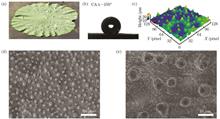
Objective Various bioinspired surfaces about super-wettability have been widely investigated. For example, water droplets move freely on the lotus leaf surface, in an anisotropic way on rice leaf surfaces, and unidirectionally on pitcher surfaces. With the progress of science and technology, the mechanisms for these bioinspired surfaces have been revealed. Importantly, bioinspired surfaces have abroad applications in biological, industrial, micromechanical, and other fields. For example, superhydrophobic surfaces, requiring high roughness and low surface energy, show self-cleaning and anti-icing characteristics. From the view of materials, organic polymer materials have lower surface energy than other materials, showing great potential in developing superhydrophobic surfaces. As a typical polymer material, polyvinylidene fluoride (PVDF) shows excellent flexibility, chemical corrosion resistance, and piezoelectricity. Superhydrophobic PVDF has recently been prepared by various methods, such as hybrid modification and surface chemistry modification. However, these methods require special chemical reagents or complicated equipment. Herein, we designed and fabricated PVDF-based membranes with superhydrophobicity by laser processing technology. After the laser treatment, the laser treated-PVDF (L-PVDF) surface owns microstructures and low surface energy. Therefore, the L-PVDF surface shows superhydrophobicity. This work provides a new method to prepare the PVDF membrane with excellent superhydrophobicity.Methods powders and N, N—dimethylformamide (DMF) solvent are mixed in the ratio of 1 g∶8ml. After ultrasonic treatment for 1h, the PVDF powder is uniformly dispersed. The PVDF@DMF solution is drop-coated on substrates to fabricate PVDF membranes. As for the preparation of L-PVDF surfaces, a continuous semiconductor laser wavelength (λ=450nm, power P=1200mW) is used. After the laser treatment, the L-PVDF surface shows superhydrophobic characteristc. The morphologies of lotus leaf, PVDF, and L-PVDF surfaces are measured by a confocal laser scanning microscope (CLSM) and a scanning electron microscope (SEM). The chemical compositions of the PVDF and L-PVDF are analyzed by X-ray photoelectron spectroscopy (XPS). The surface wettability and wettability stability of the PVDF and L-PVDF are characterized by a static contact angle (CA) measuring system. For the CA measurement, the area of laser treatment is 10mm×10mm, and the processing time is about 3min.Results and Discussion The static CA of water drops on a lotus leaf is ~150°, indicating superhydrophobic characteristic. To explore the mechanism of the superhydrophobic characteristic of water droplets on the lotus leaf surface, we characterized the lotus leaf surface morphology by the CLSM and SEM, respectively. There are microscaled papillae with a diameter of 3--5μm and a height of 5--10μm (Fig. 1). The existence of microscaled papillae can effectively reduce the contact area between water droplets and lotus leaf surfaces, leading to the superhydrophobic effect. Fig. 2 shows the laser processing system and the procedure of laser processing PVDF surface. The SEM images show that there are grooves along the laser scanning path. The distance between grooves is ~100μm, and the width is ~70μm. Moreover, many particles (diameter is ~ 1μm) are observed. The size and shape of particles are similar to the papillae on a lotus leaf (Fig. 3). Besides, XPS is performed to investigate the change of surface composition of PVDF and L-PVDF surface. The C/F atom ratio has significantly changed from 1.2 (PVDF) to 11.5 (L-PVDF), which indicates that the molecular chain of PVDF is destroyed by high laser power, and defluorination may occur (Fig. 4). Compared with the CA of PVDF film (~ 82°), the L-PVDF surface shows hydrophobicity with a CA of ~ 150°(Fig. 5).Conclusions Inspired by the microstructures on the lotus leaf surfaces, a L-PVDF-based superhydrophobic surface has been prepared by a continuous semiconductor laser (λ=450nm, P=1200mW). CLSM and SEM are used to characterize the microstructure of L-PVDF. Grooves and microscaled papillae are induced fabrication by the laser thermal effect. The microstructures on the surface of L-PVDF is similar to that of the lotus leaf surface. Besides, the rough structure reduces the contact area between water droplets and the L-PVDF surface. XPS reveals that the C/F atom ratio on the surface increased from 1.2 (PVDF) to 11.5 (L-PVDF). Therefore, the CA of L-PVDF is mainly dependent on the change of microstructures and composition. The static CA on the L-PVDF surface is ~150°. This work shows the fabrication of superhydrophobic L-PVDF films by laser processing. The laser processing is simple and does not involve chemical reagents. We deem that this method provides a new strategy to prepare a PVDF-based superhydrophobic surface.
Jan. 06, 2021Vol. 48 Issue 2 0202002 (2021)
Misheng Liang, Xin Li, Mengmeng Wang, Yongjiu Yuan, Xiaozhe Chen, Chenyang Xu, and Pei Zuo
Objective As a typical metal microstructure, the metal microgroove structure is widely used in electronics, communications, aerospace, biomedicine, and other fields. With more applications of metal microgrooves in key parts, higher requirements are put forward on the quality and accuracy of microgrooves. For example, in the micro-heat exchange device, the heat transfer pipe with a rectangular cross-section microgroove array structure has better heat transfer performance than other shapes of the microgroove array structure, and the microgrooves with a width less than 50μm show better heat exchange efficiency. In addition, in the field of biomedicine, rectangular microgroove arrays smaller than 50μm have been proven to have better cell orientation effects than rectangular microgroove arrays of 60μm. The precision manufacturing of microgroove structure often requires high machining accuracy (below 100μm), and the machining edge is free of burrs. Besides, the microgroove structure is often processed on many difficult-to-machine materials with high hardness, toughness, and wear resistance. Traditional metal processing methods, such as traditional cutting, electric discharge machining, and electrochemical machining, are often troubled by insufficient precision or difficult material processing when processing high-precision metal microstructures. Ultrafast laser processing has the advantages of high instantaneous power density, low heat-affected zone, and a wide range of materials that can be processed, and it is playing an increasingly important role in precision processing. Ultrafast laser processing has become an essential processing method, especially for difficult-to-process materials such as ceramic materials, superalloys, and superhard materials. However, due to the uneven light field distribution and shielding effect caused by the processing process, the processed micro groove wall is often accompanied by a certain slope, which affects its application performance. Therefore, reducing the groove wall slope while ensuring accuracy is an urgent problem to be solved. In the present study, we adopt an spatial shaping ultrafast laser processing system, based on the principle of beam shaping, built to modulate the Gaussian beam before focusing on a rectangular flat-top light and explore the influence of spatial shaping light on the microgroove structure and reduction of taper.Methods In this study, the laboratory's existing femtosecond laser processing experimental system was used to conduct experimental investigations on nickel-based superalloys. The spatial light modulator (SLM) was used to phase-shape the femtosecond laser, and the Gaussian light was shaped into a rectangular flat-top light and the processing experiment of the microgroove was on the nickel-based superalloy. Then, the surface morphology and three-dimensional morphology of the microgrooves processed by the spatial shaping light were analyzed by scanning electron microscope (SEM) and three-dimensional white light interferometer. In the next step, by adjusting the laser parameters, the processing parameters of the microgroove using the spatial shaping light was studied, and the microgroove and through groove with variable width were processed. In addition, the surface morphology and chemical composition of the microgroove were analyzed by SEM and energy dispersive X-ray spectroscopy (EDX). In addition, the effect of femtosecond laser processing on the oxidation of the microgroove was studied by EDX mapping.Results and Discussion Compared with the Gaussian light, the slope of the microgroove obtained by the spatially shaped light is significantly reduced, and the groove wall profile is straighter. By comparing the effects of different scanning speeds at the same energy, it is found that at a scanning speed of 2000μm/s, as the scanning time increases, the depth of the microgroove gradually increases, and the depth change rate first increases and then decreases. At scanning speeds of 1000μm/s and 500μm/s, the depth of the microgroov gradually increases with the increasing scanning speed, and the depth change rate gradually increases. The analysis shows that with the increase in the scanning speed,the number of pulses deposited in the unit area of the superalloy decreases. After reaching a certain depth, as the processing debris at the bottom of the groove increases, the shielding effect increases, so that the average removed amount of a single pulse is reduced (Fig. 5). As the depth of the microgroove increases, the slope of the groove wall gradually decreases and the minimum slope of the groove wall can reach 1° or less (Fig. 6). In addition, deep grooves with width of 10, 20, and 150μm were processed using spatial shaping light, and the groove wall slope of the deep grooves with a width of 150μm reached 0.63° (Fig. 8 and Fig. 9). The elemental analysis and characterization of the groove wall found that the microgroove wall did not undergo significant oxidation, which should be attributed to the excellent cold working ability of the femtosecond laser (Fig. 10).Conclusions In this study, the strategy of spatially shaped femtosecond laser is adopted and the Gaussian beam is formed into a rectangular flat-top beam by the SLM for metal microgroove processing. Compared with the processing result of the Gaussian beam, the slope of the groove wall fabricated by flat-top beam is significantly reduced. In addition, the method has been used to realize the processing of micro-deep grooves ranging from 10μm to 100μm, indicating that the method has a wide range of processing dimensions. Elemental analysis and morphological observation of the deep groove wall section were carried out. No obvious element changes and laser heat-affected zone were found, indicating the excellent processing ability and great application potential of this method.
Jan. 06, 2021Vol. 48 Issue 2 0202003 (2021)
Mengyao Tian, Pei Zuo, Misheng Liang, Chenyang Xu, Yongjiu Yuan, Xueqiang Zhang, Jianfeng Yan, and Xin Li
Significance Low-dimensional nanomaterials exhibit quantum confinement effects because of their unique size and atomic structures, which enable them to have advanced physical and chemical properties. Therefore, they can be widely applied in nanoelectronics, nanooptics, biochemical sensing, energy devices, and many other fields, indicating their great development potential. Low-dimensional nanomaterials can be divided into zero-, one-, and two-dimensional nanomaterials based on their three-dimensional size. They possess many adjustable parameters, including size, distribution, elemental composition, and functional surface. Therefore, the controllable preparation and property modulation of low-dimensional nanomaterials are essential for ensuring their multifield applications.The current mainstream preparation methods can be categorized as physical and chemical methods depending on the occurrence of chemical reactions. Physical methods primarily include magnetron sputtering, plasma treatment, physical vapor deposition, and electron beam lithography, whereas chemical methods primarily include the hydrothermal method, the template method, electrochemical etching, and liquid phase stripping. Generally, physical methods have complicated processing conditions and high design costs. Through chemical methods, other dangerous chemical reagents can be easily introduced, hindering environmental protection. Therefore, these methods cannot be applied to all materials. Hence, a green, controllable, and material universal method is considerably important for the processing and applications of low-dimensional nanomaterials.Laser processing is a flexible, controllable, and environmentally friendly manufacturing method, which prefers loose processing conditions (no need for high temperature or pressure). Unlike traditional lasers, femtosecond lasers exhibit ultrashort pulse widths, ultrahigh instantaneous power density, and nonlinear processing, resulting in the reduced heat effect, higher processing precision, and the clearer edge of the nanomaterial. They can process almost all types of materials (metals, semiconductors, dielectrics, etc.) and process transparent materials internally. They have unique advantages with respect to the preparation and precision processing of low-dimensional nanomaterials, which are conveniently aimed at targeted position and patterned nanomaterials. Therefore, they are always used to fabricate or process diversified, multiscale, high-precision functional nanomaterials.Progress Zero-dimensional nanoparticles are prepared by femtosecond laser processing mainly based on the system of femtosecond laser liquid ablation. The size, distribution, and crystal form of quantum dots can be modulated by controlling the energy, wavelength, pulse number, and other parameters of femtosecond lasers. In addition, the adjustment of the temporally shaped parameters of femtosecond lasers considerably influences the multilevel photoexfoliation of single-layer quantum dots (Fig. 1) and the photochemical reduction of precursors to prepare amorphous quantum dots (Fig. 3). This is conducive for the preparation of quantum dots with small size, uniform distribution, and high surface activity. Femtosecond lasers can also selectively induce the breakage and rearrangement of chemical bonds, realize the dissociation of chemical reactions and the development of reaction channels in the specified direction (Fig. 2). Thus, the target chemical reaction intermediate products are obtained and the specified functional nanoparticles are achieved. The femtosecond laser preparation of one-dimensional nanowires is mainly achieved via sintering or photoreduction. However, this always involves the introduction of other reagents, necessitating material selection. Wang et al. proposed a method of regulating the spatial parameters of femtosecond lasers to process a gold nanowire with minimum line width of 56 nm which breaks the diffraction limit (Fig. 5). Furthermore, the spatial distribution of one-dimensional nanomaterials is meaningful for their functional applications. Xiong et al. investigated a method for functionalizing the multiwalled carbon nanotubes (MWNTs) to develop a type of two photon polymerization(TPP)-compatible MWNT-thiol-acrylate (MTA) resin, significantly enhancing the electrical and mechanical properties of the three-dimensional micro/nanostructures (Fig. 6). The femtosecond laser processing of two-dimensional films is mainly divided into two categories: modification and ablation. Modification can induce the dissociation of the functional groups on the film surface (Fig. 15), whereas ablation can induce chemical bond rupture to produce highly active defects (Fig. 9). Therefore, the quantum dots prepared using femtosecond lasers exhibit high catalytic activity and are mostly used for electrocatalysis or photoelectrocatalytic hydrogen production. The fabricated nanowires exhibit high resolution and good conductivity and are mostly used for preparing transparent electrodes. The ultrathin films processed using femtosecond lasers contain several surface defect sites, which lead to applications in functional surface preparation, such as superhydrophobic surface, and surface-enhanced Raman scatting(SERS) detection.Conclusion and Prospect In this study, we review the current research status of the preparation and processing of low-dimensional nanomaterials using femtosecond lasers. We introduce the functional quantum dots, nanowires, and two-dimensional thin films prepared using temporally and spatially shaped femtosecond pulsed lasers and their applications in the fields of catalysis, biochemical detection, biocompatibility, and electronic devices. The current technical difficulties associated with the preparation of nanomaterials have been analyzed, and the temporal or spatial parameters of the femtosecond laser affecting the preparation and application performance of nanomaterials have been summarized. Further, the morphological and physical requirements associated with different application fields of nanoparticles have been discussed, and corresponding femtosecond laser processing strategies and future research trends have been proposed.
Jan. 06, 2021Vol. 48 Issue 2 0202004 (2021)
Kaiwen Ding, Cong Wang, Zhi Luo, Huiyong Liang, and Ji’an Duan
Significance As manufacturing quality requirements for functional microstructures increase, ultrafast laser micro/nanomanufacturing has brought new challenges related to high processing efficiency, cross-scale processing, and selective or controllable processing, etc. The limitations of the spatial and temporal energy distribution of traditional ultrafast laser Gaussian beams and processing methods based on single-point focus scanning make it difficult to meet the latest manufacturing accuracy, efficiency, and cross-scale processing requirements. Therefore, researchers focus their attention on manufacturing methods based on ultrafast laser beam shaping.Progress Laser beam shaping can be divided into two types: spatial beam shaping and temporal beam shaping. Spatial beam shaping refers to tailoring the distribution of laser energy in the space domain, whereas, temporal beam shaping refers to changing the distribution of laser energy in the time domain. Compared with a traditional Gaussian beam, a shaped beam has new spatial and temporal energy distribution, which can meet the manufacturing requirements of specific structures or applications.By shaping the spatial profile of an ultrafast laser beam, the fabrication of microstructures with various shapes can be directly realized on exposure to single or multiple laser pulses. Common laser shaping methods include the spatial light modulator method (Figs. 1--3), lens array method (Fig. 4), and beam superposition method. Based on spatial beam shaping, the processing methods such as ultrafast laser direct writing, induction, and deposition can be used for the one-step fabrication of special spatial profile microstructures (Figs. 5 and 6), high aspect ratio microstructures, and optimized processing of microchannels, microstructure arrays (Fig. 7), and laser-induced or -deposited microstructures. By spatial beam shaping, the application range of an ultrafast laser in the manufacturing of functional microstructures can be expanded, the efficiency and precision of which can be improved.Temporal beam shaping transforms a conventional ultrafast pulse into a pulse sequence (Figs. 8 and 9). Each pulse sequence contains several subpulses with a time interval from a femtosecond to a picosecond range. The energy ratio between each subpulse can be derived. Temporal beam shaping can control electronic dynamics during laser-material interactions, which has a wide range of applications in the manufacturing of microchannels (Fig. 10), laser-induced periodic surface structures, nanoparticles (Fig. 11), nanostructures (Fig. 12), and thin films.To further improve the quality and efficiency of ultrafast laser processing, it is necessary to perform the coordinated shaping of ultrafast lasers in the time and space domains. On the one hand, spatial and temporal beam shaping can be performed separately in one optical path by combining double pulses and a Bessel beam (Fig. 13). On the other hand, it is possible to tailor an ultrafast laser in the spatiotemporal domain for coupling shaping by the simultaneous spatial and temporal focusing technology (Fig. 14). Cooperative shaping can considerably improve laser energy deposition efficiency and the three-dimensional symmetry of the intensity distribution of a laser beam focus (Fig. 15).Conclusion and Prospect The ultrafast laser beam shaping technology has the potential to greatly improve the variety, precision, and efficiency of functional microstructure manufacturing. A combination of the ultrafast laser beam shaping technology and microfabrication promotes the efficient and controllable manufacturing of large-area, high-quality functional microstructures, which accelerates the development of commercial scale-forming devices based on the microstructures. However, there are still some challenges with the ultrafast laser beam shaping technology. For example, the laser damage resistance of a shaping device weakens its processing ability, error of the complex shaping system affects its processing accuracy, and interaction mechanism between the shaped ultrafast laser beam and material to be processed is not fully known. These problems and challenges need to be overcome in the future. Facing the need for the miniaturization, integrated design, and large-scale manufacturing of functional microdevices, the ultrafast laser beam shaping manufacturing technology can be highly suitable for high-resolution, cross-scale, three-dimensional, and high-efficiency processing.
Jan. 06, 2021Vol. 48 Issue 2 0202005 (2021)
Rongrong Wang, Weicai Zhang, Feng Jin, Xianzi Dong, Jie Liu, Liangti Qu, and Meiling Zheng
Objective Polyaniline (PANI) has been intensively investigated owing to its low raw-material cost, high electrical conductivity, good environmental stability under ambient conditions, promising chemical, electrical, and optical properties, as well as its unusual doping characteristics. Therefore, PANI has been found to have a wide range of practical applications in many fields, such as supercapacitors, chemical/biological sensor devices, electromechanical actuators, anticorrosion coatings, separation membranes, and battery electrodes. The application basis of PANI is its synthesis. At present, PANI can be synthesized through various chemical/electrochemical approaches; however, the nanostructure uniformity of PANI at the large scale is poor, and the controlled growth of PANI microstructures is difficult in these preparation methods. Furthermore, it is unfavorable to realize the integration and miniaturization of devices. Hence, a synthetic method that is capable of developing regular, controllable, and uniform PANI nanostructures at a micro/nanoscale is required.Two-photon polymerization (TPP) is a photopolymerization method based on the two-photon absorption effect and is an extremely powerful method to achieve real three-dimensional (3D) microdevices. Using femtosecond lasers, which exhibit the characteristics of ultrashort pulse width, ultrahigh precision, and low heat input closely focused into a volume of polymer material, TPP has been employed in the fabrication of diverse micro-objects, such as biochips, micro/nanofluidic devices, and micro/nanoelectromechanical systems. Currently, two-photon polymeric materials are primarily commercial photoresists and hydrogels. These two-photon polymer materials can exhibit strong 3D processing capabilities and better biocompatibility; however, they do not exhibit electrical conductivity. Therefore, we attempt to propose the TPP method to prepare fine and controllable PANI structures and aim to provide new ideas for the preparation of conductive polymers and their wide applicability in sensors, microdetectors, and other micro/nano devices.Methods PANI micro/nanostructures with diverse morphologies were fabricated using the TPP method based on femtosecond lasers. First, using aniline as the monomer and nitric acid as the oxidant, aniline mixed solutions with different molar ratios were prepared. Then, a drop of aniline mixed solution was fixed on the substrate, and the fabricated substrate was placed on the 3D moving stage for TPP processing. After that, a PANI microstructure attached to the glass substrate could be obtained. In addition, the morphology of the PANI microstructure was analyzed through scanning electron microscopy and atomic force microscopy, and the chemical composition of the PANI sample was characterized via Fourier transform infrared spectrometry (FT-IR). Current-voltage curves and resistance values of a single PANI line were tested using a micromanipulated cryogenic probe station-semiconductor characteristic parameter analyzer in a nitrogen atmosphere.Results and Discussions PANI micro/nanowires with different morphologies can be prepared by adjusting the molar ratio of aniline to nitric acid (Fig. 3). The most prominent performance is whether the PANI lines are connected by convex hulls. Under the same laser power and scanning speed, when the molar ratio of aniline to nitric acid is relatively low (samples 1 and 4), it is easier to yield PANI lines with a relatively flat structure. As the concentration of the aniline monomer increased, the PANI lines became denser and thicker. Then, we illustrated the polymerization mechanism of aniline and explained the influence of the aniline concentration on the morphology of PANI lines (Fig. 4). The water-insoluble aniline polymer was synthesized at the water interface. The concentrations of aniline and nitric acid are closely related to the distribution of water-soluble aniline oligomers. When the concentration of aniline was low, the PANI lines with uniform and thin shapes were prepared because all of the aniline monomers in the laser scanning path at the laser focus were converted into aniline oligomers. When the number of aniline monomers in the laser scanning path was extremely large, PANI lines with a convex structure were prepared, which was attributed to the effect on the migration distance of the aniline oligomer with 3D Gaussian distributions. Although samples 1--4 can produce PANI lines, their performances are easily affected by the environment and the stability of the mobile station. To generate PANI with better conductivity and repeatability, we optimized the aniline mixed solution. The performance of the TPP of sample 5 was better than that of other samples (Fig. 5). In addition to the molar ratio of aniline to nitric acid, femtosecond laser power also affected the morphology of PANI lines. Under the high laser power, the PANI lines appear as a more discrete convex hull structure (Fig. 6). With the increasing laser scanning speed, the morphology of the PANI lines became looser, the intermittent situation was intensified, and the width of PANI lines reduced slightly (Fig. 7). Furthermore, FT-IR spectra of PANI were analyzed, which proved that PANI could be successfully prepared by TPP (Fig. 8). The electrical conductivities of the PANI lines were characterized and shown as 5.79×10 -6 S·cm -1 (Fig. 10).Conclusions To directly prepare microstructures of small-scale conductive polymers with controllable shape at one time, the TPP method based on femtosecond laser is proposed, which can realize the precise and controllable preparation of micro/nano-sized PANI. When the ratio of aniline to nitric acid was 1.14∶1, the concentration of aniline was 0.69mol·L -1, the laser power was 14.1mW, and the laser scanning speed was 6μm·s -1. We could obtain the best performing of PANI lines with continuous structure, compact and smooth surface, and good stability. In addition, the FT-IR spectrum characterization of PANI lines demonstrates that PANI is successfully achieved using the TPP method. The electrical conductivity test of PANI shows that PANI is conductive, and its electrical conductivity is 5.79×10 -6 S·cm -1. This study provides a feasible solution for the controllable preparation of conductive polymer microstructures, and the controllable preparation of PANI micro/nanostructures can provide new ideas for the development of conductive polymers in integrated devices.
Jan. 06, 2021Vol. 48 Issue 2 0202006 (2021)
Weicai Zhang, and Meiling Zheng
Significance As is known, biological science research focuses on revealing the essence of life and studying the mystery of growth, development, disease, and aging. To understand all of these, we must begin with understanding the cell behavior. Cell proliferation, differentiation, migration, movement, and other behaviors are closely related to life processes. Thus, understanding the mechanism of these behaviors is of great significance.The surface microstructure of the material can influence the biological behavior of cells, such as inducing cell growth,proliferation and migration, and promoting specific cell functions. While hydrogels are widely used in tissue engineering and regenerative medicine, drug delivery, in vitro cell culture and other fields due to their good biocompatibility and similar composition to extracellular matrix. Therefore, hydrogel micronanometer patterned surfaces and scaffolds prepared by using micro-nano manufacturing technology can provide a more simulated in vivo development environment for the growth of cells and tissues in vitro, which are of great significance for the exploration of the interaction mechanism between cells and cells, between cells and the surrounding environment.Femtosecond laser two-photon polymerization (TPP) is a recently developed micro-nano manufacturing method that can realize the controlled preparation of two-dimensional and three-dimensional (2D/3D) micro-nano structures with high precision morphology. The micro-nano structure of hydrogels prepared by this technology, with both the biocompatibility of hydrogels and the mechanical clues, can more accurately simulate the microenvironment of cell growth in vivo, which has attracted more and more attention in the field of tissue engineering. It is worth mentioning that the resolution of the micro-nano structure fabricated by TPP depends largely on the initiator efficiency. A series of efforts has been made to improve the efficiency of photoinitiators, and significant achievements have been made. However, because most of the traditional initiator molecules are soluble in organic solvents, cytotoxicity originating from organic solvent residue in the micro-nano structure will occur. Therefore, it is particularly important to design and prepare bionontoxic water-soluble two-photon initiators.In the past few years, many advances have been achieved in the preparation of hydrogel micro-nano structures by TPP and its application in tissue engineering. However, there are still many challenges in biosafety initiator design and in vitro cell culture experiments of hydrogel micro-nano structures. Hence, it is essential to summarize the existing relevant researchs and understand the problems in this field in a more comprehensive way, which has guiding significance for the future development direction and implementation methods of this field.Progress In this study, the basic principle of femtosecond laser TPP (Fig.1) and the design and synthesis of a two-photon initiator (Fig.2) are briefly introduced. The research progress of initiators for TPP of hydrogels is mainly introduced, including expanding the length of conjugation system, introducing strong donor/electron acceptor group, adding a coinitiator system to increase the two-photon absorption cross-section, introducing free radical quenching group to reduce the fluorescence quantum yield, and decreasing the cytotoxicity of microstructures by increasing the water solubility of the initiator. Perry et al. designed a series of D-A-π-D-type organic molecules that increase the two-photon absorption cross-section by expanding the conjugate bridge (Fig.3). Belfield et al. synthesized fluorene substituents with different electron-donating and electron-absorbing abilities, which had large transition dipole moment and strong two-photon absorption efficiency, providing new materials for imaging and other two-photon related applications. Xing et al. synthesized new C2v symmetric anthraquinone derivatives by Wittig reaction. These compounds exhibit stronger intramolecular charge transfer bands and lower fluorescence quantum yield (Fig.5). Considering the cytotoxicity of organic solvent residues, the study of water-soluble two-photon initiators has become a hotspot. Bazan's group synthesized a series of organic and water-soluble diphenyl TPA initiators containing dialkyl amino donors by introducing alkyl halide terminal units. On the basis of the principle of host and guest chemistry, the hydrophobic photosensitizer is coated with cyclodextrin and cucurbit urea 7 with large hydrophobic inner cavity size and good water solubility, which is also a simple and environmentally friendly preparation method of a water-soluble two-photon initiator. In our group, Zheng et al. have proposed designing and synthesizing a series of carbazole-based ionic two-photon initiators and further improving its two-photon absorption property by using host-guest chemistry. By varying the chemical microenvironment during polymerization, the TPP of precise configuration in an aqueous phase can be realized, which is important to avoid the cytotoxicity usually caused by conventional two-photon initiators (Fig.7). These studies are the scientific basis of the fabrication of 3D biocompatible hydrogels' micro-nano structures and are the necessary conditions for better simulating the biological microenvironment in vitro. Then, the micro-nano structure of hydrogel made using TPP and the application of these structures in tissue engineering are introduced. Furthermore, the existing problems and the future development trend in the application of biocompatible hydrogel microstructures were summarized and prospected.Conclusion and Prospect In past decades, conventional TPP initiators have made significant progress. Researchers have made much effort to develop two-photon initiators with high initiation efficiency and low polymerization threshold. A series of water-soluble two-photon photoinitiators without cytotoxicity have been designed, considering biosafety, to improve the biocompatibility of the 3D microstructure of hydrogels while ensuring the two-photon absorption characteristics. At present, although the research and development of water-soluble two-photon photoinitiators have been achieved, there are still some shortcomings, such as understanding the polymerization mechanism and low initiation efficiency, which still need to be further studied. Also, the size of the current TPP hydrogel microstructure is small (nanometer level), unable to meet the needs of a large amount of cell culture and tissue growth in vitro, so the rapid preparation of large hydrogel microstructure with TPP will be an important research focus in the future.
Jan. 06, 2021Vol. 48 Issue 2 0202007 (2021)
Cai Mingyong, Jiang Guochen, and Zhong Minlin
Significance It is well known that energy, material, and information have been regarded as the three cornerstones of human civilization and social development. The exploitation and utilization of energy by human beings has continued through human evolution without interruption. Fossil fuels, including coal, oil, and natural gas, have promoted tremendous social change and brought inestimable value to human beings. Traditional fossil fuels are non-renewable energy sources with limited reserves in the earth''s crust. Excessive exploitation without replacement or alternative energy sources will inevitably lead to fossil fuel depletion. Due to increasing environmental pollution, humans begin to realize environmental hazards caused by the excessive use of fossil fuels, such as global warming, acid rain, and particulate matters. With respect to severe energy and environmental crises, it is imperative to develop green and clean energy technologies to reduce the use of increasingly exhausted fossil fuels and achieve environmentally-friendly and sustainable social developments.Hydrogen, as a renewable energy carrier, has attracted significant attention due to the following four reasons. First, hydrogen is a clean and low-carbon energy carrier and its reaction product is only water with no carbon dioxide emissions. Second, hydrogen has a high calorific value, about three times higher than fossil fuels. Third, hydrogen is widely used in electricity, construction, transportation, and industrial fields. It can be used as a raw material for the steel, metallurgical and chemical industries and as a fuel in fuel cells. Fourth, hydrogen is earth-abundant, which can originate from fossil fuel reforming, water splitting, and by-products of the chlor-alkali industry. Many governments around the world are committed to developing hydrogen energy and arranging relevant industrial chains. The International Renewable Energy Agency pointed out that hydrogen can build a connection among electricity, construction, industry, and transportation to achieve deep decarbonization.Developing various technologies for hydrogen production is important in developing hydrogen energy and the hydrogen economy. Nowadays, there are three main pathways for hydrogen production, namely, methane-steam reforming, coal gasification, and electrocatalytic water splitting. Though the first two pathways account for about 95% of hydrogen production, they still rely on fossil fuels and emit large amounts of carbon dioxide, which violates the goal of developing hydrogen energy. In contrast, electrocatalytic water splitting does not lead to carbon emissions and is a green and sustainable hydrogen production technology. However, electrocatalytic water splitting has shortcomings of excessive energy consumption and high cost, which restricts its large-scale application. Electrocatalytic water splitting contains a cathodic hydrogen evolution reaction (HER) and an anodic oxygen evolution reaction (OER), both which need efficient electrocatalysts to overcome the high reaction barrier. Therefore, how to improve electrocatalytic performance and reduce electrolytic overpotential are keys in realizing large-scale applications of electrocatalytic water splitting.Over the past few years, various methods have been developed to prepare electrocatalysts for electrocatalytic water splitting, mainly including the hydrothermal/solvothermal method, sol-gel method, electrochemical deposition, chemical bath deposition, chemical vapor deposition, and physical vapor deposition. Specifically, lasers have become an effective tool to prepare catalysts for electrocatalytic water splitting with advantages of being efficient, flexible, contactless, and highly controllable. Many corresponding advances have been achieved, but they still face a series of challenges in terms of industrial feasibility and performance improvement. Hence, it is important and necessary to summarize the existing research to guide the future development of this field more rationally.Progress Preparation methods of electrocatalysts for electrocatalytic water splitting based on lasers and their catalytic performances have been summarized. First, the implementation process of electrocatalytic water splitting, evaluation parameters, classification, and preparation methods of electrocatalysts are introduced. The evaluation parameters include overpotential, Tafel slope, stability, Faraday efficiency, and turnover frequency. Then, the catalytic performances of electrocatalysts prepared by laser are comprehensively summarized according to previously reported studies. Subsequently, powder catalysts by laser in liquid and self-supported catalytic electrodes with micro-nano structures by laser are elaborated. Considering the interaction mechanism, the preparation process of powder catalysts by laser can be divided into laser irradiation in liquid and laser ablation in liquid. Haimei Zheng''s research group from University of California, Berkeley, has pioneered laser irradiation in liquid. Xiwen Du''s research group from Tianjin University has engaged in plenty of systematic studies on laser ablation in liquid. Based on the preparation method, the preparation process of self-supported catalytic electrodes with micro-nano structures by laser can be divided into laser direct preparation and laser hybrid with other chemical synthesis methods. Currently, studies of self-supported catalytic electrodes by laser are limited and incomprehensive. In the end, the problems faced and ongoing research trends in this field are discussed, including the type of laser, the characterization and theoretical calculation of catalysts, the design of bifunctional catalysts, and the performance evaluations at industrial conditions.Conclusion and Prospect Lasers are gradually becoming a popular tool to prepare various functional materials. In summary, the preparation of micro-nano catalysts for electrocatalytic water splitting by laser still needs in-depth and detailed exploration to promote the development of this hydrogen production technology in academic and engineering aspects.
Feb. 01, 2021Vol. 48 Issue 2 202008 (2021)
Rui Pan, Hongjun Zhang, and Minlin Zhong
Objective Ice accretion and its subsequent removal can be great threats to aircrafts, power lines, wind turbines, marine structures, and even the pipes of air conditioners or refrigerators, which may lead to serious life safety problems and enormous economic loss. Traditional deicing methods, such as mechanical vibration deicing, electro-thermally deicing, or chemical fluid deicing are usually energy-intensive and/or environmentally unfavorable. Alternatively, emerging passive anti-icing (for prevention or delay of ice accumulation) and icephobic (for easy removal of ice) surfaces have been widely studied. Among them, superhydrophobic surfaces are promising candidates due to their extreme high-water repellency. However, superhydrophobic-based ice-resistant surfaces are facing three possible problems, including low humidity tolerance, relatively high ice adhesion strength which needs to be further reduced and poor deicing mechanical durability. In the present study, we report a novel kind of triple-scale micro/nano-structured superhydrophobic surface with comprehensive anti-icing and icephobic properties via ultrafast laser hybrid fabrication. This type of superhydrophobic surface exhibits excellent Cassie state stability, high humidity resistance, and good deicing durability. We hope that our basic strategy and findings can be helpful for the design of new robust ice-resistant superhydrophobic surfaces and the relationships between superhydrophobicity and ice resistance.Methods Copper and aluminum alloys have been employed in the present study. First, the triple-scale micro/nano structures, composed of microcone arrays covered with densely grown nanograsses and dispersedly distributed micro and/or submicron flowers, were fabricated on the surfaces via a hybrid method combining ultrafast laser ablation and chemical oxidation. Then, the resultant surfaces were chemically modified by fluoride to induce superhydrophobicity. After that, contact angle and sliding angle of the surfaces were tested on a video-based optical contact angle measuring device. Then, the morphologies and chemical compositions of the textured surfaces were analyzed by scanning electron microscopy and X-ray diffraction. The effects of chemical oxidation time on the morphology and superhydrophobicity of the prepared surfaces were studied. In the next step, condensation observations and icing delay experiments were performed on the optimized superhydrophobic surfaces to assess their anti-icing performance. Furthermore, ice adhesion strength and icing-deicing cycles were also measured and performed for the prepared superhydrophobic surfaces to characterize their icephobic properties.Results and Discussions The prepared triple-scale micro/nano-structured surface possesses excellent superhydrophobicity with a contact angle greater than 160° and a sliding angle less than 1° (Fig. 3). With increasing oxidation time, the nanostructures formed on the microcone arrays on the surfaces evolved from nanorods to nanograsses via hydrolysis (Figs. 4 and 5). Overall, the resultant contact angle increases and the sliding angle decreases with increasing oxidation time (Table 3). The anti-icing function study shows that the optimized superhydrophobic surface is featured with hierarchical condensation and coalescence-induced jumping of the condensed droplets under condensation and freezing conditions due to its low surface adhesion (Figs. 6 and 7). Since the air pockets trapped in the surface structures perform as a thermal barrier layer, the prepared superhydrophobic surface exhibits good icing delay performance with an icing delaying time of 52 min 39 s (Fig. 8). The icephobicity study of the prepared superhydrophobic surfaces shows that the ice adhesion strength of the superhydrophobic surface can be as low as 6 kPa, which is 40 times lower than that of the original aluminum alloy surface (Fig. 10). In addition, after 10 repeated icing-deicing cycles, the ice adhesion strength of the superhydrophobic surfaces are still no more than 20 kPa (Fig. 10), demonstrating decent deicing robustness.Conclusions In the present study, a novel kind of triple-scale micro/nano-structured superhydrophobic surface, composed of periodical microcone arrays covered with densely grown nanograsses and dispersedly distributed micro/submicro-flowers, were successfully fabricated via ultrafast laser hybrid method. After chemical modification, such a surface possesses excellent superhydrophobicity with a contact angle greater than 160° and a sliding angle less than 1°. The surface morphology evolution shows that the superhydrophobicity of the prepared surface is determined by the surface roughness and hierarchical level. The observed hierarchical condensation phenomenon on the prepared superhydrophobic surface ensures the Cassie state stability of the primary condensed droplets even under high humidity and the condensed droplets can slide off the surface before freezing due to low surface adhesion, thus enabling the prepared superhydrophobic surface with great anti-icing performance. The ice adhesion strength of the superhydrophobic surface can be as low as 6 kPa, which is very competitive even compared with the interfacial slippage surfaces and the low interfacial toughness surfaces (the reported ice adhesion strength can be as low as 5 kPa), indicating that superhydrophobic-based icephobic surfaces can also exhibit ultralow ice adhesion. Our study shows that such kinds of triple-scale micro/nano-structured superhydrophobic surfaces with comprehensive anti-icing and icephobic properties can be obtained through rational surface design, which couples multi-scale micro/nano roughnesses and hierarchical levels.
Jan. 06, 2021Vol. 48 Issue 2 0202009 (2021)
Chunhe Li, Zhuochen Ma, Xinyu Hu, Lin Zhu, Bing Han, and Yonglai Zhang
Significance Microfluidic chips incorporate basic operation units such as sample preparation, reaction, separation, and detection on a microchip, revealing great potential in the chemical and biological analysis. Compared with the traditional macroscopic large-volume systems, microfluidic chips feature the advantages of high efficiency, low loss, high safety factor, and high sensitivity. As a high-throughput micro-scale analysis device, the microfluidic chip system has shown significant potential in the highly sensitive detection of various chemical and biological molecules. So far, several detection methods such as ultraviolet-visible absorption, plasma atomic emission spectrometry, inductive coupling, mass spectrometry, chemiluminescence, laser-induced fluorescence, thermal lens microscopy, and biosensors, have been successfully applied to microfluidic systems. Among them, the surface enhanced Raman scattering (SERS) method as a unique detection technology was also introduced to the detection of microfluidic chips and rapidly developed in the past decade. Because SERS is a fingerprint feature map with rich spectral lines, it has high sensitivity, fast speed, and non-contact. Combined with the characteristics of the microfluidic chip, the SERS detection method shows several unique advantages: the laser spot is small and can be directly focused on the tiny channel of the microfluidic chip; the high sensitivity is especially suitable for the requirement of a small amount of reagents in the microfluidic chip; it has no direct contact with the reaction reagents, and it has no interference to the reaction system; with fingerprint spectral characteristics, it can be used to analyze and identify the mixture in the reaction system.Progress In this review, we will discuss and study the development of SERS microfluidic chips from two parts. The first part is the preparation of microfluidic chip channels and integrated SERS substrates. The second one is the application of SERS integrated microfluidic chips. Figure 1 shows the overall discussion ideas of this article. For the preparation of microfluidic channels, two preparation methods are mainly introduced: wet etching assisted femtosecond laser direct writing and soft lithography. The first method is more complicated and requires multiple processing steps, but the preparation accuracy and detection results are relatively ideal. As a digital processing method, there is no need to replace different templates, especially for the unique advantages of the preparation of the three-dimensional channel. The second method is relatively simple, but two problems need to be addressed. The first is to control the hardness of the PDMS, as the excessive softness will affect the fluidity of the liquid in the channel; the second is to optimize the channel structure to make the device have higher repeatability and stability. The preparation and integration of SERS substrates include the following four methods: colloidal self-assembly, femtosecond laser direct writing (FsLDW) induced metal ion reduction, dual-beam interference, and light scribing. These methods have their pros and cons. The cost of the colloidal self-assembly method is relatively low, the method is relatively simple, but its dispersion uniformity is poor. Femtosecond laser direct writing has obvious advantages in processing accuracy, but the processing time is too long and it is thorny for large-area preparation of the substrate. Dual-beam interference has successfully solved the problem of slow processing speed, but the complexity of the processing pattern and topography of the substrate need to be strengthened. Light scribing meets the requirements of rapid processing and patterned preparation, but there is room for further enhancement in preparation accuracy. In addition to the above-mentioned preparation methods, there are also many methods to prepare SERS microfluidic chips, such as two-photon polymerization, AAO template method for preparing nanostructures, and built-in optical fiber SERS probes. We analyzed the advantages and disadvantages of various methods and summarized the detailed data of the typical research work in this part, and compared them in Table 1. In terms of application, it focuses on the analysis and detection of harmful substances, in-situ monitoring of chemical reactions, biomolecular detection and immunoassay, and cell metabolite detection and analysis of SERS microfluidic chip. We summarized the typical research work of this part in Table 2 and proved that this technology has broad applications in many aspects. However, behind the rapid development of technology, there are still some problems. For example, in biological detection, due to the significant differences in the pH tolerance, life span and size of different types of cells, each chip can only detect corresponding one or several kinds of cells. The current preparation methods of such SERS substrates are mostly colloidal self-assembly methods, which is a huge challenge for the popularization and application of SERS microfluidic chips in this direction.Conclusion and Prospect With the support of the above content, promoting the development of portable applications of SERS detection microfluidic chips has become a major challenge. To realize the portability of the microfluidic SERS detection system, current research focuses mainly on the transition from active liquid driving to liquid self-driving. For liquid self-driving, the capillary effect is mainly used to replace equipment such as injection pumps that need to add liquid to the chip multiple times. By using this technology, we can reduce the use of pumps and even replace the role of pumps. In addition, with the rapid development of a new generation of manufacturing technology, the production efficiency, accuracy, and stability of microfluidic chips will be significantly improved, and people will gradually solve the problems of long time and high cost in the manufacturing process. With the help of new technologies, microfluidic technology will achieve more functions, and it will be more integrated with SERS detection, various performance indicators will be more excellent, and various devices will be highly integrated. We look forward to the continuous development of this technology and its early use, making contributions to people's daily life, industrial production, and biological testing.
Jan. 06, 2021Vol. 48 Issue 2 0202010 (2021)
Zhizhen Jiao, Jichao Li, Zhaodi Chen, Dongdong Han, and Yonglai Zhang
Significance The interaction between light and matter makes our world colorful, which includes absorption, reflection, scattering, transmission, diffraction, and interference. The antireflection (AR) characteristics of material surfaces are beneficial to improve the coupling of specific incident electromagnetic waves and the ability to distinguish particular electromagnetic signals. The AR characteristics are also helpful to shield and eliminate specific interference signals. Reducing the incident light reflection on material surfaces and improving reflection and transmission are vital to the utilization of solar energy, flat panel displays, infrared imaging, surface Raman enhancement, optoelectronic devices, military stealth, and aerospace technologies. Therefore, it is crucial to perform an effective light management and improve the performance of optical devices.There exist many AR surface (ARS) fabrication methods, such as sol-gel, chemical vapor deposition, nanoimprinting, wet etching, dry etching, and laser processing. Among them, laser processing has attracted much attention owing to its advantages of high efficiency, programmability, high processing resolution, noncontact processing, high flexibility, and environment-friendly operation. Moreover, it is suitable for almost all materials (e.g., silicon-based materials, polymers, metal films, and carbon-based materials). Furthermore, femtosecond laser processing is a cold working process, which is highly suitable for complex and precise surface structure processing. Therefore, laser processing technologies stand out in the field of ARS preparation. To further improve the processing efficiency, multibeam parallel processing, or laser processing technology combined with other preparation methods such as wet etching or dry etching can be used. Above all, laser processing is a powerful tool for preparing AR structures on any material surfaces.This review summarizes the latest progress in laser processing of ARSs , elaborates on the principle of AR and the selection of AR materials, and summarizes the current applications of ARSs in various fields, including solar cells, LEDs/OLEDs, photodetectors, and solar-driven water evaporators. Many excellent reports have described the preparation of ARSs; however, there are still some challenges in their large-scale industrial production and practical application. Therefore, summarizing the existing research is crucial to guide the future development of laser processing technologies.Progress First, we summarize the principles of AR in detail using the Fresnel equation and elaborate on various structure sizes and light effects ( Fig. 1). Then, according to previous reports, we summarize the advantages and disadvantages of various ARS preparation methods, structures and morphologies, and the scope of laser processing technologies ( Table 1). In addition, we introduce how to effectively improve the efficiency of laser processing for preparing ARSs. For silicon-and silicon-oxide-based materials, Papadopoulos's research group has used circularly polarized ultrashort laser pulses to induce a subwavelength nanopillar structure on fused quartz, realizing a useful ARS with a full angle and broad spectral range ( Fig. 2). For metal-based materials, Fan's research group has successfully prepared an AR micro-nanohybrid structure on a copper surface using a laser direct writing strategy controlled by pulse injection ( Fig. 3). For polymer matrices, Leem's research group has prepared a polydimethylsiloxane (PDMS)AR layer using a moth-eye AR structure on a glass substrate using double-beam interference combined with dry etching and transfer technology ( Fig. 4). Moreover, silicon and silicon oxide, metals, and polymer-based materials are summarized comprehensively ( Table 2). ARS applications such as solar cells ( Fig. 5), OLEDs ( Fig. 6), photodetectors ( Fig. 7), solar-driven water evaporators ( Fig. 8), and multifunctional bionic surfaces are discussed in detail. Finally, the existing problems in ARS preparation are discussed, with a focus on the processing efficiency, problems in practical applications, and the challenges in industrial production.Conclusion and Prospect ARSs based on micro-nanostructures display excellent characteristics such as wide angle, broad spectra, and polarization insensitivity, and have been widely used in solar cells, LEDs/OLEDs, photodetectors, and photothermal conversion. As the ARS preparation technology continues to develop, laser processing stands out owing to its high processing resolution, high efficiency, and programmable design. This review introduces the ARS technologies, including surfaces and morphologies, selection of AR materials, and the applications of ARSs, especially the progress in recent years. Although there are still some unresolved problems in the preparation of ARSs by laser processing, we firmly believe that through further in-depth research and structural optimization of existing ARSs, a much higher-quality ARS can be prepared. We expect these advances will bring development to many areas such as the photovoltaic industry, military, and aerospace industry as well as LEDs, and thus promote the development of renewable energy and national economy.
Jan. 06, 2021Vol. 48 Issue 2 0202011 (2021)
Yansheng Yao, Jianping Tang, Yachao Zhang, Yanlei Hu, and Dong Wu
Significance The scientific and technological community has shown an increasing interest in amorphous alloy materials because of their excellent properties, such as high strength, high hardness, and good corrosion resistance. With the development of high-end equipment manufacturing and the increasing demand for principal devices, applying laser-manufacturing technology to form bulk amorphous alloy components, amorphous strengthening, and micro-machining of the material surface has received increasing attention. For decades, people have studied the forming and processing technology of bulk amorphous alloys. Copper mold casting and thermoplastic forming technology have been widely used to form amorphous parts. The copper mold casting method has high forming efficiency, but the complexity and size of the amorphous components are limited. Thermoplastic forming technology has high forming precision and can form amorphous components with a surface micro-nano structure, but the size is still limited, and the powder composition is strictly required. Regarding machining, some methods exist, such as diamond turning and micro-EDM, but they easily crystallize amorphous materials in the machining process. With the development of critical special equipment and complex amorphous components, traditional manufacturing methods are difficult to meet the requirements; therefore, there is an urge and necessity to explore new technologies for the efficient forming and processing of amorphous alloys.Progress Selective laser melting (SLM) technology can fabricate bulk amorphous alloys without size limitation to form a complex structure of precision pure amorphous devices and increase the heating and cooling rate in the molten pool by changing process parameters. However, no universal rule in parameter selection exists, and there are few studies on crystallization and other mechanisms, which must be further studied. Laser welding technology splices small-size amorphous alloys together to form large-size amorphous alloys without changing the amorphous characteristics, with the advantages of a simple process, high production efficiency, and high application value. However, the heat-affected zone easily crystallizes at low temperatures and slow cooling stages; therefore, simulation and theoretical analysis must be combined to predict whether crystallization can be used to obtain the process parameters of amorphous welding. The technologies of laser amorphization and laser-cladding amorphous coating are surface-strengthening methods for different degrees of corrosion resistance, wear-resistance, and other extreme conditions. It is easy to operate and has several applications. The amorphous layer obtained by laser surface amorphization technology is thin, and the properties of the amorphous layer significantly depend on the material composition and properties of the substrate. The laser-cladding amorphous coating makes up for the inherent defects of laser surface amorphization. However, because of the influence of the growth of the substrate epitaxial layer and the uneven flow of the melt, it is challenging to obtain pure amorphous coating, and the coexistent form and formation mechanism of the amorphous and crystal phases in the coating are unclear. The synergistic effect of the crystalline and amorphous phases on the properties of the coating must be studied. The processing of amorphous alloys by laser ablation, especially femtosecond laser processing, has the advantages of a minimal heat-affected zone and accurate ablation threshold that can realize high precision and amorphous processing of amorphous alloys. However, the laser process parameters' effect on the efficient machining of various bulk amorphous alloys and the fabrication of surface micro-nano structures must be further studied. Currently, most of the significant scientific and theoretical issues of amorphous alloy laser-manufacturing technology are unclear, and many scholars predominantly improve the forming and processing quality of amorphous alloys from the aspect of process exploration. Thus, the excellent properties of amorphous alloys are applied in related technical fields.Conclusion and Prospect With the development of high-end equipment manufacturing and precision devices and amorphous alloy systems with special properties, the research and application of laser-manufacturing technology of amorphous alloy materials in various systems will be pushed to a new height. Therefore, the formation and processing of amorphous alloys require continuous process testing to obtain optimal components and deep research into the principal mechanism research in the manufacturing process of amorphous alloys. Combined with simulation and theoretical analysis, the optimal machining parameters are obtained. Laser augmentation manufacturing and laser welding can realize the formation of large-size amorphous alloys, which can meet the applications of high-performance and large-size amorphous devices. However, in most industrial applications, using bulk large-size amorphous alloys increases manufacturing costs. Amorphous layers were obtained on the surface of common metal materials using laser surface amorphization and cladding technology. The excellent properties of amorphous alloys are grafted onto the surface of common metal materials, which can reduce manufacturing costs and improve the surface properties of metal materials. Laser ablation-processing technology can change the shape of bulk amorphous alloys, which makes amorphous alloy applied in various fields and occasions in various forms of devices, especially in precision instruments and machinery, have a broad application prospect. Laser-manufacturing technology of amorphous alloy materials has significant potential in aerospace, precision instrument production, biomedicine, and other fields, but the application of technology in these fields is still in its infancy, and further research is urgently needed.
Jan. 06, 2021Vol. 48 Issue 2 0202012 (2021)
Congcong Bai, Junhao Zhang, Chang Gao, Xuting Jin, Xin Li, Wei Xiong, Jianfeng Yan, Zhipan Zhang, Yang Zhao, and Liangti Qu
Significance Emerging portable wearable electronic devices require high-performance and integrable micropower sources. Micro-supercapacitors with high power density, rapid charge and discharge, and long life cycles have received widespread attention. Differing from the traditional sandwich structure, planar micro-supercapacitors do not require separators because their electrodes are on the same plane with certain physical distance, including parallel line, interdigital, and coil types, which significantly reduce the interface contact resistance and improve the electrochemical performance of the device. In addition, the ion transmission path of planar micro-supercapacitors would remain constant as the electrode load increases due to the unique vertical opposite cross-section electrode structure. This could increase energy density without losing power density. The miniaturized planar structure is considered highly compatible with microelectronic systems that can be integrated into other circuits as power supply units to provide effective peak power within a short time.To date, various planar micro-supercapacitor construction methods have been developed, such as oxidation etching, printing, and photolithography technologies. However, some challenges remain. Oxidation etching technology involves multiple steps and complex operations, which, at minimum, requires a template to construct metal current collectors while removing the excess active material. Low-cost inkjet printing can be used to construct the current collector in a non-contact manner; however, the preparation process of the printable ink is complicated. Although photolithography technology is often used to prepare the planar electrode arrays of micro-supercapacitors, the post-processing procedures are cumbersome, which limits its application in the integrated manufacturing of microdevices. Compared with the above preparation methods, laser processing technology, which does not require a template and features high processing speed and nanometer spatial resolution, is a promising and efficient tool. Specifically, the designated electrode patterns can be precisely constructed using laser processing technologies on demand. For example, ultrafast lasers, which have instantaneous high energy with low thermal impact and negligible working area deformation, can also accurately control and fabricate microelectrodes in a short time. To improve overall performance, the physical and chemical properties, such as modification, doping, and electrode conductivity, can also be controlled in situ and regulated by adjusting laser parameters. Laser process technology has become increasingly important in the development of microdevices. Therefore, there is a great need to summarize the research progress of laser processing for micro-supercapacitors to provide references for the future design and preparation of advanced micro-energy storage devices.Progress Due to its unique advantages, laser technology is widely used in the physical processing of electrode patterns and the modification of electrode materials for micro-supercapacitors. Laser technology can be employed to realize in situ fabrication or adjustment of micro- and nanostructures in electrodes and composite electrodes with pseudo capacitance and electric double layer capacitance. Thus, laser technology is considered an effective and convenient manufacturing strategy for micro-supercapacitors. More importantly, the capabilities of laser technology to realize the precise size and shape of microelectrodes as well as the possible for large-scale integration of various circuits provide a variety of potential application scenarios for micro-supercapacitors. In the physical construction of patterns, researchers have been able to effectively control the distance between adjacent electrodes by adjusting the processing accuracy of the laser, which can shorten the ion transmission path between two electrodes, thereby improving device performance. For example, adjustable finger-shaped microelectrodes were obtained simultaneously on the upper and lower surfaces of graphene oxide (GO) film, in part, to the flexible controllability of the laser. Surface capacitance could be further improved by connecting devices in series outside the plane. In addition, laser technology has also been used to realize a microelectrode current collector or mask, which usually acts as a substrate or template to realize microelectrodes through simple template imprinting, electrodeposition, and other methods. Laser processing technology has been deployed to facilitate efficient, large-scale production of miniature energy storage devices whereby hundreds of miniature devices can be produced in a short time. The advantages of lasers are also reflected in the fast and effective integration of different circuit components to support low-loss energy conversion.Research on electrode modification revealed that adjusting laser scanning parameters, such as laser power and scanning speed, affected the conductivity of some specific electrodes to a certain extent, such as the use of laser photothermal reduction of GO materials. In addition, doping and modifying nanoparticles or atoms in microelectrodes could also be performed in situ using laser direct writing technology. In this regard, various composite electrodes and heteroatom doped electrodes were obtained by laser processing the raw material containing functional components. For example, boron-doped electrode materials were successfully prepared by laser processing a PI sheet containing boron elements. Moreover, the heteroatom doping process has also been achieved by placing the electrode material in a special environment for laser processing. For example, nitrogen doping of GO material was prepared in the presence of ammonia by irradiating the GO solution with a laser.Conclusion and Prospect Currently, the primary role of lasers in the construction of miniature supercapacitors is physical marking and electrode modification. Due to their unique advantages, lasers have gradually become a popular tool for preparing micro-supercapacitors. However, this process still requires in-depth and detailed exploration to promote the comprehensive application of this processing technology in miniature energy storage devices.
Jan. 07, 2021Vol. 48 Issue 2 0202013 (2021)
Changxiang Shao, Yang Zhao, Nan Chen, Hongwei Zhu, Lei Wang, Hongbo Sun, and Liangti Qu
Significance The emerging technologies such as the Internet of Things and wearable technology in recent decades have brought great changes and convenience with better healthcare and manufacturing and higher safety, security, and efficiency for the whole society. As an essential important link in these systems, sensors provide key value proposition and play a pivotal role. Take wearable electronics as examples , the market value of wearable technology has doubled in the past five years. Sensors have provided core functions for many different products during the development of wearable electronics, and they will continue to play a key role in future generation of products. For example, smartwatches and skin patches are built based on the fitness tracking and daily activity data, and are used for medical measurement. Virtual, augmented, and mixed reality devices rely on a set of sensors (e.g. inertial measurement unit, depth induction, force/pressure sensors) to enable users to interact with the content and environment. Moreover, the transition from traditional human-computer interaction to a natural user interface will also depend on further advances in sensors. Other products in different areas, such as autonomous vehicles, air detector, and smart clothing, are similar and depend on a set of core sensors that can interact with the body or the surrounding environment. Some of these sensor systems have been gradually commercialized and expanded to more industrial, agricultural, military, environmental, and safety applications. In particular, the COVID-19 pandemic in 2020 has also brought increased attention to sensors owing to their promising applications in tracking early onset and potential virus contacts, and remote patient monitoring of isolated patients. In short, the sensor remains a fundamental component of the entire product line, which has been required to be thinner, lighter, smaller, more flexible, and sensitive in the new application systems.Based on the important role of sensors, many preparation methods such as vapor deposition, lithography, nano-imprint lithography as well as printing have been developed. Each technology has its unique advantages and adapts to different scenarios. At the same time, their disadvantages that cannot be ignored also need to be addressed. For instance, chemical and physical vapor deposition methods, including thermal evaporation, vacuum evaporation, magnetron sputtering, and molecular beam epitaxy, can produce high-quality materials and devices with good performance, but these technologies usually require expensive equipment and specific operating environment. Moreover, it is difficult for these techniques to be compatible with flexible substrates and realize low-cost industrialized mass production. In addition, photolithography and nano-imprint lithography are suitable for precision device fabrication. However, they often face the challenges of low processing efficiency, low output, high cost due to the complex processing process, high design cost of mask, and long processing cycle. In comparison, printing is a very attractive technology for low-cost large scale production. But in most cases, the presence of mask limits the precision and resolution of the prepared micro/nano-sized devices. Therefore, with the increasing demand for flexible, wearable, miniaturized, precise, integrated, and customized sensors, the new processing method with higher precision and more flexibility manners is needed to achieve controllable preparation.To meet the developmental requirements of sensors, various processing techniques mentioned above are utilized to optimize and improve the sensor mainly from the aspects of the electrode, sensing material, and whole device. In recent decade, laser micro-nano fabrication has been gradually developed and popular in the field of manufacturing. The laser micro-nano fabrication changes the material state and property through the laser-material interaction and realizes the well-control of shape and property across scales. With the advantages of large processing speed, high precision, strong controllability, easy integration, and high compatibility with materials, the sensor fabricated by laser has ushered in a new development in structure regulation and performance optimization. However, it still faces challenges and difficulties in mass production and efficiency promotion in practical applications.Progress The laser processing technologies for the fabrication of sensors and sensing systems of different stimulus sources are summarized ( Fig. 2). Firstly, three laser processing modes widely used in sensor production including laser induced heating, reaction, and delamination are introduced. The convenience and advantages of laser processing compared with those of the traditional processing technology can be clearly understood in the section of laser processing modes ( Fig. 3). Then, based on the existing research results, the sensor systems prepared by laser are classified into ultraviolet, gas, humidity, temperature, strain/stress, biology, and environmental monitoring sensors. It is easily found that the advantages of laser micro-nano fabrication are mainly reflected in the following three aspects. 1) Laser micro-nano fabrication has broadened the preparation approaches of electrodes and sensing materials. It can realize in-situ or non-in-situ preparation of conductive electrodes and sensing materials by laser reduction, sintering, annealing, ablation, pulse deposition, laser induced carbonization, and hydrothermal reaction as well as other specific laser processing technologies, which provide alternative strategies for material preparation. 2) Laser micro-nano fabrication simplifies the assembly process of the whole device. The laser direct writing technology can realize in situ selective process in specific areas or specific materials, leading to great convenience for device construction. Moreover, the whole sensor on flexible substrates can even be prepared by one-step laser fabrication through digital design. 3) Laser micro-nano fabrication contributes to promote sensor performance. Sensing material, as a key part of a single sensor, can be modified and regulated by laser processing, thus providing the possibility of performance optimization. With these optimizations and improvements, the sensors become softer, smaller, and more customized and have higher integration. Finally, we also analyze the problems existing in sensors fabricated by laser micro-nano fabrication, such as insufficient researches on laser-material interaction, limited processing accuracy and efficiency enhancement, and low level of device integration.Conclusions and Prospect Laser micro-nano fabrication has gradually become a common and popular technology for sensing system preparation and integration. To sum up, the sensor fabricated by laser still needs in-depth and detailed exploration to promote the development of commercialization and industrialization of the sensor.
Jan. 06, 2021Vol. 48 Issue 2 0202014 (2021)
Yutong Ran, Wenduo Chen, and Hongwei Zhu
Significance With the rapid development of society, the traditional fossil energy is increasingly exhausted, and the problems of energy shortage and environmental pollution are becoming more and more serious. Human demand for clean and efficient energy is becoming more and more urgent. Vigorously developing new energy has become the core issue of nowadays society. Now, a variety of new and sustainable energy sources are emerging, such as wind energy, solar energy, biomass energy, and water energy. Thermal power generation is one of the hot new energy sources. The thermoelectric conversion efficiency is directly proportional to the thermoelectric merit of thermoelectric materials. Tin selenide (SnSe) has a thermoelectric merit value of 2.6 (923K), which is one of the materials with the highest thermoelectric conversion efficiency and is widely used in many fields. However, the preparation method needs to be improved, and the thermoelectric properties of media and low temperature properties are not excellent. Therefore, the research progress of SnSe is reviewed in order to find a way to improve its preparation process and further enhance its thermoelectric properties.Progress This review paper first introduces the basic structure and characteristics of SnSe. Then, the current research progress is reviewed from three aspects. The first is the preparation process. There are many ways to prepare different SnSe, such as single crystal, polycrystalline, and thin film. The main preparation methods of single crystal SnSe are Bridgman method and temperature gradient method ( Fig. 6), with strict crystal growth conditions and high production cost. The preparation methods of polycrystalline ( Fig. 7) mainly include spark plasma sintering, hot pressing, hydrothermal method, solvothermal method, and heat injection method, and the solution method can obtain relatively higher thermoelectric properties. The preparation methods of thin films ( Fig. 10) are mainly atmospheric pressure chemical vapor deposition, atomic layer deposition, thermal vapor deposition, pulsed laser deposition, molecular beam epitaxy, and magnetron sputtering. Chemical vapor deposition is commonly used. Molecular beam epitaxy can achieve accurate control of epitaxial layer at atomic scale, but the growth process is complex and the cost is high. The thermoelectric properties of SnSe are closely related to its structure and doping state. The thermoelectric properties of SnSe with different doping states ( Table 1) and different preparation methods ( Fig.12) are summarized. At present, the thermoelectric properties of undoped p-type single crystal SnSe and Ag doped p-type polycrystalline SnSe are the best. In addition, SnSe also possesses excellent photoelectric (thermoelectric) properties. The optical absorption band and absorption capacity can be controlled by the number of layers and band gap of SnSe. The photoelectric (thermoelectric) properties of SnSe in bulk and thin film states are introduced, and the applications of SnSe in photothermoelectric devices are discussed. The last aspect is potential applications of SnSe, which can be divided into photovoltaic devices, sodium-ion and lithium-ion batteries, flexible devices, topological crystalline insulators, and phase change memory.Conclusion and Prospect In summary, there are still some problems in the research of SnSe: 1) the preparation conditions of SnSe are strict and the cost is high; 2) the thermoelectric properties of polycrystalline SnSe are still far lower than that of single crystal and need to be further optimized; 3) compared with traditional thermoelectric materials, the thermoelectric properties of SnSe in low temperature region are not ideal; 4) in terms of the new generation of flexible wearable devices, there are few research reports on SnSe. It should try to combine SnSe thin films with more flexible materials to make new self-powered devices. The following approaches are expected to improve the properties of SnSe.1) Appropriate element doping. For example, doping SnSe single crystal with Na or Ag and optimizing carrier concentration can reduce the peak value of pyroelectric merit (ZT) to medium temperature range; hole doping can optimize Fermi level, and enhance Seebeck coefficient and power factor, so as to improve thermoelectric performance.2) Other materials with similar crystal structures (such as black phosphorus,GeSe and SnS) are used to composite with SnSe, which is expected to further reduce the optimal temperature of the device.3) An appropriate preparation method is selected. For example, the solution method can effectively reduce the temperature range of peak ZT and improve the average ZT value. In the synthesis process, defects such as vacancy, crystal size, and type can be effectively controlled by adjusting the kinetic conditions (such as solvent, temperature, time, and catalyst), so as to improve the thermoelectric properties. The orientation and defects of the materials can be better controlled and the thermoelectric properties can be further improved by combining the preparation methods with complementary advantages.4) In recent years, more and more new thermoelectric performance optimization technologies, such as magnetic interaction, introducing texture, adjusting bonding properties, and enhancing anharmonic bonding, have been paid attention to. The above methods can be used to optimize the thermoelectric performance of SnSe.
Jan. 06, 2021Vol. 48 Issue 2 0202015 (2021)
Chunsan Deng, Xuhao Fan, Yufeng Tao, Binzhang Jiao, Yuncheng Liu, Liangti Qu, Yang Zhao, Xin Li, and Wei Xiong
Objective Intelligent hydrogels usually exhibit environmental stimulus responsiveness when the external environment changes based on a unique three-dimensional network formed by cross-linking with chemical bonds or physical interactions, which makes it play an essential role in biomedicine, tissue engineering, soft robotics, and other fields. The femtosecond laser direct-writing (FLDW) technology based on the principle of two-photon nonlinear absorption has the advantages of nanoscale resolution. It also has three-dimensional modeling capabilities which are difficult to realize by UV lithography, electron beam etching, or nanoimprint. However, FLDW technology is still facing challenges in manufacturing smart micro-nanostructure devices, such as a single smart material system that meets the femtosecond laser manufacturing requirements. These include the lack of systematic research on the influence of FLDW process parameters on the manufacturing accuracy of intelligent materials and properties of manufactured materials, and lack of theoretical guidance in smart microstructures' design. In this study, we developed a composite intelligent hydrogel and applied the two-photon polymerization (TPP) technique to achieve four-dimensional microscale printing. We investigated the effects of femtosecond laser power and scanning speed on the line width, line height, swelling ratio, and hydrogels' mechanical modulus. We realized the controllable transformation of the three-dimensional micro-nanostructure under external environmental stimuli using the finite element simulation. Theoretical calculation and experimental results show that the controllable modulation of the three-dimensional shaping and structural performance of the smart hydrogel material can be realized using the laser parameters. However, the double-layer hydrogel microstructure can achieve the autonomous programmable transformation. This work laid a foundation for the development of soft-robots and tissue engineering.Methods First, we manufacture smart photoresist materials composed of smart monomers, crosslinkers, and photoinitiators using the FLDW platform based on the principle of two-photon nonlinear absorption that can achieve three-dimensional manufacture with nanoresolution. A single suspension wire with a pitch of 10μm is manufactured to measure the line width and height using a scanning electron microscope. The volume swelling degree is tested under an optical microscope using a football model with a diameter of 40μm. The law between the volume swelling degree and the laser manufacturing parameters is studied. In the next step, we use the micromechanics testing system (Femto Tools AG, FT-MTA 02) to test the stress and strain of the 100-μm × 100-μm × 30-μm cuboid and obtain the law of stiffness with the FLDW parameters. Combined with the finite element simulation calculations and experiments, the designed double-layer network structure has excellent self-driving performance in the presence or absence of a water environment. The reversible deformation is repeatedly measured 50 times under an optical microscope, and the average error is counted to ensure the universality of the results.Results and Discussions The configured intelligent photoresist material with a certain proportion of intelligent monomers, cross-linkers, and initiators could meet the femtosecond laser TPP manufacturing requirements. Both the minimum line width and minimum line-height can reach 400nm within the forming range. In general, with the increase of laser power and decrease of direct-writing speed, line width and line-height increase accordingly (Fig. 2). The unit model's swelling degree study shows that the swelling degree changes obviously under the premise of satisfying the laser power forming and direct writing speed. In this study, the maximum volume swelling degree can achieve 84%, and minimum swelling degree is only one-tenth of the maximum, which makes it possible for the structure to be self-driving (Fig. 3). Since different laser powers and direct writing speeds will make the degree of crosslinking of organic materials in the polymerization process different, the structure's mechanical modulus after manufacturing will also be different. In the mechanical modulus test, it can be seen that with the change of laser power and direct writing speed, stiffness has the same trend as line width, line height, and swelling degree. The stiffness can reach a minimum of 676N/m when the laser power is 15mW, and the direct writing speed is 1000μm/s. When the laser power is increased to 35mW and scanning speed is reduced to 250μm/s, the modulus of 1923N/m can be achieved (Fig. 4). Since the laser direct writing parameters have such significant influence on material manufacturing, the mesh structure manufactured by tuning the parameters has an excellent self-driving function (Fig. 5).Conclusions In this study, we developed a composite hydrogel material sensitive to the water environment and suitable for femtosecond laser direct-writing. The study obtained the change law of the line width, wall height, swelling degree, and material mechanical modulus at different laser powers and direct writing speeds. Within the manufacturing parameters of laser direct-writing, the material could be shaped to achieve the minimum line width of 400nm, 400-nm minimum high wall, and micro-nano structure with a maximum swelling degree of 84%. The double-layer mesh microstructure with different laser powers, direct writing speeds, and scanning paths could quickly respond to water environment stimuli, proving that the reversible deformation of self-bending and self-curling is feasible. Furthermore, we established the double-layer structure's mathematical model and applied the finite element calculation simulation to verify the scientific method from topology design to target function realization. We realized the reversible 3D shape conversion function of programmable control of the six-leaf petal structure and mimosa structure. These studies have laid the foundation for developing and applying micro-nano soft robots, micro-nanosensing, and functional braking devices in the future.
Jan. 07, 2021Vol. 48 Issue 2 0202016 (2021)
Jing Long, Binzhang Jiao, Xuhao Fan, Yuncheng Liu, Leimin Deng, Liangti Qu, and Wei Xiong
Significance One-dimensional (1D) nanomaterials, such as nanowires (NWs), nanorods (NRs) and nanotubes (NTs), are the smallest units for achieving the efficient transportation of electrons and excitons, which are considered to be the ideal building blocks for constructing micro/nano functional devices. 1D nanomaterials have potential application prospects in nano-optoelectronics, nanosensing, energy storage, biomedicine, and other such fields because of their unique optical, electrical, magnetic, thermal, and mechanical characteristics as well as other excellent characteristics. Currently, the techniques used to synthesize the ordered 1D nanomaterials are quite mature. However, the efficient assembly of 1D nanomaterials remains a challenge that must be urgently solved. The gaps between 1D nanomaterials and integrated devices in various fields can be bridged by assembling 1D nanomaterials into two-dimensional (2D) or three-dimensional (3D) micro/nanoarchitectures. In addition, the properties of 1D nanomaterials must be completely utilized. Thus, to realize the high-precision and highly directional assembly of 1D nanomaterials in 2D/3D spaces is the key to explore their potential applications.Various methods, such as the lithography and etching technologies, the methods in which external force or field approaches, the template-assisted methods, the biorecognition methods involving near-field manipulation, and the electro-hydrodynamic (EHD) printing method, are used for assembling 1D nanomaterials into 2D and 3D ordered mesoscale structures. Unfortunately, the inherent disadvantages associated with these methods considerably limit their wider applications. In case of the usage of the external force approach, it is difficult to precisely control the density and placement of NWs using the shear force-based approaches. The application of the magnetic field-based method is only restricted to the ferromagnetic and super-paramagnetic material-based NWs. In addition, the electric field-based method requires the highly unified process conditions and the preparation of electrodes in advance. Furthermore, the assembly of 1D nanomaterials in 3D space is still in the initial research stage. The traditional assembly methods such as the Langmuir-Blodgett (LB), contact printing, and EHD printing methods, can used to realize the deposition of 2D and 2.5D structures, such as arrays and mesh grids, by stacking 1D nanomaterials. However, it is still difficult to accurately control the vertical assembly of 1D nanomaterials using these traditional assembly methods. Therefore, the high precision, highly directional, and controllable assembly of 1D nanomaterials in 3D space requires a further investigation.Recently, two-photon polymerization (TPP) laser direct writing has emerged as a promising technique for assembling nanomaterials owing to its real 3D nanofabrication capability and sub-diffraction-limited resolution. TPP fabrication can achieve designable, highly directional, and high-precision assembly of 1D nanomaterials in 3D space because of the laser-induced trapping force and micro/nanoscale laser writing resolution. Currently, some research groups have assembled 1D nanomaterials, including Au NRs, Ag NWs, CNTs, and ZnO NWs, via laser direct writing. However, some challenges remain with respect to the highly directional assembly, integration and application of the assembled nanomaterials and the LSPRs of metal nanomaterials. Hence, the existing research must be summarized for guiding the future development of this field in a rational manner.Progress In this study, first, the background of 1D nanomaterial assembly techniques is introduced. In addition, the mechanism and state of the art of non-laser assembly techniques are summarized. Furthermore, the existing challenges associated with this field are discussed. Second, the recent progress of the laser assembly techniques of 1D nanomaterials is reviewed. Both 1D metallic and semiconducting nanomaterials, including Au NRs, Ag NWs, CNTs, and ZnO NWs, are reviewed and discussed. For assembling 1D metal nanomaterials, Do et al. have deposited an individual Au NW from an optical trap using two different laser wavelengths to avoid the influence of LSPRs ( Fig. 5). Liu et al. have fabricated 3D Ag NW-based micro/nanostructures via TPP fabrication followed by a femtosecond laser nanojoining process (Figs. 6 and 7). In case of 1D semiconductor nanomaterials, Xiong et al. have fabricated various MWNT-based microelectronic devices, including capacitors and resistors, via TPP laser direct writing (Figs. 9 and 10). Long et al. have achieved the highly directional assembly of ZnO NWs in 2D and 3D micro/nanostructures via laser direct writing and fabricated a ZnO-NW-based polarization-resolved photodetector (Figs. 12 and 13). Third, the factors that influence the directional assembly of 1D nanomaterials including the optical and non-optical forces are discussed. The laser-induced non-optical force is proven to be the dominant factor that causes the directional assembly of 1D nanomaterials through the theoretical calculations and experimental tests. Finally, the existing challenges and development trends associated with femtosecond laser assembly techniques are discussed.Conclusion and Prospect Compared with the traditional non-laser assembly techniques, the laser assembly methods, especially the femtosecond laser direct writing technology, exhibit advantages on the assembly of 1D nanomaterials because of their high spatial resolution and true 3D micro-nano manufacturing capability. A femtosecond laser exhibits high peak power and short pulse duration, and thus the nanomaterials can be accurately controlled with respect to its energy and momentum. Although the femtosecond laser direct writing technology has made some progresses on the assembly of 1D nanomaterials, several problems remain to be resolved, including some irregularities observed in the assembled 1D nanomaterials, the LSPRs of metal nanomaterials, and the low efficiency of the laser assembly methods. Thus, the regularity, flexibility, and efficiency of the laser direct writing technology may be further improved by modifying the components of the 1D nanomaterial composite resin, introducing vectorial electromagnetic fields, or employing parallel laser direct writing manufacturing.
Dec. 24, 2020Vol. 48 Issue 2 0202017 (2021)
Heng Guo, Jianfeng Yan, Xin Li, and Liangti Qu
Objective Graphene oxide (GO) is a graphene derivative with oxygen-containing functional group in its graphite structure. It can be reduced by heat, chemical reaction, and laser-induced reduction methods. Laser irradiation can induce reduction of GO in the irradiation area with good flexibility and area selectivity, and no special environment is required. In this paper, we propose a patterning method to process GO using a spatially-shaped femtosecond laser. We use the spatially-shaped laser irradiating method and a Gaussian laser scanning method to fabricate patterns on GO, and we analyze the effects of irradiation time, laser fluence, etc. The characteristic results demonstrate that the spatially-shaped femtosecond laser irradiating method realizes reductive patterning on GO, and the efficiency of patterning is improved. The proposed method also demonstrates good repeatability and flexibility in patterning. It has application potential in fabricating GO-based microcircuits and microdevices.Methods GO films were prepared by filtering GO dispersion with a cellulose filter membrane and drying. The femtosecond laser has an 800-nm central wavelength, 35-fs pulse duration, and 1-kHz repetition rate. Different holograms were loaded on a spatial light modulator (SLM) to obtain the corresponding optical field at the focus. The Gerchberg-Saxon algorithm was used to calculate the phase distribution (i.e., hologram) according to the targeted complex amplitude distribution. When the specific optical field shape at the back focal plane of lens was obtained, the 4f optical system was used to guarantee that laser propagates without distortion and focuses on the surface of GO by the 5× objective lens. To realize unshaped laser scanning and compare fabrication results of shaped laser irradiating, a plane phase hologram was loaded on the SLM. Under this condition, an unshaped Gaussian optical field was formed at the focus. After reductive patterning, a scanning electron microscope (SEM) was used to characterize the micromorphology of the patterned areas to confirm the patterning effect of the two fabrication procedures. The height distribution and uniformity of the patterns were observed using a white light interferometer (WLI). Raman spectroscopy was used to obtain the Raman spectra of the patterned areas, and the characteristic peaks in the Raman spectra demonstrated whether the patterned area was reduced by the femtosecond laser.Results and Discussions The two methods were used to fabricate the same four 40mm×40mm square patterns on GO. Sketch maps of the two methods and micromorphologies characterized by SEM and WLI of the squares are showed (Fig. 2). For the proposed irradiating method, the intensity of the light field in the entire irradiating area was not uniform, and we regarded it as uniform when calculating fluence. The results demonstrate that the patterns are divided into many out-of-shape areas by gully-like structures. Areas surrounded by gullies showed hump-like structures (~5μm scale). Some lamellar structures were observed on these humps. These results were generated by the nonuniform intensity of the optical field, gullies were fabricated by a light field with higher intensity, and humps were fabricated by a weaker light field. For the micromorphology of the laser scanning method, humps and gullies were also observed in the areas. However, the generated humps were smaller (~1μm scale). Floccule structures were also observed in the entire area. These floccule structures were generated because gas was released from GO in a short period during laser scanning, which made the GO porous. Regarding fabrication efficiency, the irradiating procedure was performed in 500 ms; however, the scanning procedure required 640 s. We studied the influences of laser fluence and irradiating time on shaped laser irradiating (Fig. 3). Patterns irradiated with the same irradiating time and different fluence are distinguished on the depth and width of gullies. The D-band intensity of the Raman spectra indicates distortion of the graphic structure of GO, and 2D-band of the Raman spectra represents production of the graphene-like sp 2 structure. For unshaped laser scanning, we also adjusted some parameters to obtain diverse micromorphologies and reduction results (Fig. 4). Based on the Raman spectrum results, the maximum reduction in the two series of experiments was similar; however, the time required to perform each method differed significantly. Processing efficiency was improved significantly using shaped laser irradiating when we fabricated the same pattern and obtained the nearly reduction effect. Finally, we applied the proposed spatially-shaped laser irradiating method to fabricate a “THU” shaped pattern (Fig. 5). For this relatively complicated pattern, it is difficult to fabricate it once via irradiation using the shaped laser because the calculation of the hologram would differ. The tailoring and splicing method can simplify this process. In this example, the entire pattern “THU” was difficult to fabricate directly; thus, we divided it into three parts, i.e., “T,” “H,” and “U,” and we calculated their individual holograms. We then loaded the three holograms on the SLM and irradiated GO one after another.Conclusions In this study, we have proposed a method based on spatial beam shaping technology and the G-S algorithm to realize reductive patterning on GO. The proposed method is compared with the Gaussian laser scanning method. The micromorphologies of patterns fabricated by the two methods are different. Gullies and big humps (~5μm) were observed in areas irradiated by the shaped laser, and lamellar structures were observed on the humps. In areas scanned by the unshaped laser, the humps were smaller (~1μm), and there were many floccule structures in these areas. Morphology observations demonstrate that the spatially-shaped laser irradiating method has good repeatability, and the final pattern does not change if the holograms loaded on the SLM are the same. Raman spectra demonstrate the reduction effect of the two methods. Longer irradiation time and larger fluence lead to better reduction effect in spatially-shaped laser irradiating procedure. Similarly, shorter scanning speed and larger fluence lead to reduction in laser scanning method. By adjusting related parameters, we obtained similar reduction extent in both methods. Here, the efficiency of the shaped laser irradiating was approximately 400 times that of the unshaped laser scanning. Finally, we applied the spatially-shaped laser irradiating method to fabricating more complicated patterns by tailoring and splicing the entire pattern, and the results confirmed the good flexibility of the proposed method. With improved efficiency and good repeatability and flexibility, the proposed method is expected to be applicable to the fabrication of GO-based microcircuits, microdevices, and many other related devices.
Jan. 06, 2021Vol. 48 Issue 2 0202018 (2021)
Jiaqun Li, Jianfeng Yan, Xin Li, and Liangti Qu
Significance Transparent dielectrics generally refer to materials with a transmittance of more than 80% in the visible light range, such as glass, gemstones, diamonds, some organic polymers, and various crystals. They have been extensively used in aerospace, electronic elements, flexible photonic devices, and other advanced fields because of their high transmittance and corrosion resistance. However, processing transparent dielectrics with traditional methods like mechanical physical means in the micro-nano scale is rather difficult because they can easily cause breakage and cracks.With ultrahigh intensity and ultrashort pulse duration, an ultrafast laser (pulse duration Progress The structural changes induced by the ultrafast laser in the irradiation area can be divided into three types according to the different pulse energy levels focused inside the transparent dielectrics: 1) low pulse energy can induce the formation of areas where the refractive index change occurs inside the dielectrics, 2) under moderate pulse energy, a nanograting structure can be induced, and 3) high pulse energy induces a nanovoid structure at the irradiation point.If the energy of the laser incident into transparent dielectrics slightly exceeds the modification threshold, the structural change in the irradiation area will be induced, which causes the refractive index to change from the initial n0 to n1( Fig. 3). As for this structural change, there exist two mainstream explanations. Some scholars believe that the local melting and re-solidification play a major role due to the heat accumulation caused by nonlinear laser energy absorption, and the other studies have proven that the color center accounts for the refractive index change.If the energy of the pulse incident into transparent dielectrics exceeds the material's modification threshold, but is less than the optical breakdown threshold, the formation of a nanograting structure will be induced, which consists of multiple layers of materials with different refractive indexes and thus it results in the birefringent change of the irradiation area. The mechanism behind this phenomenon can be explained in three ways: some studies believe that the interference between the incident laser and induced plasma accounts for the nanograting formation, some studies attribute the structural change to the asymmetric growth of the nanoplasma, and the other studies think excitons and defect assistance play a more pivotal part in the nanograting's evolution.When the peak intensity of the incident laser is higher than 10 14 W·cm -2, the high energy density and the electromagnetic field will cause an optical breakdown of transparent dielectrics. The optical properties of the irradiated area will also be greatly changed. Meanwhile, extremely high temperature and pressure will be engendered in the center of the irradiation area. A strong expansion shock wave propagating outward and a sparse wave propagating inside the focal point will be generated under such extreme conditions. The shock wave compresses the material around the absorption volume, and the sparse wave creates a void structure in the center of the focal volume.Numerous applications of transparent dielectrics have been implemented based on these three structural changes induced by an ultrafast laser. For instance, optical waveguides can be directly written in materials with a refractive index increase or decrease. Diffractive optical elements can be fabricated by laser regulating dielectric birefringence or chemical etching after irradiation. Micro-holes and micro-channels can be produced by direct ablation, laser-induced backside wet etching, and laser-assisted chemical etching. Information and data storage can be achieved by the unique feature difference between processed and unprocessed areas like refractive index and structural color. A micro-nano-connection can be realized by local melting and resolidification at the interface of two dielectrics under a suitable energy ultrafast pulse irradiation.Conclusion and Prospect Interm of the incident laser energy, three types of structural changes are induced by ultrafast lasers in transparent materials: refractive index changes, nanogratings, and nanovoids. The micro-nano device preparation method developed based on the ultrafast laser-induced structural changes has shown advantages and potentials in the application of the micro-nano fabrication of transparent dielectrics. Research on the ultrafast laser micro-nano processing of transparent dielectrics can not only help understand the interaction between dielectric materials and lasers, but also provide various applications in the micro-nano field based on the phenomena such as ultrafast laser-induced refractive index changes and nanograting structures. With the continuous development of the ultrafast laser technology and an in-depth understanding of the ultrafast laser micro-nano fabrication process, research on the ultrafast laser micro-nano processing of transparent materials will make a new progress in aerospace, biomedicine, energy engineering, and other fields.
Jan. 06, 2021Vol. 48 Issue 2 0202019 (2021)
Jiachen Yu, Jianfeng Yan, Xin Li, and Liangti Qu
Significance Crystallization has applications in biomedicine, structural analysis, and other related fields. For example, single crystal X-ray diffraction (XRD) is a common method for the structural analysis of biomacromolecules. Polymorph crystallization is also of significance in the pharmaceutical industry. These applications require the number, size, and polymorph of the crystals to be determined. Conventionally, crystals are obtained by evaporation of a solution or via a batch cooling process. However, the complex nature of the crystallization process means that precise control of crystallization is difficult.The crystallization process consists of two main stages: nucleation and crystal growth. When the concentration of a solute exceeds its solubility, the supersaturated solution is in a metastable zone. When the solute concentration reaches the supersaturation limit, nucleation occurs. The nucleus will then grow into larger crystals when the concentration drops back to the solubility level.In recent years, various methods have been studied for controlling crystal nucleation and growth processes, including those involving lasers, ultrasonics, and electromagnetic fields ( Table 1, Table 2). Among these methods, ultrafast laser, because of its ultrashort pulse width and ultrahigh peak intensity, interacts uniquely with the solution and crystals. It has advantages including limited thermal effects and can be applied to many materials. Therefore, the ultrafast laser method has been applied for the control of the crystallization process. In this review, we introduce the research progress of ultrafast laser-controlled crystallization. Many different methods and mechanisms of laser-induced nucleation and crystallization are discussed. Studies on effective control of the crystallization process will not only benefit the biomedical industry, but also shed new light on current academic crystallography research.Progress The ultrafast laser-controlled crystallization process can be categorized into several different types depending on stage of crystallization where the laser is involved ( Fig. 1). Ultrafast laser interaction with a supersaturated solution will induce the nucleation of crystals. Many different mechanisms contribute to this process, including laser heating of the substrate, formation of cavitation bubbles, and the electromagnetic effect. Local heating of the substrate or laser-induced cavitation in solution increases the local concentration and results in nucleation. Laser irradiation with lower power leads to electromagnetic field interactions with the solution or the heating of impurities within the solution. These methods are collectively known as non-photochemical laser induced nucleation (NPLIN) since the laser is not directly absorbed by the solution. The electromagnetic effects, including polarization and Kerr effects, reduce the energy barrier and enhance the nucleation rate ( Fig. 2). Through these methods, researchers are able to enhance the nucleation probability, and control the number and size of the crystals. Most importantly, the spatial selectivity of laser radiation allows local nucleation while the global concentration is lower than the supersaturation limit. This means fewer initial nuclei compared to spontaneous nucleation, which further results in crystals with large size and high quality. Ultrafast laser irradiation can also influence the polymorph of nucleation and enhance the ratio of metastable crystal phases ( Fig. 4). This is useful in biomedical research and within the pharmaceutical industry.After the crystal nucleus dissolves out from the solution, laser interaction with the crystals or the surrounding solution can influence the crystal growth process. Laser irradiation of the solution can be performed to change the growth rate of crystals through a laser trapping phenomenon. For some organic materials, laser trapping increases the concentration at the focal point and accelerates the crystal growth. For some other materials, such as proteins, the electromagnetic field will keep the molecules and clusters in a low energy state and restrain the crystal growth. In addition to the control of the entire crystal growth rate, the growth of a specific crystal face can also be promoted. Ultrafast laser ablation on a crystal surface alters the growth mode and enhances the growth speed of the specific crystal face( Fig. 5). This will be helpful in obtaining single crystals with ideal size and shape, which is crucial in single-crystal XRD and other biomedical applications. Ultrafast laser processing on crystal surfaces can also be performed to achieve micropatterning on single crystals.Ultrafast laser ablation has high precision and has a limited thermal effect on the surrounding materials because of the nonlinear absorption effect and non-thermal ablation process. Therefore, it is suitable for the processing of thermally sensitive materials, including proteins, amino acids, and other biomaterials. Arbitrary micropatterns such as microarrays can be achieved on the surface of single protein crystals without thermal damage using femtosecond laser processing. Ultrafast laser cleaving of protein crystals can be performed to fabricate crystal seeds with high quality. Micropatterning on single crystals has potential applications in the fabrication of biological devices.Conclusion and Prospect In conclusion, ultrafast laser can be used to control the nucleation and crystal growth processes. This approach is applicable for many biomedical fields because it can control crystallization and has limited thermal effects. Ultrafast laser control of the crystallization process still poses challenges such as lack of mechanism understanding and limits in practical applications. Future studies on its mechanism and cross-disciplinary collaboration will enhance the significance and application prospect of this method.
Jan. 06, 2021Vol. 48 Issue 2 0202020 (2021)
© Copyright 2018-2021 | Chinese Laser Press.
All Rights Reserved 沪ICP备15018463号-20