


Please enter the answer below before you can view the full text.

Jian Wang, Xiaoping Cao, and Xinliang Zhang
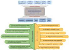
Significance In the past half century, integrated circuits (ICs) supported by complementary metal-oxide semiconductor (CMOS) technology have developed rapidly, which promotes the continuous progress of modern information technology. As the feature size of transistors continues to decrease, the semiconductor-manufacturing process is gradually approaching its limit, resulting in slow or even stagnant improvement of integration. Meanwhile, the system performance is seriously restricted, mainly due to the electronic bottleneck. In addition, with the increase in the number of microprocessors and computing speed, power consumption and heat dissipation due to parasitic effects are becoming the main limiting factors. To break through the bottleneck of conventional IC technology in the post-Moore era, optical interconnects are considered to gradually replace conventional electrical interconnects. Compared with electrical signals, using light as the carrier for signal transmission has its unique advantages, such as large bandwidth, low loss, strong anti-electromagnetic interference capability, and high-speed parallel transmission without crosstalk. Therefore, optical interconnects will undoubtedly become the enabling technology for high-speed data transfer. Concurrently, at the network nodes, conventional optical-electrical-optical signal processing is still limited by the electronic bottleneck. Processing signals in the optical domain offer an effective strategy to increase speed. Consequently, on-chip optical interconnects and processing are paramount to the development of modern high-speed and large-capacity communication networks.The photonic integrated circuit (PIC) is paramount to realize on-chip optical interconnects and processing, which achieves rapid development in recent years. Silicon and III-V are both promising materials for the PIC platform. The main advantage of InP and other III-V materials is that they are direct bandgap materials, which can be used to fabricate semiconductor lasers, amplifiers, modulators, detectors, and other active devices. However, the cost is relatively high and size is relatively large, which limit their large-scale commercialization. By contrast, silicon materials have distinct advantages of large reserves in nature, low cost, almost transparent in the near-infrared and even mid-infrared bands, low loss, and large refractive index contrast of silicon on insulator (SOI), making them suitable for large-scale and high-density integration. Importantly, silicon materials are fully compatible with the existing mature CMOS process, which is essential for developing silicon-based PICs. Since silicon material is an indirect bandgap material, it is impossible to produce high-efficiency light sources. Monolithic integration of all active and passive devices on a single material platform is still challenging. The hybrid integration technology provides a possible solution, which enables the integration of discrete active devices, such as lasers and amplifiers, onto silicon-based passive devices through co-packaging, epitaxial bonding, and monolithic growth to realize low-cost and high-performance hybrid PICs.Although on-chip optical interconnects and processing are the development trends of high-speed communication networks, the sustainable increase of communication capacity is still crucial in the big data era with increasing capacity demand. Notably, photons have multiple physical dimensions, such as frequency/wavelength, polarization, time, complex amplitude, and spatial structure, which can be developed into multiple multiplexing and advanced modulation technologies, making it possible to realize ultra-high-capacity optical communications and interconnects. Wavelength-division multiplexing (WDM), time-division multiplexing (OTDM), polarization-division multiplexing (PDM), space-division multiplexing, and advanced modulation formats have rapidly developed in the past few decades, significantly increasing the transmission capacity of optical communication systems. Therefore, on-chip optical interconnects and processing should also exploit multiple physical dimensions of photons. Particularly, multiple multiplexing technologies and advanced modulation formats can be combined to effectively increase the number of signal channels and aggregate capacity of on-chip optical interconnects and processing systems.Progress Here, we give a comprehensive review of on-chip integrated multidimensional optical interconnects and processing (Fig. 1). The main characteristics of on-chip integrated multidimensional optical interconnects and processing are high integration, small footprint, high reliability, high speed, and low loss. The main contents of optical interconnects include on-chip data transmission of multidimensional optical signals (Fig. 2), on-chip multidimensional multiplexing interconnects of optical signals (Fig. 3), key integrated devices for optical interconnects (Fig. 4), heterogeneous waveguide coupling for optical interconnects (Figs. 5--7), and PICs/optical modules for optical interconnects (Fig. 8). The main contents of optical processing include on-chip wavelength conversion (Fig. 9), on-chip optical frequency comb (Fig. 10), on-chip mode processing (Fig. 11), on-chip polarization processing (Fig. 12), on-chip optical logic and computing (Figs. 13--16), on-chip reconfigurable optical processing (Fig. 17), and on-chip intelligent optical processing (Fig. 18).Conclusions and Prospects With the rapid development of cloud computing and data centers, on-chip integrated optical interconnects and processing have become the key technologies to break through the conventional electronic bottleneck with their unique advantages in integration, speed, bandwidth, power consumption, and multiple physical dimensions. In this article, we review the key technologies and recent progress of on-chip integrated multidimensional optical interconnects and processing. Looking to the future, one would expect the development trend toward multiple materials (III-V, silicon, silicon nitride, silica, polymer, lithium niobate, and 2D material), integrations (hybrid integration, monolithic integration, and integration of photonics and electronics), physical dimensions (frequency/wavelength, polarization, time, complex amplitude, and spatial structure), frequency bands (O+E+S+C+L+U, visible, mid-infrared, microwave, and terahertz), mediums (chip, fiber, free space, and underwater), functions (multifunction, reconfigurable, programmable, and intelligent), and applications (communications, sensing, measurement, imaging, computing, and quantum) (Fig. 19). One typical example would be ultrahigh capacity silicon-based on-chip multidimensional multiplexing and processing system, which consists of an integrated transmitter, integrated receiver, silicon-based multidimensional multiplexing and processing chip incorporating hybrid wavelength/polarization/mode (de) multiplexer, optical switch array, reconfigurable optical add-drop multiplexer array, variable optical attenuator array, and optical power monitor array (Fig. 20).
Jun. 07, 2021Vol. 48 Issue 12 1206001 (2021)
Miao Xu, Haodong Shi, Chao Wang, Zhuang Liu, Qiang Fu, Yingchao Li, Keyan Dong, and Huilin Jiang
Significance Humans need to observe various targets, including space, air, ground, and sea targets. Space targets include satellites, space debris, ballistic missiles, and hypersonic vehicles. Air targets include aircraft, airships, and small craft. Ground and sea targets include surface ships and ground vehicles. The past 20 years have seen an average of 12 collisions between space debris and space payloads every year. In addition, foreign ships and aircraft frequently invade our territorial waters and airspace and repeatedly spy on the activities in our important places. Therefore, the detection, identification, early warning, interception, and even striking of these abovementioned targets are an important and urgent research topic presently.Multidimensional detection based on combined polarization detection, spectrum detection, and other optical technologies can provide the shape, material, location, and other information of the target simultaneously, effectively improving the dimensions and accuracy of space target information. At the same time, with the help of space laser communication, massive information can be quickly and safely transmitted to orbiting satellites and management departments, which can provide the decision-making basis for further disposal in time.Progress In terms of space target detection, the United States has the largest and highest level of space target detection systems, followed by Russia. Europe starts late, but their system has rapidly developed in recent years. China is the latest to start and mainly performs ground-based observations. However, in recent years, China has conducted space-based observation tests and devised various detection methods, including photoelectric observation, radar monitoring, radio detection, and other detection methods.In multidimensional detection, polarization detection technology has the advantages of highlighting the target, penetrating smoke, and identifying the truth and falsehood of the target. Spectral detection technology can distinguish the physical characteristics of the target material. Intensity detection technology has high light energy utilization and resolution, but it also has its own weaknesses. The information obtained by intensity detection is less and easily disturbed by the environment. Moreover, loss of the receiving energy and decrease in imaging resolution can be introduced by polarization detection. Table 1 gives a comparison of the advantages and disadvantages of several detection technologies. Therefore, combining the three abovementioned detection methods to give full play to their own characteristics and advantages helps not only in overcoming the difficulties of space target detection but also in greatly improving the overall detection performance. Changchun University of Science and Technology conducted a multidimensional oil species differentiation test; the test results are shown in Figure 3.The X2000 flight terminal was developed in the United States from the aspect of integrating detection, imaging, and communication. It can realize the functions of bidirectional communication, bidirectional laser ranging, and high-resolution imaging. The United States also proposed the ACLAIM scheme, in which the laser communication antenna and space camera sharing a front telescope and a detector array is employed as the acquisition and tracking system and an imaging receiver. In China, satellite payloads were developed toward the direction of multifunctionality and integration to increase the system function and reduce the volume, mass, and power consumption of the load. This study proposes a new scheme for space target detection and information transmission, which integrates the four functions of laser ranging, spectral polarization imaging, super-resolution imaging, and laser communication into one. The system design and development were performed. Figure 17 depicts the system composition.Conclusions and Prospect In summary, we introduce herein the research status of the technology of multidimensional detection and laser communication integration for space objects and summarize the principle, characteristics, and application of the related technologies. The preliminary research results of our team in the related aspects are as follows: 1) for space object multidimensional detection, the detection mechanism is studied, and a large aperture and a wide field-of-view space-based telescope super-resolution imaging optical system is designed; 2) a prototype of simultaneous and time-sharing polarization imaging detection for complex space targets is developed; 3) ground and sea surface tests are conducted. As regards space laser communication, the optical principle of one-point to multipoint simultaneous space laser communication is proposed for the first time by our team at home and abroad. Accordingly, a principal prototype is developed and a demonstration test is performed. For detection and communication integration, the urgent need for this space security technology is expounded, and the system design idea and a specific implementation scheme are given.Our country should further perform an in-depth research on ultra-high-resolution imaging, full-polarization and hyperspectral multidimensional detection, space- and ground-based combined optical detection, multi-to-multi space laser communication, and integrated laser and microwave network communication to solve the problems of the incomplete detection of low-orbit targets, unclear detection of high-orbit targets, slow response of the dynamic target, and difficulties in numbering space objects, which can provide a technical guarantee for the space security in China.
Jun. 10, 2021Vol. 48 Issue 12 1206002 (2021)
Yongkai Yin, Kai Yu, Chunzhan Yu, Xuechun Bai, Zewei Cai, Xiangfeng Meng, and Xiulun Yang
Significance Light field imaging expands classical optical imaging and provides possibilities for advancement in imaging technology. It has continued to become a major research interest in the field of computational imaging. While, objects and scenes in nature are all three-dimensional (3D) entities, and traditional imaging systems only record two-dimensional (2D) images. From geometry, traditional imaging is equivalent to the 2D projection on the image plane of a 3D object in space. Therefore, the depth information is lost during projection. To restore the object, or perform quantitative analysis on the shape, position, and internal structure of the object, we reconstruct the missing depth information and 3D structure from the 2D images. This process and related techniques are referred to as 3D imaging and have become an essential support technique with applications in areas such as biological imaging, industrial inspection, automatic navigation, and virtual reality. Among several methods for 3D imaging, light field imaging is a major approach.Progress This paper introduces the basic theory of light field while reviewing common systems for light field capture. Key techniques and typical works in light field 3D imaging according to the categorization are discussed. For emphasis, this paper limits its discussion to geometric optics, thus only paying attention to the intensity distribution of rays in 3D space, i.e., the geometric light field. A light field refers to the distribution of radiance carried by rays in 3D space. For monochromatic and static cases, a light field is described using a five-dimensional (5D) plenoptic function. Since radiance remains unchanged along a ray unless blocked, the 5D function reduces to four-dimensional (4D) function in free space. The major challenge choosing a representation for the 4D light field is parameterizing the space of oriented rays. The most common model parameterizes rays using their intersections with two parallel planes ( Fig. 1). The advantages of this representation are that planes can be placed at infinity, and then rays are parameterized by a position and a direction, which is called the parameter/state space of rays. A point in the state space corresponds to a ray in the light field; therefore, phase space (also referred to as ray space) is used to represent the light field ( Fig. 3). From the definition of a light field, we need to record different ray directions passing through any point in 3D space. During imaging using an ordinary camera, only the ray of one direction for each point can be recorded. Therefore, an ordinary camera used in the light field capturing should expand in dimensions such as time, space, and aperture to record rays from multiple directions. Three systems emerge from this (Table 1). They include sequential acquisition (Fig. 6), camera array (Fig. 7), and light field camera (Figs. 8--10). For research in light field imaging, different systems are flexibly selected according to a specific application.The light field carries 3D information of the object and scene. Thus, 3D imaging is realized by modeling and processing the light field data. 3D light field imaging techniques are summarized into two categories: the light field depth estimation and the light field 3D reconstruction. The light field depth estimation obtains the depth (near or far) information about the object. A typical process of light field depth estimation starts with estimating the initial depth map with the appropriate algorithm, and then employing a global optimization or local smoothing algorithm to refine the depth map. The initial depth estimation for a light field is divided into two categories according to the different mechanisms: the method using multi-view stereo (MVS) (Figs. 11--12) and the method using the epipolar plane image (EPI) (Fig. 13). Generally, research on light field depth estimation tends to solve some open problems, e.g., modeling, processing of occlusion, depth estimation of discontinuous surfaces, depth estimation of non-Lambert surfaces, selecting algorithms for depth estimation according to the application, and improving the time efficiency of the algorithm.When applied to measurements, such as 3D positioning and 3D point cloud generation, light field 3D reconstruction is used to obtain the true 3D coordinates. Note that light field 3D reconstruction follows the same theoretical basis as classical binocular and multiview 3D reconstruction, which is hinged on the principle of triangulation. The 3D coordinates are calculated from the intersection of rays in different directions in the 3D space. The light field 3D reconstruction can be divided into active (Fig. 14) and passive (Fig. 15) approaches according to whether the structured illumination is exploited.Conclusions and Prospect Benefiting from the development of photonic and micronano techniques, a series of progress in the research of light field imaging systems and mechanisms has emerged recently. Due to the adoption of new techniques and devices, the quality and structure of the light field data obtained by the new systems are inevitably different from those of traditional systems, which bring new challenges to light field information processing. Depth estimation and 3D reconstruction using a novel light field imaging system are problems worthy of attention. The light field 3D imaging is the support technique for light field imaging. With the scope extension and complex increase in applications, the importance of light field 3D imaging has become increasingly prominent.
Jun. 07, 2021Vol. 48 Issue 12 1209001 (2021)
Zehao He, Xiaomeng Sui, Liangcai Cao, and Guofan Jin
Objective Obtaining high-quality reconstruction is desirable in computer-generated holography. Continuous complex-amplitude computer-generated holograms (CGHs) can present the most enhanced reconstruction quality because accurate amplitude and phase values rather than approximate values are obtained. However, in a practical system, CGHs need to be uploaded on the spatial light modulator (SLM). The most commonly used SLMs can only modulate either amplitude or phase. In addition, SLMs generally have pixelated structures with limited value ranges. It is necessary to sample the continuous distribution into a two-dimensional matrix with specific resolution and discrete pixel values in practical applications. This characteristic may harm the holographic reconstruction quality. Therefore, an optimization method based on parameter space traversal is proposed in this study to evaluate the effect of quantization on the holographic reconstruction quality. Various related parameters are considered in the evaluation. Proper quantization in some specific applications is also suggested.Methods The CGH of a target object is calculated using the angular-spectrum model. In this model, when the reconstruction distance is too large, an aliasing error in the transfer function will be introduced. The maximum reconstruction distance, also called the effective distance, is determined by the Shannon-Nyquist sampling theorem. Meanwhile, when the reconstruction distance is too small, different diffraction orders on the reconstruction plane will interfere with each other. The minimum reconstruction distance is determined by the grating function. To quantitatively evaluate the reconstruction quality, the peak signal-to-noise ratio (PSNR) is used as the index to measure the difference between the reconstructed and target objects. Moreover, a traversal method is used to quantitatively evaluate the influence of quantization. Considering the pixelated structure and discrete value ranges of current SLMs, the continuous complex-amplitude distribution is converted into quantized amplitude- or phase-only distribution by rounding down decimals to integers.Results and Discussions PSNRs of reconstructions via continuous complex-amplitude CGHs are infinite (Fig. 3). No matter how many related parameters, such as resolution, zero-padding area, reconstruction distance, reconstruction wavelength, and pixel pitch change, this conclusion remains unchanged. The calculation and reconstruction of continuous complex-amplitude CGHs were inverse processes. The 8-bit quantization of amplitude in complex-amplitude CGHs induced the degradation of reconstruction quality. The calculation and reconstruction of CGHs were not perfect inverse processes in this situation. However, the difference is negligible (Fig. 4). Compared with results by complex-amplitude CGHs with 8-bit quantized amplitude, results by complex-amplitude CGHs with 8-bit quantized phase presented a worse reconstruction quality. In addition, a zero-padding operation could improve the quality of the reconstruction by CGHs with 8-bit quantized phase. When the size of the target objects was doubled via the zero-padding operation, the PSNRs of reconstructions increased by 6.32 dB (Fig. 5). Phase-only CGHs were obtained by neglecting the amplitude of the complex-amplitude. The neglect of the amplitude had an extremely negative impact on reconstruction quality. PSNRs of reconstruction by phase-only CGHs decreased by 34.77 dB compared with those by complex-amplitude CGHs with 8-bit quantized amplitude. In some specific applications, quantization parameters could be selected appropriately. Phase-only CGHs with 5-bit quantization were proved to be suitable for the applications of dynamic holographic displays. Practically, a look-up table (LUT) often deviates from the designed one. However, a small phase modulation deviation had little effect on the reconstruction quality. In the application of anticounterfeiting, rough calibration for LUT could also be effective (Fig. 6). The reconstruction quality was affected by the quantization of both amplitude and phase. A small increase in the quantization of both amplitude and phase induced a better effect than a huge increase in the quantization of only amplitude or phase (Fig. 8). This conclusion was also applicable when the pixel pitch was less than 1 μm, which would provide guidance for designing meta-surface devices.Conclusions Because of the modulation characteristics of available SLMs, complex-amplitude CGHs with continuous values usually need to be converted to amplitude- or phase-only CGHs with discrete values. The quantization process of approximating continuous values to discrete values has a significant influence on the holographic reconstruction quality. In this study, a traversal method is used to quantitatively evaluate the influence of quantization. Various parameters, such as resolution, zero-padding area, reconstruction distance, reconstruction wavelength, random phase, and pixel pitch are considered. For phase-only CGHs, neglecting the amplitude has an extremely negative impact on reconstruction quality. The PSNRs of reconstruction by phase-only CGHs decrease by 34.77 dB compared with those by complex-amplitude CGHs with 8-bit quantized amplitude. In some specific applications, quantization parameters can be selected appropriately. Dynamic holographic display, holographic anticounterfeiting, and the design of meta-surface devices are discussed specifically. We hope this study will provide a guideline for designing CGH-based systems.
Jun. 10, 2021Vol. 48 Issue 12 1209002 (2021)
Zejin Liu, Weiqiang Yang, Kai Han, and Xiaojun Xu
The development of laser weapons needs to consider the technical challenges, battlefield environment, and combat missions. There are many difficulties in promoting the application of laser weapons, such as high energy and high beam quality laser source, long distance fighting, high efficient damage, high compact design, and actual combat. According to the basic physical principles, this paper discusses and put forward five design criteria of the laser weapons, including high brightness criterion, divergence angles matching criterion, maximum of bucket power criterion, high efficient coupling criterion, and platform fit criterion. These design criteria can provide reference for the research and design of laser weapons.
Jun. 10, 2021Vol. 48 Issue 12 1201001 (2021)
Xiaomin Zhang, Dongxia Hu, Dangpeng Xu, Jing Wang, Xinbin Chen, Jun Liu, Wei Han, Min Li, and Mingzhong Li
Significance High-power lasers enable us to peer deeper into the outer frontiers of the physical world. Since the demonstration of the first pulsed laser in 1960, pushing the limits of accessible laser power has been one of the themes in optical engineering. In this article, we reviewed the progress in developing high-power solid-state lasers and discussed the design issues that determine the performance of these systems.Progress The more one works with a given technology, the more one becomes aware of its limitations—in the case of solid-state lasers, these are primarily the simultaneous availability of high peak and average powers, combined with excellent beam quality in space domain and pulse quality in time domain. In general, the output capability and beam quality of high-power solid-state lasers are essentially limited by five physical limitations categories—gain capability, beam transformation, thermal load, power load, and fluence load. Priority orders of these five limitations largely depend on the application scenario, operational mechanisms, and technical routes of specific laser facilities. For example, for high-power continuous lasers, the main challenge arises from the thermal load limit, while for high-power pulsed lasers, the critical challenge lies in the power load limit. Thus, detailed knowledge of the physics underlying these limitations and their interactions is crucial to the generation of high-quality, high-power lasers.We compiled some recent experimental and theoretical works on the understanding, avoidance, and breakthrough of these physical limitations, as well as relevant enabling developments for high-power solid-state lasers, including novel materials, geometries, and techniques. This paper consists of an introduction, five body sections, and a conclusion. Each section discusses the necessary ingredients for fighting against one of the five physical limitations. These are accompanied by numerous ideas and tips on how to improve the ef?ciency to make maximum use of pump energy.Conclusions and Prospects In conclusion, the core of breaking the gain capability limitation is fighting against the diverse “losses.” The chock point in breaking the limitation of beam and pulse quality is fighting against the diverse “noise” in all the domains of space, time, and spectrum. The key to overcome the limitation of thermal load is combating the thermal effects. Pushing the limit of power load prevents diverse nonlinear optical effects that accompany the propagation of high-power lasers. Furthermore, breaking the deadlock of the fluence load limit helps counteract the inevitable defects in optical elements. During the long struggle of physical limitations with these five categories, a series of novel laser materials, methods, optical techniques, techniques for optics processing, and geometries were correspondingly developed. In addition, theories on the dynamic properties of laser pumping and amplification, propagation, damage, and thermal control were deepened and consummated.We are now on the threshold to reach a new realm of high-power lasers—developing triple-high lasers with high-peak-power, high-energy (i.e., high-average-power), and high-repetition simultaneously. This is a new territory for laser engineering, which requires us to balance conflicting performance parameters. For example, the simultaneous availability of high-peak, average power (high-energy), presents a contradiction because increasing the peak power typically necessitates raising the laser bandwidth, causing an increase in the quantum defect and subsequent ef?ciency loss. This paper intends to be the beginning of a discussion, not the final word, to pave the way for “triple-high lasers.”
Jun. 10, 2021Vol. 48 Issue 12 1201002 (2021)
Yizhou Liu, Wenchao Qiao, Kong Gao, Rong Xu, Tianli Feng, Meng Zhang, Xun Li, Yangyang Liang, and Tao Li
Significance In 1960, after the invention of the first ruby laser, fast-developed solid-state, fiber, gas, and semiconductor lasers provided great support for the research and development of multiple applications, such as optical communication, industrial processing and manufacturing, military and national defense, and state-of-the-art scientific research. Fiber lasers with good heat dissipation characteristics, excellent transverse mode, high amplification efficiency, compact laser construction, and less costs have become the first choice in developing next generation high-power ultrafast lasers. Fiber lasers can achieve long-term operation stability with good beam quality under above-average power because of their waveguide characteristics and large specific gain fiber surface area. High-power ultrafast fiber lasers usually contain four modules, ultrafast fiber oscillators, optical parameters management, ultrafast fiber amplifiers, and nonlinear compression. Ultrafast fiber oscillators provide seed lasers to achieve high-power ultrafast fiber lasers. A qualified mode-locked fiber oscillator has long-term stability and a proportional repetition shared rate corresponding to the requirements of high-power fiber amplifications. Optical parameters management plays a key role in inhibiting uncompensated nonlinear effects and enabling high-energy pulse output with good pulse quality after optical pulse stretching, high power fiber amplification, and optical pulse compression. The ultrafast fiber amplifiers are key modules to scale up the average power of the stretched-signal pulses. Unfortunately, the uncompensated nonlinear phase introduced by the high-peak power of the signal pulse distorts the pulse profile during its propagation in the fiber system. Based on the well-managed optical parameters of fiber lasers, the well-known fiber amplification methods, such as chirped-pulse, divided-pulse, and pre-chirp managed amplifications are making a significant breakthrough in achieving high-power ultrafast fiber lasers. The pulse duration after high-power fiber amplification is hundreds of femtoseconds limited by the gain-narrowing effect. Therefore, a further cascaded nonlinear compression stage is needed for shortening the amplified pulses, which can realize single/few optical cycle pulse duration to fulfill the requirements of the state-of-the-art physical experiments. With their excellent optical characteristics, the fast-developing high-power fiber lasers can play an increasingly important role in multiple applications.Progress Progress in developing ultrafast fiber oscillators, optical parameters management, ultrafast fiber amplifiers, and nonlinear compression are summarized in this paper, and latest published results are discussed by illustrating the advantages and disadvantages of different methods. The highest repetition rate of fiber oscillators reported using the method of nonlinear polarization rotation is 1 GHz provided to be useful in astronomical optical frequency comb, pulse stacking, and the cavity-enhanced high harmonic generation. The highest average output power and pulse energies are 1.98 W and 684 nJ, which are achieved with the nonlinear loop mirror mode-locking scheme, respectively. Applying a semiconductor saturable absorber mirror to the mode-locked fiber laser can generate an output mode-locked laser with the repetition rate range of 10 kHz--1 GHz and sub-μJ pulse energy. As a newly invented mode-locked method, Mamyshev mode-locked fiber laser has attracted attention for its broadband optical spectrum, high-pulse energy output, and high-peak power. As the seeder for a high-power ultrafast fiber laser system, further efforts need to be taken in developing a more stable fiber oscillator with better parameters.Relying on optical parameter management, current ultrafast fiber amplifiers are realized with different amplification methods, such as chirped-pulse, divided-pulse, and pre-chirp managed amplifications. The highest average output power of 830 W at 1 μm was reported by applying the chirped-pulse amplification. Limited by the transverse mode instability and thermal damage threshold, there is one research direction for further improvement that can be realized by searching for new gain materials with better optical performances. Combining the chirped-pulse and multi-channel divided-pulse amplifications, the highest average output power of 10.4 kW was obtained in a 12-channel fiber laser amplifier. 36 fs mode-locked pulses with 100 W average power were achieved with the method of pre-chirp managed amplification, avoiding adding a cascaded nonlinear compression stage. Apart from the aforementioned amplification methods, coherent pulse stacking method is also an efficient way in realizing ultrafast fiber laser with high-pulse energy. Pulse energy of 10 mJ was achieved with the coherent pulse stacking based on the high-power ultrafast fiber laser source.It is difficult to realize sub-100 fs or even shorter pulse durations in a high-power fiber chirped pulse amplification system due to the gain-narrowing effect. Therefore, a further nonlinear compression stage is necessary to satisfying the state-of-the-art applications, requiring short pulse duration. Multipass cells with quartz sheet/noble gas and noble-gas-filled hollow-core fibers are two common constructions in building the nonlinear compression stage, which are illustrated in the nonlinear compression section of this paper. The pulse duration can be compressed to 22 fs, and a pulse energy of 15.6 μJ was realized in the multipass cell construction. Using the noble-gas-filled hollow-core fibers, pulse duration was shortened to approximately 4.3 fs corresponding to a 1.6 optical cycle with a pulse energy of 1 mJ.Conclusions and Prospect In this paper, the high-power ultrafast fiber laser systems are introduced. Research and development status of high-power ultrafast fiber lasers are illustrated along with introducing principles and internal relations of four fundamental modules of ultrafast fiber oscillators, optical parameters management, ultrafast fiber amplifiers, and nonlinear compression. Depending on the fast-developing requirements from multiple state-of-the-art applications, more efforts need to be taken. Further research directions in developing high-power ultrafast fiber lasers have prospected. One promising way is investigating new fiber materials with promising better optical parameters compared to fused silica. Further, making contributions in developing the aforementioned fiber amplification methods is also an efficient way in developing fiber lasers with above-average power, higher-pulse energy, and shorter pulse duration. Newly designed optical fiber amplification methods still need to be invented by carefully considering the optical characteristics of fiber gain material and theoretical nonlinear optical conditions. High-power ultrafast fiber lasers can play a key role in multiple state-of-the-art applications relying on the development of searching for more functional fiber gain materials, optimizing aforementioned amplification techniques, and inventing new methods in amplifying high-power ultrafast fiber lasers.
Jun. 10, 2021Vol. 48 Issue 12 1201003 (2021)
Jingcheng Shang, Yizhou Liu, Shengzhi Zhao, Tianli Feng, Kejian Yang, Wenchao Qiao, Yuantao Zhao, and Tao Li
Significance Optical parametric chirped-pulse amplifier (OPCPA), which relies on the optical parametric process existing in nonlinear crystals to realize pulse amplification, can further enhance a yielded peak power by avoiding the gain narrowing and thermal effects that usually exist in a chirped-pulse amplifier. The generated ultrashort pulse with high peak power from OPCPA can considerably extend the ultrafast pulse to X-ray and infrared regimes, thereby bringing a new revolution to ultrafast science. OPCPA system pumped ultrafast X-ray desktop light source has potential applications in medicine, biology, and materials science. In this article, we review the development of OPCPA systems, including its main characteristics and research progresses in different wavelength regimes (~0.8, ~1.5, ~2, ~3, and >4 μm).Progress In ~0.8-μm OPCPA systems, the pumping laser pulse (0.515 μm) is usually generated via the second harmonic generation process from a Yb-doped laser amplifier. The seed pulses can be generated using a mode-locking few-cycle Ti: Sapphire oscillator directly or via the supercontinuum generation process. The energy/power of seed pulses is usually scaled up inside the BBO nonlinear crystals. The dispersion compensation for the amplified seed pulses is realized by the chirped mirror or glass block. Currently, the highest pulse repetition rate of 11.5 MHz, shortest pulse duration of 5 fs, maximum average output power of 112 W, largest pulse energy of 54 mJ, and highest peak power of 5.5 TW have been realized in the ~0.8-μm OPCPA systems ( Fig. 6). In ~1.5-μm OPCPA systems, the pumping source is a Ti: Sapphire laser amplifier or Yb-doped laser amplifier. The seed pulses are generated via the supercontinuum generation process in noble gas or transparent medium, which is stimulated by the Ti: Sapphire laser oscillator and Er- or Yb-doped fiber/solid-state laser oscillators. Different crystals, such as BIBO, DSTMS (organic crystal), KTA, and LBO, have been employed to amplify the seed pulses. The dispersion of the amplified seed pulses is compensated by the fused quartz, Si, or chirped mirrors. A 350-kHz pulse repetition rate, 6-fs pulse duration, 106-W average output power, 3-mJ pulse energy, and 263-GW peak power have been achieved in the ~1.5-μm OPCPA systems (Fig. 7).For ~2-μm OPCPA systems, the Yb-doped disk laser or Ti: Sapphire laser amplifiers are mainly used as the pumping sources. The seed pulses are generated via the difference frequency generation after the supercontinuum generation process. The seed pulse energy/power is enhanced in a crystal, such as PPLN, LiNbO3, BIBO, or YCOB. The amplified seed pulses are compressed by a high-transmittance crystal, such as Si, ZnSe, or quartz. The optimal output parameters achieved from the ~2-μm OPCPA systems are 100-kHz pulse repetition rate, 10.5-fs pulse duration, 33-W average output power, 3.3-mJ pulse energy, and 132-GW peak power (Fig. 8).A ~3-μm OPCPA system is usually pumped with the Ti: Sapphire laser or Yb-doped lasers. A 3-μm ultrafast pulse can be directly amplified using the ~3-μm OPCPA system or can be the idler pulse from a ~1.5-μm OPCPA system. The employed nonlinear crystals for amplification are PPLN, KNbO3, and MgO∶LiNbNO3. The pulse is compressed with grating pairs or solid medium (Si). The highest pulse repetition rate of 160 kHz, shortest pulse duration of 20 fs, highest average output power of 21 W, largest pulse energy of 5.8 mJ, and highest peak power of 290 GW have been reported from ~3-μm OPCPA systems (Fig. 9).In OPCPA systems operating beyond 4-μm wavelength region, the pump lasers are 1-μm Yb-doped or 2-μm Ho-doped laser amplifiers. In particular, the Ho-doped laser amplifiers are beneficial to realize a high-efficient long wavelength from the OPCPA system. The seed pulses realized from the difference frequency process are amplified by the ZGP, KTA, or LGS(@1 μm). The dispersion management is performed by CaF2, Ge, or grating pair. At present, OPCPA systems can deliver a laser pulse with the longest wavelength of up to 9 μm (Table 2).Conclusion and Prospect Although the performances of OPCPA systems in different wavelength regimes have remarkably improved, there is still scope for further improvement. With the progress of high-power pump laser sources and high-quality nonlinear crystals, the OPCPA system is heading toward achieving shorter pulse duration, larger pulse energy, higher peak power, and longer output wavelength than the existing ones.
Jun. 07, 2021Vol. 48 Issue 12 1201004 (2021)
Ting Fu, Yufei Wang, Xueyou Wang, Jingxuan Chen, Xuyan Zhou, and Wanhua Zheng
Significance Conventional semiconductor lasers typically use gratings, such as distributed feedback (DFB), distributed Bragg reflector (DBR), and slotted surface, to select longitudinal modes and microstructures to select lateral modes, such as narrow ridge, chirped waveguide array, and angled cavity. Even though these technologies are mature, their practicality is limited by output power or complex fabrication processes. For example, a narrow ridge can suppress the high-order lateral modes of the edge-emitting semiconductor laser, thereby limiting the laser's output power due to the small area of current injection. Therefore, new physical effects should be explored to offer new insights into the designs of lasers. Recently, because of the similarity between quantum and optical systems, some physical terminologies of the former are introduced to the latter such as parity-time (PT) symmetry and supersymmetry (SUSY).The PT symmetry can be used to control the laser's spectral and spatial characteristics. The optical system obeying PT symmetry requires that its complex refractive index satisfies the relation, n(x)=n*(-x), which means that the distributions of the real and imaginary parts of the complex refractive index are even and odd functions, respectively. One specified pair of modes of the system can evolve from the PT-symmetric phase to the broken PT-symmetric phase by varying the gain/loss contrast of the PT-symmetric system [Figs. 1(b), (c)]. Especially when the modes stay in the broken phase, the mode field distribution of the amplified mode will be in the gain area and the lossy mode will be in the loss area [Fig. 1(d)], allowing the realization of a single-mode laser. SUSY can also control the optical modes of lasers, making it an excellent candidate for single lateral mode laser arrays. For a waveguide array, the superpartner of the array can be constructed by supersymmetric transformation to couple the high-order modes of the original array but do not influence the fundamental mode (Fig. 3), which can increase the lasing threshold difference between high-order and fundamental modes. Then, the SUSY laser array can exclusively achieve fundamental mode lasing, which improves the laser array's lateral beam quality. Therefore, it is critical to review recent works on the two new methods of optical mode control in lasers.Progress PT symmetry can be realized in the lateral direction of the lasers (Figs. 4--6). Here, the lasing of a single lateral mode can be achieved due to the selective PT symmetric breaking of the fundamental mode, which results from the smaller coupling constant of the fundamental mode than that of high-order mode. When the optical system is PT symmetric, the increased gain threshold between the centered longitudinal modes in the gain spectrum and neighboring longitudinal modes aid the realization of a single longitudinal mode lasing. Furthermore, PT symmetry can be applied to the longitudinal direction (direction along the cavity length). The longitudinally PT-symmetric laser can also realize single-mode lasing because of the PT symmetric breaking of the specified modes (Fig. 7). In addition, coherent perfect absorber (CPA)-laser (Fig. 8) and orbital angular momentum (OAM) laser (Fig. 9) are realized on the basis of longitudinally PT-symmetric microstructures. The double mode spacing of the CPA-laser is observed compared with that of the common Fabry-Perot laser, showing that the neighboring lasing modes move in the opposite direction of the complex plane of frequency when the laser stays in the broken PT-symmetric phase [Fig. 2(f)]. The OAM laser can use the orbital angular momentum of light to transfer information, increase the density of data transmission, and pave the way to develop a multidimensional OAM-spin angular momentum (SAM)-wavelength division multiplexing.Similarly, SUSY can control the optical modes of non-Hermitian systems. The SUSY transformation is used to determine the profile of the refractive index distribution of the SUSY laser array so that the modes are selectively confined in the original array. Simultaneously, the chirped energy pumping increases lasing threshold difference between the selectively confined modes and other modes. If the fundamental mode is confined in the original array and other modes extend to the lossy superpartners, single lateral mode lasing can be realized with higher output power than the single-ridge laser under the same energy pumping density [Figs. 10(a)--(h)]. Furthermore, the second-order SUSY micro-ring laser array is also reported [Figs. 10(i)--(k)], which greatly simplifies large-scale laser array engineering because the superpartner and original array possess identical elements. Also, the second-order SUSY micro-ring laser array emits light in a single lateral mode.Conclusions and Prospect In summary, PT-symmetric lasers that can not only be pumped optically and electrically are realized. However, the methods to suppress the influences of nonlinear effects on the stability of PT-symmetric laser operation should be explored eagerly. Compared with the PT-symmetric lasers, SUSY lasers are still pumped optically. Electrically injected SUSY lasers with multiple coupling terminals are promising candidates for high output power single lateral mode lasers.
Jun. 07, 2021Vol. 48 Issue 12 1201005 (2021)
Wenfeng Cai, Ye Li, Zongyuan Tang, Huilin He, Jiawei Wang, Dan Luo, and Yanjun Liu
Significance A random laser necessitates not a physical resonator, but multiple scattering of photons in an active random medium to bring optical feedback to reach the threshold. This unique principle signifies that random lasers have several characteristics to distinguish them from conventional lasers. Firstly, without a resonant feedback, random lasers can be any geometries, which indicates it reduced greatly manufacturing difficulty and cost. Secondly, the emission spectrum has mutiple narrow spikes, which can be tuned by changing the pump conditions or environment. Thirdly, random lasers have low spatial coherence and large emission angle. Endowing with these superior features, random lasers have been widely used in speckle-free imaging, temperature sensing, medical diagnosis and super-resolution spectrum.After decades of development, scientists have explored a variety of materials as scattering media. Among them, liquid crystals are ideal scattering medium with a tunable disordered degree of the system and orientation of dye molecules. As a result, the laser characteristics of liquid crystal random laser, including threshold, intensity, and polarization, can be well controlled, which provides many potential opportunities for various applications of random lasers.Progress In 1968, Letokhov predicted the existence of random laser theoretically. Scattering of particles increases the distance that photons travel through the medium. The energy density of photons will increase exponentially with time as the strength of scattering and pumping energy increases. If the gain depends on wavelength, the light at this wavelength has a competitive advantage and can be further amplified to form a narrow-band spectrum, which is called spontaneous emission amplification. Meanwhile, the threshold of spontaneous emission amplification in random scattering medium is similar to that of traditional laser. Until 1994, Lawandy confirmed Letokhov's prediction by observing narrow-band emission peaks in amplifying random medium. In 1999, the Cao's group observed several discrete radiation peaks with very narrow spectral linewidth. The results proved the existence of coherent feedback in the random laser.Since the interference effect caused by strong scattering is not considered in Letokhov's theory, the mechanism of the random laser cannot be well explained. In 1999, Cao used ring resonator theory to explain the localization of the random laser. She proposed that in the case of strong scattering, the photon may return to the scatterer from which it was scattered before, creating a closed loop, which plays the role of laser resonator. When the gain of the photon in the closed loop becomes larger than the loss, laser oscillation occurs. Due to the complexity of random laser, up to now there is not an accepted and complete theory that can fully explain the various characteristics of random lasers.In 2006, Liu Jinsong's group used FDTD simulation to study the influence of the degree of orientational disorder of uniaxial scattering medium on the random laser mode in one-dimensional and two-dimensional systems. The results showed that with the increase of the orientational disorder of the liquid crystals, the scattering degree of the system increases gradually, leading to the occurrence of a random laser. Since the orientation of liquid crystal molecules can be adjusted in a variety of ways, we can use liquid crystals to regulate the disorder of the system, and thus improve the laser's Q-value.For nematic liquid crystals random lasers, Ye et al. studied the influence of the liquid crystal cell thickness on the random laser action in the dye-doped nematic liquid crystals system (Fig. 1). Subsequently, Lin et al. investigated the polarization properties of dye-doped twisted nematic liquid crystals in a wedge-shaped cell. In 2019, Naruta et al. prepared a dye-doped random laser with ferromagnetic nematic liquid crystal, which could be tuned by the magnetic force. In 2006, Liu et al. studied the characteristics of dye-doped polymer-dispersed liquid crystals (DD-PDLC) random laser (Fig. 6). In 2019, Dai et al. realized the magnetically tunable DD-PDLC random laser by doping magnetic nanoparticle. Lee et al. previously proposed an optically controlled method of DD-PDLC random laser by doping the azo dye.For cholesteric liquid crystal (CLC) random laser, in 2012, Morris et al. realized selective emission of random lasers and band-edge laser by changing the frequency of the applied electric field (Fig. 9). In addition, Huang et al. proposed a CLC finger texture reconstruction method based on electric field induction, resulting in flexible modulation of laser wavelength and multiple modes (Fig. 10). In 2018, Hu et al. utilized liquid crystal multiple scattering and near-infrared controlled photothermally band gap tuning to achieve a random laser. In 2020, the group also constructed polymer-stabilized CLC to achieve random laser emission with low coherence and wide tuning range (100 nm) at the band edge.For blue phase liquid crystal (BPLC) and polymer-stabilized blue phase liquid crystal (PS-BPLC), Lin et al. studied random lasers based on coherent feedback in BPLC and PS-BPLC in 2012 (Fig. 11). In 2020, Luo's group demonstrated a spatially and electrically tunable random lasing based on PS-BPLC-wedged cell (Fig. 12). In 2020, Chauhan et al. proposed a random laser based on spatially-assembled dye-doped BPLC microdroplets (Fig. 14). Wang et al. studied bichromatic coherent random laser from dye-doped PS-BPLC controlled by pump light polarization.When metal nanoparticles are combined with a disordered active medium, the scattering intensity can be significantly increased. In addition, it can increase the laser gain and reduce the random laser threshold through localized surface plasmon resonances (LSPR). Deng's group has done a lot of research on the plasmon-enhanced liquid crystal random laser.Conclusion and Prospect Though there is significant progress on the liquid crystal random lasers, their mechanisms remain to be further explored. Future development can be made in the following aspects including further reduced threshold, directionality and polarizations, electrical pumping, miscibility between liquid crystals and novel gain media, etc. Significant performance improvement of liquid crystal random lasers is of great importance for the practical applications and commercialization.
May. 21, 2021Vol. 48 Issue 12 1201006 (2021)
Zijing Li, Lili Yan, Peng Zuo, Liangyue Xie, Zhiqiang Li, and Bing Jin
Significance Femtosecond laser technology plays an important role in the study of ultrafast dynamics of light-induced reactions. Many ultrafast spectroscopy techniques, such as transient absorption spectroscopy, ultrafast Raman spectroscopy, and ultrafast photoelectron spectroscopy/imaging, are widely used in scientific research in the fields of physics, chemistry, biology, and materials science.At present, the laser wavelength range produced by mature commercial femtosecond lasers is mainly limited to infrared, visible, and ultraviolet (UV) bands. When the absorption spectrum or ionization energy of a sample is in the vacuum ultraviolet (VUV) band below the wavelength of 200 nm (~6 eV), commercial femtosecond laser pulses are insufficient for achieving single-photon excitation/ionization of a sample. The two-photon or multiphoton absorption of long-wavelength lasers leads to low excitation/ionization efficiency compared with the single-photon process.In the past two decades, the technology for developing a miniaturized tabletop femtosecond VUV laser source using commercial femtosecond lasers (such as Ti:sapphire laser) in laboratories has advanced rapidly. This review briefly introduces four-wave mixing (FWM) techniques, which are widely used in a tabletop femtosecond VUV laser source. This work mainly focuses on the development of FWM in gas-filled hollow fibers and filaments.Progress An early femtosecond VUV laser system was capable of producing tunable femtosecond VUV pulses by two-photon near-resonant four-wave difference-frequency mixing in argon (Fig. 3). To generate VUV pulses using the four-wave difference-frequency mixing scheme, high-intensity femtosecond laser pulses are required as a driving source. Moreover, only a part of the incident spectrum can contribute effectively to the frequency-mixing process, thereby leading to spectrally narrowed and temporally lengthened VUV pulses. Therefore, this near-resonant requirement limits the phase-matching bandwidth, tunability, pulse width, and conversion efficiency.FWM is achieved by converting the frequency of ultrashort-pulse Ti:sapphire laser pulses from visible light into deep UV light using a hollow-fiber geometry (Fig. 4). Collinear phase matching using off-resonant χ(3) processes in a hollow fiber to generate VUV light is more efficient and generates broader bandwidths than past schemes. It is confirmed that the conversion efficiency can be significantly improved by exciting higher-order transverse modes and coating the inner surface of the hollow fiber with aluminum.Another method for producing ultrafast VUV pulses is developing FWM in a filament (Fig. 6, Fig. 7, and Fig. 9). Typically, considerably more energy-driving pulses can be used in a filament than in a hollow fiber. Furthermore, the alignment of two laser beams, e.g., the third harmonic and fundamental of a Ti:sapphire laser, in a gas cell is considerably easier than in a narrow hollow fiber. Intensity clamping and mode-cleaning effects of filamentation provide stable and spatially clean output pulses.In contrast to the above-mentioned FWM schemes, VUV pulses with remarkable high pulse energies can be generated via a third-harmonic generation process (Fig. 10). However, the conversion efficiency of the high-harmonic generation process from fundamental radiation is low, and it is desirable to avoid such a significant loss of VUV pulse energy. A short-wavelength driving laser eases this difficulty.To acquire tunable femtosecond VUV pulses, the use of optical parametric amplifier (OPA) or noncollinear optical parametric amplifier (NOPA) systems is considered (Fig. 11). Although it is convenient to produce continuously tunable femtosecond pulses using OPA or NOPA systems, the wavelength range covered by continuously tunable tabletop VUV lasers is limited.Conclusions and Prospects In the past two decades, the development of tabletop femtosecond VUV laser sources has made great progress. The demand for developing femtosecond VUV laser sources is increasing in tandem with the advancement of scientific research and application. In the future, it is critical to improve the frequency up-conversion efficiency of the high-harmonic generation/FWM process and continuously investigate the development and application of new nonlinear media.
Jun. 10, 2021Vol. 48 Issue 12 1201007 (2021)
Jiaqi Zheng, Zhenhua Cong, Zhaojun Liu, Shang Wang, and Zhigang Zhao
Significance Ultrafast lasers with pulse durations on the orders of picosecond and femtosecond are widely used in various fields, such as supercontinuum generation, photoelectron microscopy, and material micromachining. The traditional high-power ultrafast lasers with repetition rates of kHz-MHz exhibit a large heat-affected zone during material micromachining, leading to unpleasant damage to the materials. The emergence of pulse lasers with ~GHz repetition rate can effectively solve this problem. Combining the very high repetition rate of ~GHz and novel burst mode processing technique, the GHz “burst-mode” femtosecond lasers have been used to ablate the target materials before the residual heat deposited by previous pulses diffuses away from the processing region, which can not only improve the ablation efficiency, but also ensure excellent processing quality.Due to its short wavelength, high resolution, and high photon energy, deep ultraviolet (DUV) lasers are widely used in chip defect detection and photoelectron spectroscopy experiments. In order to obtain DUV lasers with high beam quality, high coherence and high repetition rate, near-infrared all-solid-state lasers are usually used as the fundamental drivers to DUV lasers through the nonlinear optical crystals-based multi-stage frequency conversion technique. Due to the high peak powers and high wavelength conversion efficiencies of the near-infrared pulsed lasers with repetition rates of kHz and MHz, it is easy to obtain high-power DUV lasers for lasers with those repetition rates. At present, the repetition rates of industrial high-power ultraviolet lasers are usually in kHz and MHz range. There are very few research results on DUV lasers with ~GHz repetition rate, which greatly limits the application potential of DUV lasers in the above aspects.In recent years, various methods have been proposed to achieve DUV laser pulses with repetition rates of ~GHz. However, these methods still face a series of challenges. Therefore, it is necessary to summarize recent development tendency of technology of high repetition rate ultrashort laser pulse generation and frequency conversion.Progress There are many methods for producing GHz bursts of laser pulses. Femtosecond pulses at multi-GHz repetition rates can be obtained directly from the oscillators with harmonic mode-locking technique, semiconductor saturable absorber mirror and Kerr lens based passive mode-locking techniques. Typical pulse repetition rates of pulse trains generated by mode-locked fiber oscillators are in the range from tens up to hundreds of MHz. The GHz pulses can be obtained through repetition rate multiplication techniques. In this study, we briefly illustrate their pros and cons and review their recent developments. The emergence of multi-stage amplification systems has increased the average power of ~GHz femtosecond pulses in the near-infrared band to the order of hundreds of watts (Table 1).There are many methods for producing DUV lasers. For the method of nonlinear crystal frequency conversion, the research of 266/258 nm DUV nanosecond lasers (Table 3), picosecond lasers (Table 4) and femtosecond lasers (Table 5), as well as 213/206 nm (Table 6) and 193 nm DUV lasers (Table 7) in the past two decades are summarized. Nowadays, the average powers of high power 355 nm ultraviolet lasers have reached hundreds of watts, and the market is relatively mature. Although commercialization of DUV lasers with wavelength below 300 nm is still not mature, the current 266 nm laser developed in the laboratory can achieve an output average power of 50.1 W, which is about to enter the order of 100 W, and has passed the stability test for more than 5000 hours of continuous operation.For high power GHz repetition rate near-infrared femtosecond pulse lasers, the difficulty lies in the generation of GHz seed. For GHz repetition rate amplifier, it is relatively easy to obtain higher average powers due to low single pulse energy and low peak power. For GHz repetition rate DUV femtosecond pulse laser source, the difficulty is not in the generation of the fundamental frequency laser, but in the low peak power of the fundamental frequency laser and the thin nonlinear medium used, which leads to low nonlinear frequency conversion efficiency, and it is difficult to obtain GHz femtosecond pulse laser in the DUV band (Fig. 6).Conclusion and Prospect In recent years, the French company Amplitude has put forward the idea of “GHz Revolution”, which mainly refers to the development of ultra-short pulse laser sources with pulse repetition rate in GHz. The emergence of multi-stage amplification systems has increased the average power of GHz femtosecond pulses in the near-infrared band to the order of hundreds of watts, which successfully solves the problem of the GHz pulse in industrial processing. Therefore, the development of high-power near-infrared band GHz repetition rate pulse lasers is relatively mature at present. Coupled with the continuous improvement of nonlinear frequency conversion technology, DUV laser repetition rate has entered the GHz. Although the industrialization and commercialization of DUV laser techniques still face some problems, such as easily damaged crystal coating, low wavelength conversion efficiency of DUV lasers, and long-term unstable operation of high-power DUV lasers, these problems have been gradually solved in practice. With the further maturity of frequency conversion and power amplification techniques, perhaps kilowatt-level DUV lasers will appear in the next 5-10 years, all of which will certainly make a breakthrough in the secondary laser source based on ultraviolet laser and DUV laser.
Jun. 07, 2021Vol. 48 Issue 12 1201008 (2021)
Jun Meng, Zhenhua Cong, Zhigang Zhao, Shang Wang, Yunxuan Qi, Xingyu Zhang, and Zhaojun Liu
Objective Laser sources at 1.5 μm, providing high pulse energies and short pulse durations are used in various applications, such as electro-optical countermeasures and high precision ranging. Lasers at 3--5 μm are used as lighting sources for active remote sensing and gas detection, which show important potential applications. Therefore, lasers with high energy at both wavelength bands have become research hotspots. The optical parametrical oscillators (OPO) are effective ways to generate lasers with wavelengths at 1.5 μm and interval 3--5 μm due to their compactness, wavelength-tunable property, and potential for generating high energy and short pulse width. Presently, the major nonlinear crystals with high-quality include biaxial crystals such as KTiOAsO4 (KTA), KTiOPO4 (KTP), ZnGeP2 (ZGP), and periodically poled crystals such as PPKTP, PPLN, PPLT, etc. KTP crystals are used to obtain lasers at 1.5 μm, which is affected by severe absorption in the mid-infrared region. To obtain lasers at 3--5 μm, ZGP crystals have been under investigation for a long time. However, 2 μm pump sources are more in need, which is technically more difficult than their 1-μm counterpart. PPLN crystals are used to obtain mid-infrared lasers. Compared with crystals such as KTP, the damage threshold of PPLN crystals is lower. KTA and KTP crystals belong to the same crystal group and have a high damage threshold (>600 MW/cm 2), large nonlinear coefficient (d24=3.2 pm/V), large acceptance angle, a wide temperature range, and stable physical and chemical properties. The transmission performance of KTA crystals in the mid-infrared band (3--5 μm) must be better than that of KTP crystals. These characteristics make KTA crystals suitable for high energy mid-infrared laser applications. In this study, we report a 100 Hz high energy KTA crystal-based OPO system. Methods The 100 Hz high energy KTA-OPO system is composed of 1064 nm Nd: YAG main oscillator power amplifier (MOPA) and KTA crystal-based OPO. The Nd∶YAG MOPA laser at 1064 nm served as the pump source. To obtain high beam quality, the Nd∶YAG MOPA system adopted the “unstable cavity oscillator + two-stage amplifiers” scheme. Both the oscillator and the two-stage amplifier used a double rod structure connected in series, and a 90° quartz rotator between the two Nd∶YAG crystal rods to compensate for the thermal depolarization effect. To prevent self-excited oscillation and spontaneous radiation between the stages while protecting the optical components of each stage, isolators are placed between each stage. The X-cut KTA crystal is used in the experiment, and the dimension of the KTA crystal is 10 mm×10 mm×33 mm. The cavity is designed as a signal resonant oscillator with a cavity length of 65 mm. The input mirror is coated to be highly reflective for the signal and high transmittance for the pump light. The output mirror is coated with a partial reflectivity of 50% for the signal and high transmittance for the idler. The pump light passed the OPO twice. An isolator protects the pump laser from the remaining pump light that comes back from the OPO cavity.Results and Discussions A homemade 1064 nm Nd∶YAG MOPA with a pulse energy of 580 mJ at 100 Hz repetition rate is employed as the pumping source. After two-stage amplification, 580 mJ of 1064 nm laser is obtained with the extraction efficiency of the primary amplifier and secondary amplifier at 6.7% and 10.8%, respectively (Fig. 3). The beam quality factor of the 1064 nm laser is Mx2=4.6 and My2=3.7 (Fig.4). The pulse width of the laser from the oscillator and primary amplifier and secondary amplifier are 15.3, 16.9, and 18.0 ns, respectively (Fig.5). In the OPO experiment, the optical-to-optical conversion efficiency is optimized by increasing the cavity length and KTA crystals length. The output energy and conversion efficiency of the KTA crystal with a length of 33 mm are higher than that of the KTA crystal with a length of 38 mm (Fig.6). Then, experiments with different OPO cavity lengths are performed on the 33-mm KTA crystal. The results indicated that the output energy and conversion efficiency are higher for short cavity length (Fig.6). The threshold of the OPO is about 20 mJ. When the pump energy is 580 mJ, 64 mJ idler is obtained at 3.47 μm and associated signal at 1.54 μm is 178 mJ (Fig.7). The OPO efficiency is 46.3% high, and OPO output stability is 1.2% rms (Fig.7). The pulse width of the output laser at 1.54 and 3.47 μm is 13.7 and 11.8 ns, respectively (Fig.8). The beam quality factor of the 1.54 μm laser is Mx2=30.5 and My2=28.2 (Fig.9). In addition, the center wavelength of the signal laser is 1.535 μm (Fig.10).Conclusions A 100-Hz, high-energy KTA crystal-based OPO system is reported. A homemade 1064 nm Nd∶YAG MOPA with a pulse energy of 580 mJ at a 100 Hz repetition rate is used as the pumping source. We adopted plane-plane cavity configuration for the OPO, and an X-cut KTA crystal as the nonlinear crystal. The obtained pulse energies at a signal wavelength of 1.53 μm and idler wavelength of 3.47 μm are 178 and 64 mJ at a pulse repetition rate of 100 Hz, respectively. Furthermore, the pulse durations are 13.7 and 11.8 ns, respectively, and the optical-to-optical conversion efficiency is 43.6%.
Jun. 07, 2021Vol. 48 Issue 12 1201009 (2021)
Yongyao Xie, Zhenhua Cong, Zhigang Zhao, Xingyu Zhang, Xian Zhao, Xianbin Shao, Wei Zhao, and Zhaojun Liu
Objective Single-frequency fiber lasers (SFFLs) are widely used in areas of coherent beam combination, gravitational wave detection, lidar, and nonlinear frequency conversion because of their excellent performance. In particular, SFFLs operating at 976 nm are highly demanded for nonlinear wavelength conversion to generate coherent blue light. SFFLs use either a ring- or linear-cavity configuration. The ring-cavity setup is complicated because many additional components must be inserted to enable a single-frequency output, which unavoidably introduces insertion loss. In addition, the stable single-frequency operation of a ring-cavity fiber laser is susceptible to environmental changes and vibrations, thereby resulting in mode hopping. In comparison, linear-cavity construction, such as the distributed Bragg reflector (DBR) scheme, is more compact, which creates a large longitudinal mode spacing, helping to maintain lasing on a stable single longitudinal and hop-free mode. The cavity length of DBR SFFL is limited to only a few centimeters. Therefore, high-gain fibers are demanded to enable sufficiently high gain. A novel Yb∶YAG crystal-derived fiber (YDSF) that exhibits some unique properties in fiber lasers has been developed. The YDSF was fabricated based on a molten core method (MCM) and shows advantages such as high doping levels and high stimulated Brillouin scattering threshold. In addition, the pure silica cladding of the YDSF makes it highly compatible with commercially available silica fiber devices. All the above mentioned characteristics make the YDSF suitable for high-power single-frequency lasers. Based on these fibers, single-frequency lasers emitting at 1 μm have been demonstrated recently. In 2019, we demonstrated a 110-mW single-frequency YDSF laser at 1064 nm. However, to the best of our knowledge, single-frequency YDSF lasers below 1 μm have never been reported.Methods A commercially available 10% (atomic number fraction)Yb∶YAG crystal was used to prepare a YDSF. In the experiment, the entire preparation process was divided into two steps to maintain the uniformity of the optical fiber. First, a rod fiber having a diameter of ~1.7 mm was fabricated using a 1.6-mm YAG crystal and pure silica tube (Dinner=2 mm, Dexternal=10 mm). The drawing temperature was controlled at ~2000 ℃. Second, the YDSF was fabricated based on the rod fiber. A short piece of rod fiber was inserted into a different silica tube with the same specification to constitute a new preform, which was drawn into the fiber at 1940 ℃. Next, the physical and optical properties of the YDSF were measured using some devices and methods, such as an optical microscope, energy dispersive spectrometer, fiber refractometer, and cut-back method. Afterward, a homemade all-fiber amplifier was used to measure the gain coefficient of the YDSF at 976 nm. Then, the laser performance of the YDSF was investigated by optimizing the gain-fiber length and reflectivity of fiber Bragg grating (FBG). In addition, a DBR SFFL based on an 8-mm-long YDSF was built to further verify the performance of the YDSF.Results and Discussions The mass fraction of SiO2 and Yb2O3 in the core region of the YDSF were measured to be 58.83% and 5.25%, respectively (Fig. 1). As expected, interdiffusion occurred between the Yb∶YAG core and silica cladding during the drawing process. The refractive index profile of the fiber cross section was measured; the numerical aperture (NA) of the core with a diameter of 8.7 μm was 0.5 (Fig. 1), indicating that the YDSF was a multimode fiber. The absorption peaks of the YDSF were located at 915 nm and 976 nm, corresponding to the transitions from the ground state 2F7/2 to higher states of 2F5/2 of Yb 3+. The peak absorption coefficients were 6 dB/cm and 30 dB/cm for 915 nm and 976 nm, respectively (Fig. 1). For a signal power of 0 dBm and pump power of 181 mW, the net gain coefficient of the YDSF reached 12.6 dB/cm (Fig. 2), which indicated that the YDSF could be used as a gain medium for a 976-nm laser. By optimizing the gain-fiber length and reflectivity of FBG, a maximum output power of 37.2 mW was obtained with a slope efficiency of 24.3% (Fig. 3). In addition, using the 8-mm-long YDSF as the gain medium, a 976-nm DBR SFFL was demonstrated. A maximum output power of 17.8 mW with a signal-to-noise ratio (SNR) of >45 dB was obtained at a launched pump power of 203 mW, and no output power saturation was observed. The corresponding slope efficiency was 15.1% (Fig. 5), which was low because of the mode mismatch. More efforts should be made for reducing the NA and improving Yb 3+ doping concentration. The linewidth of the laser was measured to be less than 41 kHz, which was limited by the measurement setup (Fig. 6). The beam quality of the laser output was also measured using a charge-coupled device (Thorlabs, BC106N-VIS); the beam quality factor was measured to be 1.01 and 1.02 in the horizontal and vertical directions, respectively (Fig. 5). Conclusions A YDSF with 5.25% Yb2O3 doping concentration(mass fraction) was fabricated using MCM. The transmission loss of the YDSF with a core diameter of 8.7 μm was measured to be 1.29 dB/m at 1550 nm. The gain coefficient of the YDSF was 12.6 dB/cm at 976 nm with a pump absorption coefficient of 6 dB/m at 915 nm. Using the DBR linear cavity, a 17.8-mW single-frequency laser at 976 nm was achieved with an 8-mm-long YDSF, exhibiting a slope efficiency of 18.5%. To the best of our knowledge, this is the first demonstration of a single-frequency YDSF laser below 1 μm. The SNR was measured to be >45 dB with a linewidth of less than 41 kHz. Results indicate that the YDSF is a promising candidate material for the SFFL operating in the 976-nm wavelength region.
Jun. 07, 2021Vol. 48 Issue 12 1201010 (2021)
Hongwei Chu, Shengzhi Zhao, Kejian Yang, and Dechun Li
Significance Nonlinear optical materials have become increasingly essential to various fields, such as optoelectronics, communication, and information processing. Therefore, there is an urgent need to develop new and excellent nonlinear optical materials. Compared with traditional inorganic nonlinear optical materials, organic nonlinear optical materials have decisive advantages in damage threshold, response time, and nonlinear optical coefficient. Zeolitic imidazolate frameworks (ZIFs) are of special metal-organic frameworks with imidazole or its derivatives as ligands. Due to their structural diversity, high thermal and chemical stabilities, they have been repeatedly researched worldwide in recent years.Progress Metal-organic materials having large π-electron conjugation systems or low charge-transfer excited states are used as nonlinear optical materials. Although organometallic materials exhibit considerable nonlinear optical properties over a wide wavelength range, their photostability and thermal stability properties limit their applications. Research has confirmed that metal-organic coordination polymers and frameworks effectively improved stability while maintaining several nonlinear optical properties. This review selected two ZIFs, ZIF-8 and ZIF-67, and discussed the recent progress in their synthesis, preparation, and nonlinear optical properties. ZIF-8 and ZIF-67 are commonly synthesized using the solvothermal method, room-temperature magnetic stirring method, and other ultrasound or microwave assistant methods. Recently, most micro-nano crystals with excellent physiochemical properties and stable structures are prepared in terms of ZIF-8 and ZIF-67. Alternatively, in the nanosecond framework structure of metals, the nonlinear optical properties are enhanced by careful design of molecular symmetry, π-electron conjugation length, intramolecular charge-transfer mechanism, and interaction among molecules. Phenomena such as multiphoton absorption, upconversion, and excited light are realized. Both ZIF-8 and ZIF-67 exhibited interesting nonlinear optical properties due to advanced structural designs on ZIFs. In 2016, it was proven that ZIF-8 possessed a large effective nonlinear coefficient of -0.25 pm/V, with link reorientation, the nanocrystal defects reduced the nonlinear second harmonic generation due to the induced inversion center, as in Fig. 3. With the cobalt (Co) ions induced in ZIF-8, the size of the synthesized ZIFs increased. Researchers have found that the absorption at 1125 nm was enhanced because of the transition between 4A2→ 4T1(F) in Co ions. Following these consequences, we investigated the nonlinear absorption coefficient, two-photon absorption cross-section, nonlinear refractive index, and third-order optical susceptibility of the ZIF-67 sample prepared using the solvothermal method. Results showed that the two-photon absorption cross-section was approximately 85×10 5 GM, the nonlinear refractive index was ~ -9.3×10 -4 cm 2/GW, and the third-order optical susceptibility was -8.2×10 -11 esu at 1 μm. Our results confirmed that ZIF-67 possessed excellent nonlinear optical properties, suitable for optical modulators, limiters, and detectors. Conclusions and Prospects This review summarizes advances on the preparation and nonlinear optical properties of ZIF materials worldwide. ZIF-8 and ZIF-67 are examples of such organometallic nano framework material. ZIFs show good nonlinear optical properties, such as high modulation depth, large third-order nonlinear polarizability, nonlinear refractive index, low extinction coefficient, etc. It has important application value in electronics and optoelectronics.However, the research of ZIF nanomaterials is concerned, there are still a series of problems to be solved.1) The microscopic mechanism of photogenerated carriers is yet to be sufficiently explored. A large blank on how to generate, separate, combine, and manipulate the electron-hole pairs remains unresolved.2) How the interaction between the metal ions and organic linkers affects the nonlinear optical properties? How to optimize the ratio and synthesis of metal ions and organic linkers? How to control and manipulate the synthesis conditions and solutions? The answers to these questions are key advancements in the preparation and investigation of ZIFs and its nonlinear optical properties, respectively.3) The application of ultrafast photonics of ZIFs based on nanomaterials, especially the realization of ultrafast laser, is another work of urgent consideration.
Jun. 07, 2021Vol. 48 Issue 12 1203001 (2021)
Mingyang Wei, Jie Lian, Qingfen Jiang, Yu Zhang, Chenlin Wang, Yueming Wang, and Zhen Xu
Objective Recently, two-dimensional materials, particularly transition metal sulfides, have attracted broad attention in the field of optoelectronics because of their unique properties. Platinum diselenide (PtSe2) is a new type of transition metal sulfide material with unique features, such as adjustable bandgap and high carrier mobility, that has excellent potential for saturable absorbers, photodetectors, and photovoltaic cells. It is necessary to study the variation of PtSe2 optical properties with the number of layers, which is essential for designing and optimizing related devices. Moreover, it is also valuable to study the change in the refractive index of PtSe2 films with temperature in practical applications. In this work, PtSe2 films with two, four, and six layers were grown on sapphire substrates using the chemical vapor deposition method. The optical properties of PtSe2 with different thicknesses, including optical bandgap, refractive index, extinction coefficient, dielectric function, and thermo-optical coefficient, were investigated using the spectrophotometer and spectroscopic ellipsometry. This work can guide the design and optimization of PtSe2-based optical modulation devices.Methods The synthesis method of PtSe2 films used in this work is the three-zone temperature-controlled chemical vapor deposition method (Fig.1). PtSe2 films with two, four, and six layers were grown on sapphire substrates by controlling the growth time. The thickness and surface morphology of the samples were confirmed using atomic force microscopy. The Raman vibration patterns of samples with different layer numbers were investigated using Raman spectroscopy. The samples' absorption spectrum was obtained using the spectrophotometer, and the optical bandgap of the samples was obtained using the Tauc formula. The optical constants and dielectric functions of PtSe2 with different layer numbers were obtained using spectroscopic ellipsometry. Three Tauc-Lorentz oscillators were used to describe the dielectric function of the PtSe2 films during the analysis of elliptical polarization spectra. In addition, we studied the refractive index and extinction coefficient of PtSe2 with increasing temperature using spectroscopic ellipsometry and a high-temperature thermal bench. The thermo-optical coefficients of four-layer and six-layer PtSe2 films were calculated.Results and Discussions The prepared PtSe2 films have good homogeneity and the transmittance decreases as the number of layers increases (Fig.2). Raman spectra show that PtSe2 has three main Raman vibrational modes, and the Eg and A1g modes are red-shifted as the number of layers increases (Fig.3). This phenomenon can be attributed to the increase in interlayer coupling. The absorption spectra and Tauc formula calculations show that the optical absorption increases and the bandgap decrease as the number of sample layers increases (Fig.4). The bandgaps of the two-layer, four-layer, and six-layer PtSe2 films are 1, 0.85, and 0.73 eV, respectively. The spectroscopic ellipsometry spectrum of PtSe2 was modeled using three Tauc-Lorentz oscillators, and the optimum fitting parameters were obtained (Table 1). By fitting the ellipsometric parameters of the PtSe2 films, the optical constants of the samples with different layers, including the refractive index, extinction coefficient, and the real and imaginary parts of the dielectric function, were obtained (Fig.6). The results show that the optical constants of PtSe2 films are significantly correlated with both wavelength and thickness. In the wavelength range of 300-700 nm, the refractive index of PtSe2 films increases with wavelength until it reaches a certain wavelength and then starts to decrease slowly. This transition wavelength is also red-shifted with the increase in the number of layers. This may be related to the increase in the interlayer coupling as the number of layers increases. Alternatively, as the number of layers increases, the peak position of the imaginary part of the dielectric function is also red-shifted, indicating that the electron leap energy between the conduction and valence bands is decreasing. In addition, the variation of the refractive index and extinction coefficient of PtSe2 with temperature was obtained from variable-temperature spectroscopic ellipsometry measurements (Fig.7). The thermo-optical coefficient of PtSe2 as a function of wavelength was obtained (Fig.8). As shown in Fig.8, the thermo-optical coefficient is around the zero-axis between the wavelength of 400-500 nm, indicating that the refractive index of PtSe2 hardly changes with temperature in this band and has good thermo-optical stability.In contrast, the thermo-optical coefficient is negative within the wavelength of 500-800nm, indicating that the refractive index decreases with an increase in temperature. It may be related to the semi-metallic properties exhibited in multilayer PtSe2 films. Therefore, PtSe2 films are more suitable for application within optoelectronic devices operating in the wavelength range of 400-500 nm.Conclusions Continuous PtSe2 films with two, four, and six layers were grown using chemical vapor deposition. Raman spectra indicated the existence of interlayer coupling in the samples. The bandgap, refractive index, extinction coefficient, and the dielectric function of the samples were characterized using the spectrophotometer and spectroscopic ellipsometry, and the results showed that the bandgap and optical constants of PtSe2 were significantly correlated with the thickness. The effect of temperature on the optical constants of PtSe2 was analyzed using variable temperature ellipsometric spectroscopy, and the thermo-optical coefficients at different wavelengths were obtained. The result shows that the thermo-optical coefficient is near the zero-axis between the wavelength of 400-500 nm. In contrast, the thermal-optical coefficient is negative in the wavelength range of 500-800 nm, which may be related to the semi-metallic nature of PtSe2 multilayer films. This research can guide the design and optimization of PtSe2-based light modulation devices.
Jun. 10, 2021Vol. 48 Issue 12 1203002 (2021)
Shaorong Xiao, Bohan Liu, Liufeng Shi, and Biao Huang
Objective Visibility measurement is not only used for weather forecasting but also widely used in aviation, voyage, highway, military, and environmental monitoring. In the visibility observation, the instrument measurement replaces manual observation. Currently, the mature visibility measuring instruments have transmission-and scattering-types. Advantage of the transmission type is that it can detect atmospheric transmittance without any assumptions about the atmospheric conditions. Owing to the large sampling volume and high accuracy, the transmission visibility meter is widely used in airports. Since several years, the World Meteorological Organization has been conducting a tracking study on measurement errors of visibility meters distributed globally. The results showed that the main reason for measurement uncertainties is the incorrect alignment of the transmitter and receiver. Errors caused by this incorrect alignment can be attributed to spot drift, which is projected by the detection beam on the sensitive area of the detector. In this paper, the influences of photodiode on the uncertainty of the visibility measurement were reported, law of the influence of spot drift on transmission visibility measurement uncertainty was found, and strategies to suppress the effects of beam drift were presented.Methods The photodiode spectral response distribution equation was derived based on the quantum conversion efficiency. In transmission visibility meters, photodiodes with large sensitive areas are the most general choice because of their full energy utilization. However, the size of a sensitive area has its limitations; the spectral response on the sensitive area is not distributed uniformly because the edge of the sensitive area is the recombination center of photogenerated carriers, which implies that the output current of the photodiode is different when light spot with the same power beam drifts at different positions. An experimental visibility receiver setup for verification was constructed, and two photodiodes made by different manufacturers were selected. Their nominal sensitive surface area was 6.0 mm×6.0 mm, and diameter of the light spot projected on the sensitive surface was approximately 0.3 mm. A micrometer was used to determine the position of the light spot on the sensitive area, and a low-noise I/V circuit was proposed to detect the output current of the photodiodes. The I/V circuit output voltage could be acquired by a high-precision digital voltmeter. To reduce the influence of the laser output changes, a standard laser power meter was used to monitor the laser output power during the experiment. In the experiment, the light spot was always located in a sensitive area. The spectral response distributions of the two photodiodes were measured separately, and the contribution of voltage offset error to the uncertainty of visibility measurement was derived according to Koschmieder's law.Results and Discussions Two types of photodiodes, UV-0 **DQ and 2CU **, were measured. Center of the detector's sensitive area is taken as the reference point, and the effective value of the output voltage of the preamplifier is varied with the position of the light spot (Fig.3). The diameter of the spot was 1/20 of the side length of the sensitive area, which satisfied the condition that the light spot is small enough (Eq.14). According to the measured effective value of output voltage U and laser power, the spectral responsivity Rλ distribution of two photodiodes was calculated (Fig.4), and the relationship between relative deviation of the two photodetectors relative to the center responsivity and displacement of the light spot was obtained (Fig.5). The least-squares method was used to fit the changes of the output voltage and responsivity with the displacement using a quadratic polynomial. Based on the fitting equation, the relative deviation of the voltage relative to the voltage of the spot at the center was calculated when the spot drift left the center position (Fig.6). When the visibility was 2 and 10 km and baseline was 70 and 30 m, the contribution of the spot drift of the beam on the sensitive area, which is relative to the center of the detector, to the relative uncertainty of the visibility measurement was obtained (Tables 1 and 2). Measurements and calculations showed that the center of the sensitive area has the highest spectral responsivity, and the farther away from the center, the smaller the spectral responsivity acquired. Within a certain range of the center region, the spectral responsivity is relatively uniform. Therefore, when the spot drift of the beam is limited to this region, the contribution of the scale effect of photodiodes to the measurement uncertainty of visibility can be ignored. Conclusions Owing to the limitations of the sensitive area of the photodiode, the edge of the sensitive area is the recombination center of the photogenerated carriers. The region closer to the edge has a greater probability of carriers' recombination, and the quantum efficiency near the edge is minimized. Although the probability of the carriers' recombination in the center of the sensitive area is the least, the quantum efficiency in this area is the highest. Consequently, the responsivity of photoelectric conversion in different sensitive areas varies, and its distribution curve is approximately parabolic. The uniformity of photodiode photoelectric conversion has the optimal value in the center area. Therefore, for the detection system that does not require high accuracy, more accurate measurements can be achieved provided the light spot is located at the center area of the photodiode. For the visibility meter, the scale effect of photodiode has a significant impact on the uncertainty of the measurement. When designing a transmission-type visibility detection system, it is necessary to select a photodiode with a minimized scale effect. It is equally important to optimize the optical parameters of the receiver to ensure that the light spot projected on the sensitive area is small enough and center of the light spot is always located in a small area near the center of the sensitive area. A uniform beam can also be used to overlay the sensitive area of a detector to effectively suppress the contribution of the scale effect to the measurement uncertainty.
Jun. 10, 2021Vol. 48 Issue 12 1204001 (2021)
Jinheng Du, Wei Song, and Huaijin Zhang
Significance The quasi-phase matching theory proposed by Bloembergen provides an effective method for phase mismatch compensation and conversion efficiency improvement in the process of nonlinear optical interaction. In order to fulfil the quasi-phase matching conditions, nonlinear photonic crystals, domain modulated LiNbO3, LiTaO3 and other ferroelectric materials, have been extensively studied in the past few decades. The quasi-phase matching technology has gained in-depth research and made a great progress at the one-dimensional and two-dimensional levels, and it is used for efficient frequency conversion in nonlinear optics. Due to the existence of collinear and non-collinear reciprocal vectors, many interesting phenomena have been discovered, including nonlinear optical frequency conversion, nonlinear ?erenkov radiation, conical second-harmonic generation, and nonlinear Talbot self-imaging. Three-dimensional nonlinear photonic crystals can realize a variety of new nonlinear optical interaction processes, such as synchronous quasi-phase matching of different nonlinear processes, volume nonlinear holography, nonlinear beam shaping, etc. However, because the traditional periodic structure preparation techniques such as the electric field polarization method are difficult to achieve three-dimensional control of nonlinear coefficients, the preparation of three-dimensional nonlinear photonic crystals has not made a major breakthrough, which is the bottleneck of the experimental research of the current three-dimensional quasi-phase matching process.Progress Lithium niobate crystal, one of the most popular nonlinear photonic crystal materials (Table 1), can be experimentally verified and easily obtained by researchers working in the field of nonlinear optics, and the experiment is compatible with the current nonlinear optical modulation technology. The requirements of laser direct writing are relatively easy to meet, especially along the depth direction (Figs. 5 and 6) and can be easily extended to various nonlinear crystals including LiTaO3 and KTP crystals. In addition, this laser direct writing method can be effectively used to manufacture more complex nonlinear photonic structures to perform precise three-dimensional processing of nonlinear light waves. It has advantages in nonlinear beam shaping, nonlinear imaging, and three-dimensional nonlinear holography, and has a wide range of application prospects. In addition, a laser erasing method is used to prepare a three-dimensional nonlinear structure in a lithium niobate waveguide, and the waveguide core can be designed into two or four parts to achieve parallel multi-wavelength frequency conversion (Fig. 9), thereby achieving a compact design.A three-dimensional nonlinear photonic crystal is produced by processing three-dimensional ferroelectric domains with tightly focused femtosecond laser pulses in a ferroelectric barium calcium titanate crystal, which can compensate for the phase mismatch of the second-order nonlinear optical process in any directions (Figs.15 and 16). The optical polarization method used here is fully compatible with other existing optical manufacturing technologies, including the common femtosecond laser writing for refractive index structures. This achievement is a three-dimensional nonlinear integrated photonic device that realizes next-generation optical communication and on-chip signal processing. The monolithic manufacturing has paved the way.As an engineering material with modulated second-order nonlinear polarization, potassium tantalate niobate crystals can be widely used in many scientific and industrial fields that need to generate and control new frequency light. It breaks the strict restrictions on the incident light polarization and crystal direction, and can achieve quasi-phase matching conditions in a wide spectral range (Fig. 28). Naturally formed potassium tantalum niobate shows abundant reciprocal lattice vectors, which breaks the strict requirements of traditional polarized nonlinear photonic crystals on the polarization direction of incident light and crystal direction. It is easily compatible with laser writing technology, which means that it is possible to create layered nonlinear optical modulation. Therefore, the three-dimensional nonlinear photonic crystal in this perovskite ferroelectric should find a wide range of applications in optical communications, nonlinear imaging, and on-chip signal processing.Conclusion and Prospect This article focuses on three-dimensional quasi-phase matching theory and experimental verification. Three-dimensional quasi-phase matching is achieved in lithium niobate, barium calcium titanate, and potassium tantalate niobate crystals, and effective frequency-doubled light output is obtained. Three-dimensional quasi-phase matching technology provides a new feasible solution for nonlinear optical interaction, and has obtained more applications, including cascaded QPM for different nonlinear processes, nonlinear Talbot imaging, on-chip entangled light source, terahertz radiation, three-dimensional nonlinear holography, and beam shaping. In recent years, there have been some recent reports on the development of NPC in holography, such as large-capacity nonlinear holography technology using photon orbital angular momentum coding and three-dimensional nonlinear volume holography technology. Abundant coherent light sources can also be applied to basic atomic, molecular and optical physics, especially advanced scientific instruments with wide spectrometers and high resolution. This article reviews the research progress of several three-dimensional nonlinear photonic crystals, including artificially made three-dimensional nonlinear photonic crystals made of lithium niobate and barium calcium titanate, integrated three-dimensional quasi-phase-matched waveguide structures made of lithium niobate, and spontaneous barium calcium titanate and potassium tantalate niobate crystals with three-dimensional nonlinear photonic crystal structure.
Jun. 10, 2021Vol. 48 Issue 12 1208001 (2021)
Hongwei Chu, and Dechun Li
Significance Since the discovery of graphene in 2004, new monoelement based two-dimensional opto-electronic nanomaterials have received a great attention owing to the novel and excellent optoelectronic, electronic and mechanical features. Especially in recent years, it has stimulated the researchers to investigate the group-VA nanomaterials because of the excellent physiochemical properties. As a transition metal in group-VA, bismuth-based nanomaterials have been one of the research hot spots in the fields of materials and optics, which show great potential in the applications of electronics, opto-electronics and nonlinear optics, etc.Progress Generally speaking, the optical and electronic properties of the bismuth based nanomaterials (including bismuthene) are related to the band structures and the carrier mobility in the nanomaterial systems. Normally, the design, fabrication and characterization have important impacts on the optical and electronic applications of the bismuth based nanomaterials. It is no doubt that the theoretical simulation, experimental study and the final application of the bismuth based nanomaterials have attracted a lot of attentions. Therefore, we briefly introduce the theoretical and experimental studies in terms of the simulation, fabrication, characterization and nonlinear optical applications in the recent years in this review. Theoretically, the first-principle simulation is the most powerful tool to understand the stability, band structures and carrier mobility. Up to date, both Heyd-Scuseria-Ernzerhof (HSE) hybrid-density functional theory (DFT) calculation and Perdew-Burke-Ernzerhof (PBE) exchange-correlation functional calculation are used to simulate the monolayer bismuthene bandstructures and densities of states no matter taking the spin-orbit coupling (SOC) effect into account or not. Experimentally, different fabrication strategies of the bismuth based nanomaterials are reported. In 1960s, the physically sputtering method was taken to make the high quality bismuth ultrathin film in the micro-nano scale. With the development of the technology, molecular beam epitaxy (MBE) technology, ultrahigh vacuum (UHV) evaporation technology and the liquid-phase exfoliation (LPE) technology were proposed to obtain the few-layered bismuth ultrathin membranes. It was found that with different substrates, owing to the different lattice mismatching, the initial disordered wetting layer owing to the bismuth substrate interaction at the interface was observed, following by the stack of the bismuth layers until the normal lattice formation of the bismuth film. Obviously, the bismuth-based nanomaterials have the different topological insulating features. Thus the bismuth based nanomaterials are expected to possess a large nonlinear optical susceptibility like other topological insulators. Since 2017, researchers have investigated the nonlinear optical properties of few-layered bismuth based nanomaterials with different Z-scan and spatial phase modulation measurements. Currently, with the bismuthene in the fiber evanescent field as the saturable absorber, the minimum pulse duration of as short as 200 fs was realized in an Er-doped fiber at 1561 nm. While for the Yb or Tm doped fiber lasers, the mode-locking pulse duration was much longer. For the Q-switched operation, the shortest pulse durations at 1, 1.3 and 2 μm were measured as 150, 155 and 440 ns, respectively. However, in the mid-infrared optical region, no matter the gain medium was a bulk crystal (Er∶SrF2) or an Er∶ZBLAN gain fiber, the pulse duration was as long as ~ 1 μs. In addition, owing to the thermo-optical effect of bismuth, the bismuth nanomaterials could be used to realize the all-optical modulation with another manipulating beam. The recent investigations confirmed that the bismuth nanomaterials, synthesized by a lot of methods with different structures and thicknesses, possessed the excellent nonlinear optical features so that they could be used to produce the stable pulses in the optical region from the near-infrared to the mid-infrared.Conclusion and Prospect In conclusion, we briefly review the recent progress in the preparation, characterization and the nonlinear optical properties of bismuth-based nanomaterials, and highlight the research of the optical absorption features and the applications in the laser pulse generation. We believe that with the continuous in-depth research on preparation technology and properties of bismuthene nanomaterials, bismuthene materials will inevitably exert greater advantages in the fields of optoelectronic information technology and material science and technology. However, the future research of bismuth nanomaterials should be emphasized in these three aspects:1) In terms of theoretical research, the electronic band structure of bismuth nanomaterials has been basically clear, but there are few studies on photogenerated carriers and their optical properties, therefore, the theoretical model and micro-mechanism still need further research;2) Although the preparation process of bismuth nanomaterials grown on silicon has been relatively mature, the application of bismuth nanomaterials in silicon-based photonics is still in urgent need of development;3) The bismuth nanomaterials exhibit good nonlinear optical absorption characteristics and have achieved mode-locked fiber laser output. However, solid-state mode-locked lasers have not been reported, and the mode-locked pulse width in the mid-infrared band is as high as nanosecond. Obviously, researchers need to further study the effect of the anisotropy and topological properties of bismuthene materials on the nonlinear optical properties, and further optimize the nonlinear optical properties of bismuthene nanomaterials to achieve the breakthrough of the above-mentioned mode-locked laser.
May. 20, 2021Vol. 48 Issue 12 1208002 (2021)
Guojun Liang, Yanlu Li, Lei Wei, Xiufeng Cheng, and Xian Zhao
Objective Infrared (3--5 μm) lasers have various applications in the military and civilian areas. Nonlinear optical crystals are important in the field of infrared technology for implementing frequency conversion of the infrared laser. Recently, the synthetic and optical performance of quaternary lithium-sulfur compounds, Li2XMS4 (X stands for Ba, Mn, and Cd; M stands for Ge and Sn) with tetrahedron units are widely researched because of their outstanding nonlinear optical coefficient and large energy gap. Besides, thermal conductivity is another important parameter to evaluate the performance of nonlinear optical crystals. High thermal conductivity will decrease the heat loss of crystals and keep the optical device working normally. However, the quaternary lithium-sulfur compounds and suitable crystal size are difficult to obtain experimentally, thus the thermal conductivity is difficult to measure. Theoretical predictions on the thermal transport behavior of quaternary lithium-sulfur compounds are imperative. In this study, the representative Li2BaSnS4 is studied and compared with LiGaS2, to reveal the microcosmic influence factor of thermal conductivity.Methods Lattice thermal conductivity, which is caused by lattice vibration, is the main component of thermal conductivity. By solving the linearized phonon Boltzmann equation with the relaxation time approximated (RTA) method, the lattice thermal conductivity of Li2BaSnS4 and LiGaS2 can be obtained. The phonon group velocity and lifetime play an important role in lattice thermal conductivity (Formula 1). Phonon lifetime is the representation of the phonon anharmonic effect. Phonon scattering rates are positive correlation with scattering intensity and the number of scattering channels, which are evaluated by Grüneisen parameters and weighted joint density of states (w-JDOS) (Formula 2). The harmonic and anharmonic phonon effects are calculated using PHONOPY and PHONO3PY programs combined with ab initio Simulation Package, which is based on density functional theory and projector-augmented-wave formalism. For exchange-correlation functional, electron-electron interactions are treated using a generalized gradient approximation in the form of Perdew, Burke, and Ernzerhof. The Li: 1s 22s 1, S: 3s 23p 4, Ba: 6s 2, Sn: 5s 25p 2, and Ga: 4s 24p 1 are treated as valence electrons. The cutoff energy used for plane-wave expansion of electron wave functions is set to 700 eV. The convergence criteria of force and energy are set to 0.01 eV/nm and 10 -7 eV, respectively. Then, using a finite-difference approach, 2×2×1 and 2×2×2 supercells for Li2BaSnS4 and LiGaS2, respectively, are considered. To make the calculation affordable, the interaction range of third-order interatomic force constants (IFCs) is both set to 0.6 nm for Li2BaSnS4 and LiGaS2. To calculate thermal conductivity κL, the q-point meshes for Li2BaSnS4 and LiGaS2 are selected at 8×8×6 and 7×8×9, respectively. Results and Discussions After calculations, it is found that the thermal conductivity of Li2BaSnS4 and LiGaS2 is anisotropic and the lattice thermal conductivity of Li2BaSnS4 is lower than LiGaS2 in three directions (Fig.1). The representative value along the c-axis is studied. Also, it is shown that the three acoustic phonon modes and low-frequency (~50--150 cm -1) optical phonon modes (Fig.2) are the main contribution to total lattice thermal conductivity. The greatest difference in their lattice thermal conductivity appears naturally in the low-frequency region. We focus on Ba, Sn, and S of Li2BaSnS4 and Ga and S of LiGaS2 because their vibrational modes are located at low frequencies. When we analyze harmonic phonon properties, we find that the maximum difference of phonon group velocity also appears in the low-frequency region. The distribution of electron localization functions of Li2BaSnS4 and LiGaS2 and crystal orbital Hamilton population is used to evaluate the bond strength of Li2BaSnS4 and LiGaS2, which is an important influence factor of phonon group velocity. In Li2BaSnS4, Ba-S are the weaker ionic bonds, while Sn-S are the covalent bonds, and Ga-S are the stronger covalent bonds in LiGaS2. BaS8 dodecahedron and SnS4 tetrahedrons are alternately arranged in Li2BaSnS4; whereas, GaS4 tetrahedrons are linked directly in LiGaS2, which leads to the phonon group velocity of Li2BaSnS4 is lower than that of LiGaS2. However, the phonon lifetime of Li2BaSnS4 is lower than that of LiGaS2, especially in low-frequency optical phonon (Fig.6), which reveals that the phonon scattering effect of Li2BaSnS4 is stronger than that of LiGaS2. The reason is that the absolute value of Grüneisen parameters and w-JDOS of Li2BaSnS4 are larger than those of LiGaS2 (Fig.7). Conclusions In this study, the lattice thermal conductivities of chalcogenides Li2BaSnS4 and LiGaS2 are obtained using linearized phonon Boltzmann equation and first-principle calculation. It is found that the lattice along the c-axis of ternary chalcogenides LiGaS2 at room temperature is higher than that of the quaternary lithium-sulfur compounds Li2BaSnS4. The lower contribution of thermal conductivity of acoustic phonon modes and low-frequency optical modes in Li2BaSnS4 is the main reason for the lower thermal conductivity of Li2BaSnS4. To further reveal microcosmic reason, harmonic and anharmonic phonon properties are calculated by obtaining the second and third IFCs. Although Sn-S and Ga-S are covalent bonds, Ba-S bonds are weaker, and SnS4 tetrahedrons are all linked with BaS8 dodecahedron, which leads to a lower phonon group velocity of Li2BaSnS4. Meanwhile, the addition of Ba increases phonon anharmonicity. These two factors combine to lower the thermal conductivity of Li2BaSnS4.
Jun. 07, 2021Vol. 48 Issue 12 1208003 (2021)
Baoqing Sun, and Yupeng Wang
Significance With the advancement of information technology, humans have entered the mobile Internet age. Moreover, surging communication services have resulted in an exponential growth of the capacity and rate of communication systems, spurring the research and development of an ultrahigh-speed and ultralarge-capacity optical communication system. However, high-speed optical signals are susceptible to channel dispersion and nonlinearity, increasing the bit error rate at the receiver and limiting further improvement of the communication rate. Furthermore, as the signal rate increases, the bandwidth demand for the transmitter and detector in the communication system also increases, increasing the overall system cost. To address these challenges, conventional optical communication transmission and detection methods must be improved further to enhance the efficiency of optical communication.Ghost imaging is a novel dual-arm imaging technology, which has attracted considerable research attention. A correlation algorithm between two spatially separated light beams can be used to reconstruct the spatial intensity information of the target object. The object is illustrated by one beam called the object beam, and the transmitted or reflected light is collected using a bucket detector with no spatial resolution, yielding the total light intensity value. The other beam called the reference beam does not interact with the target object and is directly received using a detector with spatial distribution. Neither of the detectors can produce an image of the object on their own; however, the object will appear after correlation operation for these two beams. Ghost imaging has aroused great interest of researchers because of its unique nonlocality, which has a significant potential application value in noisy and turbulent scenarios where the application of conventional imaging methods is limited.Ghost imaging has recently been extended from the spatial domain to the temporal domain by investigating the duality of light propagation in space and time, i.e., the correspondence between the diffraction of a light beam and the dispersive propagation of a short optical pulse. Temporal ghost imaging has been proposed in theory and verified in experiment. To reconstruct a temporal object by correlating operation, different temporal sequences must be illuminated and the cumulative energy of the illuminated light must be collected using a bucket detector. Temporal ghost imaging uses a slow-speed detector to detect high-speed optical signals and is insensitive to the damage between the signal and detection. Therefore, it is a promising method for optical signal detection and recovery.Progress Since the implementation of temporal ghost imaging in an optical fiber-based system (Fig. 1), related research works on long-distance optical fiber detection, high-speed optical signal detection, information security, and camera frame rate have been proposed recently. In the practical application of optical fiber sensing systems, the distance of temporal objects to detector is usually far and the position is changeable. The dual-arm structure reduces the flexibility of the system and increases the cost. To overcome these problems, Tang et al. proposed a method for obtaining the intensity information of a random light source using intensity-only detection, thus realizing a computational time-domain ghost imaging scheme on a single optical fiber (Fig. 3). By exploiting the long-distance optical fiber to achieve time dispersion, Yao et al. proposed the use of a thermal light source to achieve imaging between two remote ends of an optical fiber link (Fig. 5). Although temporal ghost imaging is insensitive to the damage between the object and detector, which provides an opportunity for ultrafast signal detection, its application is limited by the random fluctuation time of the light source and the temporal resolution of the detectors. To realize ultrafast signal detection in various scenarios, researchers have proposed a series of technical solutions. Ryczkowski et al. used an extra-long dispersion fiber in the reference beam path to magnify the time fluctuation of the reference signal by five times, resulting in a reconstructed signal with five times pusle width (Fig. 7). A low response speed of the infrared detector limits the measurement of high-speed signals. Wu et al. transferred light to the spectral region using an ultrafast detector by employing the wavelength conversion concept, thus achieving temporal ghost imaging at a wavelength of 2 μm (Fig. 9). Using computational temporal ghost imaging, Xu et al. could detect fast signals beyond the bandwidth of the detectors by actively modulating the target signal with specific patterns (Fig. 11).Further, we proposed a dual encryption scheme based on the micro-light-emitting diode (micro-LED) operating ultra bandwidth and a computational temporal ghost imaging algorithm, which was verified in a visible light communication system (Fig. 13). However, repeated measurements reduced the detection efficiency and limited the detection of nonrepeatable or aperiodic signals. To solve these problems, spatial multiplexing technology was introduced, based on which Jiang et al. proposed an information security scheme (Fig. 16). Moreover, Jiang et al. demonstrated a fast imaging scheme by increasing the camera frame rate via temporal ghost imaging.Conclusions and Prospect In conclusion, temporal ghost imaging opens novel perspectives for dynamic imaging of ultrafast signals in various scenarios; however, it still needs further research and improvement. The development of hardware devices and improvement of the calculation algorithms will promote the development and application of temporal ghost imaging in optical communication, information security and transmission, equipment performance improvement, and other fields.
Jun. 10, 2021Vol. 48 Issue 12 1212001 (2021)
Junliang Liu, Yining Xu, Yakui Dong, Yongfu Li, Zhaojun Liu, and Xian Zhao
Objective Compared with single-photon detectors (SPDs) based on superconducting nanowires or photon up-conversion, SPDs based on InGaAs(P)/InP single-photon avalanche diodes (SPADs) have shown advantages such as small size, low power consumption, and low cost. Therefore, they have been widely used in the fields of lidar, three-dimensional imaging, quantum information, etc. With the development of applications, the overall performance of InP-based SPDs has been gradually improved these years. However, striking a balance among detection efficiency, dark count rate, afterpulse probability, and dead time is still challenging. High afterpulse probability is found to be a bottleneck of the performance for InP-based free-running SPDs, and the dead time has to be set to a large value to suppress the severe after-pulsing effects. Besides, the requirement of compact SPDs for the use in unmanned platforms, vehicles and integrated systems is increasing. However, the integration of SPADs is often accompanied with a degradation in some of the performance specifications or parameter adjustment flexibility. In this contribution, an integrated SPD based on InGaAsP/InP SPAD with fast active quenching was developed for 1.06 μm, size-limited, and low-dead-time applications.Methods A fast active-quenching circuit was proposed to cease the avalanche current of the SPAD quickly and actively, in order to reduce the number of avalanche carriers, and consequently the afterpulse probability. The circuit is essentially composed of only an ultra-high-speed Si-Ge comparator and a GaAs enhancement-mode pseudo-morphic high electron mobility transistor within the feedback loop. The latch-enable function of the high-speed comparator acts as the hold-off logic, and hence the delay of the feed-back loop is minimized. An improved C-RC network is used to cancel the noise introduced by the quenching signal. By integrating the critical balancing capacitor in the C-RC network into the package of the SPAD, the discrimination threshold of the comparator can be set as low as 2.4 mV. With all the efforts above, the quenching delay is minimized, and hence the full width at half-maximum of the avalanche current was only approximately 250 ps. In addition, the detector has integrated a negative-high voltage generation circuit, a thermo-electric cooler control circuit, an FPGA-based logic control circuit. All the printed circuit boards of the above circuits were smaller than 33 mm×40 mm, and were stacked to achieve a small size. With the optimization of the quenching circuits and the integration of the thermal-electric cooler, the detector has achieved high performance, compact size, and low power consumption at the same time. It has a compact size of only 63 mm×54 mm×44 mm, with 105 μm /125 μm pig-tailed multi-mode fiber for easy coupling, and has embedded gating, parameter control, and time-correlated single photon counting (TCSPC) features. Besides, a TCSPC system was built for performance evaluation of the proposed detector, including dark count rate, detection efficiency, total afterpulse probability, and time jitter.Results and Discussions The proposed detector has good overall performance. The single-photon detection efficiency reached 30%, and the time jitter (FWHM) was 329, 200, 162, 146, and 139 ps at the detection efficiencies of 10%, 15%, 20%, 25%, and 30%, respectively. As the discrimination threshold was close to the limit of the comparator, a lower time jitter can only be achieved by increasing the excess bias. The dark-count rate was generally low at -30 ℃: the values at the detection efficiencies of 10%, 20%, and 30% were 0.9, 2.7, 7.5 kHz, respectively. The dark count rate was approximately doubled with every 10 ℃ increment of temperature. With the increase of the photon detection efficiency, the dark count rate rose exponentially, mainly contributed by trap-assisted tunneling at the InP multiplication layer in the SPAD. The dark counts increased even more quickly at lower dead time due to higher afterpulse probability. Most importantly, the minimum dead time of the detector was as low as 50 ns. At the temperature of -30 ℃, the detection efficiency of 10%, and the dead time of 50 ns and 100 ns, the total afterpulse probability was measured to be approximately 15% and 10%, respectively. Such low dead time and low afterpulse probability at the detection efficiency of 10% enable its future use in practical lidar systems. As for the condition of the detection efficiency higher than 20%, the dead time was set above 1 μs to achieve sufficiently low afterpulse probability. For example, the afterpulse probability was 15%--20% at the detection efficiency of 30%, dead time of 2 μs. Higher cooling temperature could reduce the afterpulse probability at the cost of higher dark count rate. Besides, the detectors have demonstrated low power consumption. The total power consumption was 4.0, 4.8,and 5.4 W when cooling to -10, -20,-30 ℃, respectively, where 2.6 W was contributed by the circuits excluding the cooling part.Conclusions In this paper, an integrated InGaAsP SPD for 1.06 μm was presented. With the optimization of the quenching circuits and the integration of the thermal-electric cooler and key components for quenching, the detector has achieved ultra-low quenching delay, compact size, and low power consumption at the same time. The minimum dead time was as low as 50 ns, where the dark-count rate and afterpulse probability were approximately 1 kHz and 15%, respectively, at the photon detection efficiency of 10% and the temperature of -30 ℃. The detector has 105 μm /125 μm multi-mode fiber coupling and a compact size of only 63 mm×54 mm×44 mm. The low dead time, small size and easy-to-use features are making the detector especially suitable for use in size-limited single-spot and multi-beam lidar.
May. 20, 2021Vol. 48 Issue 12 1212002 (2021)
Feng Ding, Yuqiang Ding, Sen Han, and Xueyuan Hu
Objective Quantum thermodynamics is an emerging field that extends the results of classical thermodynamics to the quantum world. The main research topic is based on the axioms of quantum mechanics, and reinterprets the three laws of thermodynamics from the microscopic perspective, with the help of new tools originated from the research of quantum information science. One of the most important results of quantum thermodynamics is the re-characterization of the second law of thermodynamics, which explains and quantifies the state-transformation ability of classical states under the so-called thermodynamic operation (a type of free quantum operations defined in the resource theory of quantum thermodynamics). But there are still some open problems in this field that are hard to solve, such as what role quantum coherence plays in thermodynamics. Coherence, which originates from the phenomenon of quantum superposition, is an indispensable resource in the field of quantum information and computing, and is also one of the essential sources of the difference between the microscopic world and the macroscopic world. In quantum thermodynamics, the coherence is characterized based on the covariance of thermodynamic operations (TOs) and thus has some unique properties. In this review, we reveal some special behaviors of unspeakable coherence in quantum thermodynamics from two aspects according to our previous results.Methods Thermal operations refer to the quantum operations for the target system after maintaining the energy conservation of the composite system of heat reservoir and main system. Although it has a clear meaning in physics, it is hard to analyze mathematically. Therefore, the previous studies have proposed enhanced thermodynamic operations (EnTOs) satisfying weaker conditions to simplify the mathematical analysis. It is found that the population dynamics of the enhanced thermodynamic operations is equivalent to that of the original thermodynamic operations in any finite dimension of the target system, but the coherence dynamics of the high dimensional system (of which dimension is larger than 3) is actually difficult to examine. It is discovered that there are state conversions under EnTO which cannot be realized exactly by TO. However, it remains an open problem whether this gap can be closed approximately. In order to investigate this problem, in our study, we first proposed a strict subset of thermodynamic operations, single-mode thermodynamic operations, which have the experimental-friendly and equally gapped single-mode bosonic heat reservoir, and then developed a series of results corresponding to its coherence dynamics.Catalysis is a concept of resource theory, which is described as applying a composite free operation on the target system and the resourceful auxiliary quantum system, and enhancing the power of free operations without disturbing the auxiliary quantum system. In the resource theory of asymmetry or unspeakable coherence, there exists a no-broadcasting theorem, that is, incoherent states cannot obtain coherence resources through catalytic covariant operations, even allows the existence of correlation between target system and catalytic system. Thermodynamic operation is a special type of covariant operation (in different contexts, it also refers to as translational invariant operation or symmetric operation), thus the previous study on no-broadcasting theorem disproved the simple generalization from the incoherent second law of quantum thermodynamics to a full version of the second law. But through a series of constructive protocol, we find that the no-broadcasting theorem is actually unstable, i.e., even the smallest amount of asymmetry in the catalytic system can still strictly enhance the power of a covariant operation.Results and Discussions In the part of our research on a single-mode thermodynamic operation, first, we show that for single-qubit target systems, the single-mode thermodynamic operation has the same coherence transformation ability as the enhanced thermodynamic operation. But for higher-dimensional systems, such as three-level systems, there is a non-negligible gap in the coherence transformation ability between the single-mode thermodynamic operation and the enhanced thermodynamic operation. This result is a key step in solving the gap conjecture between enhanced thermodynamic operation and thermodynamic operation. At the same time, we also compare the population dynamics of three types of thermodynamic operations (Fig. 1). Second, we discuss the coherence merging task and derive the reachable upper bound for coherence merging under the enhanced thermodynamic operation. Interestingly, we also prove that the upper bound can also be reached by the single-mode thermodynamic operation. Finally, by using this bound, we derive an example that erasing the correlation in quantum thermodynamics does cost a thermal resource.In part of amplification of asymmetry with correlated catalyst, we first prove that, when the catalytic system is in a pure state, the no-catalyst theorem of asymmetry in any finite dimension is still valid, no matter whether the target system initially has asymmetric resource or not. Second, for the qubit system, we prove that if there is a small amount of coherence in the target system, it can be amplified by the symmetric operation with a correlated catalyst. Furthermore, it follows that the set of symmetric operations with correlated catalyst is almost equivalent to the whole set of quantum operations for qubit under approximate conditions. Finally, we develop a set of numerical methods for the research on correlated catalytic symmetric operations, which can also be generalized to the research on enhanced thermodynamic operations.Conclusions We reveal the peculiar behaviors of unspeakable coherence in quantum thermodynamics from two aspects. In the first part, our research on coherence dynamics of single-mode thermodynamic operations provides new methods on exploring the gap between thermodynamic operations and enhanced thermodynamic operations, and the fact that erasing correlation is resource-consuming may attract more research interest in the quantum correlation behaviors of thermodynamics. In the second part, since the previous studies on the thermodynamic operations of catalysis have focused less on the coherence behaviors, the results here are of great significance for studying the full version of the second law of quantum thermodynamics under the correlated catalysis condition.
Jun. 07, 2021Vol. 48 Issue 12 1212003 (2021)
Xuquan Wang, Lili Wang, and Jiaxiong Fang
Significance A variety of sensing applications in the Internet of Things (IoT) raise the diverse needs for sensors. The sensing ability of material composition is a weak part of the sensing layer of the IoT. Due to the technical limitations, traditional analysis methods, such as mass spectrometry and chromatography, cannot be directly applied in the field of the IoT. With the advantages of speediness, lossless and high-efficiency, the technology of near-infrared (NIR) spectroscopy can be applied to the applications of composition analysis. In recent years, the trend of commercialization of spectral analysis has promoted the development of miniaturization, networking and imaging of analytical equipment. The devices based on filters and array detectors are compact without moving parts, which makes them ideal for IoT applications. The miniaturized instruments have been successfully applied in many industrial and agricultural production fields such as petrochemical industry, grain screening, and pharmaceutical industry. With the successful application of machine learning and deep learning, NIR spectral analysis has an intelligent trend of component sensing.InGaAs focal plane arrays (FPAs) have the advantages of working near room temperature, high detection rate, good uniformity and stability, which are beneficial to realize the miniaturization design of the NIR photoelectric system. As the core photoelectric sensor, InGaAs FPAs are widely used in NIR spectral analysis equipments. This paper introduces the key technologies of the NIR spectral sensing IoT with several kinds of compact InGaAs spectral sensors.Progress NIR spectral sensing IoT (Fig. 1) integrates spectral analysis techniques by using customized micro spectral sensing nodes. In recent years, Shanghai Institute of Technical Physics, Chinese Academy of Sciences and Shandong University have made good progresses in the research and application of the NIR spectral sensing IoT based on InGaAs FPAs. Spectral sensing nodes can be regarded as customized NIR spectrometers improved by miniaturization, networking and portable design. The wireless communication modules are added on the basis of spectral components, PFA, signal acquisition circuits and optical test accessories, which can meet the application requirements of the IoT. In order to realize the miniaturization design of spectral sensing nodes, two kinds of micro spectral sensors are introduced, which are integrated multi-channel filter and integrated linear variable filter (LVF). The performance of spectral sensors is compared and analyzed with the preparation process. The research and application of NIR sensing nodes, cloud server and mobile phone client are further introduced. Finally, the future development of NIR sensing IoT is proposed.Based on a 256×1 FPA, the 64-channel filter integrated spectral sensor (Fig. 2) was developed. Considering the impact of filter’s alignment offset with photosensitive elements on the performance of the spectral sensor, four adjacent photosensitive elements were combined as a spectral channel. LVF is a kind of wedge-shaped dielectric thin-film Fabry-Perot narrow-band pass filter. The spacer layer of narrow-band filter was made into wedge-shaped by special coating process. The spacer layer at different positions corresponds to different equivalent optical thickness, thus corresponding to the central wavelength of linearly varying transmittance. The LVF with 900-1700nm was used to develop a LVF type spectral sensor (Fig. 3, Fig. 4), which was coupled with 256×1 and 512×2 FPA respectively. The 256×1 spectral sensor used a single large photosensitive element as a spectral channel. The 512×2 spectral sensor used a combination of multiple small photosensitive elements as a spectral channel, which could reduce the adverse effects of blind elements and nonuniformity of the FPA on the spectral signal. The test results show that the multi-channel filter has higher resolution compared with the LVF (Fig. 5). However, benefitting from the continuous gradient structure, the LVF is less affected by the edge mutation effect and alignment problem between filter and channels. Therefore, the uniformity and consistency between the spectral channels of LVF spectral sensor are better than these of the multi-channel filter (Fig. 6).For the spectral sensors with different structures, the corresponding spectral sensing nodes were further developed. The optical structure and wireless communication interface had been integrated in the spectral sensing node (Fig. 7). In the network structure, the cloud server platform, the analysis software and the green tea origin identification spectral analysis model were studied (Fig. 8). In the research and development of the next generation spectral sensor, the digitization in the sensor was realized by integrating successive-approximation register structure analog-to-digital converter in the readout circuit.Conclusion and Prospect This paper introduces the system architecture and key technologies of the NIR spectral sensing IoT. In order to realize the miniaturization design of spectral sensing nodes, two kinds of micro spectral sensors are introduced, which are integrated multi-channel filter and integrated LVF. The performance of spectral sensors is compared and analyzed with the preparation process. The research and application of NIR sensing nodes, cloud server and mobile phone client are further introduced. Finally, the future development of NIR sensing IoT is proposed. In the long term, the future development direction of spectral sensing IoT is intellectualization. The integration of system on chip (SoC), wireless communication module and intelligent analysis algorithm will be further realized in the intelligent spectral sensors.
May. 20, 2021Vol. 48 Issue 12 1210001 (2021)
Fansheng Chen, Zhuoyue Hu, Xiaoyan Li, Lin Yang, Xingjian Hu, and Yong Zhang
Objective High-temporal and high-resolution thermal infrared remote sensing images are important resources for researches of fine characterization of human traces, inversion of Earth surface features, resource exploration, and marine ecological monitoring. At present, different thermal infrared payloads (TIRPs) have been carried by the Earth remote sensing satellites at home and abroad. According to magnitudes of spatial resolution and imaging width, TIRPs can be divided into three kinds: 1) large width and low resolution, mainly including TIRPs with a width greater than 1000 km and resolution lower than 1 km, such as the moderate-resolution imaging spectroradiometer (MODIS) and the infrared atmospheric sounder (IRAS) carried on Terra and FY-3D satellites, respectively; 2) medium width and medium resolution, including thermal infrared cameras with a width of 100-1000 km and a resolution of 100-1000 m, such as TM/ETM+/TIRS of Landsat 5/7/8; 3) narrow width and high resolution, generally referring to the width less than 100 km and the resolution better than 100 m, such as the visual and infrared multispectral imager (VIMI) aboard GF-5 and the long-wave infrared camera of VRSS-2.The special project of "Big Earth Data Science Engineering Project" proposes to make fine depictions of human activity traces and coastal ecology based on remote sensing data, and to realize real-time quantitative observation of urban heat island, human economic activities and polar environmental changes mainly by thermal infrared and low-light-level cameras, which puts forward higher requirements for the spatial and temporal resolutions of corresponding payloads. Generally, there are two types of data acquisition methods for remote sensing cameras with linear detectors including the push-broom with a long linear-array and the whisk-broom with a short linear-array. However, affected by engineering boundary constraint conditions such as structure size, weight, and power consumption of the satellite, the imaging method of push-broom with a long linear-array is difficult to meet the requirements of short-term, wide-range and high-resolution. Accordingly, the whisk-broom imaging with a long linear-array is an effective method for solving this contradiction.Methods In view of the above requirements, this research proposes a whisk-broom imaging method based on a long multiple-modules-stitched linear-array thermal infrared sensor with three spectral segments, and realizes the wide-range and high-resolution ground imaging with a width of 300 km and a resolution of 30 m (sub-satellite point) at an orbital altitude of 505 km. On the one hand, in order to achieve a large range of coverage along the orbit, the thermal infrared imager (TIRI) detector is composed of four 512×4×3 long-wave time delay integration focal plane modules which are cross stitched together (Fig. 4). Each detector module contains three bands including 8-10.5 μm, 10.3-11.3 μm, and 11.5-12.5 μm. The effective pixel number of each band is 512×4, and the pixel size is 30 μm×30 μm. 25 pixels are overlaps between connected modules, and 26 dumb pixels are used to isolate different bands of single module to reduce the influence of edge effect. On the other hand, the system adopts all-optical path cryogenic optical system and deep cryogenic optical machine design to reduce thermal radiation of instruments, and sets blocking rings between the rear lens group and dewar, as well as inside dewar, to improve the extinction ability of the system outside the field of view (Fig. 2, Fig. 5, Fig. 6). Finally, in order to realize wide-range imaging, the TIRI is equipped with a high-precision one-dimensional scanning mechanism (Fig. 7, Fig. 8), which can achieve the wide-range imaging cross the flight direction while ensuring the ground spatial resolution, and greatly shorten revisit period of camera.Results and Discussions Based on the analysis above, the innovative results of this research mainly include two aspects: 1) wide-range and high-resolution imaging technology; the TIRI of CASEarth small satellite adopts a multi-module splicing long-linear detector (Fig. 4), ensuring the ground spatial resolution and increasing the field of view along the orbit, and a high-precision one-dimensional scanning mechanism to realize the large depth whisk-broom imaging across the flight direction, which achieves the earth imaging with a width of 300 km and a resolution of 30 m at the orbit of 505 km (Fig. 7, Fig. 8). The efficiency of ground data acquisition is greatly improved and the revisit period of the camera is shortened. 2) Design of all-optical path cryogenic optical system; the temperature of optical lens is 195 K, which greatly reduces thermal radiation of the instrument, and the proportion of the background response to the 300 K target reaches the same level as that of Landsat 8 TIRS (Fig. 2, Fig. 5, Fig. 6).Conclusions Aiming at the technological frontier of wide-range and high-resolution imaging, this research, guided by the project of CASEarth TIRI, conducts the researches including the designs of all-optical path cryogenic optical system and multi-module splicing long-linear detectors, the whisk-broom imaging with a long-linear detector array, and the radiation calibration methods (Fig. 9), and introduces the wide-range and high-resolution imaging technology of TIRI in detail, which provides a theoretical and technical reference for the actual in-orbit applications and the development of related optical payloads. Meanwhile, this research can provide the data and technical support for global fine remote sensing and associated high-precision quantitative applications.
Jun. 07, 2021Vol. 48 Issue 12 1210002 (2021)
Xiaoqin Yin, Shuzhen Fan, Yongfu Li, Xingyu Zhang, Zhaojun Liu, Xian Zhao, and Jiaxiong Fang
Objective Terahertz technology is developing rapidly and is widely used in various basic scientific research and application fields such as biology, industrial nondestructive evaluation, environment monitoring, and security. Among the various applications, high-sensitivity detection of terahertz waves has attracted considerable attention. Terahertz-wave detection technology based on nonlinear frequency up-conversion is a promising technique owing to its decent performance in terms of high sensitivity, fast response, and room-temperature operation. Based on the second-order nonlinear effect in crystals, a new near-infrared (NIR) signal light is obtained via the interaction of NIR pumping laser and terahertz wave. High-sensitivity detection of terahertz waves can be achieved with the assistance of signal light detection using mature NIR detection technology. In experiments, difference-frequency generation (DFG) and sum-frequency generation (SFG) exist together. In previous studies, only DFG or SFG process was considered, both of which possess some limitations. Therefore, the coexistence of DFG and SFG demands prompt investigation. In this study, theoretical nonlinear frequency conversion equations that contain both DFG and SFG are proposed. The detailed situations of terahertz-wave detection based on DAST crystals were simulated and analyzed under different setting conditions. Such a theoretical study of terahertz wave detection under the coexistence of DFG and SFG will be helpful in future experiments.Methods In this study, four-wave interaction equations considering the coexistence of DFG and SFG are proposed, derived from the improvement and further deduction of classical three-wave coupling equations. Considering the nonlinear organic crystal DAST as an example, a series of simulations and analyses were performed based on the four-wave interaction equations using MATLAB software and conclusions were drawn. To illustrate lightwave conversion in different nonlinear processes, an ideal case of ignoring the light absorption and phase mismatching was first analyzed. In the next step, considering the typical wavebands commonly used for nonlinear frequency up-conversion with DAST crystals, 4.3 THz and 1395 nm were respectively chosen as the frequency of terahertz wave and corresponding pumping wavelength in further simulations. To optimize the terahertz detection more practically, the difference- and sum-frequency processes under different pumping intensities and DAST crystal thicknesses were calculated. In addition, the simulation of terahertz single-photon detection based on the coexistence of DFG and SFG was performed.Results and Discussions The theoretical calculation results based on the four-wave interaction equations are as follows. For the evolution of terahertz waves and up-converted signal light, three nonlinear processes (DFG, SFG, and coexistence situation) showed different characteristics. The terahertz optical intensity slightly changed with the coexistence of DFG and SFG; it neither rose rapidly in the single difference-frequency process nor did it decrease rapidly in the single sum-frequency process (Fig. 2). Considering the absorption and phase mismatching in simulations, the calculation results were more helpful in experiments. At the beginning of the interaction, the conversion efficiency of the sum- and difference-frequency processes were similar, but the terahertz intensity declined quickly under the combined action of the conversion and crystal absorption after a certain distance. When the pumping intensity was weak, the terahertz photons generated by the difference-frequency process were insufficient for continuing the sum-frequency conversion, which led to the reversion of the sum-frequency process. In addition, the signal light of the difference-frequency process increased slowly, so the total signal photon number had a maximum value corresponding to the optimal crystal thickness; the maximum output was larger than that when only the difference-frequency process was considered (Fig.3). However, when the pumping intensity became larger, the generated terahertz wave was sufficient for maintaining the sum-frequency process and the signal light continued to increase. The efficiency of the difference-frequency conversion further decreased owing to the sum-frequency conversion. The total signal photon number was still smaller than that in the single difference-frequency process, indicating that the existence of the sum-frequency process significantly affected the difference-frequency conversion (Fig. 4). Therefore, we can choose different pumping wavelengths to change the phase matching of the two processes and improve the detection efficiency by using or suppressing the sum-frequency process.Conclusions In terahertz-wave detection through nonlinear frequency up-conversion, the difference- and sum-frequency processes coexist. The lightwave conversion between the pumping laser, terahertz wave, and signal light satisfies the Manley-Rowe relations. The nonlinear optical evolution under the coexistence of DFG and SFG differed from that of the case where only either was considered. The existence of the sum-frequency process reduced the difference-frequency conversion efficiency. Thus, the results obtained by ignoring the concurrent sum-frequency conversion may be inaccurate. Further, both pumping intensity and crystal thickness had a significant impact on the frequency up-conversion process. The total signal intensity of DFG and SFG was higher than that when only DFG was considered, leading to a higher detection efficiency under certain experimental conditions. In addition, there was an optimal crystal thickness corresponding to the maximum total signal output. Further theoretical simulations showed that terahertz-wave single-photon detection through nonlinear optical frequency up-conversion could be realized using an NIR single-photon detector.
Jun. 07, 2021Vol. 48 Issue 12 1214001 (2021)
Qinyi Hua, Xinhao Chen, Junpeng Lü, and Hongwei Liu
Objective Electromagnetically induced transparency (EIT) effect is a quantum interference phenomenon, which can improve the dispersion properties and suppress the absorption of materials. However, it is difficult to realize EIT by using traditional methods because of ultralow temperature and ultrahigh laser power. Recently, researchers have employed metasurfaces to realize EIT effect. Many different structures of metasurfaces, such as split-ring resonators, cut wires, and plasmonic waveguides, have been proposed to generate EIT effect. Most of previous designed metasurface structures were demonstrated as transmission type. While the reflection of EIT, which is as important as the transmission of EIT, is ignored for a long time. In this work, a reflection-type EIT metasurface structure is designed, which has two transparent windows in THz regime. The transparent windows can be manipulated actively.Methods We conduct full-wave numerical simulations to test the reflection characteristics of the designed metamaterials using the CST (Computer Simulation Technology) Microwave Studio 2010. The simulation conditions are as followed: the x and y directions are set as the periodic boundary conditions, and both the ports are perpendicular to the z direction and placed at the two surfaces of the sample. The electromagnetic waves with y-polarizization are normally incident on the metasurface structure. The geometrical parameters are as followed: Px=Py=100μm, L1=53μm, L2=29μm, W=6μm, and d =6μm. The thicknesses of Au-pattern, polyimide layer, and Au plane are 1.9μm, 6.5μm, and 0.1μm, respectively (Fig. 1).Results and Discussions The spectra of the inner split ring alone and the larger outer closed ring alone are simulated (Fig. 2). We can see that both structures can be independently excited. The main resonances of the inner split ring are located at 2.92THz and 3.93THz. The main resonances of the outer closed ring are located at 2.99THz and 4.45THz, which is similar to that of the inner split ring. The Q factors of these resonances are quite different. For the split ring, the Q factors are 233.8 and 58.18; and for outer closed ring, the Q factors are 52.13 and 7.95. The condition of EIT formation is as followed: electromagnetic waves interact with two modes which have similar resonant frequencies and quite different Q values. When the two structures are combined together, the interference of the resonances generates two transparent windows, which locate at 2.89-3THz and 4.03-4.44THz, respectively. Furthermore, the EIT effect can be actively manipulated by implanting photosensitive silicon between the inner split ring and outer closed ring (Fig.3). The conductivity of silicon increases with light intensity, and hence the resonance frequency changes. The modulation depth at transparent windows is modulated.In order to analyze the mechanism of the EIT effect, we simulated the electric field distribution at the two transparent windows (Fig. 4). The formation of the two transparent windows is different, as shown in Fig. 4. According to the surface electric field distribution at 2.81THz, the enhanced resonance at the gap of the inner ring is "dark mode", and the suppressed resonance of the closed metal ring is "bright mode". This indicates that through the coupling between the bright and dark modes, the "bright mode" excites the "dark mode". At this time, the absorption of the EIT metasurface to the incident electromagnetic field is inhibited, and thus a transparent window forms with high reflection. At 3.82THz, the surface electric field distribution is mainly concentrated between the two metallic rings, which is consistent with the characteristics of propagating surface plasma. The resonance of the propagating plasma excited by the periodic structure couples with the resonance of the closed metal ring, resulting in destructive interference, thus forming a highly reflective transparent window.When silicon conductivity increases with light intensity, the inner and outer rings become merging together, and thus the resonant frequency gradually becomes the same (Fig. 5). In this situation, the dual harmonic oscillator coupling model is destroyed and the condition of EIT effect is not satisfied. Thus, when light is incident on photosensitive silicon, the original transparent window has no strong coupling, and active manipulation of transparent windows is achieved.Conclusions An electromagnetically induced transparent metasurface is proposed, and it consists of split ring resonators, a polyimide dielectric layer, and a metal substrate. This structure can realize reflection-type EIT effect at dual frequency bands. Furthermore, photosensitive silicon can be implanted between the inner and outer rings of the designed structure. Active manipulation of the EIT effect can be realized by employing the conductivity variation at different light intensity. This paper provides a reference for the research of improving the performance of EIT metasurface and broadening the application. Follow-up studies can focus on improving the bandwidth of the transparent window, reducing the loss, and adjusting the frequency range of the transparent window, so as to further improve the performance of reflection-type EIT metasurface.
Jun. 07, 2021Vol. 48 Issue 12 1214002 (2021)
© Copyright 2018-2021 | Chinese Laser Press.
All Rights Reserved 沪ICP备15018463号-20