


 View fulltext
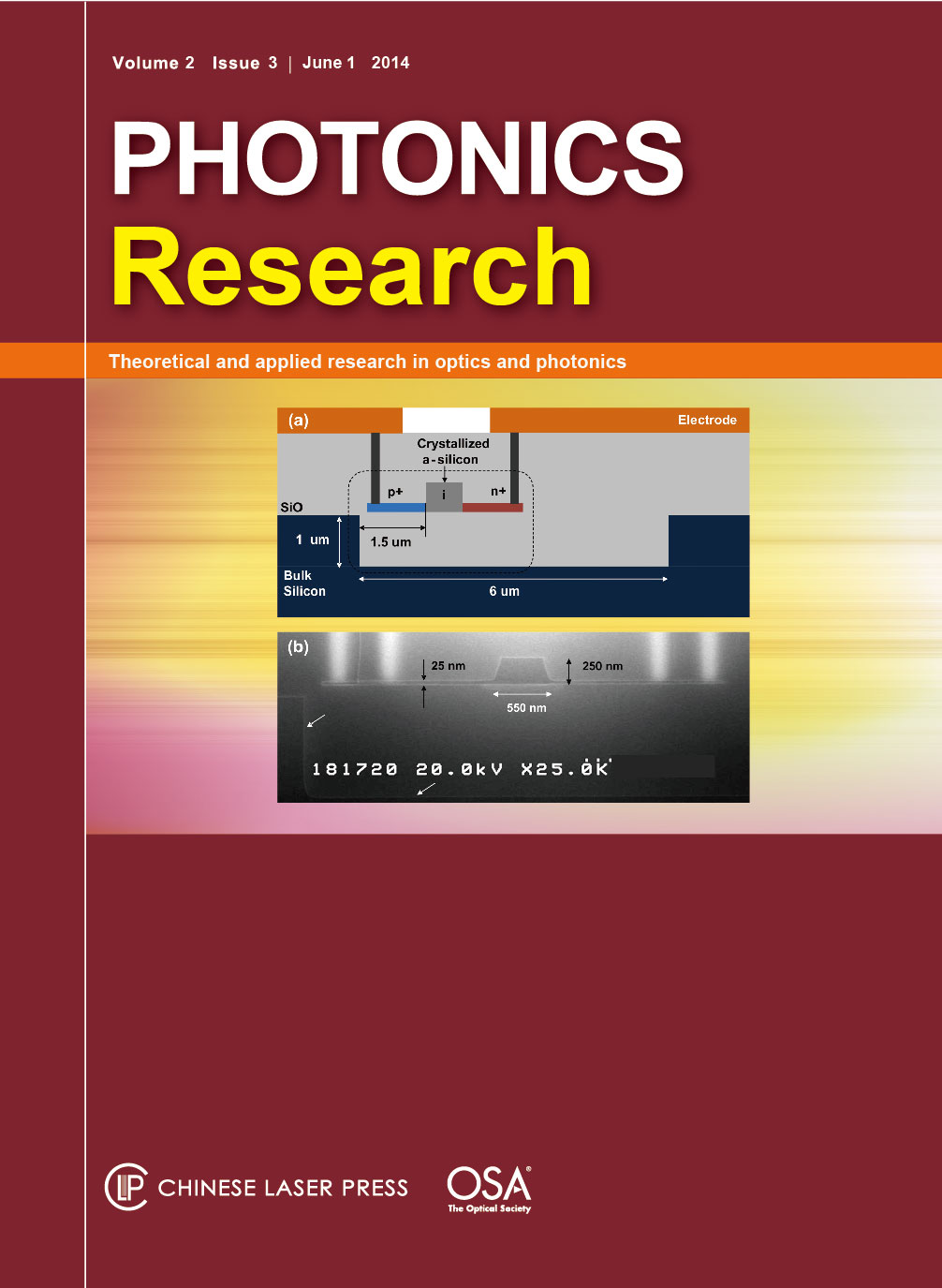
Hideo Isshiki, Fangli Jing, Takuya Sato, Takayuki Nakajima, and Tadamasa Kimura
ErxY2?xSiO5 and ErxYbyY2?x?ySiO5 crystalline thin films were investigated to apply to the high-gain media for silicon photonics. In addition to the sol–gel method, the directed self-assembly approach, using layer-by-layer deposition techniques, was also introduced to improve the crystallinity. The relaxation processes in Er ions were discussed to clarify the contribution of the energy transfer and cooperative upconversion. After optimization of the Er content, a Si photonic crystal slot ErxY2?xSiO5 waveguide amplifier was fabricated, and a 30 dB/cm modal gain was demonstrated. This achievement demonstrates the potential for compact and high optical gain devices on Si chips.
May. 09, 2014Vol. 2 Issue 3 03000A45 (2014)
Juanjuan Zheng, Peng Gao, Baoli Yao, Tong Ye, Ming Lei, Junwei Min, Dan Dan, Yanlong Yang, and and Shaohui Yan
When structured illumination is used in digital holographic microscopy (DHM), each direction of the illumination fringe is required to be shifted at least three times to perform the phase-shifting reconstruction. In this paper, we propose a scheme for spatial resolution enhancement of DHM by using the structured illumination but without phase shifting. The structured illuminations of different directions, which are generated by a spatial light modulator, illuminate the sample sequentially in the object plane. The formed object waves interfere with a reference wave in an off-axis configuration, and a CCD camera records the generated hologram. After the object waves are reconstructed numerically, a synthetic aperture is performed by an iterative algorithm to enhance the spatial resolution. The resolution improvement of the proposed method is proved and demonstrated by both simulation and experiment.
Jan. 01, 1900Vol. 2 Issue 3 03000087 (2014)
Pinghui Wu, Chenghua Sui, and and Wenhua Huang
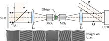
A quasi-Bessel beam (QBB) is suitable for laser ablation because it possesses a micrometer-sized focal spot and long depth of focus simultaneously. In this paper, the characterizations of QBBs formed by the ideal axicon and oblate-tip axicon are described. Strong on-axis intensity oscillations occur due to interference between the QBB and the refracted beam by the oblate tip. Using the axicon for laser ablation was theoretically investigated. Simple analytical formulas can be used to predict the required laser parameters, including the laser pulse energy, the generated fluence distributions, and the beam diameters.
Jan. 01, 1900Vol. 2 Issue 3 03000082 (2014)
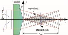
G. Baishali, V. Radhakrishna, V. Koushal, K. Rakhee, and and K. Rajanna
The detection efficiency of a gaseous photomultiplier depends on the photocathode quantum efficiency and the extraction efficiency of photoelectrons into the gas. In this paper we have studied the performance of an UV photon detector with P10 gas in which the extraction efficiency can reach values near to those in vacuum operated devices. Simulations have been done to compare the percentage of photoelectrons backscattered in P10 gas as well as in the widely used neon-based gas mixture. The performance study has been carried out using a single stage thick gas electron multiplier (THGEM). The electron pulses and electron spectrum are recorded under various operating conditions. Secondary effects prevailing in UV photon detectors like photon feedback are discussed and its effect on the electron spectrum under different operating conditions is analyzed.
Jan. 01, 1900Vol. 2 Issue 3 03000092 (2014)
Yutaka Urino, Tatsuya Usuki, Junichi Fujikata, Masashige Ishizaka, Koji Yamada, Tsuyoshi Horikawa, Takahiro Nakamura, and and Yasuhiko Arakawa
One of the most serious challenges facing exponential performance growth in the information industry is the bandwidth bottleneck in interchip interconnects. We propose a photonics–electronics convergence system in response to this issue. To demonstrate the feasibility of the system, we fabricated a silicon optical interposer integrated with arrayed laser diodes, spot-size converters, optical splitters, optical modulators, photodetectors, and optical waveguides on a single silicon substrate. Using this system, 20 Gbps error-free data links and a 30 Tbps/cm2 bandwidth density were achieved. This bandwidth density is sufficient to meet the interchip interconnect requirements for the late 2010s.
Jan. 01, 1900Vol. 2 Issue 3 030000A1 (2014)
Koji Yamada, Jurgen Michel, Marco Romagnoli, and and Hon Ki Tsang
Jan. 01, 1900Vol. 2 Issue 3 03000GP1 (2014)

David S. Sukhdeo, Donguk Nam, Ju-Hyung Kang, Mark L. Brongersma, and and Krishna C. Saraswat
We report uniaxial tensile strains up to 5.7% along in suspended germanium (Ge) wires on a silicon substrate, measured using Raman spectroscopy. This strain is sufficient to make Ge a direct bandgap semiconductor. Theoretical calculations show that a significant fraction of electrons remain in the indirect conduction valley despite the direct bandgap due to the much larger density of states; however, recombination can nevertheless be dominated by radiative direct bandgap transitions if defects are minimized. We then calculate the theoretical efficiency of direct bandgap Ge LEDs and lasers. These strained Ge wires represent a direct bandgap Group IV semiconductor integrated directly on a silicon platform.
Jan. 01, 1900Vol. 2 Issue 3 030000A8 (2014)
Hiroshi Fukuda, and and Kazumi Wada
We describe a polarization rotator based on a parallel-core structure consisting of a silicon nanowire waveguide and a silicon-nitride waveguide. The 60-μm-long rotator provides a polarization extinction ratio of more than 10 dB with excess loss of less than 1 dB. In addition, the extremely wide bandwidth of more than 150 nm expected from calculations is confirmed in experiments. A study of the fabrication tolerance of our rotator indicates that fabrication error of around 25 nm is allowable.
Jan. 01, 1900Vol. 2 Issue 3 03000A14 (2014)
Takanori Shimizu, Nobuaki Hatori, Makoto Okano, Masashige Ishizaka, Yutaka Urino, Tsuyoshi Yamamoto, Masahiko Mori, Takahiro Nakamura, and and Yashuhiko Arakawa
A hybrid integrated light source was developed with a configuration in which a laser diode (LD) array was mounted on a silicon optical waveguide platform for interchip optical interconnection. This integrated light source is composed of 13-channel stripes with a pitch of 20 or 30 μm. The output power of each LD in the 400 or 600-μm long LD array was over 40 mW at room temperature without cooling. An output power uniformity was 1.3 dB including an LD array power uniformity. The use of a SiON waveguide with a spot size converter resulted in an optical coupling loss of 1 dB between an LD and SiON waveguide. The integrated light source including 52 output ports demonstrated a reduction in the footprint per channel. We also demonstrated a light source with over 100 output ports in which the number of output ports is increased by using a waveguide splitter and multichip bonding. These integrated light sources are practical candidates for use with photonic integrated circuits for high-density optical interconnection.
Jan. 01, 1900Vol. 2 Issue 3 03000A19 (2014)
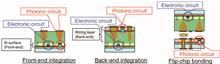
Hyunil Byun, Jinkwon Bok, Kwansik Cho, Keunyeong Cho, Hanmei Choi, Jinyong Choi, Sanghun Choi, Sangdeuk Han, Seokyong Hong, Seokhun Hyun, T. J. Jeong, Ho-Chul Ji, In-Sung Joe, Beomseok Kim, Donghyun Kim, Junghye Kim, Jeong-Kyoum Kim, Kiho Kim, Seong-Gu Kim, Duanhua Kong, Bongjin Kuh, Hyuckjoon Kwon, Beomsuk Lee, Hocheol Lee, Kwanghyun Lee, Shinyoung Lee, Kyoungwon Na, Jeongsik Nam, Amir Nejadmalayeri, Yongsang Park, Sunil Parmar, Junghyung Pyo, Dongjae Shin, Joonghan Shin, Yong-hwack Shin, Sung-Dong Suh, Honggoo Yoon, Yoondong Park, Junghwan Choi, Kyoung-Ho Ha, and and Gitae Jeong
We present photonics technology based on a bulk-Si substrate for cost-sensitive dynamic random-access memory (DRAM) optical interface application. We summarize the progress on passive and active photonic devices using a local-crystallized Si waveguide fabricated by solid phase epitaxy or laser-induced epitaxial growth on bulk-Si substrate. The process of integration of a photonic integrated circuit (IC) with an electronic IC is demonstrated using a 65 nm DRAM periphery process on 300 mm wafers to prove the possibility of seamless integration with various complementary metal-oxide-semiconductor devices. Using the bulk-Si photonic devices, we show the feasibility of high-speed multidrop interface: the Mach–Zehnder interferometer modulators and commercial photodetectors are used to demonstrate four-drop link operation at 10 Gb/s, and the transceiver chips with photonic die and electronic die work for the DDR3 DRAM interface at 1.6 Gb/s under a 1∶4 multidrop configuration.
Jan. 01, 1900Vol. 2 Issue 3 03000A25 (2014)
Michele Midrio, Paola Galli, Marco Romagnoli, Lionel C. Kimerling, and and Jurgen Michel
In this paper we report TE-mode phase modulation obtained by inducing a capacitive charge on graphene layers embedded in the core of a waveguide. There is a biasing regime in which graphene absorption is negligible but large index variations can be achieved with a voltage–length product as small as VπLπ~0.07 V cm for straight waveguides and VπLπ~0.0024 V cm for 12 μm radius microring resonators. This phase modulation device uniquely enables a small signal amplitude <1 V with a micrometer-sized footprint for compatibility with CMOS circuit integration. Examples of phase-induced changes are computed for straight waveguides and for microring resonators, showing the possibility of implementing several optoelectronic functionalities as modulators, tunable filters, and switches.
Jan. 01, 1900Vol. 2 Issue 3 03000A34 (2014)
Yunfei Fu, Tong Ye, Weijie Tang, and and Tao Chu
A silicon-on-insulator-based adiabatic waveguide taper with a high coupling efficiency and small footprint is presented. The taper was designed to reduce the incidence of mode conversion to higher-order and radiation modes inside the waveguide. In connecting a 0.5-μm-wide output waveguide and a 12-μm-wide input waveguide of a grating coupler, a compact 120-μm-long taper was demonstrated, achieving a transmission of 98.3%. Previously, this transmission level could only be achieved using a conventional linear taper with a length of more than 300 μm.
Jan. 01, 1900Vol. 2 Issue 3 03000A41 (2014)
© Copyright 2018-2021 | Chinese Laser Press.
All Rights Reserved 沪ICP备15018463号-20