


 View fulltext
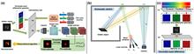
A method for three-dimensional vortex line visualization and chiral nanostructure fabrication by tightly focused multi-vortex beams via two-photon polymerization direct laser writing. It has wide applications in the fields of optical sensing, advanced functional devices, and information storage. See Mengdi Luo et al., pp. 70.
Fiber Optics and Optical Communications
Sergey Alyshev, Alexander Vakhrushev, Aleksandr Khegai, Elena Firstova, Konstantin Riumkin, Mikhail Melkumov, Lyudmila Iskhakova, Andrey Umnikov, and Sergei Firstov
Multi-wavelength-band transmission technology based on the exploitation of the extended spectral region is considered as a potential approach to increase the transmission capacity in the deployed fiber-optic communication infrastructure. The development of optical amplifiers operating in the O-, E-, S-, and U-telecom bands is an extremely important challenge for the successful implementation of this technology. Bismuth-doped fibers are of increasing interest as gain materials, which can be used to provide broadband amplification in the mentioned telecom bands. This is due to the ability of Bi ions incorporated into glass network to form bismuth active centers (BACs) with specific optical properties, which are primarily determined by the glass modifiers. In this work, the impact of the doping profiles of both Ge atoms as glass modifiers and Bi ions on the BACs formation is studied using a series of bismuth-doped fibers fabricated by the modified chemical vapor deposition (MCVD) technique. The Bi-to-BACs conversion efficiency in various spatial regions of the studied samples is presented. It is turned out that for high-Bi concentration regions, the conversion efficiency is very low (less than 10%). In addition, the relationship of the conversion efficiency to the distribution of Bi ions and/or Ge atoms is discussed. Finally, a continuous-wave laser at 1.46 μm with a record slope efficiency of 80% is demonstrated using a Bi-doped fiber with confined doping profile, where the Bi-to-BACs conversion efficiency is 35%. This paper provides new information which might help to facilitate understanding of the features of Bi-doped fibers and their potentially achievable characteristics.
Feb. 01, 2024Vol. 12 Issue 1 260 (2024)
Holography, Gratings, and Diffraction
Zhi-Dan Lei, Yi-Duo Xu, Cheng Lei, Yan Zhao, and Du Wang
Optical metasurfaces (OMs) offer unprecedented control over electromagnetic waves, enabling advanced optical multiplexing. The emergence of deep learning has opened new avenues for designing OMs. However, existing deep learning methods for OMs primarily focus on forward design, which limits their design capabilities, lacks global optimization, and relies on prior knowledge. Additionally, most OMs are static, with fixed functionalities once processed. To overcome these limitations, we propose an inverse design deep learning method for dynamic OMs. Our approach comprises a forward prediction network and an inverse retrieval network. The forward prediction network establishes a mapping between meta-unit structure parameters and reflectance spectra. The inverse retrieval network generates a library of meta-unit structure parameters based on target requirements, enabling end-to-end design of OMs. By incorporating the dynamic tunability of the phase change material Sb2Te3 with inverse design deep learning, we achieve the design and verification of dynamic multifunctional OMs. Our results demonstrate OMs with multiple information channels and encryption capabilities that can realize multiple physical field optical modulation functions. When Sb2Te3 is in the amorphous state, near-field nano-printing based on meta-unit amplitude modulation is achieved for X-polarized incident light, while holographic imaging based on meta-unit phase modulation is realized for circularly polarized light. In the crystalline state, the encrypted information remains secure even with the correct polarization input, achieving double encryption. This research points towards ultra-compact, high-capacity, and highly secure information storage approaches.
Dec. 22, 2023Vol. 12 Issue 1 123 (2024)
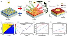
Image Processing and Image Analysis
Ze-Hao Wang, Long-Kun Shan, Tong-Tian Weng, Tian-Long Chen, Xiang-Dong Chen, Zhang-Yang Wang, Guang-Can Guo, and Fang-Wen Sun
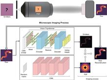
The optical microscopy image plays an important role in scientific research through the direct visualization of the nanoworld, where the imaging mechanism is described as the convolution of the point spread function (PSF) and emitters. Based on a priori knowledge of the PSF or equivalent PSF, it is possible to achieve more precise exploration of the nanoworld. However, it is an outstanding challenge to directly extract the PSF from microscopy images. Here, with the help of self-supervised learning, we propose a physics-informed masked autoencoder (PiMAE) that enables a learnable estimation of the PSF and emitters directly from the raw microscopy images. We demonstrate our method in synthetic data and real-world experiments with significant accuracy and noise robustness. PiMAE outperforms DeepSTORM and the Richardson–Lucy algorithm in synthetic data tasks with an average improvement of 19.6% and 50.7% (35 tasks), respectively, as measured by the normalized root mean square error (NRMSE) metric. This is achieved without prior knowledge of the PSF, in contrast to the supervised approach used by DeepSTORM and the known PSF assumption in the Richardson–Lucy algorithm. Our method, PiMAE, provides a feasible scheme for achieving the hidden imaging mechanism in optical microscopy and has the potential to learn hidden mechanisms in many more systems.
Dec. 08, 2023Vol. 12 Issue 1 7 (2024)
Yaoming Bian, Fei Wang, Yuanzhe Wang, Zhenfeng Fu, Haishan Liu, Haiming Yuan, and Guohai Situ
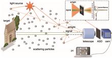
Imaging through non-static and optically thick scattering media such as dense fog, heavy smoke, and turbid water is crucial in various applications. However, most existing methods rely on either active and coherent light illumination, or image priors, preventing their application in situations where only passive illumination is possible. In this study we present a universal passive method for imaging through dense scattering media that does not depend on any prior information. Combining the selection of small-angle components out of the incoming information-carrying scattering light and image enhancement algorithm that incorporates time-domain minimum filtering and denoising, we show that the proposed method can dramatically improve the signal-to-interference ratio and contrast of the raw camera image in outfield experiments.
Dec. 22, 2023Vol. 12 Issue 1 134 (2024)
Imaging Systems, Microscopy, and Displays
Single-shot non-line-of-sight imaging based on chromato-axial differential correlographySpotlight on Optics
Lingfeng Liu, Shuo Zhu, Wenjun Zhang, Lianfa Bai, Enlai Guo, and Jing Han
Non-line-of-sight (NLOS) imaging is a challenging task aimed at reconstructing objects outside the direct view of the observer. Nevertheless, traditional NLOS imaging methods typically rely on intricate and costly equipment to scan and sample the hidden object. These methods often suffer from restricted imaging resolution and require high system stability. Herein, we propose a single-shot high-resolution NLOS imaging method via chromato-axial differential correlography, which adopts low-cost continuous-wave lasers and a conventional camera. By leveraging the uncorrelated laser speckle patterns along the chromato-axis, this method can reconstruct hidden objects of diverse complexity using only one exposure measurement. The achieved background stability through single-shot acquisition, along with the inherent information redundancy in the chromato-axial differential speckles, enhances the robustness of the system against vibration and colored stain interference. This approach overcomes the limitations of conventional methods by simplifying the sampling process, improving system stability, and achieving enhanced imaging resolution using available equipment. This work serves as a valuable reference for the real-time development and practical implementation of NLOS imaging.
Dec. 21, 2023Vol. 12 Issue 1 106 (2024)
Instrumentation and Measurements
Yuan Wang, Pedro Tovar, Juntong Yang, Liang Chen, and Xiaoyi Bao
A Brillouin dynamic grating (BDG) can be used for distributed birefringence measurement in optical fibers, offering high sensitivity and spatial resolution for sensing applications. However, it is quite a challenge to simultaneously achieve dynamic measurements with both high accuracy and high spatial resolution. In this work, we propose a sensing mechanism to achieve distributed phase-matching measurement using a chirped pulse as a probe signal. In BDG reflection, the peak reflection corresponds to the highest four-wave mixing (FWM) conversion efficiency, and it requires the Brillouin frequency in the fast and slow axes to be equal, which is called the phase-matching condition. This condition changes at different fiber positions, which requires a range of frequency injection for the probe wave. The proposed method uses a chirped pulse as a probe wave to cover this frequency range associated with distributed birefringence inhomogeneity. This allows us to detect distributed phase matching for birefringence changes that are introduced by temperature and strain variations. Thanks to the single shot and direct time delay measurement capability, the acquisition rate in our system is only limited by the fiber length. Notably, unlike conventional BDG spectrum recovery-based systems, the spatial resolution here is determined by both the frequency chirping rate of the probe pulse and the birefringence profile of the fiber. In the experiments, an acquisition rate of 1 kHz (up to fiber length limits) and a spatial resolution of 10 cm using a 20 ns probe pulse width are achieved. The minimum detectable temperature and strain variation are 5.6 mK and 0.37 με along a 2 km long polarization-maintaining fiber (PMF).
Dec. 22, 2023Vol. 12 Issue 1 141 (2024)

Shengyang Wu, Benli Yu, and Lei Zhang
An imperfect propagation environment or optical system would introduce wavefront aberrations to vortex beams. The phase aberrations and orbital angular momentum in a vortex beam are proved to be mutually restrictive in parameter measurement. Aberrations make traditional topological charge (TC) probing methods ineffective while the phase singularity makes phase retrieval difficult due to the aliasing between the wrapped phase jump and the vortex phase jump. An interactive probing method is proposed to make measurements of the aberrated phase and orbital angular momentum in a vortex beam assist rather than hinder each other. The phase unwrapping is liberated from the phase singularity by an annular shearing interference technique while the TC value is determined by a Moiré technique immune to aberrations. Simulation and experimental results proving the method effective are presented. It is of great significance to judge the characteristics of vortex beams passing through non-ideal environments and optical systems.
Dec. 22, 2023Vol. 12 Issue 1 172 (2024)
Integrated Optics
Yuan Shen, Xiaoqian Shu, Lingmei Ma, Shaoliang Yu, Gengxin Chen, Liu Liu, Renyou Ge, Bigeng Chen, and Yunjiang Rao
We experimentally demonstrate ultra-high extinction ratio (ER) optical pulse modulation with an electro-optical modulator (EOM) on thin film lithium niobate (TFLN) and its application for fiber optic distributed acoustic sensing (DAS). An interface carrier effect leading to a relaxation-tail response of TFLN EOM is discovered, which can be well addressed by a small compensation component following the main driving signal. An ultra-high ER > 50 dB is achieved by canceling out the tailed response during pulse modulation using the EOM based on a cascaded Mach–Zehnder interferometer (MZI) structure. The modulated optical pulses are then utilized as a probe light for a DAS system, showing a sensitivity up to -62.9 dB ⋅ rad/Hz2 (7 pε/√Hz) for 2-km single-mode sensing fiber. Spatial crosstalk suppression of 24.9 dB along the fiber is also obtained when the ER is improved from 20 dB to 50 dB, clearly revealing its importance to the sensing performance.
Dec. 14, 2023Vol. 12 Issue 1 40 (2024)
Andrea Zazzi, Arka Dipta Das, Lukas Hüssen, Renato Negra, and Jeremy Witzens
We propose a new signaling scheme for on-chip optical-electrical-optical artificial neural networks that utilizes orthogonal delay-division multiplexing and pilot-tone-based self-homodyne detection. This scheme offers a more efficient scaling of the optical power budget with increasing network complexity. Our simulations, based on 220 nm silicon-on-insulator silicon photonics technology, suggest that the network can support 31×31 neurons, with 961 links and freely programmable weights, using a single 500 mW optical comb and a signal-to-noise ratio of 21.3 dB per neuron. Moreover, it features a low sensitivity to temperature fluctuations, ensuring that it can be operated outside of a laboratory environment. We demonstrate the network’s effectiveness in nonlinear equalization tasks by training it to equalize a time-interleaved analog-to-digital converter (ADC) architecture, achieving an effective number of bits over 4 over the entire 75 GHz ADC bandwidth. We anticipate that this network architecture will enable broadband and low latency nonlinear signal processing in practical settings such as ultra-broadband data converters and real-time control systems.
Dec. 21, 2023Vol. 12 Issue 1 85 (2024)
Jianing Wang, Xi Wang, Yihang Li, Yanfu Yang, Qinghai Song, and Ke Xu
Recently, the emerging 2 μm waveband has gained increasing interest due to its great potential for a wide scope of applications. Compared with the existing optical communication windows at shorter wavelengths, it also offers distinct advantages of lower nonlinear absorption, better fabrication tolerance, and larger free carrier plasma effects for silicon photonics, which has been a proven device technology. While much progress has been witnessed for silicon photonics at the 2 μm waveband, the primary challenge still exists for on-chip detectors. Despite the maturity and compatibility of the waveguide coupled photodetectors made of germanium, the 2 μm regime is far beyond its cutoff wavelength. In this work, we demonstrate an efficient and high-speed on-chip waveguide-coupled germanium photodetector operating at the 2 μm waveband. The weak sub-bandgap absorption of epitaxial germanium is greatly enhanced by a lateral separation absorption charge multiplication structure. The detector is fabricated by the standard process offered by a commercial foundry. The device has a benchmark performance with responsivity of 1.05 A/W and 3 dB bandwidth of 7.12 GHz, which is able to receive high-speed signals with up to 20 Gbit/s data rate. The availability of such an efficient and fast on-chip detector circumvents the barriers between silicon photonic integrated circuits and the potential applications at the 2 μm waveband.
Dec. 21, 2023Vol. 12 Issue 1 115 (2024)
Runlin Miao, Ke Yin, Chao Zhou, Chenxi Zhang, Zhuopei Yu, Xin Zheng, and Tian Jiang
Microcombs have enabled a host of cutting-edge applications from metrology to communications that have garnered significant attention in the last decade. Nevertheless, due to the thermal instability of the microresonator, additional control devices like auxiliary lasers are indispensable for single-soliton generation in some scenarios. Specifically, the increased system complexity would be too overwhelming for dual-microcomb generation. Here, we put forward a novel approach to mitigate the thermal instability and generate the dual-microcomb using a compact system. This process is akin to mode-division multiplexing, as the dual-microcombs are generated by pumping the dual-mode of a single Si3N4 microresonator with a continuous-wave laser. Both numerical simulations and experimental measurements indicate that this innovative technique could offer a straightforward way to enlarge the soliton existence range, allowing entry into the multistability regime and triggering another microcomb alongside the main soliton pulse. This outcome not only shines new light on the interaction mechanism of microresonator modes but also provides an avenue for the development of dual-microcomb-based ranging and low phase noise microwave generation.
Dec. 22, 2023Vol. 12 Issue 1 163 (2024)
Lasers and Laser Optics
Changsheng Zheng, Tianyi Du, Lei Zhu, Zhanxin Wang, Kangzhen Tian, Yongguang Zhao, Zhiyong Yang, Haohai Yu, and Valentin Petrov
Spatially twisted light with femtosecond temporal structure is of particular interest in strong-field physics and light–matter interactions. However, present femtosecond vortex sources exhibit limited power handling capabilities, and their amplification remains an ongoing challenge particularly for high-order orbital angular momentum (OAM) states due to several inherent technical difficulties. Here, we exploit a straightforward approach to directly amplify a femtosecond optical vortex (FOV, OAM=-8ℏ) by using a two-stage single-crystal fiber (SCF) amplifier system without pulse stretching and compression in the time domain, delivering 23-W, 163-fs pulses at a repetition rate of 1 MHz. The spatial and temporal features are well-conserved during the amplification, as well as the high modal purity (>96%). The results indicate that the multi-stage SCF amplifier system is particularly suited for direct amplification of high-order FOVs. The generated high-power femtosecond OAM laser beams are expected to help reveal complex physical phenomena in light–matter interactions and pave the way for practical applications in attoscience, laser plasma acceleration, and high-dimension micromachining.
Dec. 14, 2023Vol. 12 Issue 1 27 (2024)
Nanophotonics and Photonic Crystals
Mengdi Luo, Jisen Wen, Pengcheng Ma, Qiuyuan Sun, Xianmeng Xia, Gangyao Zhan, Zhenyao Yang, Liang Xu, Dazhao Zhu, Cuifang Kuang, and Xu Liu
Optical singularity is pivotal in nature and has attracted wide interest from many disciplines nowadays, including optical communication, quantum optics, and biomedical imaging. Visualizing vortex lines formed by phase singularities and fabricating chiral nanostructures using the evolution of vortex lines are of great significance. In this paper, we introduce a promising method based on two-photon polymerization direct laser writing (2PP-DLW) to record the morphology of vortex lines generated by tightly focused multi-vortex beams (MVBs) at the nanoscale. Due to Gouy phase, the singularities of the MVBs rotate around the optical axis and move towards each other when approaching the focal plane. The propagation dynamics of vortex lines are recorded by 2PP-DLW, which explicitly exhibits the evolution of the phase singularities. Additionally, the MVBs are employed to fabricate stable three-dimensional chiral nanostructures due to the spiral-forward property of the vortex line. Because of the obvious chiral features of the manufactured nanostructures, a strong vortical dichroism is observed when excited by the light carrying orbital angular momentum. A number of applications can be envisioned with these chiral nanostructures, such as optical sensing, chiral separation, and information storage.
Dec. 21, 2023Vol. 12 Issue 1 70 (2024)
Yuxin Yang, Jiaxin Gao, Hao Wu, Zhanke Zhou, Liu Yang, Xin Guo, Pan Wang, and Limin Tong
An optical field with sub-nm confinement is essential for exploring atomic- or molecular-level light-matter interaction. While such fields demonstrated so far have typically point-like cross-sections, an optical field having a higher-dimensional cross-section may offer higher flexibility and/or efficiency in applications. Here, we propose generating a nanoscale blade-like optical field in a coupled nanofiber pair (CNP) with a 1-nm-width central slit. Based on a strong mode coupling-enabled slit waveguide mode, a sub-nm-thickness blade-like optical field can be generated with a cross-section down to ∼0.28 nm×38 nm at 1550 nm wavelength (i.e., a thickness of ∼λ0/5000) and a peak-to-background intensity ratio (PBR) higher than 20 dB. The slit waveguide mode of the CNP can be launched from one of the two nanofibers that are connected to a standard optical fiber via an adiabatical fiber taper, in which a fundamental waveguide mode of the fiber can be converted into a high-purity slit mode with high efficiency (>98%) within a CNP length of less than 10 μm at 1550 nm wavelength. The wavelength-dependent behaviors and group velocity dispersion in mode converting processes are also investigated, showing that such a CNP-based design is also suitable for broadband and ultrafast pulsed operation. Our results may open up new opportunities for studying light-matter interaction down to the sub-nm scale, as well as for exploring ultra-high-resolution optical technology ranging from super-resolution nanoscopy to chemical bond manipulation.
Dec. 22, 2023Vol. 12 Issue 1 154 (2024)
Physical Optics
Zhuoyi Wang, Xingyuan Lu, Jianbo Gao, Xuechun Zhao, Qiwen Zhan, Yangjian Cai, and Chengliang Zhao
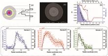
Fractional vortex beams exhibit a higher degree of modulation dimensions than conventional vortices, thus inheriting superior anti-turbulent transmission properties through the incorporation of additional coherence modulation. However, aliasing the mixed modes induced by coherence degradation makes the quantitative measurement of the topological charge in fractional vortex beams challenging. In this study, a coherence phase spectrum was introduced, and experimental demonstrations to quantitatively determine the fractional topological charge of partially coherent fractional vortex beams were performed. By leveraging the four-dimensional measurement of a partially coherent light field, the source coherence function was inversely reconstructed, and fractional topological charges were determined with high precision by extracting the phase spectrum of the coherence function. Laguerre–Gaussian, elliptical Gaussian, and plane-wave-fraction vortex beams with various degrees of coherence were used to demonstrate measurement precision. The proposed method is applicable to X-rays and electron vortices. It has potential applications in optical encryption, high-capacity optical communication, and quantum entanglement.
Dec. 14, 2023Vol. 12 Issue 1 33 (2024)
Xiaoqiuyan Zhang, Tianyu Zhang, Zhuocheng Zhang, Xingxing Xu, Diwei Liu, Zhaoyun Duan, Yanyu Wei, Yubin Gong, Liang Jie Wong, and Min Hu
The interaction between electrons and matter is an effective means of light emission, through mechanisms including Cherenkov radiation and Smith–Purcell radiation (SPR). In this study, we show that the superlight inverse Doppler effects can be realized in reverse Smith–Purcell radiation excited by a free electron beam with a homogeneous substrate. In particular, we find that two types of anomalous SPR exist in the homogenous substrate: special SPR and reverse SPR. Our results reveal that the electron velocity can be tuned to simultaneously excite different combinations of normal SPR, special SPR, and reverse SPR. The proposed manifold light radiation mechanism can offer greater versatility in controlling and shaping SPR.
Dec. 21, 2023Vol. 12 Issue 1 78 (2024)
Silicon Photonics
Yang Shi, Xiang Li, Mingjie Zou, Yu Yu, and Xinliang Zhang
High-performance germanium photodiodes are crucial components in silicon photonic integrated circuits for large-capacity data communication. However, the bandwidths of most germanium photodiodes are limited by the intractable resistance–capacitance parasitic effect. Here, we introduce a unique U-shaped electrode to alleviate this issue, reducing the parasitic effect by 36% without compromising any other performance. Experimentally, a large bandwidth of 103 GHz, an optical responsivity of 0.95 A/W at 1550 nm, and a dark current as low as 1.3 nA are achieved, leading to a record high specific detectivity. This is the first breakthrough to 100 GHz bandwidth among all vertical germanium photodiodes, to the best of our knowledge. Open eye diagrams of 120 Gb/s on-off keying and 200 Gb/s four-level pulse amplitude signals are well received. This work provides a promising solution for chip-based ultra-fast photodetection.
Dec. 08, 2023Vol. 12 Issue 1 1 (2024)
Jonathan Peltier, Weiwei Zhang, Leopold Virot, Christian Lafforgue, Lucas Deniel, Delphine Marris-Morini, Guy Aubin, Farah Amar, Denh Tran, Xingzhao Yan, Callum G. Littlejohns, Carlos Alonso-Ramos, Ke Li, David J. Thomson, Graham Reed, and Laurent Vivien
Silicon-based electro-optic modulators contribute to easing the integration of high-speed and low-power consumption circuits for classical optical communications and data computations. Beyond the plasma dispersion modulation, an alternative solution in silicon is to exploit the DC Kerr effect, which generates an equivalent linear electro-optical effect enabled by applying a large DC electric field. Although some theoretical and experimental studies have shown its existence in silicon, limited contributions relative to plasma dispersion have been achieved in high-speed modulation so far. This paper presents high-speed optical modulation based on the DC Kerr effect in silicon PIN waveguides. The contributions of both plasma dispersion and Kerr effects have been analyzed in different waveguide configurations, and we demonstrated that the Kerr induced modulation is dominant when a high external DC electric field is applied in PIN waveguides. High-speed optical modulation response is analyzed, and eye diagrams up to 80 Gbit/s in NRZ format are obtained under a d.c. voltage of 30 V. This work paves the way to exploit the Kerr effect to generate high-speed Pockels-like optical modulation.
Dec. 14, 2023Vol. 12 Issue 1 51 (2024)
Surface Optics and Plasmonics
Bowen Zeng, Chenxia Li, Bo Fang, Zhi Hong, and Xufeng Jing
Programmable hyper-coded holography has the advantage of being programmable as well as being flexibly modifiable. Digitally coded metamaterials with excellent electromagnetic modulation capability and the ability to control the phase to modulate the spatial radiation field through external excitation in the form of switching can be used to realize low-cost digital arrays. We design a 1-bit encoded programmable metasurface, which is electrically connected to control the PIN diode in the switching state and to switch the condition of each metasurface cell between “0” and “1.” Using the designed programmable metasurface, we can randomly encode the cell structure to realize single-focus focusing, multi-focusing, and simple holographic letter imaging. Based on the nonlinear holographic model, we employ the Gerchberg-Saxton improvement algorithm to modulate the energy distribution at the focus by adjusting the phase distribution. Importantly, we introduce the Fourier convolution principle to regulate the holographic imaging focus flexibly.
Dec. 21, 2023Vol. 12 Issue 1 61 (2024)
© Copyright 2018-2021 | Chinese Laser Press.
All Rights Reserved 沪ICP备15018463号-20