


Please enter the answer below before you can view the full text.
9-8=
Guest Editors:
Qing Zhang,
Peking University, China (Lead editor)
Carole Diederichs,
Sorbonne University, France
Qihua Xiong,
Nanyang Technological University, Singapore
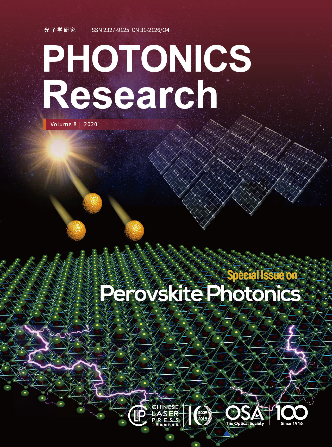
On the Cover for this virtual special issue
Large area perovskite solar cells: the way for application. See Yang Zhao et al., page 070000A1.
Halide perovskite semiconductors have emerged as promising candidates for the next-generation low-energy consumption, high-flexibility photonics and optoelectronic devices thanks to their superior optical and excitonic properties as well as fabrication convenience. This special issue, including three review papers and six original research papers, focuses on the studies of both fundamentals and applications of perovskite photonics, covering materials, excitonic properties, nonlinear optics, strong light–matter interactions, and optoelectronic devices.
The record power conversion efficiency of small-area perovskite solar cells has impressively exceeded 25%. For commercial application, a large-area device is the necessary next step. Recently, significant progress has been achieved in fabricating efficient large-area perovskite solar cells. In this review, we will summarize recent achievements in large-area perovskite solar cells including the deposition methods as well as growth control of the large-area, high-quality perovskite layer and also the charge transport layer. Finally, we will give our insight into large-area perovskite solar cells.
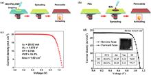
Hybrid perovskite materials are widely researched due to their high absorptivity, inexpensive synthesis, and promise in photovoltaic devices. These materials are also of interest as highly sensitive photodetectors. In this study, their potential for use in visible light communication is explored in a configuration that allows for simultaneous energy and data harvesting. Using a triple-cation material and appropriate device design, a new record data rate for perovskite photodetectors of 56 Mbps and power conversion efficiencies above 20% under white LED illumination are achieved. With this device design, the −3 dB bandwidth is increased by minimizing the dominating time constant of the system. This correlation between the bandwidth and time constant is proved using measurements of time-resolved photoluminescence, transient photovoltage, and device resistance.
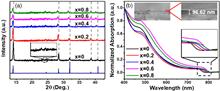
Metal halide perovskite materials have been widely studied recently due to their excellent optoelectronic properties. Among these materials, organic-inorganic hybrid perovskites have attracted much attention because of their relatively soft framework, which makes them more suitable for nonlinear optical (NLO) applications. However, there is rare physical mechanism study on the coexistence of two-photon absorption (TPA) and saturable absorption (SA) in organic-inorganic hybrid perovskite materials. To clarify this issue, the NLO properties of mixed cation perovskite MA1-xFAxPbI3 [MA=CH3NH3,FA=CH(NH2)2, x=0, 0.2, 0.4, 0.6, and 0.8] thin films are investigated in this paper. Based on the nonlinear transmittance and femtosecond-transient absorption spectrum measurements, it is found that the MA1-xFAxPbI3 materials exhibit NLO behavior dependent on excitation intensity. The TPA coefficient of MA1-xFAxPbI3 decreases with the increase of formamidinium (FA) content, while the relevant saturable intensity increases. In addition, it is revealed that the linear absorption process from valence band 2 to valance band 1 still exists even under a very low excitation intensity. With the increase of excitation intensity, the light transmittance at 1300 nm decreases first and then increases sharply, which also supports the explanation for the coexistence of TPA and SA. It is expected that our findings will promote the application of perovskite materials in nonlinear optoelectronic devices.
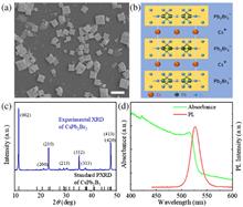
In recent years, halide perovskite nanostructures have had great advances and have opened up a bright future for micro/nanolasers. However, upconversion lasing by two-photon excitation with mode selection and high quality factor in one device is still rarely reported. Herein, two lasing modes are demonstrated in the all-inorganic perovskite CsPb2Br5 microplates with subwavelength thickness and uniform square shape. The net optical gain is quickly established in less than 1 ps and persists more than 30 ps, revealed by ultrafast transient absorption spectroscopy. The temperature-dependent low-threshold amplified spontaneous emission confirms the net gain for stimulated emission with a high characteristic temperature of 403 K, far surpassing the all-inorganic CsPbBr3 semiconductor gain media. Remarkably, upconversion lasing based on two kinds of microcavity effects, Fabry–Pérot and whispering-gallery modes, from the microplates at room temperature is successfully achieved with a low threshold operating in multi- or single-mode, respectively. Surprisingly, the quality factor (~3551) is among the best values obtained from perovskite micro/nanoplate upconversion lasers without an external cavity. Moreover, the highly stable chromaticity with color drift only less than 0.1 nm also outbalances the all-inorganic CsPbBr3 ones. These superior performances of CsPb2Br5 microplate lasing with a facile solution synthesis procedure will offer a feasible structure to fabricate specific functionalities for high-performance frequency upconversion micro/nanoscale photonic integrated devices.
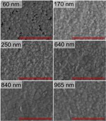
Modifying the surface of poly[bis(4-phenyl)(2,4,6-trimethylphenyl)amine] (PTAA) with toluene during the high-speed spin-coating process of dimethylformamide considerably improves the wettability and morphology of PTAA and results in improvement of the crystallinity and absorption of perovskite film. The hole mobility and ohm contact have also been improved accordingly. Combined with these improved parameters, inverted perovskite solar cells with high efficiency of 19.13% and long-term stability could be achieved, which are much better than those with untreated PTAA. Importantly, our devices can keep 88.4% of the initial power conversion efficiency after 30 days of storage in ambient air.
High magnetic field spectroscopy has been performed on lead chloride-based perovskite, a material that attracts significant interest for photovoltaic and photonic applications within the past decades. Optical properties being mainly driven by the exciton states, we have measured the fundamental parameters, such as the exciton binding energy, effective mass, and dielectric constant. Among the inorganic halide perovskites, CsPbCl3 owns the largest exciton binding energy and effective mass. This blue emitting compound has also been compared with lower band gap energy perovskites and other semiconducting phases, showing comparable band gap dependences for binding energy and Bohr radius.
Halide perovskites, such as methylammonium lead halide perovskites (MAPbX3, X=I, Br, and Cl), are emerging as promising candidates for a wide range of optoelectronic applications, including solar cells, light-emitting diodes, and photodetectors, due to their superior optoelectronic properties. All-inorganic lead halide perovskites CsPbX3 are attracting a lot of attention because replacing the organic cations with Cs+ enhances the stability, and its halide-mixing derivatives offer broad bandgap tunability covering nearly the entire visible spectrum. However, there is evidence suggesting that the optical properties of mixed-halide perovskites are influenced by phase segregation under external stimuli, especially illumination, which may negatively impact the performance of optoelectronic devices. It is reported that the mixed-halide perovskites in forms of thin films and nanocrystals are segregated into a low-bandgap I-rich phase and a high-bandgap Br-rich phase. Herein, we present a critical review on the synthesis and basic properties of all-inorganic perovskites, phase-segregation phenomena, plausible mechanisms, and methods to mitigate phase segregation, providing insights on advancing mixed-halide perovskite optoelectronics with reliable performance.
Two-dimensional (2D) perovskites are hybrid layered materials in which the inorganic lattice of an octahedron is sandwiched by organic layers. They behave as a quantum-well structure exhibiting large exciton binding energy and high emission efficiency, which is excellent for photonic applications. Hence, the cavity modulation and cavity devices of 2D perovskites are widely investigated. In this review, we summarize the rich photophysics, synthetic methods of different cavity structures, and the cavity-based applications of 2D perovskites. We highlight the strong exciton–photon coupling and photonic lasing obtained in different cavity structures. In addition, functional optoelectronic devices using cavity structures of 2D perovskites are also reviewed.
We present theoretically the formation of exciton–photon polaritons and exciton-surface plasmon polaritons in a perovskite-based subwavelength lattice on the metallic plane. It is shown that the later polaritons will be achieved as the perovskite layer is ultra-thin (<50 nm), while the co-existence of both polaritons will dominate, as the thickness of the perovskite metasurface approaches wavelength-scale. In the two cases, the lower polaritonic branches consist of dark and bright modes corresponding to infinite and finite radiative quality factors, respectively. Another salient property in this work is that it allows one to obtain exceptional points (EPs) in momentum space with a four-fold enhancement of local density of states through engineering the perovskite metasurface. Our findings show that the perovskite metasurface is an attractive and rich platform to make polaritonic devices, even with the presence of a lossy metallic layer.