


Abstract
Solution-processed metal halide perovskites are widely studied for their potential in high-efficiency light-emitting diodes, yet they are facing several challenges like insufficient brightness, short operational lifetimes, and reduced power conversion efficiency under practical operation conditions. Here, we develop an interfacial amidation reaction on sacrificial ZnO substrates to produce perovskite films with low trap density (1.2 × 1010 cm−3), and implement a device structure featuring a mono-molecular hole-injection layer and an all-inorganic bi-layered electron-injection layer. This design leads to green perovskite light-emitting diodes with a brightness of ~ 312,000 cd m−2, a half-lifetime of 350 h at 1000 cd m−2, and a power conversion efficiency of 15.6% at a current density of 300 mA cm−2. Furthermore, the perovskite films show a low amplified spontaneous emission threshold of 13 μJ cm−2. Thus, our approach significantly advances the performance of green perovskite light-emitting diodes and opens up an avenue toward perovskite-based electrically pumped lasers.
Introduction
Solution-processed metal halide perovskites, known for their superior luminescence properties such as pure and tuneable light emission, high photoluminescence quantum yields (PLQYs), and favourable charge transport properties, have emerged as promising materials for energy-efficient light-emitting diodes (LEDs) that potentially offer high brightness at low driving voltages, thus achieving high power conversion efficiencies (PCE)1,2,3,4,5,6,7,8,9. PCE value quantifies how effectively the input electric power is converted into light output (see Supplementary Note 1 for detailed calculations), making it a more crucial metric than the commonly reported external quantum efficiencies (EQEs). Since the pioneering demonstration of room-temperature electroluminescence (EL) from metal halide perovskites in 20141,10, significant progress has been made on perovskite LEDs. Research has focused on improvements of the light-emissive layers through various strategies such as additive engineering4,11,12,13, dimensionality tailoring14,15, manipulation of precursor compositions16,17, and post-treatment of perovskite films6,18. Additionally, the introduction of hole-injection layers (HILs) using organic polymers and electron-injection layers (EILs) employing small organic molecules or ZnO nanocrystals has further boosted the performance of such devices3,4. These advancements have culminated in a recent realization of near-infrared, red, green, and blue perovskite LEDs with EQEs exceeding 20%6,7,19,20,21,22, with values approaching theoretical limits dictated by light out-coupling efficiencies. However, the incorporation of additives or polymers in perovskite films and the use of organic charge-injection layers (CILs) characterized by relatively low carrier mobility often impede the charge transport, necessitating higher driving voltages for optimal device operation, which in turn leads to reduced PCEs3,4. Lower PCE values indicate increased ohmic and non-radiative losses, resulting in heat generation that adversely affects LED operational stability5,23.
Previous studies have indicated that perovskite LEDs employing an all-inorganic device architecture, where perovskite layers are sandwiched between HILs based on indium tin oxide (ITO) or NiOx, and EILs based on ZnO, tend to exhibit reduced operational voltages24,25. However, such architectures often suffer from low-quality of the perovskite films deposited on those oxide substrates, and from severe degradation of perovskite films caused by polar solvents during the ZnO deposition process25. Consequently, the efficiency and stability of all-inorganic architecture perovskite LEDs lag behind the state-of-the-art devices utilizing organic-based CILs (see Supplementary Table 1).
Herein, we report bright and stable green perovskite LEDs with high PCEs, achieved by a combination of optimized fabrication techniques and device architecture. We introduce an interfacial amidation reaction between a ZnO sacrificial layer and a perovskite precursor film comprising formamidinium bromide (FABr), lead bromide (PbBr2), and a dicarboxylic acid. We reveal that the complete consumption of the sacrificial ZnO layer in the amidation process leads to an exceptionally low trap density of 1.2 × 1010 cm−3 for the resulting optimized formamidinium lead bromide (FAPbBr3) films. Furthermore, we designed an all-inorganic device architecture where the FAPbBr3 films are sandwiched between an ITO electrode modified with a functional self-assembled monolayer (SAM) as HIL and a dual-layer EIL composed of thiol-modified ZnO (ZnO-S) layer topped with atomic layer deposited ZnO (ALD-ZnO) layer. This device configuration ensures efficient electron transport while minimizing interfacial emission quenching, enabling the perovskite LEDs to achieve high brightness, prolonged operational lifetime, and high PCEs simultaneously. Moreover, the precise control over the interfacial amidation reaction leads to FAPbBr3 films with a low amplified spontaneous emission (ASE) threshold of 13 μJ cm−2, further demonstrating the potential of our approach for next-generation optoelectronic applications beyond LEDs, such as lasers.
Results
Interfacial amidation reaction for perovskite films
Figure 1a depicts the fabrication and the film formation process of 3D FAPbBr3 perovskite. A precursor solution (9 wt.%) containing PbBr2:FABr:pimelic acid (PAC) with a molar ratio of 2.8:1:0.6 was spin-coated onto a 10 nm ZnO substrate, followed by thermal annealing to promote the amidation reaction and crystal growth. The basic ZnO substrate triggers the amidation reaction between the FA+ cations and the PAC molecules, and produces bis(formamidinium) pimelate as a byproduct. Such a reaction was reported to be crucial for the crystallization of perovskite11. Expanding on this understanding, we hypothesize and demonstrate that the byproduct molecules could further interact with the Zn2+ cations released as a result of interaction between ZnO and Br- anions in film, forming a supramolecular metal complex matrix. This matrix is essential for stabilizing the perovskite crystal structure and ensuring high-quality FAPbBr? films. The scanning electron microscope (SEM) image (Supplementary Fig. 1) of the resulting film reveals the formation of irregular, discrete perovskite grains, ranging in size from 100 to 400 nm, randomly distributed across the substrate. Figure 1b presents an image obtained by the cross-sectional scanning transmission electron microscope (STEM) from a multilayer sample of ITO/ZnO/perovskite/Au. From this image, the thickness of the discontinuous perovskite grains can be estimated as 60 ± 10 nm. Additionally, the STEM image reveals that most of the sacrificial ZnO substrate was indeed consumed, and a layer composed of atoms with low atomic numbers was embedded in the gaps between perovskite grains. The corresponding energy-dispersive X-ray spectroscopy (EDS) measurements (Fig. 1b and Supplementary Fig. 2) revealed that Zn and carbon have accumulated in the perovskite gaps, and Br was distributed within both perovskite gaps and grains. In contrast, Pb was mainly observed within the perovskite grains. Atomic force microscope (AFM) measurements (Fig. 1c) showed that the height distribution of the top surface of the perovskite grains is within 20 nm, confirming the existence of a filling layer between them. Therefore, we conclude that the ZnO layer was consumed during the perovskite growth process and in-situ converted to a Znx(Amide)yBrz complex matrix, filling the gaps between the perovskite grains.
Fig. 1: Interfacial amidation reaction for fabrication of 3D FAPbBr3 films.
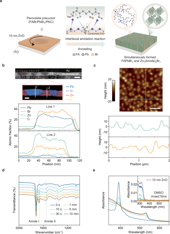
a Schematics of formation of the perovskite layer. b Cross-section STEM image of an ITO/ZnO/perovskite/Au device (scale bar, 100 nm) and the corresponding EDS characterization from the areas marked in STEM image (scale bar, 50 nm), and EDS profiles of Pb, Br, Zn, and C elements derived from the vertical white lines indicated on EDS mapping image. c AFM height images and multiple line scans of the FAPbBr3 films. Scale bar, 500 nm. ATR-FTIR spectra (d) and UV-Vis absorption spectra (e) of the perovskite films at different annealing times, and the absorption spectra of 10 nm ZnO layers and DMSO-rinsed perovskite films (inset in (e)).
We then proceed to monitor the crystallization process of the 3D FAPbBr3 perovskite films by using a range of film characterization techniques. Attenuated total reflection Fourier-transform infrared (ATR-FTIR) spectra (Fig. 1d) of the perovskite films showed that the amide signal become evident and remains almost the same after 1 min of annealing. Notably, the absence of these peaks in the control sample without ZnO underscores that the sacrificial ZnO layer is essential for initiating the interfacial amidation reaction (Supplementary Fig. 3a). Ultraviolet-visible (UV-vis) absorption spectra revealed that the interfacial reaction leads to the formation of 3D FAPbBr3 perovskites and the consumption of the ZnO substrates. The absorption spectra (Fig. 1e) of the perovskite films showed that the strong absorption peaks at higher energies gradually disappear while the perovskite absorption edge at around 532 nm becomes dominant within the annealing time of 1 min, suggesting the transformation of low-dimensional phases into 3D perovskite films16,17,26. We then washed off the perovskite films with a dimethyl sulfoxide (DMSO) solution to expose the underlying ZnO layers. For the perovskite films annealed for 1 min, the corresponding DMSO-rinsed sample showed an insignificant absorption signal (inset in Fig. 1e), indicating that the ZnO layer was completely consumed during the interfacial amidation reaction. The photoluminescence (PL) spectra (Supplementary Fig. 4a) showed that the PL peak exhibited a slight redshift upon increasing the annealing time of the perovskite films. X-ray diffraction (XRD) patterns (Supplementary Fig. 4b) confirmed the existence of low-dimensional perovskite phases at the initial annealing times. In addition, the perovskite films exhibited significant enhancement in crystallinity with the increased annealing time, as evidenced by the rapid increase of the XRD peak intensity. We note that XRD patterns of control samples without ZnO showed no appearance of the perovskite phase (Supplementary Fig. 3b), highlighting the critical role of the interfacial amidation reaction on the formation of 3D FAPbBr3 perovskite. AFM images (Supplementary Fig. 5) further revealed that as the annealing time increased, the perovskite grains grew from smaller sizes into larger and more faceted structures. We notice once again that the Znx(Amide)yBrz complex remains around the perovskite grains during their formation and growth, passivating the grains like other Zn-amine complex27.
To evaluate the emission properties of the FAPbBr3 perovskite films, we first carried out time-dependent PL measurements on the films under continuous annealing at 100 °C. By tracking the PL intensities over time (Fig. 2a), we observed that the samples maintained ~90% of their initial PL intensity after 60 min of annealing, indicating their decent thermal stability at elevated temperatures. Their thermal stability was further confirmed by their almost unchanged absorption properties, crystallinity, and morphological characteristics after annealing at 100 °C for 60 min (Supplementary Fig. 6). PLQY measurements showed that FAPbBr3 films displayed a high PLQY reaching 80% (Fig. 2b). We also observed a trap saturation process characterized by a notable increase in PLQY at extremely low excitation intensities in a range of ∽0.1-1 pJ cm−2 (Fig. 2b), corresponding to ∽1010-1011 cm−3 excited carrier density (Supplementary Note 2 and Supplementary Fig. 7). Importantly, the PLQY of the films can be maintained at a high value of ~70% across a broad excitation range from 1 pJ cm−2 to 0.2 μJ cm−2 (Fig. 2b), suggesting that the trap-assisted nonradiative recombination is strongly diminished in 3D FAPbBr3 films. Power-dependent time-resolved photoluminescence (TR-PL) characterizations further validated their low trap density. The PL decay collected at the lowest carrier density of 2.7 × 1011 cm−3 showed a negligible trapping behavior, indicated by the absence of sharp PL decay at the initial time (Inset in Fig. 2c). Importantly, the PL decay time of these FAPbBr3 films was noticeably longer compared to other reports26,28,29, showing a value of 4.5 μs within the linear PLQY range (Supplementary Note 3 and Supplementary Table 2). TR-PL measurements at different excitation intensities (Fig. 2c) indicated that the Auger recombination starts to dominate at an excited carrier density of 5.5 × 1015 cm−3. By fitting the power-dependent integrated PL data using a generic model30, the trap density of 3D FAPbBr3 films was determined to be 1.2 × 1010 cm−3 (Supplementary Note 4 and Supplementary Fig. 8), which is comparable to the value reported for FAPbBr3 single crystals (9.6 × 109 cm−3)31.
Fig. 2: Luminescence properties of 3D FAPbBr3 films.
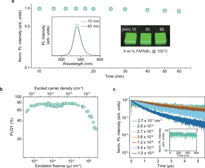
a Thermal PL stability of FAPbBr3 films under continuous annealing at 100 °C. Insets show PL spectra of the perovskite films at two different annealing times and a photograph of the green emitting films under 365 nm UV excitation. b Excitation-intensity-dependent PLQYs of the perovskite film. c Time-resolved PL decay transients of the perovskite film under different excitation intensities. The inset shows the initial PL decay collected at the lowest carrier density of 2.7 × 1011 cm−3.
We further noticed that the key to depositing high-quality FAPbBr3 films on ZnO substrates lies in precisely controlling the thickness of the oxide layer, which ensures efficient interfacial amidation and complete consumption of the sacrificial ZnO layer. To illustrate this fact, we deposited 9 wt.% perovskite precursor solution on top of the 5 nm and 20 nm ZnO layers, respectively. For the samples deposited on 5 nm ZnO substrates, both the absorption spectra and XRD pattern (Supplementary Fig. 9) revealed the existence of a significant portion of low-dimensional perovskite phases. In contrast, the perovskite films deposited on 20 nm ZnO substrates showed pure 3D perovskite features (Supplementary Fig. 10). However, these films had reduced thermal stability, as evidenced by a dramatic decrease in PL intensity under continuous annealing at 100 °C (Supplementary Fig. 11). Additionally, upon removing the perovskite film deposited on 20 nm ZnO through rinsing with DMSO, ~10 nm of unreacted ZnO was revealed (Supplementary Fig. 12). This residual ZnO may cause continuous deprotonation of the FA+ cations and the subsequent decomposition of the perovskite films16.
All-inorganic architecture perovskite light-emitting diodes
The decent PL properties and the significantly improved stability of FAPbBr3 films prompted us to use them in perovskite LEDs. We have proposed a device architecture featuring a perovskite emitting layer sandwiched between a 2-(3,6-dibromo-9H-carbazol-9-yl) ethyl] phosphonic acid (Br-2PACz) SAM and a bilayer oxide EIL comprising 10 nm ZnO-S and 10 nm ALD-ZnO. The Br-2PACz modified ITO substrate, with a work function of 5.5 eV, ensured efficient hole injection (Supplementary Fig. 13). Cross-sectional STEM images of these LEDs display a distinct island-like structure of perovskite (Fig. 3a), which is consistent with observations from the ITO/ZnO/perovskite/Au device (Fig. 1c) and is beneficial for enhancing light out-coupling efficiency4. We note that the sacrificial ZnO layer was completely consumed during the interfacial reaction, and thus it does not serve as a charge-transporting layer in the operational device.
Fig. 3: All-inorganic architecture of perovskite LEDs based on FAPbBr3 films.

a Cross-sectional STEM image of a full all-inorganic architecture device. Scale bar, 100 nm. b J-V curves for the electron-only devices (ITO/Al/oxide EILs/Ag) based on the 50 nm ZnO-S films and bilayer 10 nm ZnO-S/40 nm ALD-ZnO films. c PLQYs for the pristine FAPbBr3 film, the FAPbBr3/ALD-ZnO film, the FAPbBr3/ZnO-S film, and the FAPbBr3/ZnO-S/ALD-ZnO film deposited on quartz substrates. Error bars correspond to the standard deviation. d EL spectra of a perovskite LED under different luminance. Inset shows a photograph of an operating green-emitting device with the City University of Hong Kong (CITYU) logo. e J-V-L curves of the champion device. f EQE, and PCE versus the current density characteristics of the champion device. g Stability data at various initial brightness. The inset shows acceleration factors (n) fitted based on the empirical relationship ?0??50 = constant.
We further designed a bilayer ZnO-S/ALD-ZnO EIL to minimize interfacial quenching while ensuring efficient electron transport. Previous studies found that ZnO-S EILs exhibited minimal quenching of the perovskite emission but suffered from low electrical conductivity due to the long carbon chain ligands on the ZnO-S surface25. To address this issue, we incorporated an ALD-ZnO layer to enhance electron transport. Electrical analyses of electron-only devices with an ITO/Al/oxide EILs (~50 nm)/Ag structure demonstrated a significant (two orders of magnitude) increase in current densities upon introducing the ALD-ZnO layer (Fig. 3b). PLQY measurements of the FAPbBr3 films in contact with different oxide EILs showed that direct deposition of an ALD-ZnO layer on the FAPbBr3 film resulted in severe interfacial emission quenching, leading to rather low PLQY of 39% (Fig. 3c). SEM characterizations revealed that the interfacial quenching originated from the damage to perovskite layers during the ALD process, which was significantly mitigated by introducing a ZnO-S interlayer (Supplementary Fig. 14). As a result, the FAPbBr3 films interfaced with the bilayer ZnO-S/ALD-ZnO EIL maintained a high PLQY of 71% (Fig. 3c), suggesting significantly suppressed interfacial quenching at the FAPbBr3/bilayer ZnO interface.
The perovskite LEDs employing the ZnO-S/ALD-ZnO EIL exhibited remarkable optoelectronic properties. They maintained identical green EL peak at 540 nm with a narrow full width at half maximum (FWHM) of ~21 nm across a wide brightness range from 100 to 300,000 cd m−2 (Fig. 3d), showcasing the high color purity and distinguished spectral stability. The angle-dependent EL intensity followed a Lambertian profile (Supplementary Fig. 15). Figure 3e presents the current density-voltage-luminance (J-V-L) characteristics of these LEDs, featuring a sub-bandgap turn-on voltage of only 1.9 V (Fig. 3e). The current density increased rapidly once the devices were turned on, yielding a maximum luminance of up to ~312,000 cd m−2. Additionally, due to the suppression of interfacial luminance quenching and efficient electron transport, these devices achieved low driving voltages of 2.3 V and 2.7 V for brightness levels of 10,000 and 100,000 cd m−2, respectively (Fig. 3e), both of which are superior to state-of-the-art green perovskite LEDs (Supplementary Table 3).
As a result of low operation voltages, these perovskite LEDs exhibited a peak PCE of 18.2% and maintained a high PCE of 15.6% at a high current density of 300 mA cm−2 (Fig. 3f), suggesting low-efficiency droop. It is noteworthy that this performance is significantly better than in previous reports, where the highest PCEs achieved for green-emitting perovskite, organic, and quantum dot LEDs without out-coupling enhancement at 300 mA cm−2 were only 13.5%6, 2.7%32, and 5.5%23, respectively. Additionally, our devices achieved a peak EQE of 20.7% (Fig. 3f), and the analysis of 50 devices fabricated using the same procedures revealed an average EQE of 17.9% with a standard deviation of 2.6% (Supplementary Fig. 16), confirming decent reproducibility.
Importantly, these perovskite LEDs not only exhibited high PCEs but also demonstrated significantly extended operational lifetimes. The T50 lifetime is plotted in Fig. 3g for devices operated at different initial brightness levels (L0). Notably, the T50 lifetime was 350 h at an initial brightness of 1000 cd m−2 (Fig. 3g). By fitting the T50 data with an empirical equation ((L0)n × T50 = constant) across a broad range of L0 from ~1000 to ~20,000 cd m−2, we determined an acceleration factor (n) of 1.69. Thus, the projected T50 operational lifetime for the perovskite LEDs was estimated to be 17,000 h at 100 cd m−2.
For comparative analysis, a control perovskite LED without the sacrificial ZnO layer was fabricated, which failed to work due to the unsuccessful formation of the perovskite active layer (Supplementary Fig. 17). Additionally, control devices employing either ZnO-S or the ALD-ZnO films as EILs were also fabricated. Perovskite LEDs with ALD-ZnO EILs failed to operate due to the destruction of the perovskite layer during the ALD process, while devices incorporating ZnO-S EILs exhibited current densities significantly lower (by one order of magnitude) than those with bilayer ZnO EILs (Supplementary Fig. 18a). The decreased current densities resulted in a significant EQE roll-off (a PCE of ~5% at 80 mA cm−2) and a markedly reduced T50 lifetime of 25 h at 1000 cd m−2 (Supplementary Fig. 18c,d). These results underscore the importance of the interfacial reaction and the necessity of using bilayer ZnO EILs to achieve high-performance perovskite LEDs.
Potential of fabricating perovskite films for lasing
To achieve high-quality and thicker FAPbBr3 films for lasing applications, it is crucial to manage the concentration of perovskite precursors and the thickness of the ZnO substrate. As mentioned above, using a 20 nm ZnO substrate with a 9 wt.% precursor resulted in ~10 nm of unreacted ZnO. To address this issue, we increased the precursor concentration to 18 wt.%. Figure 4a displays the absorption spectra of the 18 wt.% perovskite films before and after rinsing with DMSO. The absorption spectra of the pristine perovskite films confirm the formation of 3D FAPbBr3 (Fig. 4a), which is further verified by their XRD patterns (Supplementary Fig. 19). After DMSO rinsing, the absorption spectra showed negligible absorption from the ZnO layer (inset in Fig. 4a), suggesting the complete consumption of the sacrificial ZnO substrate. Similar to the thinner perovskite films demonstrated above, the 18 wt.% perovskite films also exhibited decent stability, retaining over 90% of their initial PL intensity after continuous annealing at 100 °C for 60 min (Fig. 4b). Notably, these perovskite films also showed a high PLQY of 77% and a low trap density of 1.7 × 1010 cm−3 (Supplementary Fig. 20). Benefiting from the remarkable optical properties, the devices based on 18 wt.% perovskite films achieved a peak EQE of 19.4% (Supplementary Fig. 21).
Fig. 4: Characterization of the 18 wt.% FAPbBr3 film deposited on the 20 nm ZnO substrate.

a UV-vis absorption spectrum of the 18 wt.% FAPbBr3 film. The inset shows the spectrum of the corresponding DMSO rinsed FAPbBr3 film. b PL spectra of perovskite films under continuous annealing at 100 °C at two different times. c Evolution of the PL spectra of the 18 wt.% FAPbBr3 film under increasing pump fluence of the femtosecond laser excitation (with a central wavelength of 400 nm and 1 kHz repetition rate). d PL intensities versus the pump fluence, and the determined ASE threshold.
Encouraged by the achieved low trap density of the FAPbBr3 films, we proceeded to study their potential lasing properties. Figure 4c shows the PL spectra of the 18 wt.% perovskite films at various pump fluences. At an excitation fluence of 4.2 μJ cm−2, the emission spectrum shows a conventional PL profile with a peak at 544 nm and a FWHM of ~24 nm (Fig. 4c). Upon increasing the pump fluence, a sharp and intense narrow PL peak emerges at ~555 nm and becomes more prominent, while its FWHM decreases sharply to 8 nm, indicative of amplified spontaneous emission (ASE). The ASE threshold for the 18 wt.% perovskite films was determined to be 13 μJ cm−2 (Fig. 4d), which is comparable to the state-of-the-art ASE thresholds for cavity-free perovskites emitting in the green part of the spectrum (Supplementary Table 4).
In summary, we introduced a method to significantly enhance the performance of green perovskite LEDs through the optimization of interfacial chemistry and device architecture. By employing a straightforward interfacial amidation reaction on sacrificial ZnO layers, we successfully fabricated high-quality FAPbBr3 perovskite films with a controllable thickness. These films exhibited a low trap density (~1010 cm−3), comparable to that of single FAPbBr3 perovskite crystals. We integrated these FAPbBr3 films into a perovskite LED with a mono-molecular HIL and an all-inorganic bilayer EIL configuration. The resultant devices not only achieved champion values for brightness (312,000 cd m−2) and PCEs (15.6% at 300 mA cm−2) but also set benchmarks for perovskite LEDs in terms of extended operational stability (T50 lifetime of 17,000 h at 100 cd m−2). Moreover, the optimized perovskite films demonstrated a low ASE threshold of 13 μJ cm−2, which opens up avenues for the development of perovskite-based electrically pumped lasers, further broadening the practical applications of perovskites in optoelectronic devices.
Methods
Materials
Zinc acetate dihydrate (98%), tetramethylammonium hydroxide (TMAH, 98%), lithium hydroxide (LiOH, 98%), lead bromide (PbBr2, 99.999%), and 2-ethylhexane-1-thiol (97%) were purchased from Sigma-Aldrich. Formamidine hydrobromide (FABr, 99%), 2-(3,6-dibromo-9H-carbazol-9-yl)ethyl]phosphonic acid (Br-2PACz, 99%), and pimelic acid (PAC, 98%) were purchased from TCI. Dimethyl sulfoxide (DMSO, HPLC grade), ethanol (extra dry, 99.5%), chlorobenzene (CB, anhydrous, 99.8%), isopropanol (IPA, HPLC, 99.5%) and ethyl acetate (HPLC grade) were purchased from Acros. N-octane (anhydrous, 99%) was purchased from Thermos Scientific. All the chemicals were used as received.
Synthesis of ZnO nanoparticles
ZnO nanoparticles were synthesized through a solution precipitation method previously described in our work33. Briefly, a 2 mmol LiOH solution in 20 mL of ethanol was rapidly injected into a 1 mmol Zn(CH3COO)2 solution in DMSO (20 mL). The mixture was subsequently reacted at 50°C for 1 h under ambient conditions. The nanoparticles were purified by undergoing two rounds of dispersion and precipitation using a mix of ethanol and ethyl acetate solution. ZnO nanoparticles were re-dissolved in ethanol and filtered using a 0.22 µm PTFE filter before use. We note that the ratio of Zn(CH3COO)2 to LiOH was adjusted to 1:1 to prepare the ZnO nanoparticles with larger sizes for thiol-ligand exchange.
Thiol-ligand exchange on ZnO nanoparticles
By adding a solution of TMAH in ethanol into 2-ethylhexane-1-thiol, the pH of the thiol-ligand solution was tuned to 8-9. Subsequently, the ZnO nanoparticles solution was mixed with the thiol-ligand solution and stirred for 2 min. The mixture was precipitated by dispersing/precipitating three times using the combination of n-octane/ethanol. The resulting ZnO-S nanoparticles were redispersed in n-octane and filtered using a 0.22 µm PTFE filter before use.
Atomic layer deposition of ZnO layers
Compact ZnO layers were prepared using an ALD System (GEMStar XTTM). The precursors used for the deposition of ALD-ZnO were ZnEt2 and H2O, and the deposition was conducted at room temperature. High-purity Ar was used as the carrier and purging gas with a process pressure of 0.4 Torr. The ALD program was operated as follows: 30 ms pulse of ZnEt2, 20 s purge, and then 20 ms pulse of H2O, 15 s purge for every full cycle. The ALD-ZnO layers were deposited using 150 cycles (~10 nm thickness), a process that typically takes 1 to 1.5 h.
Preparation of perovskite precursor solution
The perovskite precursor solution was prepared by dissolving FABr:PbBr2:PAC at a molar ratio of 2.8:1:0.6 in DMSO. The precursor solution was stirred at 30°C overnight in a nitrogen-filled glovebox (O2 < 1 p.p.m., H2O < 1 p.p.m.) before spin coating.
Device fabrication
Br-2PACz in IPA solution (0.5 mg mL−1) was spin-coated onto the ITO-coated glass substrates at 2000 r.p.m. for 30 s, and baked at 120°C for 15 min in a nitrogen-filled glovebox (O2 < 1 p.p.m., H2O < 1 p.p.m.). ZnO nanoparticles in ethanol solutions (4 mg mL−1) were deposited onto the Br-2PACz layer by spin coating at 2000 r.p.m. for 30 s. ZnO layers were baked at 120°C for 10 min before the deposition of the perovskites. Perovskite precursor solutions were spin-coated onto the ZnO layers at 4000 r.p.m. for 120 s and annealed at 100 °C for 10 min. During the deposition of perovskite films, 100 μl of CB solution was applied to the film approximately 20 s after the start of spinning. The ZnO-S nanoparticles in n-octane solutions (8 mg mL−1) were spin-coated at 2000 r.p.m. for 45 s, followed by baking at 70°C for 2 min. Then, the ALD-ZnO layer was deposited using the ALD system. Finally, silver electrodes (100 nm) were deposited using a thermal evaporation system (Angstrom) with a pressure of ∼3 × 10⁻⁷ Torr. The device’s active area was determined to be 4.3 mm2.
Characterization
Absorption spectra were collected using a Shimadzu 3600i Plus UV-IR spectrometer. FTIR spectra were obtained on a PerkinElmer spectrometer. XRD patterns were recorded using a D2 PHASER XE-T X-ray Diffractometer System. UPS analysis was performed on an X-ray photoelectron spectrometer (ESCALAB 250Xi, Thermo Scientific) in a high vacuum chamber that maintains a vacuum below 2 × 10⁻¹⁰ Pa. A double-differentially pumped He discharge lamp (hν = 21.22 eV) with a − 5 V bias and a pass energy of 2 eV was used. The thickness of thin films was determined using a Bruker Dektak XT profilometer. A dual-beam focused-ion-beam system (Helios G5 UX) was utilized for preparing cross-sectional samples, which were subsequently imaged on a transmission electron microscope (Thermo Fisher Talos F200E) equipped with an energy-dispersive X-ray spectroscopy system. AFM measurements were performed on a Dimension Icon AFM (Bruker) using the tapping mode under ambient conditions. Time-resolved photoluminescence (TRPL) decays were measured by exciting the sample with a 400 nm, 100 fs laser generated through frequency doubling the output of a mode-locked titanium sapphire oscillator laser tuned to 800 nm. A variable ND wheel attenuated the beam, and the power before the sample was measured with a laser power meter (Newport). The laser was focused on the sample, and the PL signal was collected into a monochromator (Acton Spectrapro 275) using a pair of achromatic lenses. The peak wavelength of the PL was dispersed by 1200 lines mm−1 grating onto a photon counter and time-correlated single photon counting was carried out using a Becker and Hickl system. For time-integrated PL measurements, the signal was diverted into a fibre-coupled spectrometer (Acton Spectrapro 500i) equipped with a Peltier-cooled EMCCD (Andor Newton). A commercial system (XPQY-EQE-350-1100) with a Keithley 2400 source meter, an integrated sphere (GPS-4P-SL, Labsphere) and a photodetector array (S7031-1006, Hamamatsu Photonics) was used to record the PLQYs and PL spectrum of the perovskite films, and the J-L-V curves, EL spectra, and EQE of the perovskite LEDs. T50 operational lifetimes of the LEDs were collected using an ageing system with an embedded photodiode (Guangzhou New Vision Opto-Electronic Technology Co., Ltd.). A highly sensitive CCD spectrometer (Hamamatsu C7473-46) measured the angle-dependent EL intensity, coupled with a Keithley 2400 source meter and a precision rotating stage.
Data availability
The datasets generated during and/or analysed during the current study are available from the corresponding author on request.