Interfacial Trap Effect Modulation of Organic Phototransistors for Artificial Vision System
Jul. 21 , 2024photonics1
Abstract
Artificial photoelectric synaptic devices are promising candidates for simulating the perception, processing, and memory functions of biological visual information. Dielectric layer interface modification is a simple and effective strategy for the fabrication of light stimulated synaptic devices. In this work, the dielectric layer interface was tuned by varying the terminating groups of self-assembled monolayers (SAMs), whereas the polymer polydiketopyrrolopyrrole-selenophene with hybridized siloxane side chains (PTDPPSe-4Si) was used as the active layer for fabrication of the transistor devices. Enhanced optoelectronic performance was observed in the fabricated devices that were treated by pentafluorophenylpropyltrichlorosilane (FPPTS) due to the presence of more interfacial charge traps. The photosensitivity and detection rate were found to be up to 105 and 1011 Jones, respectively. Furthermore, it was also shown experimentally that the interfacial charge trapping effect was caused by a combined effect of electron trapping by the SAMs-modified interface and traps present within the active layer. Biological synaptic plasticity was successfully simulated using FPPTS/PTDPPSe-4Si-based devices. The memory and forgetting processes of biomimetic visual information were also simulated. Finally, conventional neural networks were used for image recognition, achieving a recognition rate of over 95%.
This publication is licensed under the terms of your institutional subscription. Request reuse permissions.
Visual perception is a critical function of the eye that senses light stimuli and contributes to the acquisition of external information in the daily lives of humans in a significant way. (1) At least 80% of the information about our surroundings are obtained through vision. (2) Inspired by biological vision, the construction of artificial visual neural networks will be of great importance. (3,4) The biomimetic optoelectronic synaptic devices are the basis for developing artificial visual neural networks owing to their ability to integrate the functions of detection, processing and retaining memory of the external light stimulus. (5−7)
Various types of optoelectronic synaptic devices have been reported. Most of them have primarily been focused on tri/multiterminal transistors and two-terminal resistance switching memories. (8−13) Among these, transistor based devices have the advantage of higher integration and can also employ gates to modulate synaptic behavior to achieve signal amplification in bionic vision. (12) Transistor devices facilitating/suppressing the separation/binding of photogenerated electron–hole pairs are one of the necessary conditions for realizing biomimetic synapses. (14−16) To achieve high photoelectric conversion and long-lasting photoconductivity, various methods have been explored. Tuning the device structure design, modulation of the molecular structure of the active layer, and variation of the dielectric layer interface are some commonly applied techniques. (11,17) Among all these approaches, modification of the dielectric layer interface is a simple and effective strategy for improving photoconversion performance. (18,19) A reversible charge trapping phenomenon was simulated by Zhong et al. through the introduction of a poly(2-vinylnaphthalene) electret layer, which exhibited various synaptic behaviors at primary, young and mature stages. (18) Polyacrylonitrile (PAN) films were used as the dielectric layer for fabrication of organic field effect transistors (OFET) in another study carried out by Dai et al. Enhancement of the charge trapping effect that enabled the devices to exhibit excellent synapse-like behavior was attributed to the presence of polar groups in the PAN films. (20) Zhu et al. prepared p-fluorinated polystyrene (p-FPS) for dielectric layers in OFET devices by side-chain engineering. (19) The introduction of p-FPS was shown to increase the trap density, resulting in efficient photonic memory and excellent artificial synaptic properties. These studies suggest that the carrier transport interface charge trapping effect of the OFET is a promising option. Self-assembled monolayers (SAMs) treatment of dielectric layers in OFET have been actively studied in the early history of organic electronics, but the systematic study of its effect on the synaptic devices has been rare. (21,22)
In this work, SAMs with different terminal groups were prepared and used at the dielectric layer interface. The PTDPPSe-4Si polymer exhibiting good electrical properties was chosen as the active layer for the preparation of the OFET devices. The morphology and microstructure of the semiconductor films were observed using atomic force microscopy (AFM) and high-resolution field emission scanning electron microscope (FESEM). The optoelectronic properties of the SAMs/PTDPPSe-4Si devices were then systematically investigated. Thereafter, FPPTS/PTDPPSe-4Si based devices were simulated for various bionic synaptic behaviors. The learning, forgetting, and recognition functions of biomimetic vision were also simulated.
Results and Discussion
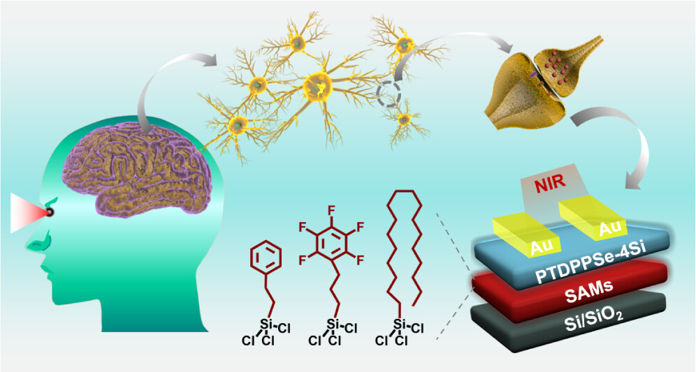
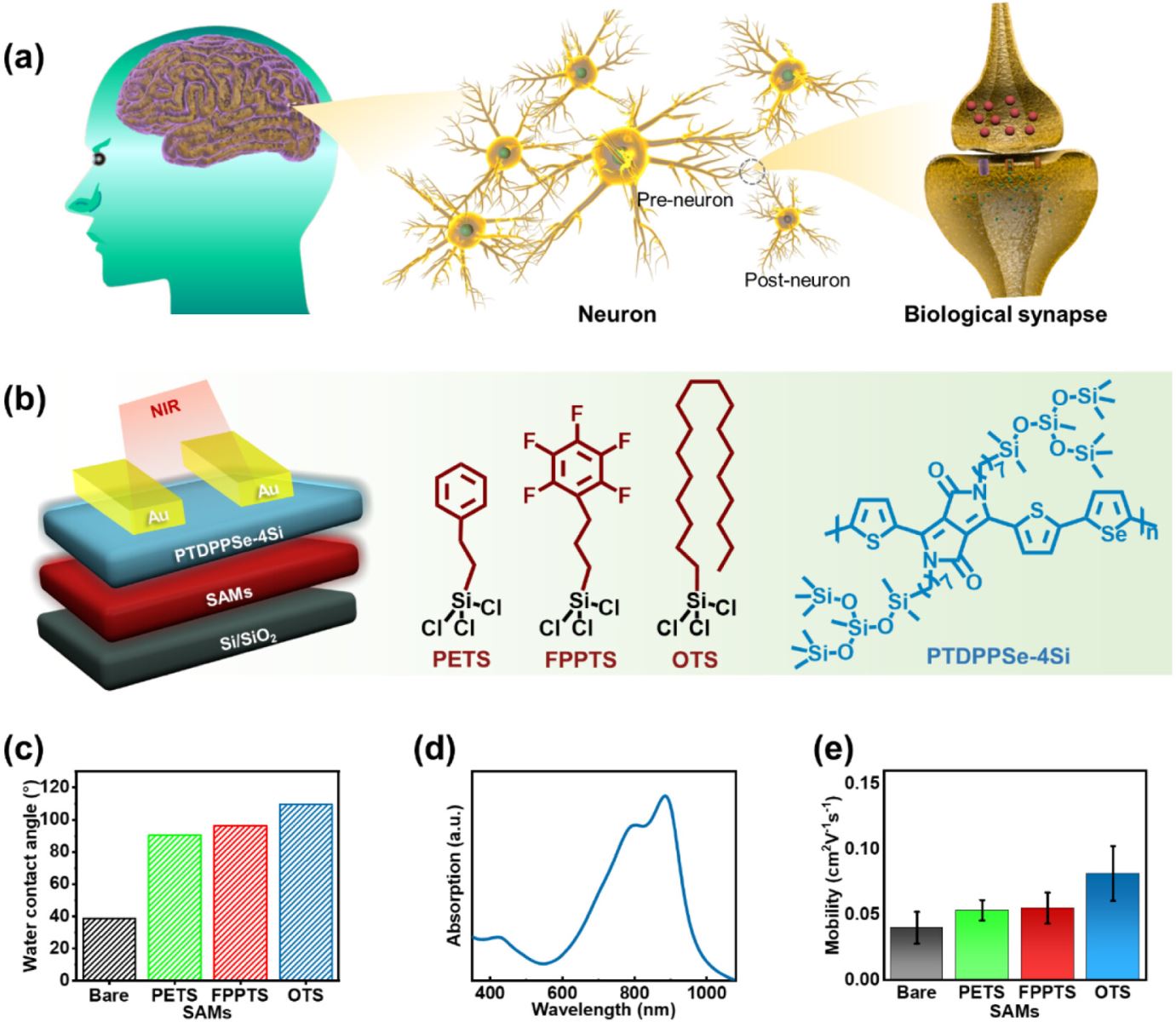
The human brain is made up of billions of neurons for memory and signal processing, and at the end of each neuron is an axon, which is made up of many branches. The place where two neurons come into contact and pass information is called a synapse (Figure 1a). (23,24) In this work, biomimetic synaptic devices based on SAMs/organic semiconductors were fabricated using a simple bottom-gate-top-contact transistor structure. As shown in Figure 1b, phenethyltrichlorosilane (PETS), pentafluorophenylpropyltrichlorosilane (FPPTS), and octadecyltrichlorosilane (OTS) were used as modified layers for the Si/SiO2 substrates. Details of the preparation process are provided in the experimental section. Characterization revealed that water contact angles of the Si/SiO2 substrates treated by SAMs were larger in comparison to the untreated ones, as can be seen in Figures 1c and S1a–d. This was due to the introduction of hydrophobic chain segments on the substrates, confirming successful preparation of the SAMs. (21) The PTDPPSe-4Si polymer, which has been reported in previous studies was chosen as the device active layer keeping in view its excellent electrical properties, as well as easy processability. (25) In addition, PTDPPSe-4Si exhibited high light absorption in the 800–900 nm spectral region (Figure 1d), with an optical bandgap of approximately 1.24 eV, allowing stimulated response in the near-infrared (NIR) spectral region. PETS/PTDPPSe-4Si, FPPTS/PTDPPSe-4Si and OTS/PTDPPSe-4Si-based devices were prepared by spin-coating PTDPPSe-4Si solution onto Si/SiO2 substrates with different SAMs. Additionally, Bare/PTDPPSe-4Si devices without any treatment by SAMs were taken as the control samples. The obtained transfer and output curves for each device are provided in Figures S2a–f, respectively. It was found that all of them exhibited significant hysteresis, which indicated the presence of a large number of traps at the carrier transport interface. (26) This is detrimental to carrier transport in the dark state, but beneficial in improving the optoelectronic conversion performance of the device. (27) The SAMs/PTDPPSe-4Si devices exhibited a higher average mobility in comparison to the Bare/PTDPPSe-4Si devices, as shown in Figure 1e. The average mobilities of Bare, PETS, FPTS and OTS-based devices were calculated to be 0.040 cm2V–1s–1, 0.053 cm2V–1s–1, 0.055 cm2V–1s–1 and 0.082 cm2V–1s–1, respectively. Covering SiO2 with a SAM layer with hydrophobic chain segments would shield most of the SiO2 surface traps. This may be the main reason for the improved performance of both of the SAM/PTDPPSe-4Si devices. Among them, the OTS/PTDPPSe-4Si devices have the highest electrical performance, which is mainly due to the fact that the long alkyl chains in OTS exhibit good stacking and the best shielding against traps. (22) It was also found that the on/off current ratio for all devices exceeded the value of 105 and they also exhibited lower threshold voltages (Figure S3 ). This indicated that modification of the dielectric surface by SAMs is an effective method to improve the electrical performance of the devices.
Figure 1
Figure 1. (a) Schematic diagram illustrating the nervous system of the human brain. (b) SAMs/PTDPPSe-4Si transistor device structure (left), molecular structure of PETS, FPPTS, OTS, and PTDPPSe-4Si (right). (c) Comparison of water contact angles for different SAMs/SiO2/Si structures. (d) UV–vis absorption spectra for the PTDPPSe-4Si film. (e) Comparison of the mobility for different SAMs/PTDPPSe-4Si-based devices.
Film morphology of the semiconductors was studied using AFM. As shown in Figure S4a–d, the PTDPPSe-4Si films deposited on different SAMs were dense nanofibers that exhibited reduced surface roughness compared to the Bare/PTDPPSe-4Si films. This may also contribute to improved electrical performance. These results were also consistent with the results obtained from SEM characterization, which are presented in Figure S5a–d.
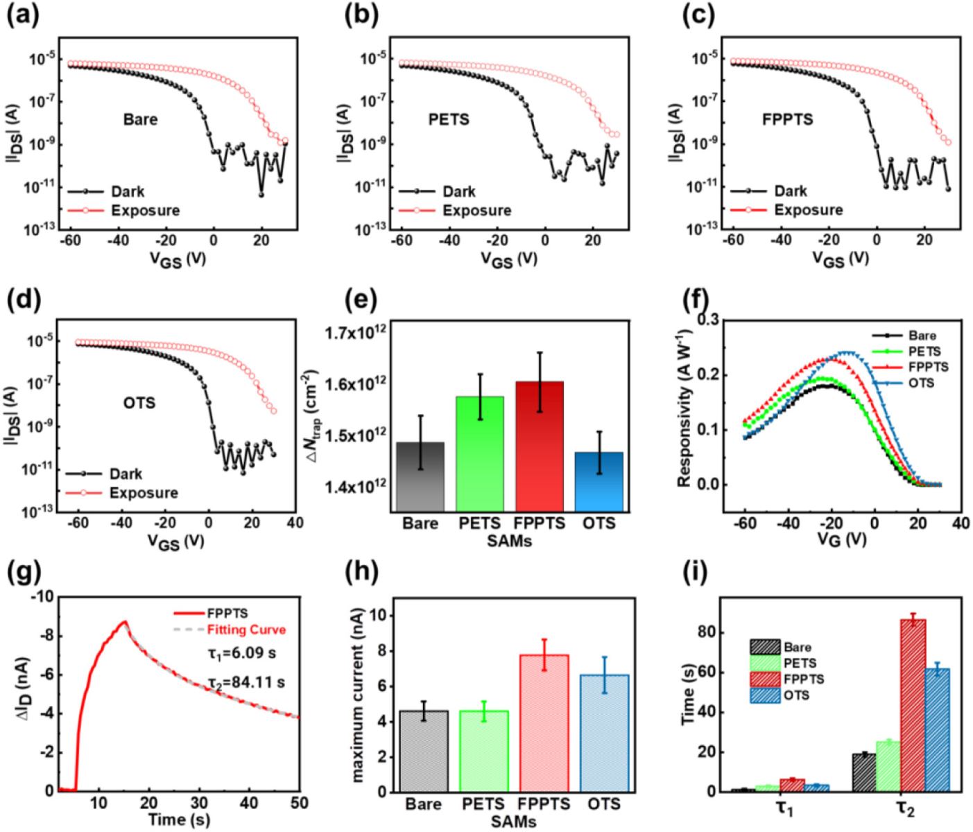
The charge trapping effect at the carrier transport interface has a significant impact on the optoelectronic performance of the device. (23) In this study, the optoelectronic performance of SAMs/PTDPPSe-4Si devices was systematically been investigated. A wavelength of 808 nm in the NIR region of the UV–vis absorption spectrum was used as the external stimulus. First, the transfer characteristic curves for each device in the dark and under light irradiation (17.5 mW cm–2) were obtained, which are provided in Figure 2a-d. It was found that all of the transfer curves exhibited a significant positive shift under NIR illumination, which corresponded to the large hysteresis in the results obtained from the electrical performance characterization. This can be attributed to the presence of a large number of charge traps at the carrier transport interface in each device. (28) The variation in ΔVth was used to estimate the number of captured photogenerated carriers at the dielectric/active layer interface, and ΔVth is the change in threshold voltage extracted from the device transfer curve before and after light stimulation, see Supporting Information for details. (26) The ΔNtrap represents the number of traps with carriers captured at the dielectric-active layer interface. which was calculated using the following mathematical relationship:
Δ??trap=Δ??th·????
(1)
where e represents the fundamental charge and C represents capacitance of the dielectric layer. As shown in Figure 2e and Table S1, the interface of the OTS/PTDPPSe-4Si device exhibited the lowest number of trapped photogenerated carriers in comparison to the other three devices. This indicated that the surface trap passivation of OTS-modified SiO2 was relatively better, which facilitated the charge transport mechanism in the dark state. (22) In contrast, the FPPTS/PTDPPSe-4Si device exhibited the largest ΔNtrap, indicating that the carrier transport interface of this device displayed a higher, more efficient charge capture capability. In order to verify whether the UV ozone treatment on the SAM surface affects the electron trapping of the direct spin-coated devices, control experiments were done. The devices were prepared by direct spin-coating PTDPPSe-4Si on Si/SiO2/OTS substrate without UV ozone treatment. The transfer curves were compared between dark and light conditions (Figure S6a,b). According to eq 1, the number of traps to capture photocarriers is about 1.43 × 10¹², which is similar compared with the number of traps after UV-ozone treatment (1.49 × 10¹²). It indicates that the effect of UV ozone treatment is negligible. The responsivity (R), photosensitivity (P), and detectivity (D*) of the SAMs/PTDPPSe-4Si devices were further evaluated quantitatively. (29,30) The value of R was calculated using the following mathematical expression:
??=??light−??dark??p·??
(2)
where Idark is the current obtained under dark conditions, Ilight is the current value under illumination, and S is the effective area irradiated by light (1 × 10⁻³ cm2). Light intensity ip was 17.5 mW cm–2. The photosensitivity (P) is one of the most important parameters required to calculate the light sensitivity of the device, (30) and it is defined by the following expression:
??=??light−??dark??dark
(3)
Figure 2
Figure 2. (a–d) Transfer characteristic curves for the devices corresponding to direct spin-coated PTDPPSe-4Si thin films on different substrates in the dark and under NIR illumination (VD = −60 V). (e) Comparison of the number of photogenerated carriers trapped at the dielectric-active layer interface. Comparison of (f) responsivity (R) of the SAMs/PTDPPSe-4Si and Bare/PTDPPSe-4Si-based devices under NIR illumination. The ID–Time optical response curves for (g) FPPTS/PTDPPSe-4Si device measured at VD = −5 V and VG = −5 V. The ID decay for the devices with different SAMs were curve fit separately using a double exponential response equation (gray dashed line). (h) Maximum current statistics obtained from the ID–Time optical response curves for different devices. (i) Statistics of fast decay time τ1 and slow decay time τ2 for different devices.
The D* value for the shot-noise-limited case provides a measure of the smallest signal that can be detected by the device and is calculated using
??∗=??2????dark/??‾‾‾‾‾‾‾‾‾√
(4)
After calculation of these parameters using the above equations, it was clear that the devices based on the OTS/PTDPPSe-4Si and FPPTS/PTDPPSe-4Si exhibited high R, P and D* values (Figures 2f, S7a,b, and Table S1). The value of R exceeded 0.2 A W1–, and the value for P was found to be up to 105, whereas the value of D* was calculated to be higher than 1011 Jones. The high detection performance of FPPTS/PTDPPSe-4Si devices can be attributed to the presence of a high number of charge traps at the carrier transport interface. (19) Although the number of carrier traps in the OTS/PTDPPSe-4Si device was low, the higher carrier mobility allowed the photogenerated holes to reach the electrode at a faster rate before recombination, which reduced the complexation of the electron–hole pairs, resulting in better photodetection performance. The more specific reasons are verified and explained later.
The transient optical response of the SAMs/PTDPPSe-4Si and Bare/PTDPPSe-4Si devices was further compared. As shown in Figures 2g and S8a-c, the channel current in each device rose significantly under illumination of the NIR light source with an intensity of 17.5 mW cm–2 for about 8 s. In order to obtain a stable ID-Time test curve output at a lower energy consumption, we chose the test conditions of VG = −5 V and VD = −5 V. ΔID is the value after normalization and represents the current increase under a light pulse. Upon removal of the light source, the photocurrent gradually decayed down. Among the different types of devices, the FPPTS/PTDPPSe-4Si based device exhibited the highest instantaneous photocurrent (Figure 2h), which was due to the fact that FPPTS/PTDPPSe-4Si devices contained a higher number of carrier traps with a good separation between each electron–hole pair, thereby increasing the number of majority carriers present in the channel. To compare photocurrent decay of the different devices, the decay was curve fit using a double exponential equation:
??=??0+??1exp(−??/??1)+??2exp(−??/??2)
(5)
where I0 represents the photocurrent before illumination removal, A1 and A2 are constants, and τ1 and τ2 are the fast and slow decay time constants, respectively. (31) The decay time constant τ1 is usually associated with the fast recombination of photogenerated carriers through shallow traps or between band gaps, while τ2 is associated with the slow release of photogenerated carriers trapped within deep trap states. (27) On the contrary, when fitting the photocurrent increase process using the double exponential function, τ1 and τ2 represent the fast increase and slow increase processes, respectively. As shown in Figure S8a, τ1 and τ2 for photocurrent increase are 0.57 and 3.19 s, respectively, which indicates that the photoresponse current exhibits a rapid increase followed by a slow increase process. Since the photocurrent decay is crucial for the study of the interfacial trap state, the subsequent fitting comparison is done only for the photocurrent decay process. The obtained fitting curves are shown using light gray dashed lines in Figure 2g, Figure S8a-c. The results revealed that the FPPTS/PTDPPSe-4Si device exhibited the highest values for τ1 and τ2 (Figure 2i), which indicated that the electron capture mechanism at the carrier transport interface in this device could moreover be attributed to the deep traps, making it difficult for the captured electrons to recombine. In contrast, the Bare/PTDPPSe-4Si and PETS/PTDPPSe-4Si devices exhibited lower values of τ1 and τ2, indicating that these devices were dominated by the shallow trap capture mechanism, which allowed for the rapid recombination of the captured electrons.
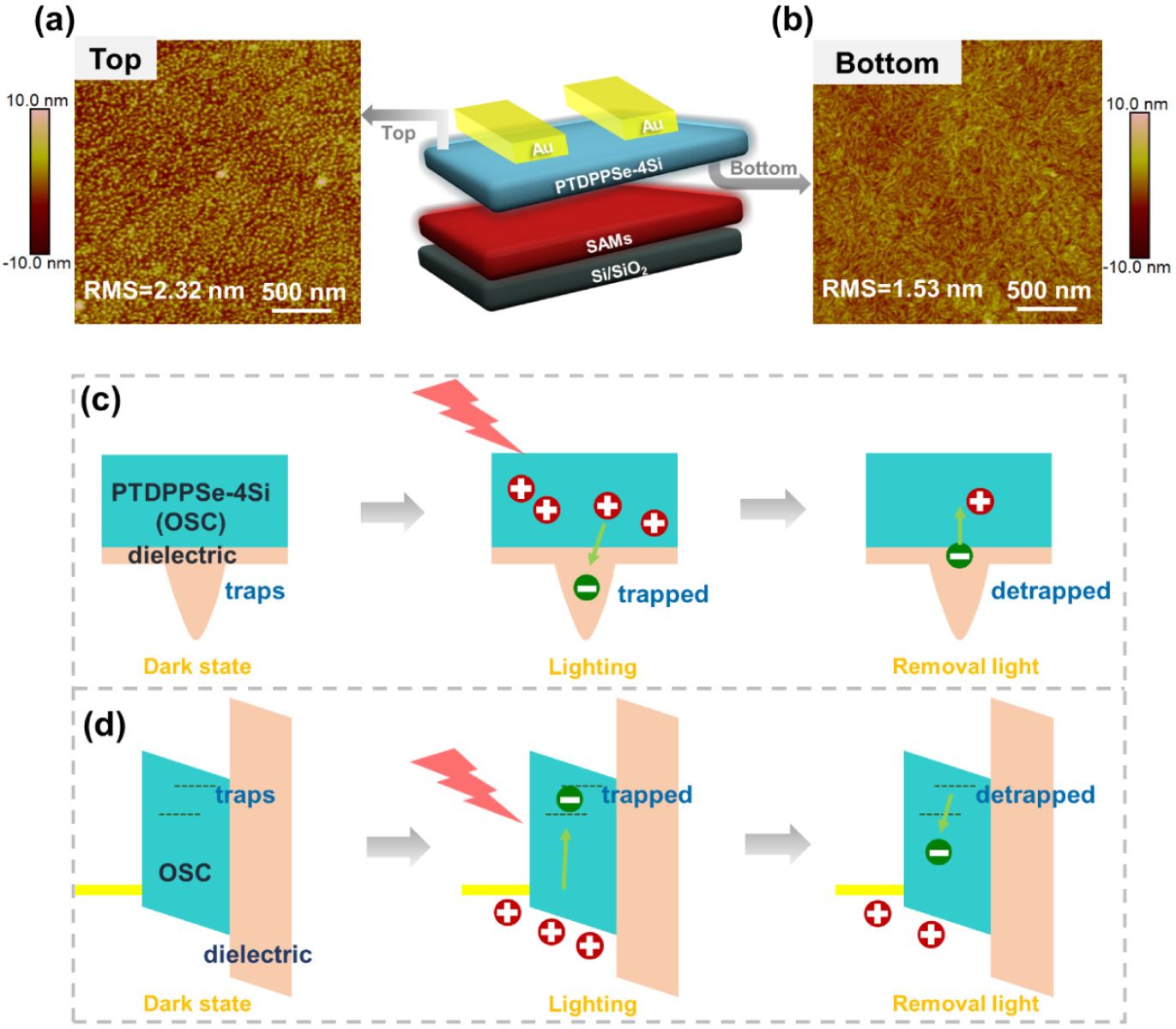
The results of the experimental studies described above showed that the presence of a trap at the carrier transport interface plays an important role in the optoelectronic performance of the device. The traps may have formed due to defects at the dielectric layer interface or in the active layer itself. Control experiments were added and performed to confirm this hypothesis. The predeposited PTDPPSe-4Si films were transferred to different SAMs substrates as well as Bare substrates, and then transistor devices were fabricated (Figure S9). Details of the preparation process are provided in the Experimental Section. The transfer and output characteristic curves for the devices are presented in Figure S10a–h, respectively. It can be seen from the figures that the hysteresis for the devices fabricated in this work was reduced significantly in comparison to the direct spin-coated devices (Figure S2a–d), which indicated that the number of carrier transport traps at the interface was reduced for these devices. (25) The average mobilities of Bare, PETS, FPPTS and OTS-based devices were calculated to be 0.28 cm2V–1s–1, 0.40 cm2V–1s–1, 0.39 cm2V–1s–1 and 0.56 cm2V–1s–1, respectively. The switching ratios for all devices exceeded the value of 104, as shown in Figure S11a,b. A significant improvement in mobility was achieved in comparison with that obtained from direct deposition of layers in semiconductor devices. The top and bottom surface morphology of the transferred film were characterized separately (Figures 3a,b and S12a,b). It was revealed that the top and bottom surfaces have different morphology. The improvement in the electrical properties may be caused by differences in the way the conjugated polymer molecules are stacked on the upper and lower surfaces of the deposited films. Compared to the contact between the semiconductor film and the substrate interface, at the air interface, the semiconductor molecules move with a small bundle, allowing for better molecular stacking when the solvent evaporates, and facilitating carrier transport. (32) As a result, the electrical performance of the device is improved when the upper surface of the transfer-spin-coated deposited film is in contact with the substrate. The difference in the performance of devices corresponding to different semiconductor thin film preparation processes suggests that the carrier trappings partly come from the semiconductor layer.
Figure 3
Figure 3. AFM height maps of (a) the top as well as (b) the bottom of the PTDPPSe-Si4 film after flipping. (c,d) Schematic diagram illustrating the light response mechanism in the device.
To investigate the effect of SAMs on the optoelectronic performance of the devices, the transfer characteristic curves of the transferred thin film devices were obtained in the dark and under light conditions, which are shown in Figure S13a–d. The value of ΔNtrap was calculated using eq 1. From Figure S13e and Table 2, it can be clearly seen that the FPPTS/PTDPPSe-4Si based device exhibited the highest value of ΔNtrap, which is primarily attributed to the strong electron-absorbing property of the -F group in FPPTS. The values of R, P, and D* were calculated using eqs 2–4, respectively. The plots for the variation in these parameters with change in the gate voltage VG are shown in Figure S13f-h and Table 2. The highest values for the R, P, and D* parameters were obtained for the FPPTS/PTDPPSe-4Si based device. This is due to the fact that the FPPTS-modified interface contained a higher number of trapped carriers compared to the other three interfaces. (19) This proved that different modified layers at the dielectric layer interface also have a significant impact on the interfacial carrier trapping effect.
To further verify the above results, the ID–Time response curves were also obtained, as shown in Figure S14a-d. It was revealed that the transient light response currents of the devices based on transferred films all enhanced substantially in comparison to the thin film devices fabricated by using direct spin-coating deposition (Figures S14e and 2h), which is a direct result of the improved electrical performance of the devices. Fitting the decay curve using a double exponential function revealed that the maximum value of τ2 never exceeded 31 s, which is less than half of what was obtained from the directly spin-coated film, as can clearly be seen from a comparison of Figures S14f and 2i. This further confirmed that the presence of defects within the semiconductor was responsible for the interfacial charge trapping mechanism. Despite the high response of the transfer-deposited FPPTS/PTDPPSe-4Si devices, the short decay time of the current is not favorable for the simulation of biomimetic visual long-term memory.
The above control experiments shed more light on the optical response mechanism, clarifying it further, as shown by the results provided in Figure 3c,d. Owing to the narrow bandgap of the PTDPPSe-4Si polymer, the electron–hole generation process took place inside the semiconductor under NIR light irradiation and separation by internal electric field. (33,34) Since traps were present inside both SAMs and semiconductors, the separated electrons were partially confined within trap states of the SAM layer (Figure 3c) and partially trapped by internal traps present within the semiconductor (Figure 3d). This eventually led to an increase in the number of holes and generated a current in response to light illumination. As the light source was removed, the trapped electrons were gradually released and recombined with the holes, resulting in a slow decay of the photocurrent.
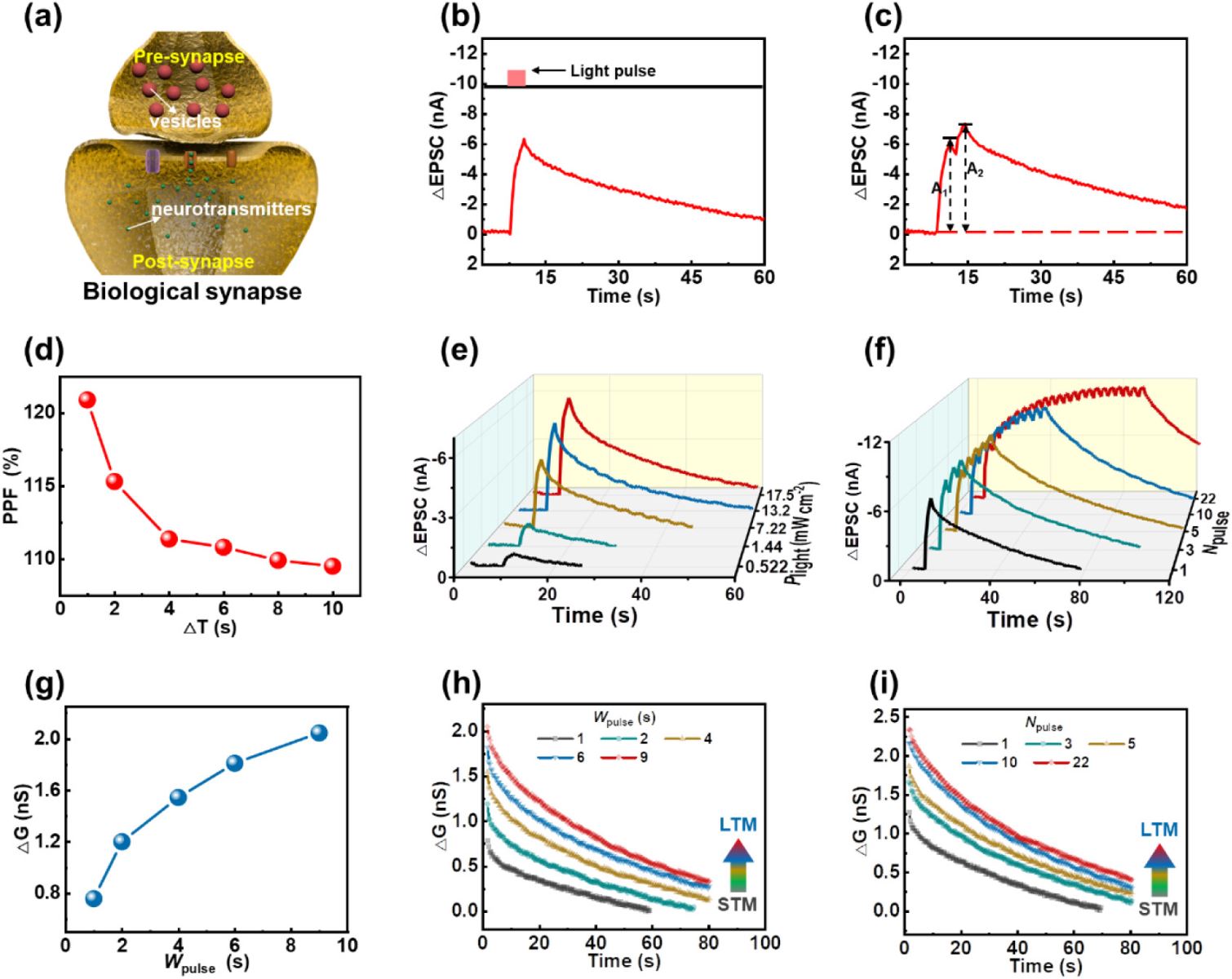
In biological synapses, when a presynaptic neuron receives an external stimulus, a signal is transmitted to the synaptic vesicle, followed by the release of neurotransmitters to the postsynaptic membrane, where the transmitter binds to receptors located in the posterior membrane, triggering a change in potential to transmit the message, as shown in Figure 4a. (35) The transistor devices prepared in this work simulate a similar kind of biological synaptic behavior. The interfacial traps of the device can be used to simulate the receptors in the biological postsynaptic membrane, the NIR light may be considered as the external stimulus, whereas the positive photocurrent signal can be taken as the excitatory postsynaptic current (EPSC). (5) The FPPTS/PTDPPSe-4Si device exhibits the highest charge-trap density and slow photocurrent decay process, which allows for long-term retention of information, an important property required to enable the simulation of bionic memory functions. Therefore, the device was chosen to simulate various bionic synaptic behaviors. As shown in Figure 4b, the EPSC of the device increased when stimulated by an NIR light source with an intensity of 17.5 mW cm–2 for 2 s. The current slowly decayed as the light source was removed, similar to the case for biological synaptic signals. Synaptic plasticity is a property of tunable connections between nerve cells, which is categorized into two main categories, namely short-term plasticity (STP) and long-term plasticity (LTP). (36) Paired pulse facilitation (PPF) is one of the most important properties of STP. (37) It can clearly be seen in Figure 4c that as two light pulses were applied consecutively one after the other, the change in EPSC after the second light pulse was greater than the change in EPSC after the first light pulse. This can be explained by the fact that increase in the EPSC brought upon by the first light pulse had not yet fully decayed to the initial state at the time when the second light pulse was applied. (38) The PPF ratio was further calculated and assessed by varying the time between the two pulses (ΔT). Here, the PPF ratio is defined by the following mathematical expression:
PPF ratio=??2??1×100%
(6)
where A1 and A2 are the EPSC values added for the first and second optical pulses, respectively. (39) As ΔT was gradually increased, the PPF exhibited a decrease in its value, as shown in Figure 4d. This implied that the device had STP characteristics.
Figure 4
Figure 4. (a) Schematic diagram of a biological synapse. (b) Variation of ΔEPSC with time for a single light pulse. (c) Variation of PPF for two consecutive light pulses (Tlight = 2 s, ΔT = 1 s). (d) PPF index as a function of ΔT. (e) Modulation of synaptic plasticity at different light intensities. (f) Modulation of synaptic plasticity at different numbers of light pulses (17.5 mW cm–2, T = 2 s, ΔT = 1 s). (g) Variation of weights at different light pulse times. Comparison of synaptic weight changes with time for different (h) light pulse widths and (i) number of pulses.
Synaptic plasticity plays an vital role in reception of information and learning by living organisms. (3) In this work, the prepared devices also exhibited plasticity in relation to light intensity, light pulse duration, and the number of light pulses. As the light intensity was increased from 0.522 mW cm–2 to 17.5 mW cm–2, the EPSC level also increased from 0.66 nA to 5.89 nA, as shown in Figure 4e. Similar phenomena occurred as the light pulse time and the number of light pulses were raised, as shown in Figures S15 and 4f, respectively. This phenomenon may be attributed to enhancement of the light intensity, light pulse duration, and the number of light pulses, all of which increased the number of captured electrons in the carrier transport interfacial layer, thus leading to an increase in the EPSC. (20) The synaptic plasticity enhancement or facilitation effect was also a manifestation of the increased synaptic weight (ΔG). (40) Here, the channel conductance of the device was used to simulate the parameter of ΔG, which can be defined as the ratio of EPSC to the drain voltage. (41) It was found that ΔG increased with an increase in the light intensity (Figure S16a), light pulse duration (Figure 4g), and the number of light pulses (Figure S16b).
The memory of an organism can be categorized into short-term memory (STM) and long-term memory (LTM) based on duration of the memory. (42) The change in ΔG can be used to imitate the memory level of an organism. As shown in Figure 4h, the memory level increased gradually with an increase in the light stimulation time, thus successfully simulating the transition from STM to LTM. A similar memory effect was observed with the intensity of the light pulses (Figure S17) and the number of light pulses were increased, as shown in Figure 4i. Hence, biological synaptic plasticity as well as memory behavior were successfully simulated.
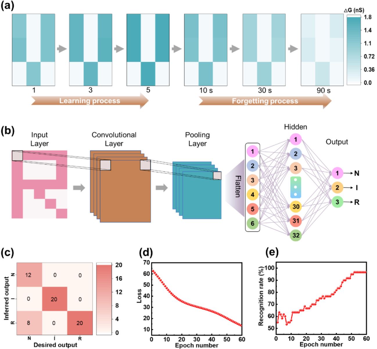
Recognition and memory of images is an important manifestation of visual learning. (42) In this study, the learning and forgetting process of bionic vision was demonstrated using the image. As shown in Figure 5a, increasing the number of learning times from 1 to 5 led to a significant darkening of the image color, which simulated the learning process of bionic vision. At the end of the study, the memory of the images gradually diminished with time. This was quite similar to the learning as well as the forgetting behavior associated with biological vision.
Figure 5
Figure 5. (a) Imaging sequence illustrating biomimetic vision learning and forgetting processes. (b) Schematic diagram of the CNN process for image recognition. (c) Confusion matrix for the optical stimulation neural network. All correct classifications are located on the diagonal of the table. Variation of (d) loss values and (e) recognition rate with the number of training sessions during training of the optically stimulated neural network.
To simulate the recognition of letter images by bionic vision, we constructed a 5 × 7 array of synapses and used a computer system to build a convolutional neural network (CNN), as shown in Figure 5b. The CNN algorithm was implemented using the Python language. See the Support Information for Python language source code. It consisted of a convolutional layer and a fully connected layer. (43) The fully connected layer included input, hidden, and output neuron layers. In the convolution process of feature extraction, four feature maps were obtained from the input pattern image with a size of 5 × 7. Thereafter, 32 feature signals from the flattening layer were passed on to the fully connected network for classification. The phototransistor synaptic device is the basis for the implementation of simulation in CNN simulation. In a 5 × 7 device array, each synaptic device acts as a pixel point. By varying the intensity of the light pulse, nonvolatile current values of different intensities are obtained in the synaptic arrays (Figure S18a,b), and the extracted arrays of current values are simulated by CNN simulation to obtain the recognition accuracy of the final letters. For the recognition test, three patterned images including “N″, “I″ and “R″ were prepared. A data set of 100 different patterns was used for each image, with a training-to-test ratio of 8:2, as shown in Figure S19. The training process is a step-by-step learning process of the neural network, which can be tracked by the color of the diagonal lines in the confusion matrix. As shown in Figure 5c, the maximum inferred output value of each row matched the expected output value of each column, indicating that the alphabetic maps of “N″, “I″ and “R″ were successfully recognized. In addition to that, as the number of training sessions was raised, the loss value was seen to decrease (Figure 5d) and the recognition rate gradually increased to a saturation point, as can be seen in Figure 5e. A high recognition rate of more than 95% was achieved in less than 60 training sessions. This high CNN simulation recognition performance is closely related to the current values extracted from the phototransistors, in addition to the logic structure in the CNN. (43) Thus, it was successfully demonstrated that the constructed artificial synaptic system exhibited a highly accurate letter image recognition capability.
Nevertheless, the prepared optoelectronic synaptic devices still have some challenges in realizing a practical bionic vision system, which is a subsequent issue to focus on. First, the sensitivity of organic semiconductor materials to oxygen and water, which will exhibit degradation in performance over time, can be encapsulated to improve the usability of organic synaptic devices. Second, the size of the prepared organic optoelectronic synaptic devices is much larger than that of biological synapses, and there are challenges in further realizing large-area array preparation, which lacks the small size and high-density characteristics of biological synapses. The full integration of materials, chemistry, physics, and computer science will effectively lower the barriers to the further development of artificial vision systems.
Conclusions
In summary, transistor devices were prepared using SAMs with different terminal groups as the dielectric modification layer and narrow bandgap PTDPPSe-4Si conjugated polymer as the active layer. The optoelectronic properties of the SAMs/PTDPPSe-4Si devices were then systematically investigated. FPPTS/PTDPPSe-4Si based devices with a -F group as the surface terminal group exhibited excellent charge trapping capability. The calculated photosensitivity was found to be up to 105 and the detection rate was obtained to be over 1011 Jones. In addition, it has a long photocurrent decay time. The charge trapping effect was studied by using controlled experiments through a combination of the SAMs and active layers. This interfacial charge trapping effect has various potential applications in the field of biomimetic optoelectronic synapses. The FPPTS/PTDPPSe-4Si device was used to successfully simulate various bionic synaptic functions such as EPSC, PPF, STP and LTP. Also, the image memory and forgetting processes of biological vision were successfully simulated. Finally, the recognition of letter images was successfully achieved by building a CNN with a recognition rate of over 95%. Hence, this work provides a simple and effective strategy for the preparation of bionic light-stimulated synaptic transistors for artificial visual systems.
Experimental Section
Materials
The precursors PETS, FPPTS, and OTS and poly(vinyl alcohol) (PVA, Mw ≈ 9–10 kDa) were commercially purchased, whereas FPPTS and OTS were purchased from Shanghai Aladdin Biochemical Technology Co. PETS and PVA were purchased from Sigma-Aldrich. Lastly, the PTDPPSe-4Si polymer (Mn = 221.3 kDa, PDI = 2.56) was prepared in the lab as for a previously reported study.
Device Fabrication
The fabrication process was started by mixing 1.3 μL of PETS, FPPTS and OTS with 1 mL of trichloroethylene in an inert nitrogen atmosphere, and then spin-coating the resulting solution onto a precleaned Si/SiO2 substrate. Spin coating was performed at a speed of 2000 rpm for 10 s. After spin coating, the Si/SiO2/SAMs samples were kept under an ammonia atmosphere for 8 h. Subsequently, the Si/SiO2/SAMs samples were sonicated in toluene, acetone, and ethanol solvents for 5, 1, and 1 min, respectively, and then finally blow dried with nitrogen. A preprepared 4 mg/mL chloroform solution of PTDPPSe-4Si was spin-coated onto the Si/SiO2/SAMs substrate in a glovebox. The spin coating was performed for 40 s at a speed of 3000 rpm. Finally, the gold electrodes were deposited using vapor deposition in a vacuum. The control experimental devices were prepared by first depositing the PTDPPSe-4Si solution onto a substrate with PVA and then transferring it onto Si/SiO2/SAMs and Si/SiO2 substrates. Finally, gold electrodes were deposited using vacuum vapor deposition. The electrode thickness was around 50 nm, whereas the channel length and width were 100 and 1000 μm, respectively. To avoid the influence of the difference in surface energy of different substrates on the active layer, the Si/SiO2, Si/SiO2/SAMs and Si/PVA substrates were all treated and reduced by UV ozone for 10 min.
Device Characterization Methods
The SAMs were studied based on the water contact angle. The morphology of the semiconductor films was investigated by using AFM and SEM. An Agilent Cary 5000 spectrophotometer was employed to obtain the UV–vis optical spectra for the devices. The optoelectronic properties of the devices were obtained by characterizing them under ambient conditions by using a Keithley 4200-SCS semiconductor characterization system. The field effect mobility was calculated using the following mathematical relationship:
??DS=??????2????(??G−??TH)2
(7)
where IDS, W, L, Ci, VG, and VTH represent drain-source current, channel width, channel length, capacitance per unit area of the dielectric, gate voltage, and threshold voltage, respectively. Bionic synaptic simulations were successfully obtained by characterizing the devices by using the Keithley 4200-SCS system.


