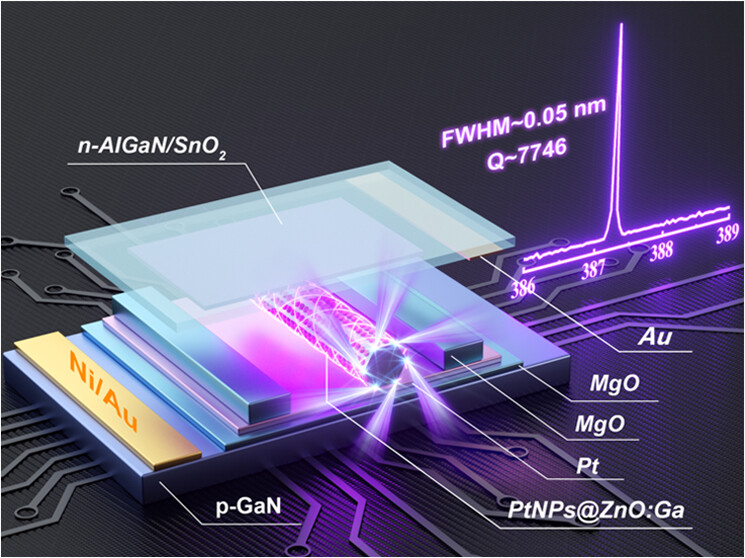
High Q-Factor and Low Threshold Electrically Pumped Single-Mode Microlaser Based on a Single-Microwire Double-Heterojunction Device
Jul. 21 , 2024photonics1
Abstract
The realization of micro/nanosized electrically pumped laser diodes, which show unique advantages including minimized footprint, ultralow threshold, energy-efficiency, and single-frequency characteristics, is hoped to feature as an indispensable unit in optoelectronic and photonic integrated circuits. Herein, we present a single-mode microlaser diode driven by electricity. This diode comprises an n-type AlGaN film coated with a SnO2 nanolayer, Pt nanoparticle-modified ZnO microwire via Ga impurity (PtNPs@ZnO:Ga MW), Pt/MgO bilayer, and a p-GaN substrate. The device demonstrates distinct double-heterojunction (n–n–p) characteristics, enabling it to lase at 387.3 nm. The line width is tremendously reduced to about 0.05 nm, yielding a laser’s quality (Q)-factor approaching 7746. The carefully designed double heterostructure allows one to achieve superinjection of current, accompanied by the efficient confinement of injected charge carriers and photons in the MW cavity. As the laser is modified using PtNPs with specific dimensions, dynamic modulation of lasing modes ranging from multimode to single-mode operation is achieved. Such a methodical design and assembly of a double-heterojunction microlaser device could open up new technological avenues for constructing high-performance single-mode microlaser diodes upon an electrical pump. We expect that this research will advance the development of single-mode microlasers with the desired performance for robust integrated optoelectronic applications.
This publication is licensed under the terms of your institutional subscription. Request reuse permissions.
The development of densely packed chip-scale microlaser diodes with high monochromaticity, narrow line width, low threshold, and compact size has garnered increasing attention due to their significant potential applications in on-chip optical communication, optoelectronic or photonic interconnection, high-resolution laser spectroscopy, medical imaging, ultradense information storage, and other fields. (1−8) While conventional III–V/II–VI inorganic semiconductors, organic materials, perovskites, and similar materials attaching small volume, well-established crystalline quality, excellent transport properties, naturally configured microcavities, easy integration, and superior optical gain characteristics, they are being explored for the construction of low-dimensional micro/nanolasers. (9−14) However, the larger size of the laser cavities often leads to multimode lasing emissions across a wide spectral range, resulting in temporal pulse broadening and false signaling because of relatively high group-velocity dispersion. (15−17) In recent years, various techniques and projects have been brought forward to manipulate laser modes and achieve a single-mode operation. These approaches include utilizing parity-time symmetry, using the Vernier effect, incorporating foreign distributed Bragg reflectors (DBR) or distributed feedback (DFB) cavity structures, and reducing the microcavity dimensions beyond the free space range of multimode operation. Most of these demonstrations have primarily focused on optically pumped systems. (3,16,18−21) With regard to practical applications, the advancement of microlaser devices demonstrating low noise, high monochromaticity, long coherence length, and high output power under electrical pumping is increasingly desired and must be pursued. To date, schemes for properly designing microlaser devices that satisfy the requirements of optical microcavities, optical confinement, efficient injection into the charge-carrier depletion layer, and other factors for electrical pumping are still relatively immature, with some shortcomings.
With the advancement of optoelectronic device miniaturization and various advantages, such as low energy consumption, advanced design, compact structure, and high reliability, individual lasing sources must be scaled down and integrated into small areas or volumes to a microscale or even a nanoscale. (13,22−24) The construction of laser devices, typically carried out through high cost, high-temperature vacuum processing, and rigid substrates, has become increasingly complex, time-consuming, and expensive. (15,25−28) In essence, achieving high-performance micro- and nanolasers upon electrical pumping remains challenging, primarily due to several drawbacks: (i) Significant nonradiative loss occurs at high carrier density levels necessary for population inversion; (29,30) (ii) small cavities inherently possess high electrical resistance; (25,31) (iii) resistant heat loss is generated within metal/semiconductor and p–n junction region; (32) (iv) lasing suppression can be induced by conductive functional layers in electroluminescence (EL) devices; (33) and (v) substantial losses occur around the resonant cavity due to high-level current injection and other factors. (34,35) These perspectives pose substantial obstacles to further advancement of realistic microlaser devices. Therefore, it is imperative to propose rational laser structures. Additionally, a feasible strategy should be developed experimentally, aiming to simultaneously achieve microcavity mode engineering and single-mode lasing emission under both optical and electrical excitation.
In this study, a novel device structure comprising an n-type AlGaN film covered by a SnO2 dielectric nanolayer, Pt nanoparticle-modified ZnO microwire via Ga-dopant (PtNPs@ZnO:Ga MW), Pt/MgO nanolayers, and a p-type GaN substrate was well established. The device exhibited well-defined double-heterojunction characteristics, which enabled lasing at a wavelength of 387.3 nm in the UV region and a relative bandwidth of 0.05 nm upon electrical pumping. The carefully fabricated single MW double-heterojunction properties were systematically examined. In the device, the insertion of a bilayered Pt/MgO film into ZnO:Ga/GaN allowed to engineering the electronic structure and carrier recombination path, thus achieving efficient integration of the charge-carrier recombination area, laser gain material, and optical microcavity in the PtNPs@ZnO:Ga MW. The use of a highly conductive n-AlGaN film as an efficient electron-injection layer could boost the injection and confinement of electrons within the PtNPs@ZnO:Ga MW, which contributes to population inversion. Apart from the enhancement of its electrical conductivity, surface modification using PtNPs with specific sizes enables to manipulate the lasing modes of the ZnO:Ga MW microlaser, ranging from multimode to single-mode operation. Especially noteworthy is that the exceptional high reflectivity in the UV region, provided by the top AlGaN/SnO2 bilayer and bottom Pt/MgO/GaN films serving as reflective cavity surfaces, allowed further boosting of the device performance. This arrangement aids in reducing microcavity loss in the PtNPs@ZnO:Ga MW, thereby enhancing the light-emitting output characteristics. In one word, the designed single MW double heterojunction not only optimizes optical-field confinement but also enhances carrier injection efficiency at the n–n–p junction and confines carriers to the PtNPs@ZnO:Ga MW active region. As a result, the laser structure is well suited for achieving lasing emission that satisfies both optical and electrical requirements for the microlaser diodes pumped by electricity. These configurations show promise for electrically pumped lasers and facilitate further advancements in achieving adequate current density and significant gain. This research demonstrates a viable paradigm for the design and fabrication of electrically pumped single-mode microlaser diodes.
Experimental Section
Fabrication of ZnO:Ga Monocrystalline Structures
The product of one-dimensional ZnO:Ga single crystals was fabricated via a catalyst-free chemical vapor deposition (CVD) method. (36,37) A mixture of high-purity ZnO, Ga2O3, and graphite (C) powders (∼99.9%) at a specific ratio of 9:1:10 was preferred to serve as the precursor. This precursor mixture was situated in a ceramic boat. To collect the resulting products, a clean Si wafer was positioned atop the precursor. Subsequently, the boat was transferred to a horizontal quartz tube furnace. The sample growth temperature was maintained at 1200 °C. Throughout the synthesis process of sample fabrication, a mixture of argon (Ar, ∼125 sccm) and oxygen (O2, ∼5 sccm) served as carrier and protective gas, respectively, was flowed into the quartz tube furnace. Following approximately 1 h of reaction time, the ZnO:Ga MWs grew vertically around the Si film. The cross-sectional sizes of the one-dimensional MWs were in the range of 500 nm to 50 μm, with lengths of up to 2.0 cm.
Preparation of PtNPs@ZnO:Ga MWs
The precursor Pt nanolayers were deposited on the ZnO:Ga samples using simplified magnetron-sputtering equipment. An annealing treatment of the MWs coated with a Pt nanolayer via specific thickness was performed in a tube furnace at 400 °C, as illustrated in Figure S1a. It is evident that PtNPs with physically dispersed and relatively uniform sizes were successfully prepared on the surfaces of ZnO:Ga, thus yielding a hybrid structure of individual PtNPs@ZnO:Ga MWs. Consequently, a ZnO:Ga wire coated by PtNPs was effectively achieved, as shown in Figure S1b. Varying the sputtering time, the thickness of precursor Pt nanolayers can be changed, thus allowing tuning of the three-dimensional sizes of hemispheric PtNPs on ZnO:Ga MWs. As can be seen in Figure S1c, the cross-sectional dimensions of the Pt hemispheric structures were tested to about 140 nm on average.
Diode Design and Fabrication
A schematic description and optical image of the double-heterojunction microlaser diode are shown in Figures S2 and S3, respectively. In the microlaser diode, the high-conductivity n-type AlGaN film prepared on double-polished sapphire, which was used as an electron-injecting layer, was commercially available; while the p-type GaN layer employed as a hole supplier was also commercially purchased. The related electrical parameters of AlGaN and GaN films are available in Table S1. The as-designed double heterostructure light-emitting/lasing device was manufactured via a simple bottom-up process as follows: (i) A Ni/Au bilayer (50/60 nm) was fabricated on a clean p-GaN substrate using a deposited with the vacuum thermal evaporation technique. After annealing treatment, the Ni/Au film was utilized as the anode. (ii) A MgO nanolayer of ∼10 nm was evaporated on the blank GaN substrate using metal–organic chemical vapor deposition (MOCVD) system. (iii) Afterward, a Pt nanolayer of ∼10 nm was evaporated on the MgO nanolayer using MOCVD. (iv) A rectangular hole via MgO microlayers was prepared on the Pt nanolayer. The depth of the rectangular hole was derived to be about 5.0 μm. In the device, the prepared MgO microlayers acted as insulating media, enabled to avoid the direct contact between the top AlGaN and the underlying GaN film. (v) The pre-prepared PtNPs@ZnO:Ga wire was situated on the blank area of the Pt nanolayer. (vi) Finally, an n-AlGaN substrate (Au electrode) covered with a SnO2 nanolayer was placed on the PtNPs@ZnO:Ga MW, which served as the cathode and electron-transporting layer.
Materials and Device Characterization
The morphology and elemental distribution of CVD-fabricated ZnO:Ga MWs, uncoated and coated with PtNPs, were characterized by energy-dispersive X-ray spectroscopy (EDS) associated with scanning electron microscopy (SEM). X-ray diffraction (XRD) of the products was examined via an X-ray diffractometer equipped with Cu Kα radiation (λ = 1.5406 Å). A field-emission transmission electron microscope (TEM) (Tecnai G2 F20) operated at 200 kV was used to research the crystal quality and structure of the as-synthesized samples. Photoluminescence (PL) measurements of the samples, including a ZnO:Ga wire without and with PtNP coating, a GaN layer, and an AlGaN layer, were carried out through a 266 nm continuous-wave (CW) laser combined with a spectrometer (LABRAM-UV Jobin Yvon). Lasing characterization of the single ZnO:Ga MW uncoated and coated with PtNPs and the individual PtNPs@ZnO:Ga MW unsandwiched and sandwiched into the carefully fabricated double-heterojunction device was measured using a 266 nm femtosecond (fs) pulsed laser (pulse duration of 150 fs, repetition rate of 1000 Hz). The light output was recorded using an optical multichannel analyzer (Princeton, Acton SP2500i). The electrical properties of the device were determined using a Keysight semiconductor device analyzer (Keithley, B1500A). EL characterization was tested via a charge-coupled device (CCD) camera (1024BR-PIXIS series CCD camera, Princeton Instruments). Besides, the reflectance spectra were examined by using an UV–visible (VIS)–near-infrared (NIR) spectrophotometer (UV-3600 Plus). The output power of the laser was recorded by using an OPHIR Nova II power meter. Polarization properties were determined by rotating a rotatory polarizer through the microscope objective with the polarizer mounted on the top surface of the device. All of the measurements were performed at room temperature.
Results and Discussion
Morphology and Structural Characterization
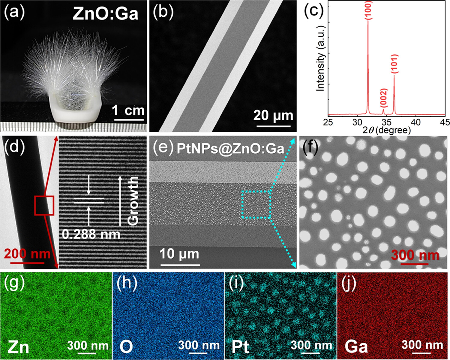
Using a simple CVD via a catalytic-free approach, the product of wire-like ZnO:Ga structures was successfully synthesized. An optical photograph taken by a digital camera is shown in Figure 1a, which reveals that the ZnO:Ga wires could be collected individually around the precursor Si substrate. As depicted in the figure, the prepared wires can reach 2.0 cm in average. Figure 1b shows an SEM graph of a ZnO:Ga MW, illustrating hexagon-shaped outlines, sharp edges, and atomically smoothed surfaces. The diameter of the wire is about 20 μm. To examine the crystalline quality, a typical XRD measurement of the samples was characterized. Figure 1c reveals that the strongest diffraction positioning at around 31.76, 34.45, and 36.25° is, respectively, contributing to the (100), (002), and (101) crystal planes. The ZnO:Ga samples obtained via CVD exhibit a hexagonal wurtzite structure with impeccable crystalline quality. (38,39) TEM was employed to exploit the interior electronic structures of a ZnO:Ga wire. The resulting TEM in Figure 1d confirms that the wire exhibits a consistent profile with straight and smooth boundaries. Furthermore, a selected sharp edge of the ZnO:Ga wire was examined by using high-resolution TEM, which reveals clear lattice fringes. The spacing of these lattice fringes was measured to be about 0.288 nm. This value is visibly larger than that of the intrinsic ZnO single crystal (∼0.260 nm), suggesting that the Ga doping allows to expanse the ZnO lattice because of the substitution of the Ga atom for Zn. (25,40)
Figure 1
Figure 1. Characterization of CVD-grown ZnO:Ga MW uncoated and coated with Pt nanoparticles. (a) Photograph of the ZnO:Ga sample. (b) SEM illustration of the ZnO:Ga wire. (c) XRD analysis of the ZnO:Ga wire. (d) Low-resolution TEM figure of the ZnO:Ga wire via a 200 nm diameter (left), and the high-resolution TEM shows that the lattice spacing is evaluated to approximately 0.288 nm (right). (e) SEM exhibition of the ZnO:Ga wire coated with PtNPs. (f) Magnified SEM of the deposited PtNPs. (g–j) EDS mapping results of a PtNPs@ZnO:Ga wire, revealing the distribution of Zn, O, Pt, and Ga elements.
It is well known that the sample of PtNPs featuring excellent metallic nanostructures has been utilized to engineer the optical/electrical and optoelectronic properties of low-dimensional wide band gap semiconductors. Herein, PtNPs with controlled sizes, well dispersed, and uniformly fabricated distribution were deposited on ZnO:Ga MWs by combining thermal evaporation and annealing treatment. The preparation process can be found in the Experimental Section. Figure 1e shows an SEM exhibition of a PtNP-coated ZnO:Ga MW. The surface-coated PtNPs are further enlarged in Figure 1f. In addition, by changing the fabrication conditions including sputtering time, annealing temperature and time, and others, the product of noble-metal Pt with different shapes, sizes, and gap distances can be fabricated on the ZnO:Ga MW. A random area of the PtNPs@ZnO:Ga wire was selected to characterize its EDS mapping, which is shown in Figure 1g–j. Apart from the resulting elements of Zn, O, and Ga, the circular Pt with well-defined boundary is clearly seen. Owing to the surface tension and recrystallization of the annealing treatment, PtNPs with hemiellipsoid-shaped structures can be created on the outside surfaces of CVD-fabricated ZnO:Ga wire, rather than surface doping. (3,41) Therefore, the sample of ZnO/Ga MWs coated with PtNPs was achieved.
PtNPs@ZnO:Ga MW Single-Mode Microlaser upon Optical Pumping
Previous studies have reported that CVD-synthesized ZnO:Ga MWs with hexagon-shaped structures allowed the construction of typical whispering-gallery-mode (WGM) microlasers. The lasing characteristics, which contained lasing modes, thresholds, and Q-factors, are highly dependent on the microcavity sizes. Particularly for the laser modes, the larger size of the microcavity can result in much more lasing modes. (16,36) Unfortunately, the absence of mode competition mechanism enabled to produce multimode laser emissions, which would give rise to serious group-velocity dispersion, as well as temporal-pulse widening and fake signals. (15,17,42) The incorporation of PtNPs with specific sizes has been proposed to engineering lasing modes of large-size ZnO:Ga MWs (cross-sectional diameter ≥1.0 μm) both upon electrical and optical pumping due to their plasmonic response and superabsorption characteristics in the UV region. A workable operation upon electrical pumping has always been one of the core scientific and technical issues concerned in the development of single-mode microlaser devices. Actually, the concept of electrically pumped single-mode microlaser diodes is remarkably distinct. The integration of the small-size gain medium into a rational device configuration enables to achieve single-mode lasing upon both electrical and optical excitation remains challenging. In this regard, a bottom-up vertical structure, which comprises an AlGaN/SnO2 bilayer (top mirror, electron-transporting layer), a PtNPs@ZnO:Ga MW (active medium and optical microcavity), and Pt/MgO/GaN layers (bottom mirror, and hole supporting source), was devised. The combination of the top AlGaN/SnO2 bilayer and bottom Pt/MgO/GaN layers can serve as DBRs to manipulate the lasing characteristics of a well-defined PtNPs@ZnO:Ga wire microlaser.
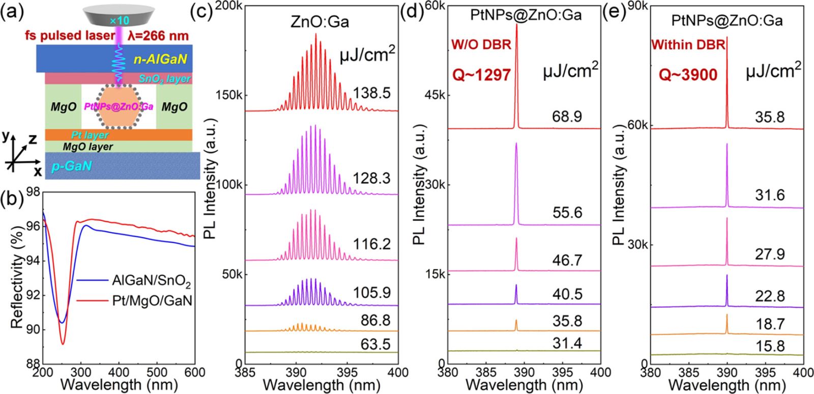
A schematic of the microcavity laser is depicted in Figure 2a. In a hexagonal ZnO:Ga microstructure, light can circulate around the inside walls to form a typical WGM cavity within the cross section through total internal reflection (TIR). According to the Fresnel formula, the equation for WGM resonance can be deduced, which is expressed as (36,43)
where n is the refractive index for the resonant wavelength (λ) and the integer N is the lasing mode number. The WGM equation is not valid as the cavity size is smaller than the wavelength. If the ZnO:Ga microcavity is located in some other media instead of air, the refractive index in the above equation should be substituted by the relative refractive index nr = nZnO:Ga/nout. Here, nZnO:Ga and nout are the refractive indices of the hexagonal ZnO:Ga MW and the surrounding environmental media. The WGM equation can be written as (36,43)
Figure 2. Lasing-emission characterization of a PtNPs@ZnO:Ga MW, which was unsandwiched and sandwiched into the as-designed DBR-like structure upon optical pumping. (a) Cross-sectional schematic of a PtNPs@ZnO:Ga MW sandwiched between the AlGaN/SnO2 bilayer (top DBR) and the Pt/MgO/GaN layers (bottom DBR). (b) Reflectance spectra of the AlGaN/SnO2 bilayer and Pt/MgO/GaN films. (c) Pump-fluence-dependent PL spectra of a hexagon-shaped ZnO:Ga MW, with the pumping fluence ranging from 63.5 to 138.5 μJ/cm2. (d) Pump-fluence-dependent lasing-emission spectra of a single PtNPs@ZnO:Ga MW, with the pumping fluence ranging from 31.4 to 68.9 μJ/cm2. (e) As the PtNPs@ZnO:Ga MW was sandwiched into the AlGaN/SnO2–Pt/MgO/GaN DBR-like cavity structure, lasing-emission spectra were also collected by increasing the pumping fluence ranging from 15.8 to 35.8 μJ/cm2.
The second term on the right-hand side of the equation denotes the total phase shift in the six interfaces, where nri denotes the refractive index of the corresponding medium.
The corresponding Q-factor of WGM microcavity has been calculated as follows: (44,45)
??=????????????/42??(1−????/2)sin(2????)
(3)
In an m-faceted polygonal cavity, the Q-factor is given by where m is the number of facets, n is the refractive index of the medium, D is the diameter of the circumscribed circle of the polygon, and R is the reflectivity of the facet mirrors. In this regard, the nanolayers of SnO2 and MgO were introduced to surround the sandwiched PtNPs@ZnO:Ga MW due to their low-dielectric intrinsic quality. Therefore, the optical losses at the AlGaN/ZnO:Ga and ZnO:Ga/GaN interfaces could be significantly reduced.
The influence of the AlGaN/SnO2 bilayer and the underlying Pt/MgO/GaN films on the optical properties of the sandwiched PtNPs@ZnO:Ga MW was researched. First, the reflectance spectra of the AlGaN/SnO2 bilayer and Pt/MgO/GaN films were measured using an UV–vis–NIR spectrophotometer (UV-3600 Plus), which exhibit maximum reflectivity of 96.1 and 96.4%, respectively, in the UV spectral band (see Figure 2b).
The broad high-reflectivity region of the stopband, ranging from 350 to 410 nm, includes the overall lasing emission of the ZnO:Ga MW. Consequently, strong optical confinement within the PtNPs@ZnO:Ga MW microcavity could be boosted with the aid of the top and bottom reflective mirrors. The speculation was further tested. PL measurements depending on the pumping fluence were conducted using a testing system via a 266 nm fs pulsed laser. (27,46) The schematic view of the measurement equipment and optical path is shown in Figure S4. A hexagon-shaped ZnO:Ga MW with a diameter of about 20 μm was pumped optically. The resulting PL spectra are shown in Figure 2c. At a low pumping fluence of 63.5 μJ/cm2, a weak and broad spontaneous emission (SP) located at ∼392 nm can be observed. When the pumping fluence is increased to 86.8 μJ/cm2, several sharp peaks emerge over the broad emission band. On further increasing the pumping fluence to 138.5 μJ/cm2, the PL spectra are dominated by a series of sharp peaks. At the same time, the emission intensity is significantly increased, suggesting that typical WGM lasing behavior with multimode was achieved.
As previously reported, PtNPs via specific dimensions enabled to engineering lasing modes and then realizing single-mode operation of a ZnO:Ga MW-based microlaser. (3) By combining magnetron sputtering and annealing treatment, a hybrid structure made of the ZnO:Ga MW covered with PtNPs was constructed. The cross-sectional diameter of deposited PtNPs was evaluated on average to be about 140 nm. Then, the ZnO:Ga MW coated with PtNPs (average diameter ∼140 nm) was optically pumped. PL spectra in Figure 2d exhibit that the PtNPs@ZnO:Ga MW reveals a weak and broad-band spontaneous radiation centering at 389 nm with a line width of 10.6 nm as the pumping fluence is less than 31.4 μJ/cm2. As the pumping fluence increases to 35.8 μJ/cm2, a sharp spectrum line was observed at 389 nm. Upon further increasing the pumping fluence to 68.9 μJ/cm2, the PL spectrum is dominated by a single sharp peak with a line width of 0.3 nm. Moreover, the lasing intensity significantly increased, suggesting the transformation of excitonic recombination from spontaneous emission to stimulated emission. Notably, only one lasing peak survived in the PL spectra, indicating that the well-fabricated PtNPs@ZnO:Ga wire with a specific size can be used to construct a single-mode microlaser device. Additionally, the lasing-emission characteristics of the ZnO:Ga MW uncoated and coated by PtNPs are depicted in Figures S5 and S6. Therefore, the PtNPs@ZnO:Ga MW could be utilized to construct single-mode microlaser devices upon optical pumping.
As the PtNPs@ZnO:Ga MW was sandwiched into the carefully fabricated AlGaN/SnO2 bilayer and Pt/MgO/GaN substrate, similar lasing measurements were also performed. In Figure 2e, as the sample was optically excited at 35.8 μJ/cm2, a narrow sharp peak appears at 390 nm with a line width of 0.1 nm. In addition, the PL emission intensity increases dramatically, suggesting the successful observation of a single-mode lasing operation. The Q-factor values of the PtNPs@ZnO:Ga MW unembedded and embedded within the DBR-like structure were evaluated based on the formula Q = λ/δλ, wherein the parameters λ and δλ represent the lasing wavelength and line width of the spectra, respectively. (8,43) The Q-factor value of the PtNPs@ZnO:Ga MW within the DBR-like structure is determined to be 3900, which is considerably larger than that of the unsandwiched sample (Q-factor ∼1297). Conclusively, the constructed DBR-like cavity structure is conducive to boosting the monochromatic characteristics of the PtNPs@ZnO:Ga MW-based single-mode laser.
The influence of the AlGaN/SnO2–Pt/MgO/GaN DBR-like structure on the lasing features of the PtNPs@ZnO:Ga MW-based single-mode microlaser was studied at room temperature. Figure 3a (blue solid line) shows that the resulting PL spectrum of the unsandwiched PtNPs@ZnO:Ga MW exhibits a broad spectral profile peaking at 376 nm. The primary peak aligns consistently with the room-temperature band-edge emission of ZnO:Ga. (3) Upon integration of PtNPs@ZnO:Ga MW into the AlGaN/SnO2–Pt/MgO/GaN DBR-like structure, the PL peak wavelength undergoes a red shift to 389 nm, possibly due to self-absorption effects within the designed DBR-like structure. Furthermore, the PL spectrum of the embedded PtNPs@ZnO:Ga MW distinctly illustrates a set of parabolic-like dispersions of optical cavity modes, likely arising from oscillations between the top and bottom facets of the constructed AlGaN/SnO2 and Pt/MgO/GaN DBRs. (47) A corresponding demonstration of the mode dispersions is shown in Figure S7. Lasing spectra of the PtNPs@ZnO:Ga MW within the AlGaN/SnO2–Pt/MgO/GaN DBR-like cavity structure and without it are shown in Figure 3b for comparison at a pumping fluence of 35.8 μJ/cm2. Notably, the AlGaN/SnO2–Pt/MgO/GaN DBR-like structure enables the boost of output intensity of single-mode lasing of the PtNPs@ZnO:Ga MW-based microlaser by 9-fold.
Figure 3
Figure 3. DBR microcavity effect on the single-mode lasing characteristics of a PtNPs@ZnO:Ga sample. (a) Comparison of the PL spectra obtained of a PtNPs@ZnO:Ga MW sandwiched into the carefully fabricated AlGaN/SnO2–Pt/MgO/GaN DBR-like cavity or not. (b) Lasing spectra of the PtNPs@ZnO:Ga sample within the AlGaN/SnO2–Pt/MgO/GaN DBR-like cavity or not were given for comparison when pumped at a fluence of 35.8 μJ/cm2. (c) Calculated cavity mode numbers (middle panel) and refractive indices (top panel) corresponding to the lasing spectra of PtNPs@ZnO:Ga MW sandwiched into the DBR-like cavity structure or not. (d) Comparison of the integrated PL intensity of PtNPs@ZnO:Ga MW within or without the AlGaN/SnO2–Pt/MgO/GaN DBR-like cavity, concerning the pumping fluence. Numerical simulation depicts the distribution of optical-field intensity patterns within the hexagon-shaped cross section of (e) the n-PtNPs@ZnO:Ga MW/Pt/MgO/p-GaN emission device structure and (f) the n-AlGaN/SnO2/n-PtNPs@ZnO:Ga MW/Pt/MgO/p-GaN emission device structure.
Theoretical calculation was conducted through a simple plane-wave model for WGM optical microcavity, (10,48) which aimed to illustrate the relationship among the lasing mode number N, refractive index n, and lasing-emission peak λ of the PtNPs@ZnO:Ga MW unsandwiched and sandwiched within the DBR-like structure. Evidently shown in Figure 3c, the lasing mode number of the PtNPs@ZnO:Ga wire integrated within the AlGaN/SnO2–Pt/MgO/GaN DBR-like structure is estimated to be about 154, which is smaller than that of the unsandwiched MW (mode number ∼155). The variations in the integrated PL intensity versus the various pump-fluence values are plotted in Figure 3d. As the pumping fluence increases, the intensity of spontaneous radiation exhibited an insensible increase below the corresponding threshold and then increases sharply above the threshold. The threshold value of the PtNPs@ZnO:Ga MW sandwiched within the AlGaN/SnO2–Pt/MgO/GaN DBR-like cavity structure is 16.5 μJ/cm2, which is obviously lower than that of the unsandwiched sample (Pth ∼ 32.6 μJ/cm2). These findings suggest that the incorporation of an as-designed AlGaN/SnO2–Pt/MgO/GaN DBR-like cavity structure can boost the single-mode lasing performances of a PtNPs@ZnO:Ga MW microlaser, including a lower lasing threshold, a higher lasing output intensity, and a larger Q-factor. And, the boosted lasing characteristics could be derived by raising the relative refractive index on the basis of the TIR at the top and bottom boundaries of the hexagon-shaped ZnO:Ga wire.
Prior studies have indicated that hexagon-shaped ZnO:Ga micro- and nanostructures can support WGM microcavities due to near-perfect full feedback at the ZnO:Ga/air boundaries. Utilizing the finite-difference time domain (FDTD), we simulated the optical-field confinement within the cross section of a PtNPs@ZnO:Ga wire laser device. In this simulation, the cross-sectional diameter of the used ZnO/Ga wire was 20 μm. Effective refractive indices of the ZnO:Ga wire, air, AlGaN/SnO2 films, and Pt/MgO/GaN films were assumed to be 2.35, 1.0, 1.95, and 2.0, respectively. We also computed the optical-field distributions within the cross section of the PtNPs@ZnO:Ga MW, which was modeled on a Pt/MgO/GaN substrate. As illustrated in Figure 3e, the simulation results show that the regular hexagon-shaped PtNPs@ZnO:Ga MW can form WGM-type cavity. In Figure 3f, when the PtNPs@ZnO:Ga MW was integrated into the carefully designed AlGaN/SnO2–Pt/MgO/GaN DBR-like cavity structure, the optical-field distribution was recalculated. Notably, a transition from WGM to Fabry–Pérot (F–P) mode was observed, likely due to the external microcavity. In conclusion, the construction of a typical AlGaN/SnO2–Pt/MgO/GaN DBR-like cavity structure enables strong optical confinement. In this case, it can confine light more effectively and reduce light leakage, thus achieving the enhancement of a single-mode lasing operation of the PtNPs@ZnO:Ga MW.
The creation of p–n junction lasers was the seed from which semiconductor optoelectronics started to grow. Recently, the construction of a p–n heterojunction with a combination of different semiconductors and carefully engineered band structures is considered to be an intelligent approach in promoting device performances by attaining charge redistribution and manipulation at the interfaces. Compared with single-component materials, such heterojunction provides unique physical, mechanical, and chemical properties due to charge interactions, crystal defects, and lattice strain created at interfacial junctions. (49,50) Generally, heterojunctions exhibit extremely high injection efficiencies. However, the electron and hole pairs injected into the depletion region at the required high concentrations for lasing often diffuse away, diminishing the available carriers for light emission into the cavity. These challenges pose limitations on achieving high-performance EL devices, especially in the context of electrically driven lasers. In contrast to a single p–n heterojunction, a double heterojunction offers the advantage of surrounding the depletion region with wider band gap materials, effectively confining the electron–hole pairs to the junction. Moreover, double heterojunction facilitates efficient injection of the charge carriers, lowering threshold current, and efficient suppression of Joule heating, thereby enabling to boost light-emitting diode (LED)/laser performances before encountering thermal constraints. (49,51) Therefore, the development of a completely new device structure is imperative for realizing high-performance electrically driven single-mode microlaser diodes.
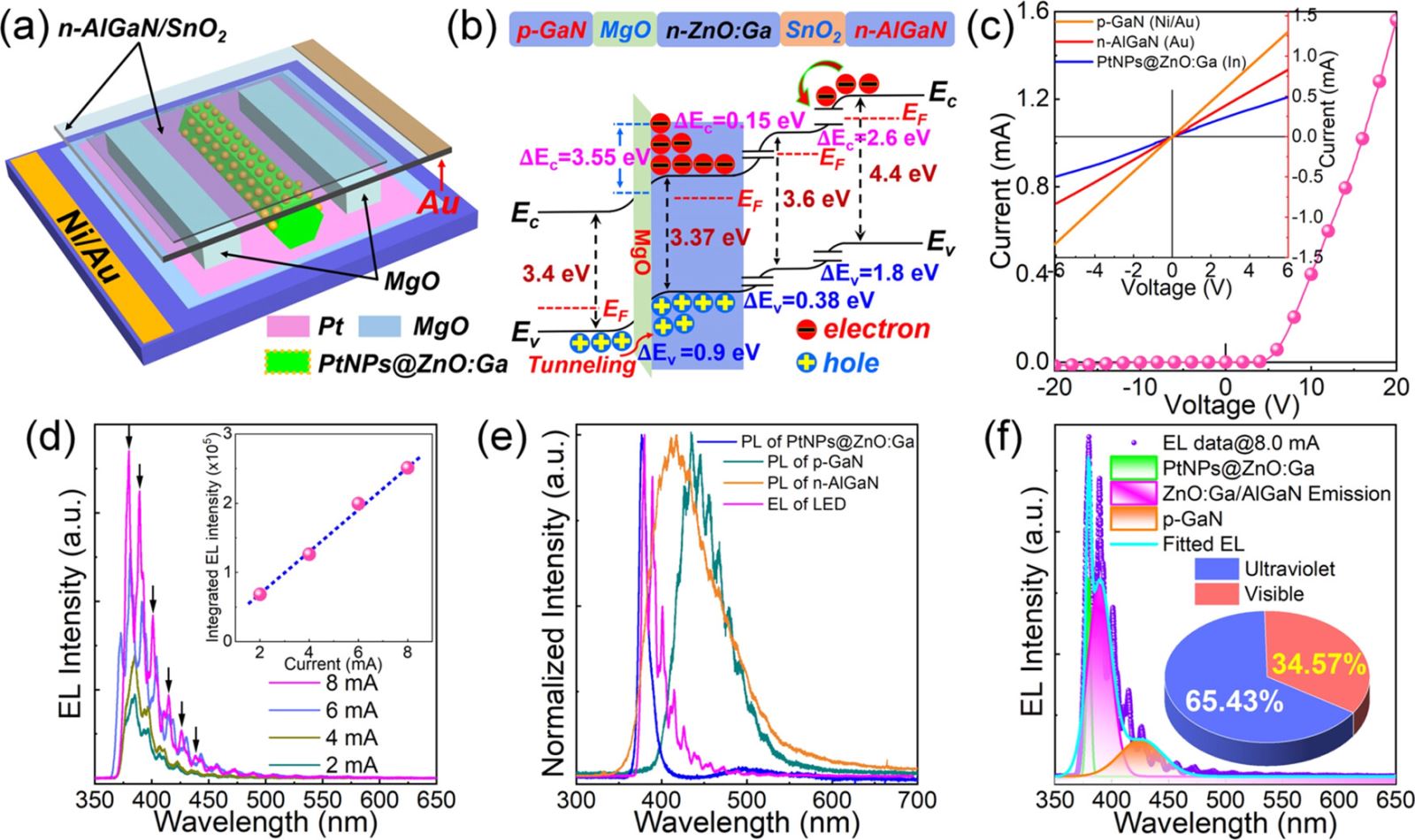
A novel double heterostructure was created in the current study, consisting of an n-type AlGaN layer for electron transport, a PtNPs@ZnO:Ga MW acting as an active medium and optical microcavity, Pt/MgO double layers for interface engineering, and a p-type GaN layer for hole supply (Figure 4a). The design concept was illustrated by investigating the carrier transport and recombination mechanism of the device by using the energy band diagram under forward bias conditions. The relating energy band diagram is depicted in Figure 4b, wherein the electron affinities ψZnO:Ga, ψMgO, ψSnO2, ψGaN, and ψAlGaN are 4.35, 0.80, 4.50, 4.20, and 1.90 eV, respectively; while the energy band gaps (Eg) of ZnO:Ga, MgO, SnO2, GaN, and AlGaN are 3.37, 7.60, 3.60, 3.40, and 4.40 eV, respectively. (2,3,14,52,53) The conduction-band offset (CBO) and valence-band offset (VBO) toward the ZnO:Ga/MgO and GaN/MgO heterointerfaces were evaluated to be 3.55 and 0.9 eV, respectively. As the device was forward biased electrically, most of the applied voltage was directed onto the MgO layer because of its insulating character, causing a bending in the energy band of MgO. At the same time, the effective barrier of the VBO near the GaN/MgO interface is notably reduced. In this case, the smaller VBO allowed holes at the GaN layer to tunnel through the GaN/MgO interface and then enter into the ZnO:Ga MW side. Conversely, the presence of the MgO interlayer effectively prevents electron transporting from ZnO:Ga to the GaN region. (2,14) Similarly, the CBO and VBO at the ZnO:Ga/SnO2 interface are calculated to be about 0.15 and 0.38 eV, respectively; while the CBO and VBO at the SnO2/AlGaN interface are found to be 2.6 and 1.8 eV, respectively. This suggests that injected electrons can be efficiently confined within the MW due to the significant electron barrier at the double heterointerfaces. For the carefully designed double heterojunction driven electrically in the forward-biasing region, drifting of the injected electrons from the PtNPs@ZnO:Ga MW to the underlying GaN substrate was principally blocked by the MgO intermediate layer; however, the tunneling of holes through the PtNPs@ZnO:Ga/GaN interface dominated the overall current of the device. Upon the biased forward voltage reaching a certain value, holes from the GaN film and electrons from the AlGaN film are simultaneously injected into the MW active region, where efficient radiative recombination of the confined charge carriers occurs.
Figure 4
Figure 4. Characterization of the constructed double heterostructure light-emission device. (a) Three-dimensional architecture of the double-heterojunction device. (b) Energy band architecture of the n-AlGaN/SnO2/n-PtNPs@ZnO:Ga MW/Pt/MgO/p-GaN double heterostructure device operated upon forward-biasing conditions. (c) I–V characteristic curve of the experimentally fabricated single MW double-heterojunction device. Inset: I–V curves of the Au electrode in contact with the n-AlGaN film, the metallic Ni/Au electrode in contact with the p-GaN film, and the In electrode in contact with the PtNPs@ZnO:Ga MW. (d) Current-guided EL spectra. Inset: the current-dependent integrated EL intensity of the device. (e) PL spectra of a PtNPs@ZnO:Ga MW, a GaN layer, and an AlGaN layer along with the normalized EL emission spectrum (∼8.0 mA). (f) Gaussian fitted EL spectrum at 8.0 mA. The inset image illustrates the contents of the UV and visible light components.
The volt–ampere characteristics via the current–voltage (I–V) curve recorded from the fabricated device, depicted in Figure 4c, show a standard rectification and a threshold voltage of about 4.0 V. The device exhibits a forward current of 1.56 mA at 20 V and a leakage current of 0.016 mA at −20 V, resulting in an estimated rectification ratio of 98. The linear properties in terms of I–V curves for the Au layer on the n-AlGaN film and the Ni/Au bilayer on the p-GaN film, as shown in the inset of Figure 4c, indicate good Ohmic contacts at both the n- and p-type electrodes. Furthermore, the I–V curve of the PtNPs@ZnO:Ga MW with the In electrode also exhibits linear behavior, as shown in the inset of Figure 4c, confirming that the rectifying property arises from the double-heterojunction device. Besides, the electrical and optical properties of an individual ZnO:Ga MW uncoated and coated by PtNPs are exhibited in Figure S8. Notably, the electrical properties of the device surpass those previously reported, including lower turn-on voltage, higher injection current, and relatively lower leakage current. Figure 4d illustrates the EL spectra of the device, measured by the current varying from 2.0 to 8.0 mA. At 2.0 mA, only a broad emission peaking at around 384.5 nm is observed, and the spectral line width is measured to about 23.5 nm at full width at half-maximum (fwhm). As the driving current increases to 8.0 mA, some quasi-equidistant oscillating peaks with equally spaced line width emerge on the broad-band spectra (as denoted by arrows), resulting in high-brightness and narrow-band pure UV EL. The positions of the obtained EL peaks remain nearly unchanged as the driving current increases. The excellent characteristics of the EL spectra suggest the formation of a perfect microcavity, which originated from the hexagon-shaped PtNPs@ZnO:Ga MW. In the inset of Figure 4d, the relationship between the integrated EL intensity versus the driving current exhibits approximatively linear, indicating that UV EL is dominated by radiative recombination occurring in the PtNPs@ZnO:Ga MW active zone.
The EL emission mechanism was studied. First, optical properties of the PtNPs@ZnO:Ga wire, GaN layer, and AlGaN layer were measured using a 266 nm CW laser at room temperature. Figure 4e exhibits the normalized intensities of the PtNPs@ZnO:Ga PL, GaN film PL, and AlGaN film PL, and the EL spectrum of the device, wherein the light emission peaking at 376.5 nm could be assigned to the PtNPs@ZnO:Ga sample (blue solid line). The solid green line characterized by a broad-band light emission positioning at 435.5 nm typically originated from radiative transition from the conduction band to the Mg-doping-related acceptor level in the p-GaN substrate. (41) Additionally, the broad-band UV EL light emission at 379.5 nm, which is observed in the as-fabricated LED, aligns well with the PL peak of the PtNPs@ZnO:Ga MW. In this case, it is concluded that UV EL emission of the carefully fabricated n-AlGaN/SnO2/n-PtNPs@ZnO:Ga MW/Pt/MgO/p-GaN double-heterojunction device primarily results from electron–hole recombination, which would occur in the PtNPs@ZnO:Ga MW active medium. The light-emitting regions, whether occurring at the ZnO:Ga/AlGaN or in the ZnO:Ga/GaN interfaces, can be effectively suppressed.
In order to explore the source of the EL spectra, the EL spectrum upon a forward input current of 8.0 mA underwent Gaussian fitting, as shown in Figure 4f. The analysis reveals three distinct sub-bands positioned at 379.5, 389.5, and 430.5 nm, respectively. Notably, the Gaussian curves aligned well with the experimental data. Making a comparison with the PL results, the UV light emission centering at around 379.5 nm was ascribed to the emission of well-fabricated PtNPs@ZnO:Ga samples. The obtained light emission at 389.5 nm was approximately linked to ZnO:Ga/AlGaN interfacial radiative recombination, involving electrons from the PtNPs@ZnO:Ga MW and holes from the n-AlGaN film. The emission band near 430.5 nm may stem from transitions within the p-GaN film. To measure the UV content of the device, the integral intensity of UV (<400 nm) and visible spectra (>400 and <700 nm) was calculated. (54) In the inset of Figure 4f, it is evident that the UV light content of the device is 65.43%, indicating a high level of UV light emission with considerable brightness. Hence, a well-defined double heterojunction could effectively integrate the charge-carrier recombination zone, laser gain medium, and optical microcavity within the PtNPs@ZnO:Ga MW. This enhances both the injection and confinement of electron–hole pairs within the MW active region, thus facilitating population inversion.
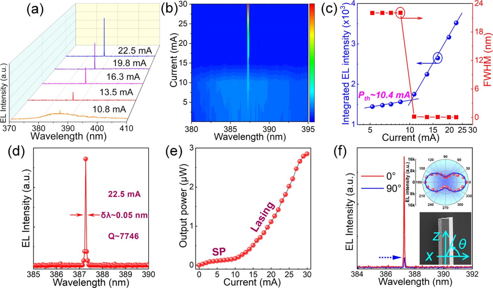
The experimentally constructed n-AlGaN/SnO2/n-PtNPs@ZnO:Ga MW/Pt/MgO/p-GaN double-heterojunction device was further examined under CW operation of current injection at ambient temperature. Varying the driven current, the collected EL spectra are depicted in Figure 5a. Upon reaching an input current of 10.8 mA, a sharp peak abruptly appears at 387.3 nm, overlaying the broad emission band. This suggests a transition of the excitonic recombination from spontaneous radiation to stimulated radiation. As the driven current varies to 22.5 mA, the spectral lines are principally determined by a group of sharp peaks, with the line width narrowed to 0.05 nm at fwhm. There is minimal variation in the profile shape and peak positions of the EL spectra as the driven current increased beyond 10.8 mA. Additionally, the broad-band EL background noise (spontaneous radiation) has been effectively suppressed. Notably, the presence of a single peak at high injection levels in the EL emission band indicates the realization of single-mode lasing action. Figure 5b presents the spectral map of the device with an increasing injection current, clearly depicting a narrow single-mode lasing emission.
Figure 5
Figure 5. Lasing characterization and polarization emission properties of the as-constructed electrically pumped n-AlGaN/SnO2/n-PtNPs@ZnO:Ga MW/Pt/MgO/p-GaN double-heterojunction diode. (a) EL spectra of the device under a driving current varying in the scope of 10.8–22.5 mA. (b) Spectral map of the EL spectra as a function of injecting current. (c) Changes in the integrated EL intensity and spectral line width in terms of the operating currents. The threshold current was extracted as 10.4 mA. (d) The fitted EL spectrum at 22.5 mA via Lorentz, the resulting line width is 0.05 nm, yielding a high Q-factor of 7746. (e) Variations in the output power in the group of the injecting current; SP is named spontaneous emission. (f) Polarization-sensitive EL spectra of the device. Inset: Polarization performances of the EL spectra versus different polarization angles in the range of 0–360°, which is related in the x–z plane of the top-view ZnO:Ga MW. The polarization angle θ along the x-direction is referred to as 0°.
In Figure 5c, the changes in the integrated intensity and spectral line width of the obtained EL spectra in terms of the driven current are depicted. Initially, at low injection currents, broad spontaneous emission dominates the EL, peaking at 387 nm, with a spectral fwhm approaching 22.0 nm. However, as the driven current increases to 10.8 mA, a sharp peak emerges suddenly at 387.3 nm from the broad-band optical spectrum with a spectral fwhm of 0.18 nm. This transition from spontaneous emission to stimulated radiation indicates the onset of the lasing action. As the driving current reached 22.5 mA, the single peak narrowed further to a line width of 0.05 nm, which could be restricted to the instrument resolution and that seen in electrical pumping experiments. This achievement signifies the achievement of single-mode lasing in the PtNPs@ZnO:Ga MW cavity. Moreover, the EL intensity shows a superlinear increase, while the spectral line width experiences an abrupt decrease, suggesting a low threshold current of 10.4 mA, lower than previously reported values. (1,3) The lower threshold current obtained in the PtNPs@ZnO:Ga MW-based double-heterojunction microlaser device might have resulted from the exceptional electrical properties of the AlGaN layer coated with a SnO2 nanolayer, PtNPs@ZnO:Ga MW, and the MgO/GaN substrate covered with a Pt nanolayer, which experimentally evidenced the distinct injection performances of the wide-gap light sources and the superinjection effect. Figure 5d shows the well-fitted EL spectrum (∼22.5 mA), with a line width of 0.05 nm at a lasing wavelength of 387.3 nm. Consequently, the Q-factor value is evaluated to be exceptionally high at 7746, using the formula Q = λ/δλ, which is the highest reported value for low-dimensional single-mode wide-gap microlasers upon electrical excitation.
As shown in Figure 5e, we depict the changes in output power versus injection current, clearly showing a discernible threshold at 10.4 mA. In the figure, the output power saturates with further increases in the driving current due to Joule heating effects. To demonstrate the effectiveness of the designed DBR-like structure in enhancing optical-field confinement, especially around both sides of the MW, we observe amplified and enhanced output modes. The EL spectra with different polarizations at 22.5 mA were measured, as illustrated in Figure 5f. Additionally, we reference the polarization angle θ along the x-direction as 0° (the inset of Figure 5f). The degree of polarization, defined as ρ = (Imax – Imin)/(Imax + Imin), where Imax and Imin represent the EL emission intensities corresponding to the electric field along the x-axial and z-axial directions, is calculated to be 0.81. (5,55) This indicates highly polarized EL emission, with an almost linear polarization feature achieved in the EL emission. Further exploration on the polarization properties of the device reveals variations in the EL intensity relative to the emission polarization angle, as depicted in the inset of Figure 5f. The experimental data (scatter plots) are well fitted by a cos?2φ function (blue solid line), with maximum intensity observed at 0 and 180° for lasing, respectively. This suggests that the highest light intensity is distributed toward the bilateral sides of the PtNPs@ZnO:Ga MW, considerably stronger than that in the z-axial direction. In addition, the optical image is used to verify the coherence of the stimulated emission from the device (Figure S9). The dominant EL intensity along the x-axial direction of the MW underscores the significance of the optical-field and carrier confinement in the designed DBR-like structure, aiding population inversion. Moreover, the introduction of the external microcavity facilitates a transition from WGM to F–P mode by comparing with previously reported single p–n heterojunction microlaser devices. (3) These findings collectively provide compelling evidence for the achievement of a high Q-factor and lower-threshold single-mode microlaser based on an electrically pumped experimentally fabricated single MW double-heterojunction device at room temperature.
Conclusions
In summary, we have demonstrated an individual ZnO:Ga MW double-heterojunction UV single-mode microlaser diode working at a single lasing frequency with a narrowing bandwidth and tens of microwatts of output intensity. The high Q-factor of ∼7746 achieved in this study is the highest reported value among previously documented low-dimensional microlaser devices under direct electrical current injection, as we have seen. In the microlaser device, purely single-mode oscillation was achieved in the PtNPs@ZnO:Ga MW by femtosecond-pulsed optical pumping, thus achieving the manipulation of laser modes. While the presence of Pt/MgO intermediate nanofilms at the PtNPs@ZnO:Ga/GaN interface, which could effectively prevent the injected electrons diffusing from the ZnO:Ga sample to the underlying GaN, enables enhancement of hole tunneling and dominating the overall electrical characteristics of the experimentally constructed device. The resulting double heterojunction significantly suppresses visible, blue, and violet luminescence, which may occur at the ZnO:Ga/GaN interface and the p-GaN layer. Utilizing an n-AlGaN film as an efficient electron-injection layer allowed us to boost electron transport properties, particularly aiding electron injection and confinement within the PtNPs@ZnO:Ga MW active region, thus promoting population inversion at low injection levels. Moreover, the high reflectivity of light in the UV spectral region from the top AlGaN/SnO2 and bottom Pt/MgO/p-GaN films creates a DBR-like structure, facilitating coupling interaction between ZnO:Ga excitons and cavity modes, thereby highlighting laser performances in threshold reduction, carrier injection, and the confinement for both the charge carriers and photons. The carefully fabricated planar double heterostructure will fundamentally characterize a principal role in the advancement of room-temperature electrically pumped wide-gap single-mode microlasers, which could be capable of clearing the last hurdle toward realistic applications in high-resolution displays, on-chip communication, signal processing, and so forth.


