Abstract
Tunable narrowband infrared absorbers are appealing for various applications such as thermal emission control, optical sensing, and imaging. In this paper, we present a narrowband metasurface absorber for the long-infrared regime with a high quality factor and a wide tuning range mediated by integrating complementary metasurfaces with the Fabry–Perot cavity. The absorber features a tunable air spacer and a free-standing all-metallic metasurface membrane. The absorption response may be modulated by continuously altering the thickness of the air gap. The absence of lossy, dielectric spacer materials and the substrate substantially decreases the absorption bandwidth. The absorption performance in the band of 8.5–14 μm was theoretically analyzed using the corrected interference theory and experimentally demonstrated by a series of micromachined devices. We further constructed a micromachined, electrically tunable device for dynamic manipulation by integrating an electrostatic actuator to control the air gap. The implementation of the infrared absorber is fully compatible with the standard micromachining process, indicating a potential for mass production. Our design provides a promising platform for miniaturized, dynamic infrared metadevices.
Infrared absorbers play essential roles in biochemical sensing, (1−3) radiation control, (4,5) thermal imaging, (6,7) and infrared detections, (8−10) attracting considerable research attention in past decades. A variety of photonic designs and mechanisms, including gratings, (11,12) photonic crystals, (13−15) metamaterials, and metasurfaces, (16−18) have been utilized to achieve flexible and controllable perfect absorbers. By judiciously designing these structures, the absorption wavelength, amplitude, bandwidth, and polarizations can be manipulated. Among these schemes, the gratings and the photonic crystals often require complex designs and expensive fabrication processes to achieve fine photonic structures. Metasurfaces, artificially engineered planar structures composed of subwavelength meta-atoms, exhibit extraordinary electromagnetic properties when excited by specific incident light waves. The metasurfaces provide considerable advantages in constructing infrared devices due to their good design flexibility, (19) high performance, (20) and ease of fabrication. (21) Besides, due to the compatible microfabrication process, metasurfaces are more suitable for the integration and miniaturization to construct multifunctional devices. (22) Building on the development of metasurfaces, metasurface-based perfect absorbers have been extensively studied in recent years. From top to bottom, they usually consist of three layers, including a metasurface layer, a dielectric spacer, and a metallic ground plane. Perfect absorption can be achieved when the effective impedance of the absorber is matched to the impedance of the free space. Thus, the precise design of each component is crucial in achieving the impedance match and the induced perfect absorption.
Typically, dielectric materials, such as silicon oxide (23) and polyimide, (24) are used as spacer materials. The spectral characteristic of the absorber is consequently fixed after fabrication due to the fixed properties of the spacer. In order to achieve dynamically tunable absorption, active spacer materials are employed. For example, phase-change materials including Ge2Sb2Te5 (GST) (25) and VO2 (26,27) can be used to realize thermally switchable spectrally selective infrared absorption. The liquid crystal (28) is deployed for continuously electrically tunable absorbers. However, the dynamic tuning range of devices with an active spacer is usually low, limited by the tuning range of material properties. Besides, the dielectric loss occurring in the spacer material may greatly reduce the quality factor, broadening the absorption spectrum. (29) In addition, microelectromechanical system (MEMS) technology has been proven to be an effective approach for the dynamic tuning of infrared metasurface devices. The metasurface can be integrated with actuation structures to construct MEMS metasurface absorbers, (17,19) switches, (30,31) and modulators. (32−34) The properties can be controlled by changing the resonance of meta-atoms through mechanical reconfigurations under an external stimulus. However, limited by intrinsic resonance mechanisms of the metasurface and the small actuation strokes of hundreds of nanometers, only a small dynamic range is achieved for most MEMS metasurfaces. It is still a challenge to realize high-performance devices with a large continuously tunable range.
In this paper, we propose a scheme to construct a narrowband absorber with the large tuning range of the resonance frequency mediated by the air-spaced configuration. Through the integration of free-standing all-metallic metasurfaces and an FP cavity, high absorption can be realized in a large wavelength range from 8.5 to 14 μm. In our design, the dielectric spacer in conventional absorbers is replaced by air, eliminating the dielectric loss and thus resulting in a high quality factor, which is approximately 2-fold higher than the dielectric-spaced absorber. Furthermore, a free-standing all-metallic metasurface is utilized to avoid resonance shifts and broadening (35) and complex spectral features (11,36,37) caused by the supporting film of the metasurface and to improve the spectral resolution. To implement the all-metallic metasurface, a wafer-scale micromachining method is developed through a combination of surface and bulk micromachining techniques. Static absorbers with different air gaps are fabricated and characterized, and the results agree well with theoretical calculations and numerical simulations. The findings demonstrate the potential for achieving widely tunable absorption by continuously changing the air gap. MEMS-based tunable metasurface devices are further proposed and demonstrated, realizing the miniaturized dynamic control system of infrared light.
The schematic of the proposed narrowband, tunable infrared absorber is shown in Figure 1a. The metasurface is a free-standing thin film with periodic holes patterned on a silicon frame. Silicon underneath the periodic patterns is completely removed to form the all-metallic metasurfaces. The metasurface chip is flipped and bonded to a gold ground plane patterned on a movable MEMS structure, with SU-8 serving as the bonding adhesive layer in the surrounding area. The air gap is defined by the thickness of the adhesives. The shape and dimension of the metasurface unit cell is designed to match the size of the air gap, achieving high absorption in the desired infrared regime. For the long-infrared range from 8.5 to 14 μm, the air gap (g) is designed to vary from 4 to 7 μm, which may be controlled by a MEMS actuator in the out-of-plane direction. The meta-atom is chosen as a complementary geometry of gold square patches, i.e., thin films with square holes, with a side length of L = 3 μm, a periodicity of P = 7 μm, and a thickness of t1 = 100 nm (Figure S1). The thickness of the Au ground plane (t2) is 100 nm, which is sufficiently large compared to the penetration depth of infrared light to eliminate the transmission. We numerically simulated the absorption spectrum for different air gaps by using the finite element method (FEM) and the results are shown in Figure 1b. We can see that the center absorption wavelength gradually shifts to a long wavelength as the air gap increases and the absorptivity maintains over 60% in the whole course. Perfect absorption occurs at ∼12 μm with a quality factor Q higher than 80. Indeed, the absorber can be tuned to even more than 20 μm with absorptions of over 70% (Figure S2). But in this paper, we only focus on the desired long-infrared wavelength range from 8.5 to 14 μm.
Figure 1

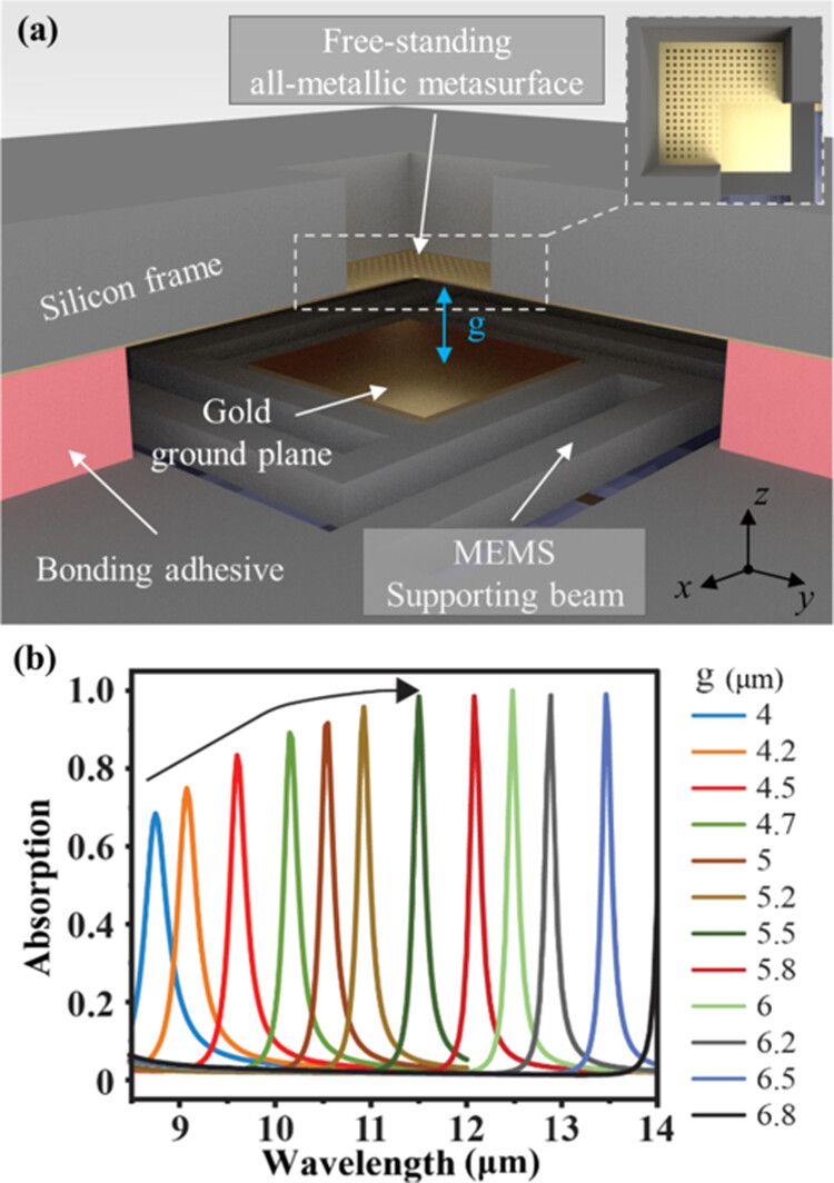
Figure 1. Schematic of the tunable metasurface absorber. (a) Cross-sectional view of the tunable absorber. The free-standing all-metallic metasurface is supported by a silicon frame. The gold ground plane is on a movable MEMS structure. The initial air gap between the metasurface and the ground plane is determined by the thickness of the bonding adhesive layer. We may tune the air gap through vertical actuation of the MEMS structure. (b) Simulated absorption spectra for different air gap thicknesses (g) under normal incidence, indicating that the absorption peak red-shifts as g increases.
To investigate the mechanism of the tunable absorption response, we employed an interference model to describe the coupling between metasurfaces and the FP cavity. The overall reflection (r) is the interference superposition of multiple reflected light in the cavity and it can be easily calculated using the following equation (38)
To investigate the mechanism of the tunable absorption response, we employed an interference model to describe the coupling between metasurfaces and the FP cavity. The overall reflection (r) is the interference superposition of multiple reflected light in the cavity and it can be easily calculated using the following equation (38)
In order to improve the conventional interference theory, we use the transmission line model to calculate the reflection and transmission coefficients by considering interlayer coupling between the metasurface and the ground plane. The equivalent circuit model of the absorber can be modeled as a parallel connection of the overall impedance of the metasurface (Zm) and the wave impedance of vacuum (Z0). Through impedance mismatch, Zm can be analytically derived from simulation results. And the effective reflection and transmission coefficients of metasurfaces can be subsequently retrieved from the transmission line model
Substituting the calculated coefficients into the interference model, we can match the corrected theoretical results of reflection and absorption with the full wave simulation. Figures 2a and S4 demonstrate the analytical and simulated absorption results of the absorber with a high degree of agreement, proving that by combining the transmission line model and interference theory, the behavior of the absorber can be appropriately described.
Figure 2

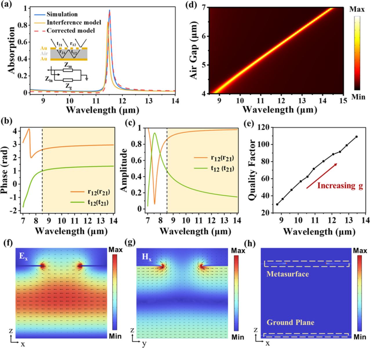
Figure 2. (a) Simulated and calculated results of the air-spaced absorber with an air gap g = 5.5 μm. The insets show the schematic of interference theory and the equivalent transmission line model. (b) Phase of calculated reflection and transmission coefficients of the metasurface from simulations for the metasurface unit cell. (c) Amplitude of the calculated reflection and transmission coefficients of the metasurface from simulations for the metasurface unit cell. (d) Absorption spectrum as a function of the air spacer thickness. (e) Simulated quality factor Q at different center absorption wavelengths. (f) Simulated electric field distribution in the cross-section (x–z plane). (g) Simulated magnetic field distribution in the cross-section (y–z plane). (h) Simulated power dissipation distribution in the cross-section (x–z plane).
We analyzed the electromagnetic properties of the individual free-standing metasurface layer to elucidate the underlying mechanism of the widely tunable response. The transmission and reflection coefficients exhibit smooth changes in phase and amplitude and the amplitude of reflection coefficients is close to 1 in wavelength ranges of interest, as shown in Figure 2b,c. It operates like a highly reflective phase retarder. According to interference theory, perfect absorption is induced by destructive interference of the reflected waves from the metasurface and the ground plane. In the perfect absorption state, the accumulated propagation phase from multiple reflections should satisfy the condition φ = 2mπ (m = 1, 2, ···). The total phase variation is mainly attributed from the phase delay caused by air gaps between metasurfaces and the gold ground plane. Therefore, we can tailor the absorption by manipulating the phase delay caused by air gaps while keeping the disruptive phase variations at the metasurface and the ground plane the same (Figure S5). However, the interlayer coupling between the metasurface and the ground plane will visually change the reflection and transmission properties of metasurfaces, thus causing a shift in the resonance wavelength. From the perspective of an equivalent circuit, the influence of interlayer coupling functions as an additional capacitance and an extra inductance resonator except for the inherent resonator capacitance and inductance of the metasurface. The great variation in fitted inductance manifests the influence of the interlayer coupling (Table S1). Figure 1d presents a simulated color map showing the evolution trends of the absorption spectrum with different air spacer thicknesses. We can see that a large tunable range from 8.5 to 14 μm can be realized by adjusting the air gap from 4 to 7 μm for first-order resonance. Actually, the high-order resonance mode at a larger air gap distance can also be used to manipulate absorptions as shown in Figure S6, which provides more flexibility in design.
The absorber demonstrates a high quality factor, as shown in Figure 2e, which originates from the strong coupled resonance mode between the complementary metasurface and the air-spaced Fabry–Perot cavity and the high reflection of the metasurface. Figure 2f,g illustrates the simulated electric field distribution and magnetic field distribution at the resonance wavelength. The electric field concentrates at the edges of the metallic hole and parallels in the cavity, indicating a coupling of the FP resonance and dipolar resonance. Moreover, due to the absence of the dielectric material in the spacer, the induced current entirely distributes in the metal meta-atom and ground plane, resulting in ohmic loss. As shown in Figure 2h, the power dissipation primarily occurs at the metasurface and ground plane with no losses in the spacer. The elimination of the dielectric materials in the absorber also contributes to the high quality factor (Figure S7). Despite the presence of ohmic loss in metal structures, the simulated quality factor increases to over 80 when g is ∼5.5 μm, over 2-fold higher than traditional dielectric-spaced devices. (20,36) Further improvement of the quality factor can be achieved by replacing Au with low-loss metals. In addition, according to interference theory, high-order absorption peaks exhibit much higher quality factors, but the undesired multistage resonance will greatly worsen the spectrum resolution.
The angular dispersion is an important merit in characterizing a metasurface absorber. To investigate the dispersive property of our absorber, we numerically construct the band diagrams for the TM- and TE-polarized excitations at different incident angles, proving its polarization- and angle- dependent narrowband absorptions. It should be noted that under normal incidence, both TE and TM responses for our absorber are identical, indicating a polarization-independent property due to its symmetrical design. However, under oblique incidence, polarization-dependent angular dispersion will be observed. Figure 3a,b shows the polarization-dependent angular dispersion for the absorber with a gap = 5.5 μm. We can see that the TE mode response displays a stable FP resonance mode of up to 30° with a maximum wavelength deviation of 1.5 μm. However, an extra surface plasmon resonance (SPR) mode of the metasurface is excited at an oblique angle of 10.5° for TM incidence and strongly couples with the FP resonance mode at 25°, causing an opposite trend of dispersion at large incidence. The FP and SPR modes have strong coupling effects on each other when the center resonance wavelength merges. Besides, the angular dispersion is also relevant to the air gap distance, as shown in Figures S8 and S9. When the air gap increases from 4.5 to 6.5 μm, larger dispersions and multiple resonance modes were emerged. The polarization dependence at the oblique incidence mainly arises from the polarization property of metasurfaces. However, the angular dispersion of the absorber may be attributed to the inherent angular dependence of both free-standing metasurface and the FP cavity, the former of which can be reduced and optimized by the angular-independent design of meta-atoms to realize a wide-angle absorption.
Figure 3

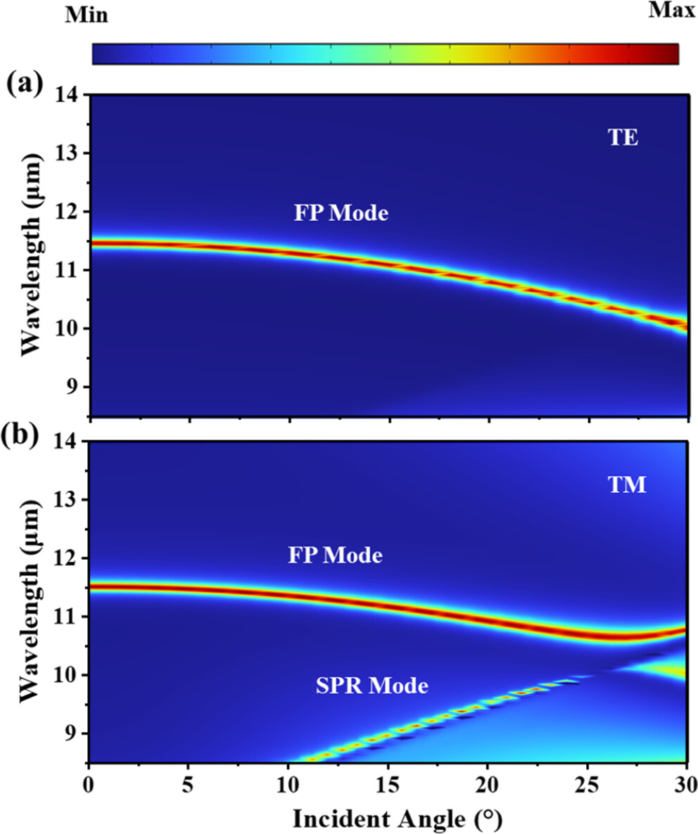
Figure 3. Simulated angular dispersion of the absorption for (a) TE and (b) TM incidence modes at g = 5.5 μm.
After judiciously designing the metasurface absorber, we developed a micromachining process to fabricate the proposed structure. One of the challenges in the fabrication is the patterning of the free-standing all-metal metasurface film. In most cases, metal metasurfaces of 100 nm or thinner thickness are fabricated on an additional, thin dielectric substrate like Si and silicon nitride. (17,18,20) The substrate layers will create spectral contaminants in the absorption and broaden the resonance peak due to the unwanted metal–substrate resonance and increased loss in the dielectric layer. In fact, the low strength of metals poses a long-standing challenge for fabricating a free-standing metasurface without substrates. To solve this problem, a wafer-scale micromachining method was developed. Figure 4a illustrates the fabrication process of the proposed metasurface absorber. First, photolithography was performed on a double-sided polished silicon wafer with high resistivity, and the metasurface arrays of 20 nm Cr/100 nm Au were patterned using e-beam evaporation and a lift-off process. Then, the metasurface was coated with a photoresist (PR) as the protective layer for the following steps. At the back side, a second photolithography with back side alignment was conducted to define the position and outline of the metasurface areas. Afterward, silicon below the metal patterns was completely removed by a deep reactive ion etching process, achieving the free-standing structures. And the wafer was carefully cleaned by acetone and treated with oxygen plasma for PR removal and cleaning. Large-scale metasurfaces ranging from 500 μm to 5 mm were fabricated and are shown in Figure 4b,c, demonstrating the good scalability of our microfabrication method. Besides, for optical applications, the flatness of the metasurface is crucial to obtain the desired spectral response as the local irregularity can cause an inhomogeneous response of meta-atoms. The surface morphology of the free-standing metasurface is characterized in Figure S11, showing a good flatness. The maximum roughness was less than 50 nm at the central region, while a height step of about 150 nm was localized at the transitions from the free-standing area to silicon substrates. It is probably due to the ion impact during the etching process, flattening the membrane and causing plastic deformation at the edges.
Figure 4

Figure 4. (a) Fabrication process flow of the metasurface and the absorber. (b) Photograph of the free-standing metasurface of 500 μm × 500 μm. (c) Photograph of the free-standing metasurface of diameter = 5 mm. (d) SEM image of the metasurface. The inset shows the thickness of the Cr/Au membrane. (e) Photograph of the fabricated absorber. (f) SEM cross-sectional image of the air gap spacer.
The SEM images of the metasurface are displayed in Figure 4d. A typical metasurface with a size of 500 × 500 μm includes about 71 × 71 unit array. It should be noted that the Cr adhesive layer exhibits negligible impacts on the optical property of the Au metasurface and can be further eliminated by ion beam etching if necessary (Figures S12 and S13). Next, we patterned the SU-8 frame structure on the other wafer to form a support to control the air space between the metasurface and the ground plane (Figure S16). In the final step, the wafer was flip-chip-bonded on the Au ground plane to form the absorber. Figure 4e shows the image of an integrated absorber of 5 mm × 5 mm with a metasurface size of 500 μm. The air gap was measured to be approximately 5.3 μm, as shown in Figure 4f, and the distance can be controlled by the thickness of SU-8.
To verify the tunable absorption response of our proposed absorber, a series of metadevices with varied SU-8 thicknesses of 4.1, 4.9, 5.1, 5.7, 6.4, and 6.7 μm were fabricated and characterized. We measured the reflection spectra in the wavelength ranging from 8.5 to 14 μm using the Fourier transform infrared spectroscopy (Bruker FTIR VERTEX 80v) in combination with IR microscopy (Hyperion 2000). The corresponding absorption was subsequently calculated, as shown in Figure 5. Actually, the actual distance may deviate from the designed SU-8 thickness after the bonding process. Considering the nonideal air spacer thickness, simulation results with the same peak absorption wavelength were employed to fit the measured results. We can see that with the increased air gap, the absorption peak gradually shifts to a long-wavelength region, which is in very good agreement with trends of the simulation results. The peak wavelength occurs at about twice the air gap thickness. The maximum absorption reaches 78% at 8.9 μm with an air gap = 4.1 μm. The result agrees well with the simulated value, but the peak absorption is smaller at other larger air gaps. It should be noted that some devices show relatively high background absorption and small fluctuations outside the resonance wavelength. The discrepancies between simulations and experiments can partially be attributed to unexpected multiple interference in the FP cavity caused by stray lights as well as systematic ripples in the FTIR characterization system during measurement. Another possible reason is that normal incidence is employed as the boundary condition for all simulations, while in the experiment, the incident waves are at different angles in the microscope configurations. The angular dispersion of absorbers discussed previously gives rise to a broadened spectrum and reduced peak values. The quality factors for all absorbers are measured to be 34.0, 45.7, 47.8, 49.4, 59.8, and 62.2, respectively. The quality factors improved by low dielectric losses are also smaller than simulations but still much higher than other previously reported metasurface devices, as illustrated in Table S2. In spite of these affecting factors, our design still shows a wide tunable range with a high quality factor for all air gaps.
Figure 5

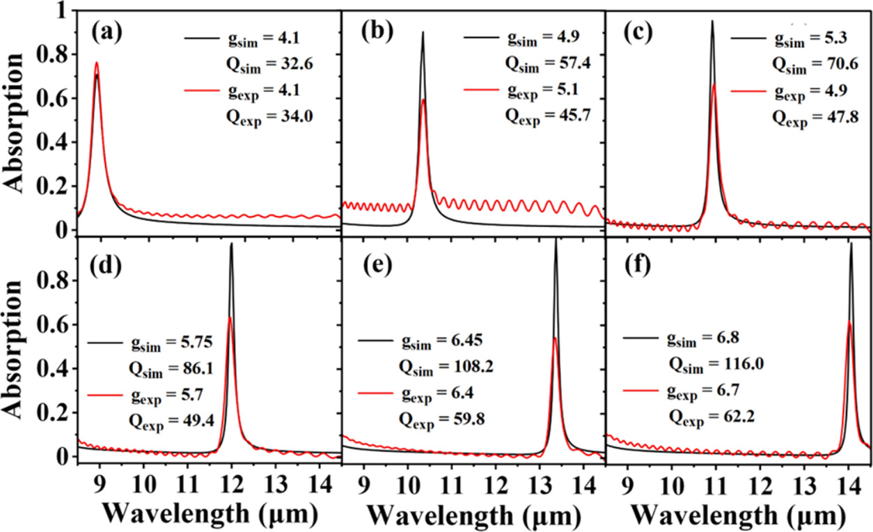
Figure 5. (a–f) Measured absorption spectra at different air gaps in comparison to simulation results.
MEMS electrostatic actuators have been widely used in building microelectro-opto-mechanical systems (40,41) due to their advantages in reconfigurability, fabrication compatibility, and further miniaturization. To realize the continuous adjustment of the air gap, we integrated the metasurface with a MEMS electrostatic actuator to construct a miniaturized infrared manipulation system, as shown in Figure 6a. The overall device consists of the metasurface chip, adhesive layer, electrostatic actuator, bottom electrode, and quartz substrate. Figure 6b illustrates the working principle of the proposed MEMS multifunctional infrared device. The device not only can work as an infrared switch but also have the ability to wide-range tunability. The actuator carrying the gold ground plane can move in the Z direction driven by electrostatic force. The air gap distance will change with the movement of the actuator, consequently resulting in a continuous tuning of absorptions. In the initial off-state, the absorber has a small air gap distance, achieving low absorption properties at the target long-wavelength infrared range. In the on-state, the driving voltage is applied to the bottom electrode. The actuator will be pulled downward, and the air gap distance will gradually increase with the increased voltage. As a result, the absorption spectra will be tuned to the long-infrared regime. The tunable range mainly depends on the strokes of the actuator, which is limited to the pull-in voltage. Figure 6c shows the fabricated MEMS actuator. The actuator is also fabricated by a standard micromachining process and can be easily integrated with the metasurface chip using a flip-chip bonding method. Figure 6d shows the fabricated MEMS tunable device. The size of the absorber chip is less than 1 cm × 1 cm.
Figure 6

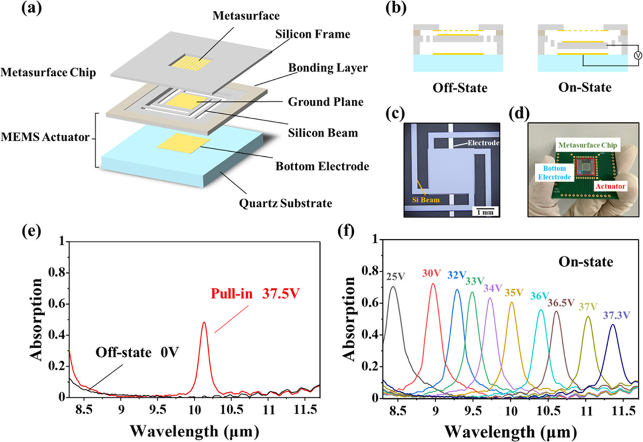
Figure 6. (a) Schematic of the MEMS tunable metasurface absorber. (b) The initial (off) state and actuated (on) state of the MEMS structure. (c) Photograph of the fabricated MEMS actuator. (d) Photograph of the fabricated MEMS tunable metasurface absorber. (e) Spectrum responses in the off-state and pull-in state. (f) Tunable absorption responses under different voltages in the on-state.
The infrared metadevice exhibits multiple functionalities for the dynamic manipulation of infrared radiations. Figure 6e,f shows the measured dynamic responses of the MEMS tunable absorber. We can see that in the off-state, the absorptivity at 8.5 to 14 μm is near zero. The device functions as a highly reflective mirror. In the on-state, when applying voltages from 25 to 37.3 V, the absorption peaks can be tuned from 8.4 to 11.4 μm continuously. The electrostatically actuated device shows low power consumption and has a modulation depth of up to 97%. The pull-in voltage is about 37.5 V, at which the actuator will be highly unstable and quickly snap down to the bottom electrode. In this circumstance, the air gap distance will be very large and high-order resonance can be observed. We demonstrated the switchable and tunable ability of the proposed MEMS actuator–metasurface configuration. The dynamic range of the fabricated device is about 3 μm, which is smaller than our design but is still much larger than those of previous MEMS-based tunable devices. It is mainly limited to the maximum actuation displacement of the electrostatic actuator, which is approximately 3 μm (Figure S21). By the design of large-stroke actuators, a tuning range from 8.5 to 14 μm can be realized in the future. It has also been observed that the absorption decreases as the tuning voltage increases. In addition to the influence of angular dispersions discussed previously, the fabrication defects may also have an impact on the absorption performance in the multifunctional devices. The reflection of the gold ground plane may be decreased due to the surface roughness of the silicon plate compared to the gold mirror with total reflection, thus causing the decreased absorption of the absorbers. This issue can be addressed by adding a polishing process in fabrications.
In summary, we present a scheme to implement a tunable narrowband long-infrared absorber with high quality factors and an excellent spectral resolution by combining a free-standing metasurface and an air-spaced FP cavity. High absorption from 8.5 to 14 μm can be realized by changing the air gap between the metasurface and the ground plane from 4 to 7 μm. Due to the absence of the dielectric spacer, the quality factor is greatly increased. A wafer-scaled microfabrication method is developed to fabricate a free-standing, 100-nm-thick metasurface. Absorbers with different air gaps were built and demonstrated, proving a good absorption spectrum and a wide tunable range of our design. MEMS-based tunable metasurface devices are proposed and fabricated, realizing the miniaturized dynamic manipulation system. The demonstrated MEMS–metasurface architecture can be further expanded by integrating different metasurfaces and large-stroke actuators to realize a full tunable range covering both middle- and long-wavelength infrared ranges. We believe that this work presents a practical and effective solution for realizing dynamic infrared light manipulation with full flexibility and high performance. In the future, we aim to integrate a microhot plate with the MEMS tunable absorber to achieve a tunable infrared emitter which is competent for gas sensing, thermal camouflage, and other potential applications.


